KR102732599B1 - Method for selectively transferring micro LEDs - Google Patents
Method for selectively transferring micro LEDs Download PDFInfo
- Publication number
- KR102732599B1 KR102732599B1 KR1020220089024A KR20220089024A KR102732599B1 KR 102732599 B1 KR102732599 B1 KR 102732599B1 KR 1020220089024 A KR1020220089024 A KR 1020220089024A KR 20220089024 A KR20220089024 A KR 20220089024A KR 102732599 B1 KR102732599 B1 KR 102732599B1
- Authority
- KR
- South Korea
- Prior art keywords
- substrate
- micro led
- led chips
- sheet
- panel
- Prior art date
- Legal status (The legal status is an assumption and is not a legal conclusion. Google has not performed a legal analysis and makes no representation as to the accuracy of the status listed.)
- Active
Links
Images


Classifications
-
- H—ELECTRICITY
- H10—SEMICONDUCTOR DEVICES; ELECTRIC SOLID-STATE DEVICES NOT OTHERWISE PROVIDED FOR
- H10W—GENERIC PACKAGES, INTERCONNECTIONS, CONNECTORS OR OTHER CONSTRUCTIONAL DETAILS OF DEVICES COVERED BY CLASS H10
- H10W72/00—Interconnections or connectors in packages
- H10W72/01—Manufacture or treatment
- H10W72/0198—Manufacture or treatment batch processes
-
- H01L24/95—
-
- H01L33/0093—
-
- H—ELECTRICITY
- H10—SEMICONDUCTOR DEVICES; ELECTRIC SOLID-STATE DEVICES NOT OTHERWISE PROVIDED FOR
- H10H—INORGANIC LIGHT-EMITTING SEMICONDUCTOR DEVICES HAVING POTENTIAL BARRIERS
- H10H20/00—Individual inorganic light-emitting semiconductor devices having potential barriers, e.g. light-emitting diodes [LED]
- H10H20/01—Manufacture or treatment
- H10H20/011—Manufacture or treatment of bodies, e.g. forming semiconductor layers
- H10H20/018—Bonding of wafers
-
- H01L2224/95053—
Landscapes
- Led Device Packages (AREA)
- Led Devices (AREA)
- Electroluminescent Light Sources (AREA)
Abstract
본 발명의 마이크로 LED 칩 선택적 전사 방법은 폴리디메틸실록산(PDMS) 시트를 제1 기판 상에 부착하는 공정; 마이크로 LED 칩들이 배열된 웨이퍼를 상기 마이크로 LED 칩들이 상기 PDMS 시트에 대향하도록 상기 PDMS 시트 상에 정렬한 후 상기 웨이퍼와 상기 제1 기판을 압착하는 공정; 레이저 리프트 오프 공정을 통해 상기 마이크로 LED 칩들을 상기 제1 기판 상에 전사하는 공정; 제2 기판상에 온도, 압력, 가스분위기, 빛의 파장 중 적어도 하나 이상의 환경조건에 따라 접착력이 발생 또는 소멸 또는 약화되는 환경 가변 점착 시트를 부착하는 공정; 상기 마이크로 LED 칩들이 배열된 상기 제1 기판을 상기 마이크로 LED 칩들이 상기 환경 가변 점착 시트에 대향하도록 상기 환경 가변 점착 시트 상에 정렬한 후 고온 가압 전사 공정을 통해 상기 제1 기판의 상기 마이크로 LED 칩들을 상기 제2 기판 상에 전사하는 공정; 상기 제2 기판을 적어도 하나의 선택적 위치에 본딩 패드가 형성된 패널에 정렬하고 상기 제2 기판을 상기 패널에 접합하는 공정; 상기 선택적 위치에 레이저를 조사하는 공정; 및 상기 제2 기판을 상기 패널로부터 분리하는 공정;을 포함할 수 있다.The method for selectively transferring micro LED chips of the present invention comprises: a process of attaching a polydimethylsiloxane (PDMS) sheet onto a first substrate; a process of aligning a wafer on which micro LED chips are arranged on the PDMS sheet so that the micro LED chips face the PDMS sheet, and then pressing the wafer and the first substrate; a process of transferring the micro LED chips onto the first substrate through a laser lift-off process; a process of attaching an environmentally variable adhesive sheet, the adhesive strength of which is generated, extinguished, or weakened depending on at least one environmental condition of temperature, pressure, gas atmosphere, and light wavelength, onto a second substrate; a process of aligning the first substrate on which the micro LED chips are arranged so that the micro LED chips face the environmentally variable adhesive sheet, and then transferring the micro LED chips of the first substrate onto the second substrate through a high-temperature and pressurization transfer process; a process of aligning the second substrate to a panel on which bonding pads are formed at at least one selective location, and bonding the second substrate to the panel; a process of irradiating a laser at the selective location; and a process of separating the second substrate from the panel;
Description
본 발명은 마이크로 LED 선택적 전사 방법에 관한 것이다. The present invention relates to a micro LED selective transfer method.
LED 칩을 이용한 고화질 디스플레이의 개발이 활발히 진행되고 있다. 구동 회로가 구비된 백플레인 기판의 단위 픽셀 전극 라인 위에 LED 칩을 직접 실장하게 된다.The development of high-definition displays using LED chips is actively underway. LED chips are mounted directly on the unit pixel electrode lines of a backplane substrate equipped with a driving circuit.
최근에는 고화소 디스플레이를 위한 단위 픽셀 크기가 감소됨에 따라서 크기가 100 ㎛ 이하로 매우 작은 마이크로 LED 칩이 사용되고 있다. 이로 인해 일반적인 픽 앤 플레이스 기구(pick and place machine)를 이용하여 백플레인 기판 위에 마이크로 LED 칩을 직접 실장하는 공정을 선택하는 경우, 공정 시간이 크게 늘어나고, 실장 오류 발생률이 높아질 수 있다.Recently, as the unit pixel size for high-resolution displays decreases, very small micro LED chips of 100 ㎛ or less in size are being used. Therefore, if a process of directly mounting micro LED chips on a backplane substrate using a general pick and place machine is selected, the process time may significantly increase and the mounting error rate may increase.
이러한 문제점을 해소하기 위해서, 다수의 마이크로 LED 칩을 백플레인 기판에 한꺼번에 실장하는 마이크로 LED 칩의 대량 전사기술이 다양하게 개발되고 있다.To solve these problems, various mass transfer technologies for micro LED chips are being developed to simultaneously mount a large number of micro LED chips on a backplane substrate.
이러한 대량 전사 기술에는 정전기력을 이용한 방법, 자기력을 이용한 방법, 점착력을 이용한 방법이 있다.These mass transfer techniques include methods that utilize electrostatic force, methods that utilize magnetic force, and methods that utilize adhesive force.
이러한 다수의 마이크로 LED 칩을 기판에 한꺼번에 실장하는 마이크로 LED 칩의 대량 전사기술은 개발되고 있지만, 캐리어 기판에 실장된 다수의 마이크로 LED 칩들 중 일부만을 기판에 전사하는 기술이 요구되고 있다. A mass transfer technology for mounting a large number of micro LED chips on a substrate at once is being developed, but a technology for transferring only some of the large number of micro LED chips mounted on a carrier substrate to the substrate is required.
즉, 10마이크로미터 이하의 극소형 픽셀 크기의 마이크로 LED들 중 일부만을 원하는 기판으로 전사하는 기술이 당업계에 요구되고 있다. That is, a technology for transferring only a portion of micro LEDs with an ultra-small pixel size of 10 micrometers or less to a desired substrate is required in the art.
본 발명은 다수의 마이크로 LED들 중 일부를 기판 상에 전사할 수 있는 마이크로 LED 선택적 전사 방법을 제공하는 데 그 목적이 있다.The purpose of the present invention is to provide a micro LED selective transfer method capable of transferring some of a plurality of micro LEDs onto a substrate.
상기와 같은 목적을 달성하기 위한 본 발명에 따른 마이크로 LED 칩 선택적 전사 방법은 폴리디메틸실록산(PDMS) 시트를 제1 기판 상에 부착하는 제1 공정; 마이크로 LED 칩들이 배열된 웨이퍼를 상기 마이크로 LED 칩들이 상기 PDMS 시트에 대향하도록 상기 PDMS 시트 상에 정렬한 후 상기 웨이퍼와 상기 제1 기판을 압착하는 제2 공정; 레이저 리프트 오프 공정을 통해 상기 마이크로 LED 칩들을 상기 제1 기판 상에 전사하는 제3 공정; 제2 기판상에 환경 가변 점착 시트를 부착하는 제4 공정; 상기 마이크로 LED 칩들이 배열된 상기 제1 기판을 상기 마이크로 LED 칩들이 상기 환경 가변 점착 시트에 대향하도록 상기 제2 기판 상에 정렬한 후 고온 가압 전사 공정을 통해 상기 제1 기판의 상기 마이크로 LED 칩들을 상기 제2 기판 상에 전사하는 제5 공정; 상기 제2 기판을 적어도 하나의 선택적 위치에 본딩 패드가 형성된 패널에 정렬하고 상기 제2 기판을 상기 패널에 접합하는 제6 공정; 상기 선택적 위치에 레이저를 조사하는 제7 공정; 및 상기 제2 기판을 상기 패널로부터 분리하는 제8 공정;을 포함한다.In order to achieve the above object, the present invention provides a method for selectively transferring micro LED chips, comprising: a first process of attaching a polydimethylsiloxane (PDMS) sheet onto a first substrate; a second process of aligning a wafer on which micro LED chips are arranged on the PDMS sheet so that the micro LED chips face the PDMS sheet, and then pressing the wafer and the first substrate; a third process of transferring the micro LED chips onto the first substrate through a laser lift-off process; a fourth process of attaching an environmentally variable adhesive sheet onto a second substrate; a fifth process of aligning the first substrate on which the micro LED chips are arranged on the second substrate so that the micro LED chips face the environmentally variable adhesive sheet, and then transferring the micro LED chips of the first substrate onto the second substrate through a high-temperature and pressurization transfer process; a sixth process of aligning the second substrate to a panel on which bonding pads are formed at at least one selective location, and bonding the second substrate to the panel; a seventh process of irradiating a laser at the selective location; and an eighth process of separating the second substrate from the panel.
상기 환경 가변 점착 시트는 온도, 압력, 가스분위기, 빛의 파장 중 적어도 하나 이상의 환경조건에 따라 접착력이 발생 또는 소멸 또는 약화될 수 있다. The above environmentally variable adhesive sheet can have adhesive strength generated, extinguished, or weakened depending on at least one environmental condition of temperature, pressure, gas atmosphere, and light wavelength.
상기 환경 가변 점착 시트는 특정 온도범위 내에서는 접착력이 발생하고, 특정 온도범위를 벗어나면 접착력이 소멸 또는 0.1N 이하로 약화되는 열변화시트 또는 열변화테이프를 포함할 수 있다. The above environmentally variable adhesive sheet may include a heat-change sheet or heat-change tape in which adhesive strength is generated within a specific temperature range and the adhesive strength disappears or weakens to 0.1 N or less when the specific temperature range is exceeded.
상기 환경 가변 점착 시트는 빛의 특정한 파장 범위에서 접착력이 발생하고, 특정 파장 범위를 벗어나면 접착력이 소멸 또는 약화될 수 있다. The above environmentally variable adhesive sheet has adhesive strength that occurs within a specific wavelength range of light, and the adhesive strength may disappear or weaken when the wavelength range is exceeded.
상기 본딩 패드중 일부는 상기 제2 기판과 상기 패널을 정렬시킬 때 기준점이 되는 기준 마크로서 기능할 수 있다.Some of the above bonding pads may function as reference marks that serve as reference points when aligning the second substrate and the panel.
상기 제1 기판 및 상기 제2 기판은 유리 기판일 수 있다.The first substrate and the second substrate may be glass substrates.
상기 제7 공정은 LIFT(Laser-Induced-Forward-Transfer) 방식을 이용할 수 있다.The above seventh process can utilize the LIFT (Laser-Induced-Forward-Transfer) method.
상기 제1 공정 및 상기 제2 공정은 상온 환경에서 수행될 수 있다. The above first process and the above second process can be performed in a room temperature environment.
본 발명에 따른 마이크로 LED 선택적 전사 방법에 따르면, 웨이퍼에서 형성된 복수개의 LED 칩들 중 선택된 마이크로 LED 칩들을 용이하게 원하는 기판으로 전사할 수 있다.According to the micro LED selective transfer method according to the present invention, selected micro LED chips among a plurality of LED chips formed on a wafer can be easily transferred to a desired substrate.
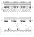
도 1은 본 발명의 실시예에 따른 마이크로 LED 선택적 전사 방법의 제1 공정을 설명하기 위한 도면.
도 2는 본 발명의 실시예에 따른 마이크로 LED 선택적 전사 방법의 제2 공정을 설명하기 위한 도면.
도 3은 본 발명의 실시예에 따른 마이크로 LED 선택적 전사 방법의 제3 공정을 설명하기 위한 도면.
도 4은 본 발명의 실시예에 따른 마이크로 LED 선택적 전사 방법의 제4 공정을 설명하기 위한 도면.
도 5는 본 발명의 실시예에 따른 마이크로 LED 선택적 전사 방법의 제5 공정을 설명하기 위한 도면.
도 6은 본 발명의 실시예에 따른 마이크로 LED 선택적 전사 방법의 제6 공정을 설명하기 위한 도면.
도 7은 본 발명의 실시예에 따른 마이크로 LED 선택적 전사 방법의 제7 공정 을 제8 공정을 설명하기 위한 도면.FIG. 1 is a drawing for explaining a first process of a micro LED selective transfer method according to an embodiment of the present invention.
FIG. 2 is a drawing for explaining a second process of a micro LED selective transfer method according to an embodiment of the present invention.
FIG. 3 is a drawing for explaining a third process of a micro LED selective transfer method according to an embodiment of the present invention.
FIG. 4 is a drawing for explaining a fourth process of a micro LED selective transfer method according to an embodiment of the present invention.
FIG. 5 is a drawing for explaining a fifth process of a micro LED selective transfer method according to an embodiment of the present invention.
FIG. 6 is a drawing for explaining a sixth process of a micro LED selective transfer method according to an embodiment of the present invention.
FIG. 7 is a drawing for explaining the seventh process and the eighth process of the micro LED selective transfer method according to an embodiment of the present invention.
이하의 내용은 단지 본 발명의 원리를 예시한다. 그러므로 당업자는 비록 본 명세서에 명확히 설명되거나 도시되지 않았지만, 본 발명의 원리를 구현하고 본 발명의 개념과 범위에 포함된 다양한 장치를 발명할 수 있는 것이다.The following merely illustrates the principles of the present invention. Therefore, those skilled in the art will be able to invent various devices that implement the principles of the present invention and are included within the concept and scope of the present invention, even though they are not explicitly described or illustrated in the specification.
또한, 본 명세서에 열거된 모든 조건부 용어 및 실시 예들은 원칙적으로, 본 발명의 개념이 이해되도록 하기 위한 목적으로만 명백히 의도되고, 이와 같이 특별히 열거된 실시 예들 및 상태들에 제한적이지 않는 것으로 이해되어야 한다.Furthermore, it should be understood that all conditional terms and embodiments listed in this specification are, in principle, expressly intended only for the purpose of making the concept of the present invention understood, and are not limited to the embodiments and conditions specifically listed as such.
본 발명을 설명함에 있어서 제1, 제2 등의 용어는 다양한 구성요소들을 설명하는데 사용될 수 있지만, 구성요소들은 용어들에 의해 한정되지 않을 수 있다.In describing the present invention, terms such as first, second, etc. may be used to describe various components, but the components may not be limited by the terms.
예를 들어, 본 발명의 권리 범위를 벗어나지 않으면서 제1 구성요소는 제2 구성요소로 명명될 수 있고, 유사하게 제2 구성요소도 제1 구성요소로 명명될 수 있다.For example, without departing from the scope of the present invention, the first component could be named the second component, and similarly, the second component could also be named the first component.
어떤 구성요소가 다른 구성요소에 연결되어 있다거나 접속되어 있다고 언급되는 경우는, 그 다른 구성요소에 직접적으로 연결되어 있거나 또는 접속되어 있을 수도 있지만, 중간에 다른 구성요소가 존재할 수도 있다고 이해될 수 있다.When it is said that a component is connected or coupled to another component, it can be understood that it may be directly connected or coupled to that other component, but there may also be other components in between.
본 명세서에서 사용한 용어는 단지 특정한 실시예를 설명하기 위해 사용된 것으로, 본 발명을 한정하려는 의도가 아니며, 단수의 표현은 문맥상 명백하게 다르게 뜻하지 않는 한, 복수의 표현을 포함할 수 있다.The terminology used herein is for the purpose of describing particular embodiments only and is not intended to limit the present invention, and the singular expression may include the plural expression unless the context clearly indicates otherwise.
본 명세서에서, 포함하다 또는 구비하다 등의 용어는 명세서상에 기재된 특징, 숫자, 공정, 동작, 구성요소, 부품 또는 이들을 조합한 것이 존재함을 지정하려는 것으로서, 하나 또는 그 이상의 다른 특징들이나 숫자, 공정, 동작, 구성요소, 부품 또는 이들을 조합한 것들의 존재 또는 부가 가능성을 미리 배제하지 않는 것으로 이해될 수 있다.In this specification, terms such as “include” or “have” are intended to specify the presence of a feature, number, process, operation, component, part or combination thereof described in the specification, and can be understood as not excluding in advance the possibility of the presence or addition of one or more other features, numbers, processes, operations, components, parts or combinations thereof.
본 발명의 일 실시예에 따른 마이크로 LED 선택적 전사 방법은 폴리디메틸실록산(PDMS) 시트를 제1 기판 상에 부착하는 제1 공정, 마이크로 LED 칩들이 배열된 웨이퍼를 상기 마이크로 LED 칩들이 상기 PDMS 시트에 대향하도록 상기 PDMS 시트 상에 정렬한 후 상기 웨이퍼와 상기 제1 기판을 압착하는 제2 공정, 레이저 리프트 오프 공정을 통해 상기 마이크로 LED 칩들을 상기 제1 기판 상에 전사하는 제3 공정, 제2 기판상에 환경 가변 점착 시트를 부착하는 제4 공정, 상기 마이크로 LED 칩들이 배열된 상기 제1 기판을 상기 마이크로 LED 칩들이 상기 환경 가변 점착 시트에 대향하도록 상기 제2 기판 상에 정렬한 후 고온 가압 전사 공정을 통해 상기 제1 기판의 상기 마이크로 LED 칩들을 상기 제2 기판 상에 전사하는 제5 공정, 상기 제2 기판을 적어도 하나의 선택적 위치에 본딩 패드가 형성된 패널에 정렬하고 상기 제2 기판을 상기 패널에 접합하는 제6 공정, 상기 선택적 위치에 레이저를 조사하는 제7 공정, 및 상기 제2 기판을 상기 패널로부터 분리하는 제8 공정을 포함한다. According to one embodiment of the present invention, a micro LED selective transfer method includes a first process of attaching a polydimethylsiloxane (PDMS) sheet onto a first substrate, a second process of aligning a wafer having micro LED chips arranged thereon on the PDMS sheet so that the micro LED chips face the PDMS sheet, and then pressing the wafer and the first substrate, a third process of transferring the micro LED chips onto the first substrate through a laser lift-off process, a fourth process of attaching an environmentally variable adhesive sheet onto a second substrate, a fifth process of aligning the first substrate having the micro LED chips arranged thereon on the second substrate so that the micro LED chips face the environmentally variable adhesive sheet, and then transferring the micro LED chips of the first substrate onto the second substrate through a high-temperature and pressurization transfer process, a sixth process of aligning the second substrate to a panel having bonding pads formed at at least one selective location and bonding the second substrate to the panel, a seventh process of irradiating a laser at the selective location, and an eighth process of separating the second substrate from the panel.
이하, 첨부된 도면을 참조하면서 본 발명의 바람직한 실시 예에 따른 마이크로 LED칩 분리 및 전사방법에 대하여 상세하게 설명한다. Hereinafter, a micro LED chip separation and transfer method according to a preferred embodiment of the present invention will be described in detail with reference to the attached drawings.
본 발명의 실시예에 따른 마이크로 LED 선택적 전사 방법은 폴리디메틸실록산(polydimethylsiloxane: PDMS) 시트(120)를 제1 기판(110a) 상에 부착하는 공정(제1 공정)를 포함한다. 상기 제1 공정은 상온 환경에서 수행될 수 있다. 상온 온도 범위는 영상 15도 내지 영상 25도의 범위를 말한다.A micro LED selective transfer method according to an embodiment of the present invention includes a process (first process) of attaching a polydimethylsiloxane (PDMS) sheet (120) onto a first substrate (110a). The first process can be performed in a room temperature environment. The room temperature range refers to a range of 15 degrees Celsius to 25 degrees Celsius.
제1 기판(110a)는 유리 기판일 수 있다.The first substrate (110a) may be a glass substrate.
폴리디메틸실록산(polydimethylsiloxane: PDMS) 시트는 제1 기판(110a)의 상대적으로 넓은 영역에 안정적으로 점착할 수 있는 합성고무 재질이며, 평탄하지 않은 표면에도 동일하게 안정적으로 점착 할 수 있다는 장점을 가지고 있다. 도 1을 참조하면, 캐리어 필름(20)이 일면에 부착된 PDMS 시트(120)를 제1 기판(110a)상에 라미네이션 후 캐리어 필름(20)을 제거한다. A polydimethylsiloxane (PDMS) sheet is a synthetic rubber material that can stably adhere to a relatively wide area of a first substrate (110a), and has the advantage of being able to stably adhere to an uneven surface. Referring to Fig. 1, a PDMS sheet (120) having a carrier film (20) attached to one surface is laminated onto a first substrate (110a), and then the carrier film (20) is removed.
구체적으로, 캐리어 필름(20)이 일면에 부착된 PDMS 시트(120)를 PDMS 시트(120)의 다른 면이 상기 제1 기판(110a)에 대향하도록 배치한 후 한 쌍의 롤 라미네이터들(10a, 10b) 사이에 위치시킨다. 이어서, 한 쌍의 롤 라미네이터들(10a, 10b)로 PDMS 시트(120)와 제1 기판(110a)를 가압하여 PDMS 시트(120)를 제1 기판(110a)에 부착시킨다. 이후, PDMS 시트(120)의 일면에 부착된 캐리어 필름(20)을 제거한다.Specifically, a PDMS sheet (120) having a carrier film (20) attached to one surface thereof is positioned so that the other surface of the PDMS sheet (120) faces the first substrate (110a), and then positioned between a pair of roll laminators (10a, 10b). Then, the PDMS sheet (120) and the first substrate (110a) are pressed by the pair of roll laminators (10a, 10b) to attach the PDMS sheet (120) to the first substrate (110a). Thereafter, the carrier film (20) attached to one surface of the PDMS sheet (120) is removed.
이어서, 본 발명의 실시예에 따른 마이크로 LED 선택적 전사 방법은 마이크로 LED 칩들(200)이 배열된 웨이퍼(30)를 상기 마이크로 LED 칩들(200)이 상기 PDMS 시트(120)에 대향하도록 상기 PDMS 시트(120) 상에 정렬한 후 상기 웨이퍼(30)와 상기 제1 기판(110a)을 압착하는 공정(제2 공정)를 포함한다. 상기 제2 공정은 상온 환경에서 수행될 수 있다. Next, the micro LED selective transfer method according to an embodiment of the present invention includes a process (second process) of aligning a wafer (30) having micro LED chips (200) arranged thereon on a PDMS sheet (120) so that the micro LED chips (200) face the PDMS sheet (120), and then pressing the wafer (30) and the first substrate (110a). The second process can be performed in a room temperature environment.
구체적으로, 도 2를 참조하면, 웨이퍼(30) 상에 복수개의 마이크로 LED 칩(Light emitting element chip)을 형성한다. 웨이퍼(30)는 사파이어 웨이퍼인 것이 바람직하다. 이어서, 웨이퍼(30) 상에 형성된 복수개의 마이크로 LED 칩들(200) 상에 접합층(bonding layer)(210)을 형성한다. 접합층(210)은 주석(Sn) 접합 소재(bonding material) 또는 인듐(In) 접합 소재를 포함할 수 있다. 상기 접합층은 마이크로 LED 본딩패드(bonding pad) 혹은 TFT 패널 본딩패드에 도금 공정을 통해 형성할 수 있다. Specifically, referring to FIG. 2, a plurality of micro LED chips (Light emitting element chips) are formed on a wafer (30). The wafer (30) is preferably a sapphire wafer. Next, a bonding layer (210) is formed on the plurality of micro LED chips (200) formed on the wafer (30). The bonding layer (210) may include a tin (Sn) bonding material or an indium (In) bonding material. The bonding layer may be formed on a micro LED bonding pad or a TFT panel bonding pad through a plating process.
마이크로 LED 칩들(200)이 배열된 웨이퍼(30)를 상기 마이크로 LED 칩들(200)이 상기 PDMS 시트(120)에 대향하도록 상기 PDMS 시트(120) 상에 정렬한 후 상기 웨이퍼(30)와 상기 제1 기판(110a)을 가압한다. 이 경우, 제1 기판(110a)의 하부에 하부 스테이지(40)를 위치시켜, 제1 기판(110a)을 지지할 수 있다.After aligning the wafer (30) on which the micro LED chips (200) are arranged on the PDMS sheet (120) so that the micro LED chips (200) face the PDMS sheet (120), the wafer (30) and the first substrate (110a) are pressed. In this case, the lower stage (40) may be positioned below the first substrate (110a) to support the first substrate (110a).
이어서, 본 발명의 실시예에 따른 마이크로 LED 선택적 전사 방법은 레이저 리프트 오프 공정을 통해 상기 마이크로 LED 칩들을 상기 제1 기판 상에 전사하는 공정(제3 공정)를 포함한다. Next, the micro LED selective transfer method according to an embodiment of the present invention includes a process (third process) of transferring the micro LED chips onto the first substrate through a laser lift-off process.
도 3을 참조하면, 상기 제2 공정 후에 웨이퍼(30)상의 마이크로 LED 칩들(200)이 제1 기판(110a) 상의 PDMS 시트(120)에 접촉하게 된다. Referring to FIG. 3, after the second process, the micro LED chips (200) on the wafer (30) come into contact with the PDMS sheet (120) on the first substrate (110a).
구체적으로, 레이저 리프트 오프(Laser lift off) 공정을 통해 웨이퍼(30) 상에 형성된 복수개의 마이크로 LED 칩들(200) 전체가 웨이퍼(30)로부터 분리되어 제1 기판(110a)의 PDMS 시트(120)에 부착된다. 레이저 리프트 오프(LLO) 공정은 복수개의 마이크로 LED 칩들(200)가 형성된 웨이퍼(30)를 레이저에 노출시킴으로써 복수개의 마이크로 LED 칩들(200)와 웨이퍼(30) 사이의 결합력을 제거하는 공정이다. Specifically, a plurality of micro LED chips (200) formed on a wafer (30) are separated from the wafer (30) through a laser lift off process and attached to a PDMS sheet (120) of a first substrate (110a). The laser lift off (LLO) process is a process of removing the bonding force between the plurality of micro LED chips (200) and the wafer (30) by exposing the wafer (30) on which the plurality of micro LED chips (200) are formed to a laser.
이러한 레이저 리프트 오프 공정을 통해 상기 마이크로 LED 칩들(200)이 상기 제1 기판(110a) 상에 전사될 수 있다. 마이크로 LED 칩들(200)이 웨이퍼(30)로부터 분리될 때, 마이크로 LED 칩들(200) 상에 형성된 접합층(210)으로 인해 마이크로 LED 칩들(200)이 PDMS 시트(120)에 용이하게 접착될 수 있다. Through this laser lift-off process, the micro LED chips (200) can be transferred onto the first substrate (110a). When the micro LED chips (200) are separated from the wafer (30), the micro LED chips (200) can be easily adhered to the PDMS sheet (120) due to the bonding layer (210) formed on the micro LED chips (200).
이어서, 본 발명의 실시예에 따른 마이크로 LED 선택적 전사 방법은 제2 기판(110b))상에 환경 가변 점착 시트(130)를 부착하는 공정(제4 공정)를 포함한다.Next, the micro LED selective transfer method according to the embodiment of the present invention includes a process (fourth process) of attaching an environmentally variable adhesive sheet (130) on a second substrate (110b).
제2 기판(110b)는 유리 기판일 수 있다.The second substrate (110b) may be a glass substrate.
환경 가변 점착 시트(130)는 온도, 압력, 가스분위기, 빛의 파장 중 적어도 하나 이상의 환경조건에 따라 점착력이 발생 또는 소멸 또는 약화될 수 있다. 즉, 환경 가변 점착 시트의 소재가 온도, 압력, 가스분위기, 빛의 파장 중 적어도 하나에 대해 반응할 수 있다. The environmentally variable adhesive sheet (130) can have adhesive strength generated, extinguished, or weakened depending on at least one environmental condition of temperature, pressure, gas atmosphere, and light wavelength. That is, the material of the environmentally variable adhesive sheet can react to at least one of temperature, pressure, gas atmosphere, and light wavelength.
예컨대, 제4공정에서 적용될 수 있는 환경 가변 점착 시트(130)는 특정 온도범위 내에서는 접착력이 발생하고 특정 온도범위를 벗어나면 접착력이 소멸 또는 약화되는 접착제가 도포된 열변화시트 또는 열변화테이프를 적용할 수도 있고, 이와 다르게, 특정한 파장 조건의 빛을 받으면 접착력이 발생하고 특정 파장 조건을 벗어나면 접착력이 소멸 또는 약화되는 특성을 가지는 소재를 적용할 수도 있으며, 특정 가스 분위기에서는 접착력이 발생하고, 특정 가스 분위기가 해제되면 접착력이 소멸 또는 약화되는 특성을 가지는 것을 적용할 수도 있다.For example, as an environmentally variable adhesive sheet (130) that can be applied in the fourth process, a heat-change sheet or heat-change tape coated with an adhesive that generates adhesive force within a specific temperature range and disappears or weakens when the temperature range is exceeded may be applied, or, differently, a material that has a characteristic of generating adhesive force when exposed to light of a specific wavelength condition and disappearing or weakening the adhesive force when the specific wavelength condition is exceeded may be applied, or a material that has a characteristic of generating adhesive force in a specific gas atmosphere and disappearing or weakening the adhesive force when the specific gas atmosphere is released may be applied.
상기 환경 가변 점착 시트(130)는 폴리머를 이용하여 시트 형태로 형성될 수 있으며, 이 폴리머 시트는 PET(Polyethylene terephthalate), PEN(Polyethylene naphthalate), PA(Polyamide), PI(Polyimide), PC(polycarbonate), PVC(Polyvinyl Chloride), 쿼츠(Quartz), 유리(Glass), 금속(Metal), 플라스틱(Plastic) 소재를 포함하여 형성된 지그 또는 탄성을 갖는 소재로 형성된 지지체에 형성될 수 있다. The above-mentioned environment variable adhesive sheet (130) can be formed in a sheet shape using a polymer, and the polymer sheet can be formed on a jig formed including PET (Polyethylene terephthalate), PEN (Polyethylene naphthalate), PA (Polyamide), PI (Polyimide), PC (polycarbonate), PVC (Polyvinyl Chloride), Quartz, Glass, Metal, Plastic, or a support formed of an elastic material.
한편, 상기 환경 가변 점착 시트(130)는 온도차이에 의해 접착력이 발생 또는 소멸 또는 약화되는 구조를 적용할 수도 있다. 이 경우, 환경 가변 점착 시트(130)는 80도(℃)의 온도에서 점착력이 높으나 3도 이하의 온도에서 점착력이 낮은 전사 소재로 이루어질 수 있다.Meanwhile, the environment variable adhesive sheet (130) may also apply a structure in which adhesive force is generated, extinguished, or weakened by a temperature difference. In this case, the environment variable adhesive sheet (130) may be made of a transfer material that has high adhesive force at a temperature of 80 degrees (℃) but low adhesive force at a temperature of 3 degrees or lower.
도 4를 참조하면, 캐리어 필름(22)이 일면에 부착된 환경 가변 점착 시트(130)를 제2 기판(110b)상에 라미네이션 후 캐리어 필름(22)을 제거한다. Referring to Fig. 4, an environmentally variable adhesive sheet (130) having a carrier film (22) attached to one side thereof is laminated onto a second substrate (110b), and then the carrier film (22) is removed.
구체적으로, 캐리어 필름(22)이 일면에 부착된 환경 가변 점착 시트(130)를 환경 가변 점착 시트(130)의 다른 면이 상기 제2 기판(110b)에 대향하도록 배치한 후 한 쌍의 롤 라미네이터들(10a, 10b) 사이에 위치시킨다. 이어서, 한 쌍의 롤 라미네이터들(10a, 10b)로 환경 가변 점착 시트(130)와 제2 기판(110b)를 가압하여 환경 가변 점착 시트(130)를 제2 기판(110b)에 부착시킨다. 이후, 환경 가변 점착 시트(130)의 일면에 부착된 캐리어 필름(22)을 제거한다.Specifically, an environmentally variable adhesive sheet (130) having a carrier film (22) attached to one surface thereof is positioned so that the other surface of the environmentally variable adhesive sheet (130) faces the second substrate (110b), and then positioned between a pair of roll laminators (10a, 10b). Then, the environmentally variable adhesive sheet (130) and the second substrate (110b) are pressed by the pair of roll laminators (10a, 10b) to attach the environmentally variable adhesive sheet (130) to the second substrate (110b). Thereafter, the carrier film (22) attached to one surface of the environmentally variable adhesive sheet (130) is removed.
그런 다음, 본 발명의 실시예에 따른 마이크로 LED 선택적 전사 방법은 상기 마이크로 LED 칩들이 배열된 상기 제1 기판(110a)을 상기 마이크로 LED 칩들(200)이 상기 환경 가변 점착 시트(130)에 대향하도록 상기 제2 기판(110b) 상에 정렬한 후 고온 가압 전사 공정을 통해 상기 제1 기판(110a)의 상기 마이크로 LED 칩들(200)을 상기 제2 기판(110b) 상에 전사하는 공정(제5 공정)를 포함한다. Then, the micro LED selective transfer method according to an embodiment of the present invention includes a process (fifth process) of aligning the first substrate (110a) on which the micro LED chips are arranged on the second substrate (110b) so that the micro LED chips (200) face the environment-variable adhesive sheet (130), and then transferring the micro LED chips (200) of the first substrate (110a) onto the second substrate (110b) through a high-temperature and pressure transfer process.
제5 공정에서는 제2 기판(110b)을 핫 플레이트(40) 상에 위치시킨다. 핫 플레이트(40)는 80도의 온도를 가질 수 있다. 제2 기판(110b)가 핫 플레이트(40)에 위치함에 따라, 제2 기판(110b) 상에 위치한 환경 가변 점착 시트(130)의 점착력이 발생된다. 즉, 환경 가변 점착 시트(130)는 소정 온도 범위에서 점착력이 발생하고 소정 온도 범위를 벗어나면 점착력이 소멸 또는 약화된다. In the fifth process, the second substrate (110b) is positioned on the hot plate (40). The hot plate (40) can have a temperature of 80 degrees. As the second substrate (110b) is positioned on the hot plate (40), the adhesive force of the environment-variable adhesive sheet (130) positioned on the second substrate (110b) is generated. That is, the adhesive force of the environment-variable adhesive sheet (130) is generated within a predetermined temperature range, and the adhesive force disappears or weakens when the predetermined temperature range is exceeded.
본 실시예에서는 환경 가변 점착 시트(130)가 온도 반응성 소재로 이루어진 것을 예로 들어 설명하였지만, 본 발명은 이에 한정되지 않음은 당업자에게 명백하다. 예컨대, 환경 가변 점착 시트(130)는 예컨대, 압력, 가스분위기, 빛의 파장에 반응하여 점착력이 발생하는 소재로 이루어질 수 있다. In this embodiment, the environmentally variable adhesive sheet (130) is described as being made of a temperature-responsive material as an example, but it is obvious to those skilled in the art that the present invention is not limited thereto. For example, the environmentally variable adhesive sheet (130) may be made of a material that generates adhesive force in response to, for example, pressure, gas atmosphere, or wavelength of light.
이와 같이, 제5 공정에서, 제 2 기판(110b)을 핫 플레이트(40) 상에 위치시킴으로써, 환경 가변 점착 시트(130)의 점착력이 발생한다. 이 때, 상기 마이크로 LED 칩들이 배열된 상기 제1 기판(110a)을 상기 마이크로 LED 칩들(200)이 상기 환경 가변 점착 시트(130)에 대향하도록 위치시킨다. 이후, 제1 기판(110a)을 제2 기판(110b)로 가압하면, 상기 제1 기판(110a)의 상기 마이크로 LED 칩들(200)을 상기 제2 기판(110b) 상에 전사될 수 있다. In this way, in the fifth process, the adhesive force of the environment variable adhesive sheet (130) is generated by positioning the second substrate (110b) on the hot plate (40). At this time, the first substrate (110a) on which the micro LED chips are arranged is positioned so that the micro LED chips (200) face the environment variable adhesive sheet (130). Thereafter, when the first substrate (110a) is pressed against the second substrate (110b), the micro LED chips (200) of the first substrate (110a) can be transferred onto the second substrate (110b).
이와 같이, 고온 가압 처리를 통해 제1 기판(110b)의 마이크로 LED 칩들 전체가 제2 기판(110b)로 전사될 수 있다.In this way, all of the micro LED chips of the first substrate (110b) can be transferred to the second substrate (110b) through high-temperature pressurization treatment.
그런 다음, 본 발명의 실시예에 따른 마이크로 LED 선택적 전사 방법은 상기 제2 기판을 적어도 하나의 선택적 위치에 본딩 패드가 형성된 패널에 정렬하고 상기 제2 기판을 상기 패널에 접합하는 공정(제6 공정)을 포함한다. Then, the micro LED selective transfer method according to the embodiment of the present invention includes a process (sixth process) of aligning the second substrate to a panel having bonding pads formed at at least one selective location and bonding the second substrate to the panel.
구체적으로 도 6을 참조하면, 제2 기판(110b)의 환경 가변 점착 시트(130) 상에 복수개의 마이크로 LED 칩들(200)이 위치되어 있다. 패널(140)에는 적어도 하나의 선택적 위치에 본딩 패드들(300)이 형성되어 있다. 상기 적어도 하나의 선택된 위치는 패널(140) 상에 마이크로 LED 칩(200)이 배치될 위치 즉, 칩 부착 위치가 될 수 있다.Specifically, referring to FIG. 6, a plurality of micro LED chips (200) are positioned on an environmentally variable adhesive sheet (130) of a second substrate (110b). Bonding pads (300) are formed at at least one selective position on the panel (140). The at least one selected position may be a position on the panel (140) where the micro LED chip (200) is to be placed, i.e., a chip attachment position.
패널(140)은 TFT 패널일 수 있다. 본딩 패드(300)는 예컨대, 마이크로 LED 칩(200)을 패널(140)에 본딩하는데 사용되는 엘리먼트이다. 또한, 패널(140)의 에지(EDGE) 또는 미리 결정된 위치에 기준 마크((Fiducial mark)가 될 수 있는 본딩 패드(300a, 300b)가 형성되어 있다. 기준 마크로서 기능하는 본딩 패드(300a 및 300b)는 패널(140)과 제2 기판(110b)을 정렬할 때, 정확한 정렬이 가능하도록 한다.The panel (140) may be a TFT panel. The bonding pad (300) is, for example, an element used to bond a micro LED chip (200) to the panel (140). In addition, bonding pads (300a, 300b) that may be fiducial marks are formed at an edge or a predetermined position of the panel (140). The bonding pads (300a and 300b) that function as fiducial marks enable accurate alignment when aligning the panel (140) and the second substrate (110b).
즉, 제6 공정에서, 기준 마크를 기준으로 제2 기판(110b)과 패널(140)이 정확한 위치에서 제2 기판(110b)의 마이크로 LED 칩들(200)과 패널(140)의 본딩 패드(300)가 대향하도록 정렬시킨다. 그런 다음, 패널(140)과 제2 기판(110b)를 접합시킨다. 이에 따라, 도 6의 (b)에 도시된 바와 같이, 패널(140)과 제2 기판(110b)이 선택된 위치에 형성된 본딩 패드(300)에 마이크로 LED 칩(200)이 접합될 수 있다. That is, in the sixth process, the second substrate (110b) and the panel (140) are aligned at an accurate position based on the reference mark so that the micro LED chips (200) of the second substrate (110b) and the bonding pads (300) of the panel (140) face each other. Then, the panel (140) and the second substrate (110b) are bonded. Accordingly, as illustrated in (b) of FIG. 6, the micro LED chips (200) can be bonded to the bonding pads (300) formed at the selected positions of the panel (140) and the second substrate (110b).
마지막으로, 본 발명의 실시예에 따른 마이크로 LED 선택적 전사 방법은 상기 선택적 위치에 레이저를 조사하는 제7 공정, 및 제2 기판을 상기 패널로부터 분리하는 제8 공정을 포함한다. Finally, the micro LED selective transfer method according to an embodiment of the present invention includes a seventh process of irradiating a laser to the selective location, and an eighth process of separating the second substrate from the panel.
구체적으로 도 7(a)를 참조하면, 상기 패널(140)과 제2 기판(110b)가 접합된 상태에서 패널(140)의 선택적 위치에 형성된 본딩 패드(300)에 레이저를 조사한다. 구체적으로, LIFT(Laser-Induced-Forward-Transfer) 방식을 통해 TFT 패널(140)의 해상도에 따른 칩 부착 위치에 940 nm 파장의 레이저를 선택적으로 조사할 수 있다. Specifically, referring to Fig. 7(a), a laser is irradiated to a bonding pad (300) formed at a selective location of the panel (140) while the panel (140) and the second substrate (110b) are bonded. Specifically, a laser having a wavelength of 940 nm can be selectively irradiated to a chip attachment location according to the resolution of the TFT panel (140) through a LIFT (Laser-Induced-Forward-Transfer) method.
이에 따라, 마이크로 LED 칩(200)의 접합층(bonding layer)(210)이 용융하여 마이크로 LED 칩(200)이 본딩 패드(300)에 접착될 수 있다. 그에 따라, 마이크로 LED 칩(200)이 TFT 패널(140)에 실장될 수 있다. 이후, 환경 가변 점착 시트(130)의 점착력이 약해지거나 제거되는 환경을 제공하여 환경 가변 점착 시트(130)을 제거한다. 예컨대, 3℃ 온도에서 환경 가변 점착 시트(130)를 제거하여 디스플레이 패널을 제작할 수 있다. Accordingly, the bonding layer (210) of the micro LED chip (200) is melted so that the micro LED chip (200) can be bonded to the bonding pad (300). Accordingly, the micro LED chip (200) can be mounted on the TFT panel (140). Thereafter, an environment in which the adhesive strength of the environment-variable adhesive sheet (130) is weakened or removed is provided so that the environment-variable adhesive sheet (130) is removed. For example, the display panel can be manufactured by removing the environment-variable adhesive sheet (130) at a temperature of 3°C.
이상에서 설명한 본 발명에 따른 마이크로 LED 칩 선택적 전사 방법을 첨부된 도면을 참조로 설명하였으나 이는 예시적인 것에 불과하며, 당해 기술분야에서 통상의 지식을 가진 자라면 이로부터 다양한 변형 및 균등한 타 실시 예가 가능하다는 점을 이해할 것이다. Although the micro LED chip selective transfer method according to the present invention described above has been described with reference to the attached drawings, this is merely exemplary, and those skilled in the art will understand that various modifications and equivalent other embodiments are possible therefrom.
따라서, 본 발명의 진정한 기술적 보호의 범위는 첨부된 청구범위의 기술적 사상에 의해서만 정해져야 할 것이다.Therefore, the true scope of technical protection of the present invention should be determined solely by the technical idea of the appended claims.
30: 웨이퍼 110a: 제1 기판
110b: 제2 기판 120: PDMS 시트
130: 환경 가변 점착 시트 300: 본딩 패드
200: 마이크로 LED 칩 400: TFT 패널30:
110b: Second substrate 120: PDMS sheet
130: Environmental variable adhesive sheet 300: Bonding pad
200: Micro LED chip 400: TFT panel
Claims (8)
마이크로 LED 칩들이 배열된 웨이퍼를 상기 마이크로 LED 칩들이 상기 PDMS 시트에 대향하도록 상기 PDMS 시트 상에 정렬한 후 상기 웨이퍼와 상기 제1 기판을 압착하는 제2 공정;
레이저 리프트 오프 공정을 통해 상기 마이크로 LED 칩들을 상기 제1 기판 상에 전사하는 제3 공정;
제2 기판상에 환경 가변 점착 시트를 부착하는 제4 공정;
상기 마이크로 LED 칩들이 배열된 상기 제1 기판을 상기 마이크로 LED 칩들이 상기 환경 가변 점착 시트에 대향하도록 상기 제2 기판 상에 정렬한 후 전사 공정을 통해 상기 제1 기판의 상기 마이크로 LED 칩들을 상기 제2 기판 상에 전사하는 제5 공정;
상기 제2 기판을 적어도 하나의 선택적 위치에 본딩 패드가 형성된 패널에 정렬하고 상기 제2 기판을 상기 패널에 접합하는 제6 공정;
상기 선택적 위치에 레이저를 조사하는 제7 공정; 및
상기 제2 기판을 상기 패널로부터 분리하는 제8 공정;을 포함하고,
상기 환경 가변 점착 시트는 빛의 특정한 파장 범위에서 접착력이 발생하고, 특정 파장 범위를 벗어나면 접착력이 소멸 또는 약화되고,
상기 환경 가변 점착 시트는 폴리머를 이용하여 구성되는 폴리머 시트로 구성되어, 상기 폴리머 시트는 PET(Polyethylene terephthalate), PEN(Polyethylene naphthalate), PA(Polyamide), PI(Polyimide), PC(polycarbonate), PVC(Polyvinyl Chloride), 쿼츠(Quartz), 유리(Glass), 금속(Metal), 플라스틱(Plastic) 소재를 포함하여 형성된 지그 또는 탄성을 갖는 소재로 형성된 지지체에 형성되는 마이크로 LED 칩 선택적 전사 방법.
A first process of attaching a polydimethylsiloxane (PDMS) sheet onto a first substrate;
A second process of aligning a wafer having micro LED chips arranged on the PDMS sheet so that the micro LED chips face the PDMS sheet and then bonding the wafer and the first substrate;
A third process of transferring the micro LED chips onto the first substrate through a laser lift-off process;
A fourth process of attaching an environmentally variable adhesive sheet on a second substrate;
A fifth process of aligning the first substrate on which the micro LED chips are arranged on the second substrate so that the micro LED chips face the environmentally variable adhesive sheet, and then transferring the micro LED chips of the first substrate onto the second substrate through a transfer process;
A sixth process of aligning the second substrate to a panel having bonding pads formed at at least one selective location and bonding the second substrate to the panel;
A seventh process of irradiating a laser to the above-mentioned selective location; and
An eighth process for separating the second substrate from the panel;
The above environmentally variable adhesive sheet has adhesive strength in a specific wavelength range of light, and the adhesive strength disappears or weakens when the wavelength range is exceeded.
The above environmentally variable adhesive sheet is composed of a polymer sheet formed using a polymer, and the polymer sheet is formed on a jig formed including PET (Polyethylene terephthalate), PEN (Polyethylene naphthalate), PA (Polyamide), PI (Polyimide), PC (polycarbonate), PVC (Polyvinyl Chloride), Quartz, Glass, Metal, Plastic materials or a support formed of an elastic material. A method for selectively transferring a micro LED chip.
A method for selectively transferring a micro LED chip in accordance with claim 1, wherein some of the bonding pads function as reference marks that serve as reference points when aligning the second substrate and the panel.
A method for selectively transferring a micro LED chip in claim 1, wherein the first substrate and the second substrate are glass substrates.
In the first paragraph, the seventh process is a micro LED chip selective transfer method using a LIFT (Laser-Induced-Forward-Transfer) method.
A method for selectively transferring a micro LED chip in claim 1, wherein the first process and the second process are performed in a room temperature environment.
Priority Applications (1)
| Application Number | Priority Date | Filing Date | Title |
|---|---|---|---|
| KR1020220089024A KR102732599B1 (en) | 2022-07-19 | 2022-07-19 | Method for selectively transferring micro LEDs |
Applications Claiming Priority (1)
| Application Number | Priority Date | Filing Date | Title |
|---|---|---|---|
| KR1020220089024A KR102732599B1 (en) | 2022-07-19 | 2022-07-19 | Method for selectively transferring micro LEDs |
Publications (2)
| Publication Number | Publication Date |
|---|---|
| KR20240011509A KR20240011509A (en) | 2024-01-26 |
| KR102732599B1 true KR102732599B1 (en) | 2024-11-21 |
Family
ID=89714647
Family Applications (1)
| Application Number | Title | Priority Date | Filing Date |
|---|---|---|---|
| KR1020220089024A Active KR102732599B1 (en) | 2022-07-19 | 2022-07-19 | Method for selectively transferring micro LEDs |
Country Status (1)
| Country | Link |
|---|---|
| KR (1) | KR102732599B1 (en) |
Citations (2)
| Publication number | Priority date | Publication date | Assignee | Title |
|---|---|---|---|---|
| US20170162552A1 (en) * | 2015-12-07 | 2017-06-08 | Glo Ab | Laser lift-off on isolated iii-nitride light islands for inter-substrate led transfer |
| US20170263811A1 (en) * | 2015-08-18 | 2017-09-14 | Goertek.Inc | Repairing method, manufacturing method, device and electronic apparatus of micro-led |
Family Cites Families (1)
| Publication number | Priority date | Publication date | Assignee | Title |
|---|---|---|---|---|
| KR102189680B1 (en) * | 2018-11-22 | 2020-12-11 | 한국광기술원 | Micro LED manufacturing and selective transferring method |
-
2022
- 2022-07-19 KR KR1020220089024A patent/KR102732599B1/en active Active
Patent Citations (2)
| Publication number | Priority date | Publication date | Assignee | Title |
|---|---|---|---|---|
| US20170263811A1 (en) * | 2015-08-18 | 2017-09-14 | Goertek.Inc | Repairing method, manufacturing method, device and electronic apparatus of micro-led |
| US20170162552A1 (en) * | 2015-12-07 | 2017-06-08 | Glo Ab | Laser lift-off on isolated iii-nitride light islands for inter-substrate led transfer |
Also Published As
| Publication number | Publication date |
|---|---|
| KR20240011509A (en) | 2024-01-26 |
Similar Documents
| Publication | Publication Date | Title |
|---|---|---|
| US10566494B2 (en) | Micro-LED transfer method and manufacturing method | |
| TWI858227B (en) | Method and system for assembly of micro-leds onto a substrate | |
| US11335582B2 (en) | Micro LED display substrate and manufacturing method thereof | |
| US20120223455A1 (en) | Method for manufacturing thin-film substrate | |
| TWI628726B (en) | Method and device for manufacturing electronic device using device wafer | |
| JP6066054B2 (en) | Organic EL sealing device, sealing roll film manufacturing device, and organic EL sealing system | |
| CN101859728A (en) | Method of Transferring Devices | |
| JP2022521498A (en) | Dynamic release tape for assembling individual components | |
| JP2012510728A (en) | Method for preparing flexible substrate assembly and flexible substrate assembly prepared by the method | |
| US12482679B2 (en) | Methods of transferring a die from a carrier to a receive substrate, and related systems and materials | |
| CN112071798B (en) | Transfer film and its application | |
| KR20210096010A (en) | Transfer substrate | |
| US20170157911A1 (en) | Methods and apparatus for bonding and de-bonding a highly flexible substrate to a carrier | |
| US10276592B2 (en) | Display substrate, method of fabricating the same, display panel and pressure welding device | |
| KR102732599B1 (en) | Method for selectively transferring micro LEDs | |
| CN103715364A (en) | Display device, and manufacture method for the same by layered soft element | |
| US10679877B2 (en) | Carrier tape system and methods of using carrier tape system | |
| JP2011238815A (en) | Adhesive sheet and semiconductor wafer handling method | |
| KR20190036161A (en) | transferring and packaging apparatus for fabricating flexible electronic device | |
| US20060280936A1 (en) | Carrier tape for loading flexible printed circuits | |
| JP2007035912A (en) | Substrate dividing method and substrate dividing apparatus | |
| KR20070077087A (en) | Composite sheet | |
| JP4626139B2 (en) | Circuit board manufacturing method | |
| CN114446805A (en) | Method for bonding electronic components | |
| KR20250162721A (en) | Apparatus for manufacturing display device |
Legal Events
| Date | Code | Title | Description |
|---|---|---|---|
| PA0109 | Patent application |
St.27 status event code: A-0-1-A10-A12-nap-PA0109 |
|
| PA0201 | Request for examination |
St.27 status event code: A-1-2-D10-D11-exm-PA0201 |
|
| R18-X000 | Changes to party contact information recorded |
St.27 status event code: A-3-3-R10-R18-oth-X000 |
|
| P11-X000 | Amendment of application requested |
St.27 status event code: A-2-2-P10-P11-nap-X000 |
|
| P13-X000 | Application amended |
St.27 status event code: A-2-2-P10-P13-nap-X000 |
|
| R18-X000 | Changes to party contact information recorded |
St.27 status event code: A-3-3-R10-R18-oth-X000 |
|
| R18-X000 | Changes to party contact information recorded |
St.27 status event code: A-3-3-R10-R18-oth-X000 |
|
| E902 | Notification of reason for refusal | ||
| PE0902 | Notice of grounds for rejection |
St.27 status event code: A-1-2-D10-D21-exm-PE0902 |
|
| PG1501 | Laying open of application |
St.27 status event code: A-1-1-Q10-Q12-nap-PG1501 |
|
| E13-X000 | Pre-grant limitation requested |
St.27 status event code: A-2-3-E10-E13-lim-X000 |
|
| P11-X000 | Amendment of application requested |
St.27 status event code: A-2-2-P10-P11-nap-X000 |
|
| P13-X000 | Application amended |
St.27 status event code: A-2-2-P10-P13-nap-X000 |
|
| E701 | Decision to grant or registration of patent right | ||
| PE0701 | Decision of registration |
St.27 status event code: A-1-2-D10-D22-exm-PE0701 |
|
| PN2301 | Change of applicant |
St.27 status event code: A-3-3-R10-R13-asn-PN2301 St.27 status event code: A-3-3-R10-R11-asn-PN2301 |
|
| GRNT | Written decision to grant | ||
| PR0701 | Registration of establishment |
St.27 status event code: A-2-4-F10-F11-exm-PR0701 |
|
| PR1002 | Payment of registration fee |
St.27 status event code: A-2-2-U10-U11-oth-PR1002 Fee payment year number: 1 |
|
| PG1601 | Publication of registration |
St.27 status event code: A-4-4-Q10-Q13-nap-PG1601 |
|
| P22-X000 | Classification modified |
St.27 status event code: A-4-4-P10-P22-nap-X000 |
|
| R18-X000 | Changes to party contact information recorded |
St.27 status event code: A-5-5-R10-R18-oth-X000 |
|
| R18-X000 | Changes to party contact information recorded |
St.27 status event code: A-5-5-R10-R18-oth-X000 |
|
| P22-X000 | Classification modified |
St.27 status event code: A-4-4-P10-P22-nap-X000 |
|
| R18 | Changes to party contact information recorded |
Free format text: ST27 STATUS EVENT CODE: A-5-5-R10-R18-OTH-X000 (AS PROVIDED BY THE NATIONAL OFFICE) |
|
| R18-X000 | Changes to party contact information recorded |
St.27 status event code: A-5-5-R10-R18-oth-X000 |
|
| P22-X000 | Classification modified |
St.27 status event code: A-4-4-P10-P22-nap-X000 |