KR102189680B1 - Micro LED manufacturing and selective transferring method - Google Patents
Micro LED manufacturing and selective transferring method Download PDFInfo
- Publication number
- KR102189680B1 KR102189680B1 KR1020180145540A KR20180145540A KR102189680B1 KR 102189680 B1 KR102189680 B1 KR 102189680B1 KR 1020180145540 A KR1020180145540 A KR 1020180145540A KR 20180145540 A KR20180145540 A KR 20180145540A KR 102189680 B1 KR102189680 B1 KR 102189680B1
- Authority
- KR
- South Korea
- Prior art keywords
- temperature
- adhesive sheet
- micro led
- variable
- substrate
- Prior art date
- Legal status (The legal status is an assumption and is not a legal conclusion. Google has not performed a legal analysis and makes no representation as to the accuracy of the status listed.)
- Active
Links
Images


Classifications
-
- H—ELECTRICITY
- H10—SEMICONDUCTOR DEVICES; ELECTRIC SOLID-STATE DEVICES NOT OTHERWISE PROVIDED FOR
- H10P—GENERIC PROCESSES OR APPARATUS FOR THE MANUFACTURE OR TREATMENT OF DEVICES COVERED BY CLASS H10
- H10P72/00—Handling or holding of wafers, substrates or devices during manufacture or treatment thereof
- H10P72/04—Apparatus for manufacture or treatment
- H10P72/0446—Apparatus for mounting on conductive members, e.g. leadframes or conductors on insulating substrates
-
- H01L21/67144—
-
- G—PHYSICS
- G03—PHOTOGRAPHY; CINEMATOGRAPHY; ANALOGOUS TECHNIQUES USING WAVES OTHER THAN OPTICAL WAVES; ELECTROGRAPHY; HOLOGRAPHY
- G03F—PHOTOMECHANICAL PRODUCTION OF TEXTURED OR PATTERNED SURFACES, e.g. FOR PRINTING, FOR PROCESSING OF SEMICONDUCTOR DEVICES; MATERIALS THEREFOR; ORIGINALS THEREFOR; APPARATUS SPECIALLY ADAPTED THEREFOR
- G03F7/00—Photomechanical, e.g. photolithographic, production of textured or patterned surfaces, e.g. printing surfaces; Materials therefor, e.g. comprising photoresists; Apparatus specially adapted therefor
- G03F7/20—Exposure; Apparatus therefor
-
- H01L21/0274—
-
- H01L21/30604—
-
- H01L21/67092—
-
- H01L21/67712—
-
- H01L21/67721—
-
- H01L21/78—
-
- H01L25/0753—
-
- H01L33/005—
-
- H—ELECTRICITY
- H10—SEMICONDUCTOR DEVICES; ELECTRIC SOLID-STATE DEVICES NOT OTHERWISE PROVIDED FOR
- H10H—INORGANIC LIGHT-EMITTING SEMICONDUCTOR DEVICES HAVING POTENTIAL BARRIERS
- H10H20/00—Individual inorganic light-emitting semiconductor devices having potential barriers, e.g. light-emitting diodes [LED]
- H10H20/01—Manufacture or treatment
-
- H—ELECTRICITY
- H10—SEMICONDUCTOR DEVICES; ELECTRIC SOLID-STATE DEVICES NOT OTHERWISE PROVIDED FOR
- H10P—GENERIC PROCESSES OR APPARATUS FOR THE MANUFACTURE OR TREATMENT OF DEVICES COVERED BY CLASS H10
- H10P50/00—Etching of wafers, substrates or parts of devices
- H10P50/60—Wet etching
- H10P50/64—Wet etching of semiconductor materials
- H10P50/642—Chemical etching
-
- H—ELECTRICITY
- H10—SEMICONDUCTOR DEVICES; ELECTRIC SOLID-STATE DEVICES NOT OTHERWISE PROVIDED FOR
- H10P—GENERIC PROCESSES OR APPARATUS FOR THE MANUFACTURE OR TREATMENT OF DEVICES COVERED BY CLASS H10
- H10P54/00—Cutting or separating of wafers, substrates or parts of devices
-
- H—ELECTRICITY
- H10—SEMICONDUCTOR DEVICES; ELECTRIC SOLID-STATE DEVICES NOT OTHERWISE PROVIDED FOR
- H10P—GENERIC PROCESSES OR APPARATUS FOR THE MANUFACTURE OR TREATMENT OF DEVICES COVERED BY CLASS H10
- H10P72/00—Handling or holding of wafers, substrates or devices during manufacture or treatment thereof
- H10P72/04—Apparatus for manufacture or treatment
- H10P72/0428—Apparatus for mechanical treatment or grinding or cutting
-
- H—ELECTRICITY
- H10—SEMICONDUCTOR DEVICES; ELECTRIC SOLID-STATE DEVICES NOT OTHERWISE PROVIDED FOR
- H10P—GENERIC PROCESSES OR APPARATUS FOR THE MANUFACTURE OR TREATMENT OF DEVICES COVERED BY CLASS H10
- H10P72/00—Handling or holding of wafers, substrates or devices during manufacture or treatment thereof
- H10P72/30—Handling or holding of wafers, substrates or devices during manufacture or treatment thereof for conveying, e.g. between different workstations
- H10P72/32—Handling or holding of wafers, substrates or devices during manufacture or treatment thereof for conveying, e.g. between different workstations between different workstations
- H10P72/3206—Handling or holding of wafers, substrates or devices during manufacture or treatment thereof for conveying, e.g. between different workstations between different workstations the substrate being handled substantially vertically
-
- H—ELECTRICITY
- H10—SEMICONDUCTOR DEVICES; ELECTRIC SOLID-STATE DEVICES NOT OTHERWISE PROVIDED FOR
- H10P—GENERIC PROCESSES OR APPARATUS FOR THE MANUFACTURE OR TREATMENT OF DEVICES COVERED BY CLASS H10
- H10P72/00—Handling or holding of wafers, substrates or devices during manufacture or treatment thereof
- H10P72/30—Handling or holding of wafers, substrates or devices during manufacture or treatment thereof for conveying, e.g. between different workstations
- H10P72/32—Handling or holding of wafers, substrates or devices during manufacture or treatment thereof for conveying, e.g. between different workstations between different workstations
- H10P72/3212—Handling or holding of wafers, substrates or devices during manufacture or treatment thereof for conveying, e.g. between different workstations between different workstations the substrates to be conveyed not being semiconductor wafers or large planar substrates, e.g. chips or lead frames
-
- H—ELECTRICITY
- H10—SEMICONDUCTOR DEVICES; ELECTRIC SOLID-STATE DEVICES NOT OTHERWISE PROVIDED FOR
- H10P—GENERIC PROCESSES OR APPARATUS FOR THE MANUFACTURE OR TREATMENT OF DEVICES COVERED BY CLASS H10
- H10P76/00—Manufacture or treatment of masks on semiconductor bodies, e.g. by lithography or photolithography
- H10P76/20—Manufacture or treatment of masks on semiconductor bodies, e.g. by lithography or photolithography of masks comprising organic materials
- H10P76/204—Manufacture or treatment of masks on semiconductor bodies, e.g. by lithography or photolithography of masks comprising organic materials of organic photoresist masks
- H10P76/2041—Photolithographic processes
-
- H—ELECTRICITY
- H10—SEMICONDUCTOR DEVICES; ELECTRIC SOLID-STATE DEVICES NOT OTHERWISE PROVIDED FOR
- H10W—GENERIC PACKAGES, INTERCONNECTIONS, CONNECTORS OR OTHER CONSTRUCTIONAL DETAILS OF DEVICES COVERED BY CLASS H10
- H10W90/00—Package configurations
Landscapes
- Physics & Mathematics (AREA)
- General Physics & Mathematics (AREA)
- Chemical & Material Sciences (AREA)
- Chemical Kinetics & Catalysis (AREA)
- General Chemical & Material Sciences (AREA)
- Led Devices (AREA)
- Led Device Packages (AREA)
Abstract
본 발명은 마이크로 LED의 선택 전사방법에 관한 것으로서, 더욱 상세하게는 마이크로 LED를 제조하는 제조 과정과, 마이크로 LED의 제조 과정을 통해 제조된 마이크로 LED를 종래의 레이저를 이용하여 칩을 분리시키는 LLO(Laser Lift Off)방식을 탈피하여 에칭용액을 이용하여 기판으로부터 CLO(Chemical Lift Off) 방식으로 칩 분리 후에 온도조건에 따라 점착력이 가변되는 소재를 이용하여 타겟디바이스에 용이하게 전사시킬 수 있는 마이크로 LED의 선택 전사방법에 관한 것이다.
본 발명에 따른 마이크로 LED의 선택 전사방법은 펨토초 레이저를 이용하여 마이크로 LED를 기판으로부터 분리시킨 뒤 타겟디바이스로 선택 전사시키는 종래의 전사방식에 비해 대면적 가공, 온도 가변형 점착시트의 점착력 조절, 마이크로 LED의 전사를 매우 용이하게 할 수 있으며, 레이저를 사용하지 않으므로 점착시트의 버닝 현상 및 마이크로 LED의 손상이 적은 장점이 있다.The present invention relates to a method for selectively transferring micro LEDs, and more particularly, to a manufacturing process for manufacturing a micro LED, and an LLO for separating a chip from a micro LED manufactured through the manufacturing process of a micro LED using a conventional laser. A micro LED that can be easily transferred to a target device using a material whose adhesive strength varies according to temperature conditions after chip separation by CLO (Chemical Lift Off) method from the substrate using an etching solution by removing the laser lift off method. It relates to a selective transfer method.
The micro LED selective transfer method according to the present invention is a large-area processing compared to the conventional transfer method in which the micro LED is separated from the substrate using a femtosecond laser and then selectively transferred to the target device, the adhesive force of the temperature-variable adhesive sheet is adjusted, and the micro LED It can be transferred very easily, and since it does not use a laser, there is an advantage of less damage to the adhesive sheet and micro LED.
Description
본 발명은 마이크로 LED의 선택 전사방법에 관한 것으로서, 더욱 상세하게는 마이크로 LED를 제조하는 제조 과정과, 마이크로 LED의 제조 과정을 통해 제조된 마이크로 LED를 종래의 레이저를 이용하여 칩을 분리시키는 LLO(Laser Lift Off)방식을 탈피하여 에칭용액을 이용하여 기판으로부터 CLO(Chemical Lift Off) 방식으로 칩 분리 후에 온도조건에 따라 점착력이 가변되는 소재를 이용하여 타겟디바이스에 용이하게 전사시킬 수 있는 마이크로 LED의 선택 전사방법에 관한 것이다.The present invention relates to a method for selectively transferring micro LEDs, and more particularly, to a manufacturing process for manufacturing a micro LED, and an LLO for separating a chip from a micro LED manufactured through the manufacturing process of a micro LED using a conventional laser. A micro LED that can be easily transferred to a target device using a material whose adhesive strength varies according to temperature conditions after chip separation by CLO (Chemical Lift Off) method from the substrate using an etching solution by removing the laser lift off method. It relates to a selective transfer method.
마이크로 LED는 차세대 디스플레이 광원으로 부상하고 있으나, RGB 화소 공정, TFT 기술 접목, 생산성 개선 등의 기술적 난제를 극복하기 위한 연구가 필요하며, 고속응답, 고화질, 저전력소모 웨어러블 디스플레이용 4K UHD 이상의 AMLED (Active Matrix)디스플레이 개발을 위해서는 2000ppi급 화소가 필요하다.Micro LED is emerging as a next-generation display light source, but research is needed to overcome technical difficulties such as RGB pixel process, TFT technology integration, and productivity improvement. High-speed response, high-definition, low-power consumption 4K UHD or higher AMLED for wearable displays (Active Matrix) Display development requires 2000ppi pixels.
이를 위해서는 10마이크로미터 이하의 극소형 픽셀 크기가 필요하지만 마이크로 LED 사이즈가 작아질수록 웨이퍼로부터 발광층을 분리하여 타겟디바이스에 정밀하게 정렬할 수 있는 선택적으로 전사 방법이 필요하다.For this, a very small pixel size of 10 micrometers or less is required, but as the micro LED size decreases, a selective transfer method capable of separating the light emitting layer from the wafer and accurately aligning it with the target device is required.
또한, 종래의 마이크로 LED는 칩을 작고 얇게 하기 위해 기판을 분리하는 과정에서 고가의 레이저 장비가 필요하고, 습식 식각을 통해 기판을 분리하는 과정에서도 별도의 공정을 통해 기둥을 세우는 복잡한 과정이 필요할 뿐만 아니라, 초소형의 타겟디바이스에 하나 또는 수십 내지 수백 개씩 이송하는 방식을 적용하고 있어 이를 위해서는 고가의 장비가 필요하며 공정이 복잡하다는 문제가 있다.In addition, conventional micro LEDs require expensive laser equipment in the process of separating the substrate to make the chip small and thin, and in the process of separating the substrate through wet etching, a complicated process of erecting a pillar through a separate process is required. In addition, since a method of transferring one or tens to hundreds of units is applied to a small target device, there is a problem that expensive equipment is required and the process is complicated.
또한, 펨토초 레이저 및 환경 조건에 따라 접착력이 발생하거나 소멸되는 환경조건 가변형 점착시트를 이용한 종래의 마이크로 LED 선택 전사 방법은 대면적 가공 시 점착시트의 버닝 현상으로 접착력 제어가 불가능하고, 레이저 가공 후에도 점착시트의 접착력이 유지되어 마이크로 LED의 분리시 마이크로 LED에 크랙이 발생하거나 파손되는 문제가 있다.In addition, the conventional micro LED selective transfer method using a femtosecond laser and an environmental condition variable adhesive sheet in which adhesive strength occurs or disappears depending on environmental conditions cannot be controlled due to the burning of the adhesive sheet during large-area processing. The adhesion of the sheet is maintained and there is a problem in that the micro LED is cracked or damaged when the micro LED is separated.
본 발명은 상기와 같은 종래의 문제를 해결하기 위한 것으로서, 종래의 펨토초 레이저를 이용하여 마이크로 LED를 선택전사 하는 방법을 탈피하여, CLO 방식 및 PET 마스크를 이용하여 원하는 마이크로 LED만을 크랙 및 손상 없이 선택적으로 용이하게 전사할 수 있는 마이크로 LED의 선택 전사방법을 제공하는 데 그 목적이 있다.The present invention is to solve the conventional problem as described above, avoiding the method of selectively transferring micro LEDs using a conventional femtosecond laser, and selectively using only the desired micro LEDs without cracking and damage using a CLO method and a PET mask. Its purpose is to provide a selective transfer method of micro LEDs that can be easily transferred by means of.
상기와 같은 목적을 달성하기 위한 본 발명의 일 실시 예에 따른 마이크로 LED의 선택 전사방법은 기판상에 반도체구조물을 형성하는 단계와, 상기 반도체구조물 내부의 반도체층 일부를 외부로 노출시키도록 상기 반도체구조물의 일부를 식각하는 단계를 포함하여 마이크로 LED를 제조하는 마이크로 LED 제조단계와; 상기 기판상의 마이크로 LED들 중 1차로 선택된 마이크로 LED만을 포토레지스트와 노광장치 및 에칭 용액을 이용하여 상기 기판으로부터 일정 부분 분리시키는 예비분리단계와; 온도조건에 따라 점착력이 발생하거나 약화 또는 소멸되는 온도가변형 점착시트에 상기 기판상의 마이크로 LED들을 점착 및 고정시킨 후, 1차로 선택된 마이크로 LED만을 상기 기판으로부터 완전 분리시키는 완전분리단계와; 상기 기판으로부터 상기 온도가변형 점착시트로 이동된 마이크로 LED를 타겟디바이스에 전사시키는 전사단계;를 포함하며, 상기 전사단계 이후에는 상기 완전분리단계 후 상기 기판상에 남아 있는 마이크로 LED들 중 2차 및 3차로 선택되는 마이크로 LED를 각각 상기 기판으로부터 순차적으로 분리 및 상기 타겟디바이스에 순차적으로 전사시킬 수 있도록 상기 예비분리단계와, 상기 완전분리단계와, 상기 전사단계를 반복하는 반복단계를 더 포함하는 것을 특징으로 한다.In order to achieve the above object, a method for selectively transferring a micro LED according to an embodiment of the present invention includes forming a semiconductor structure on a substrate, and exposing a part of the semiconductor layer inside the semiconductor structure to the outside. A micro LED manufacturing step of manufacturing a micro LED including etching a part of the structure; A preliminary separation step of separating a predetermined portion from the substrate using a photoresist, an exposure apparatus, and an etching solution of only the micro LED selected primarily among the micro LEDs on the substrate; A complete separation step of attaching and fixing the micro LEDs on the substrate to a temperature-variable pressure-sensitive adhesive sheet in which adhesive force occurs, weakens or disappears according to temperature conditions, and then completely separates only the firstly selected micro LEDs from the substrate; A transfer step of transferring the micro LEDs moved from the substrate to the temperature-variable adhesive sheet to a target device, and after the transfer step, secondary and third micro LEDs remaining on the substrate after the complete separation step It characterized in that it further comprises a repeating step of repeating the preliminary separation step, the complete separation step, and the transfer step so that the micro LED selected as a car can be sequentially separated from the substrate and sequentially transferred to the target device. To do.
본 발명의 일 실시 예에 따른 마이크로 LED의 선택 전사방법의 상기 예비분리단계는 상기 기판상의 모든 마이크로 LED를 감싸도록 상기 기판 및 상기 마이크로 LED에 포토레지스트를 도포하는 도포단계와, 마이크로 LED들 중에서 1차로 선택된 마이크로 LED를 감싸는 포토레지스트의 특정 영역을 제외한 나머지 영역만 선택적으로 노광시키는 노광단계와, 마이크로 LED들 중에서 1차로 선택된 마이크로 LED를 감싸는 포토레지스트의 특정 영역을 제거하는 제1제거단계와, 에칭용액을 이용하여 마이크로 LED들 중에서 1차로 선택된 마이크로 LED를 상기 기판으로부터 일정 부분 분리시키는 에칭단계와, 마이크로 LED들 중에서 1차로 선택된 마이크로 LED 이외의 나머지 마이크로 LED를 감싸는 포토레지스트의 나머지 영역을 제거하는 제2제거단계를 포함하는 것을 특징으로 한다.The preliminary separation step of the selection transfer method of micro LEDs according to an embodiment of the present invention includes a coating step of applying a photoresist to the substrate and the micro LEDs so as to surround all micro LEDs on the substrate, and one of micro LEDs. An exposure step of selectively exposing only the remaining areas except for a specific area of the photoresist surrounding the selected micro LED, a first removal step of removing a specific area of the photoresist surrounding the first selected micro LED from among the micro LEDs, and etching An etching step of separating a predetermined portion of the micro LED selected from the micro LEDs from the substrate using a solution, and removing the remaining area of the photoresist surrounding the remaining micro LEDs other than the micro LED selected primarily from the micro LEDs It characterized in that it comprises two removing steps.
본 발명의 일 실시 예에 따른 마이크로 LED의 선택 전사방법의 상기 마이크로 LED 제조단계 또는 상기 예비분리단계의 상기 에칭단계와 상기 제2제거단계 사이에는 상기 반도체구조물의 상부에 p형 전극 및 n형 전극을 포함하는 전극부를 형성하는 전극부형성단계와, 상기 반도체구조물의 상부를 보호하도록 상기 전극부를 제외한 상기 반도체구조물의 상부를 보호막으로 감싸는 보호막형성단계를 더 포함하는 것을 특징으로 한다.A p-type electrode and an n-type electrode on the top of the semiconductor structure between the etching step and the second removing step of the micro LED manufacturing step or the preliminary separation step of the micro LED selection transfer method according to an embodiment of the present invention An electrode portion forming step of forming an electrode portion including, and a protective film forming step of covering an upper portion of the semiconductor structure excluding the electrode portion with a protective film to protect the upper portion of the semiconductor structure.
본 발명의 일 실시 예에 따른 마이크로 LED의 선택 전사방법의 완전분리단계에서 적용되는 상기 온도가변형 점착시트는 온도조건에 따라 접착력이 발생하거나, 약화 또는 소멸되는 것을 특징으로 한다.The temperature-variable pressure-sensitive adhesive sheet applied in the complete separation step of the selective transfer method of the micro LED according to an embodiment of the present invention is characterized in that adhesion occurs, weakens, or disappears according to temperature conditions.
한편, 본 발명의 다른 실시 예에 따른 마이크로 LED의 선택 전사방법은 기판상에 반도체구조물을 형성하는 단계와, 상기 반도체구조물 내부의 반도체층 일부가 외부로 노출되도록 상기 반도체구조물의 일부를 식각하는 단계와, 상기 반도체구조물의 상부에 전극부를 형성하는 전극부형성단계와, 상기 반도체구조물의 상부를 보호하도록 상기 전극부를 제외한 상기 반도체구조물의 상부를 보호막으로 감싸는 보호막형성단계를 포함하여 마이크로 LED를 제조하는 마이크로 LED 제조단계와; 상기 기판상의 모든 마이크로 LED를 에칭 용액을 이용하여 상기 기판으로부터 일정 부분 분리시키는 예비분리단계와; 온도조건에 따라 점착력이 발생하거나 약화 또는 소멸되는 온도가변형 점착시트 및 특정 패턴으로 형성되고 PET로 이루어진 마스크를 이용하여 상기 기판상의 마이크로 LED들 중에서 1차로 선택된 마이크로 LED만을 상기 온도가변형 점착시트에 점착 및 고정시킨 후에 1차로 선택된 마이크로 LED만을 상기 기판으로부터 완전 분리시키는 완전분리단계와; 상기 기판으로부터 상기 온도가변형 점착시트로 이동된 마이크로 LED를 타겟디바이스에 전사시키는 전사단계;를 포함하며, 상기 전사단계 이후에는 상기 완전분리단계 후 상기 기판상에 남아 있는 마이크로 LED들 중 2차 및 3차로 선택되는 마이크로 LED를 각각 상기 기판으로부터 순차적으로 분리 및 상기 타겟디바이스에 순차적으로 전사시킬 수 있도록 상기 완전분리단계와, 상기 전사단계를 반복하는 반복단계를 더 포함하는 것을 특징으로 한다.On the other hand, the selective transfer method of a micro LED according to another embodiment of the present invention comprises the steps of forming a semiconductor structure on a substrate and etching a part of the semiconductor structure so that a part of the semiconductor layer inside the semiconductor structure is exposed to the outside. And, an electrode part forming step of forming an electrode part on the upper part of the semiconductor structure, and a protective film forming step of covering an upper part of the semiconductor structure excluding the electrode part with a protective film so as to protect the upper part of the semiconductor structure. A micro LED manufacturing step; A preliminary separation step of separating all the micro LEDs on the substrate from the substrate by using an etching solution; Using a temperature-variable pressure-sensitive adhesive sheet that generates, weakens, or disappears according to temperature conditions, and a mask made of PET and formed in a specific pattern, only the micro-LEDs selected primarily among the micro-LEDs on the substrate are adhered to the temperature-variable pressure-sensitive adhesive sheet and A complete separation step of completely separating only the firstly selected micro LED from the substrate after fixing; A transfer step of transferring the micro LEDs moved from the substrate to the temperature-variable adhesive sheet to a target device, and after the transfer step, secondary and third micro LEDs remaining on the substrate after the complete separation step It characterized in that it further comprises a repeating step of repeating the complete separation step and the transfer step so that the micro LED selected as a vehicle can be sequentially separated from the substrate and sequentially transferred to the target device.
본 발명의 일 실시 예에 따른 마이크로 LED의 선택 전사방법의 상기 완전분리단계는 제1온도가변형 점착시트상에 PET 박막층을 형성하는 박막형성단계와, 상기 PET 박막층을 1차로 선택되는 마이크로 LED의 위치에 대응되는 특정 패턴으로 레이저 가공하여 PET 마스크를 형성하는 마스크형성단계와, 제2온도가변형 점착시트로 상기 마스크를 이송시키는 마스크이송단계와, 상기 예비분리단계를 통해 상기 기판으로부터 일정 부분 분리된 마이크로 LED를 상기 마스크를 제외한 상기 제2온도가변형 점착시트 상에 점착 및 고정시키도록 상기 제2온도가변형 점착시트와 상기 기판을 서로 밀착시킨 뒤 상기 기판으로부터 마이크로 LED를 완전 분리시키는 분리단계를 포함하는 것을 특징으로 한다.The complete separation step of the selection transfer method of the micro LED according to an embodiment of the present invention includes a thin film forming step of forming a PET thin film layer on a first temperature-variable adhesive sheet, and a position of the micro LED in which the PET thin film layer is first selected. A mask forming step of forming a PET mask by laser processing in a specific pattern corresponding to, a mask transfer step of transferring the mask to a second temperature-variable adhesive sheet, and a microscopic part separated from the substrate through the pre-separation step. Including a separation step of completely separating the micro LED from the substrate after the second temperature-variable adhesive sheet and the substrate are in close contact with each other to adhere and fix the LED on the second temperature-variable adhesive sheet excluding the mask. It is characterized.
본 발명에 따른 마이크로 LED의 선택 전사방법은 펨토초 레이저를 이용하여 마이크로 LED를 기판으로부터 분리시킨 뒤 타겟디바이스로 선택 전사시키는 종래의 전사방식에 비해 대면적 가공, 온도 가변형 점착시트의 점착력 조절, 마이크로 LED의 전사를 매우 용이하게 할 수 있으며, 레이저를 사용하지 않으므로 점착시트의 버닝 현상 및 마이크로 LED의 손상이 적은 장점이 있다.The micro LED selective transfer method according to the present invention is a large-area processing compared to the conventional transfer method in which the micro LED is separated from the substrate using a femtosecond laser and then selectively transferred to the target device, the adhesive force of the temperature-variable adhesive sheet is adjusted, It can be transferred very easily, and since it does not use a laser, there is an advantage that there is little damage to the adhesive sheet and the micro LED.
도 1 내지 도 13은 본 발명의 제1실시 예에 따른 마이크로 LED의 선택 전사방법을 나타낸 도면.
도 14 내지 도 26은 본 발명의 제2실시 예에 따른 마이크로 LED의 선택 전사방법을 나타낸 도면.
도 27 내지 도 38는 본 발명의 제3실시 예에 따른 마이크로 LED의 선택 전사방법을 나타낸 도면.1 to 13 are views showing a method of selectively transferring a micro LED according to a first embodiment of the present invention.
14 to 26 are views showing a method of selectively transferring a micro LED according to a second embodiment of the present invention.
27 to 38 are views showing a method of selectively transferring micro LEDs according to a third embodiment of the present invention.
이하, 첨부된 도면을 참조하면서 본 발명의 바람직한 실시 예에 따른 마이크로 LED의 선택 전사방법에 대하여 상세하게 설명한다. Hereinafter, a method for selectively transferring a micro LED according to a preferred embodiment of the present invention will be described in detail with reference to the accompanying drawings.
도 1 내지 도 13에는 본 발명의 제1 실시 예에 따른 마이크로 LED의 선택 전사방법이 도시되어 있다. 도 1 내지 도 13을 참조하면, 본 발명의 제1 실시 예에 따른 마이크로 LED의 선택 전사방법은 마이크로 LED 제조단계(S10)와, 예비분리단계(S20)와, 완전분리단계(S30)와, 전사단계(S40)를 포함하여 구성된다.1 to 13 illustrate a method of selectively transferring a micro LED according to a first embodiment of the present invention. 1 to 13, the method for selectively transferring a micro LED according to the first embodiment of the present invention includes a micro LED manufacturing step (S10), a preliminary separation step (S20), a complete separation step (S30), and It comprises a transfer step (S40).
마이크로 LED 제조단계(S10)는 기판(11)상에 p형 반도체층, n형 반도체층 및 활성층을 포함하는 반도체구조물(이하, 마이크로 LED(15))을 형성하는 반도체구조물형성단계와, 마이크로 LED(15) 내부의 p형 반도체층 또는 n형 반도체층의 일부를 외부로 노출시키도록 마이크로 LED(15)의 일부를 식각하여 메사 구조부를 형성하는 식각단계를 포함하여 마이크로 LED(15)를 제조한다.Micro LED manufacturing step (S10) includes a semiconductor structure forming step of forming a semiconductor structure (hereinafter, micro LED 15) including a p-type semiconductor layer, an n-type semiconductor layer and an active layer on the
일 예로, 식각단계는 기판(11)에 성장되는 마이크로 LED(15)가 n형 반도체층, 활성층, p형 반도체층으로 순차적으로 적층된 마이크로 LED(15)인 경우에는 n형 반도체층의 일부가 외부로 노출되게 p형 반도체층 및 활성층의 일부를 제거한다. 식각단계를 거치면 마이크로 LED(15)의 외부로 노출된 n형 반도체층이 p형 반도체층보다 낮은 위치에 위치하는 메사(mesa) 구조가 형성된다.For example, in the etching step, when the
마이크로 LED 제조단계(S10)에서 사용되는 기판(11)은 Si 기판, 또는 GaAs 기판을 적용할 수 있으며, 제조하고자 하는 마이크로 LED(15)에서 방출되는 빛의 파장에 따라 Si 기판, 또는 GaAs 기판을 선택할 수 있다. 일 예로, 제조하고자 하는 마이크로 LED(15)에서 방출되는 빛의 파장이 550nm 이하의 단파장 대역인 경우에는 Si 기판을 적용하고, 550nm 이상의 장파장 대역인 경우에는 GaAs 기판을 적용할 수 있다.The
또한, 본 발명의 제1실시 예에 따른 마이크로 LED의 선택 전사방법의 마이크로 LED 제조단계는 반도체구조물에 전극부을 형성하기 위한 전극부형성단계와, 보호막을 형성하기 위한 보호막형성단계를 포함하지 않고, 도 4 및 도 5에 도시된 바와 같이 예비분리단계(S20)의 에칭단계(S24)와 제2제거단계(S25) 사이에 전극부와 보호막을 각각 형성하는 것을 적용하였다.In addition, the micro LED manufacturing step of the selective transfer method of the micro LED according to the first embodiment of the present invention does not include an electrode portion forming step for forming an electrode portion on a semiconductor structure, and a protective film forming step for forming a protective layer, As shown in FIGS. 4 and 5, forming an electrode portion and a protective film between the etching step S24 and the second removing step S25 of the preliminary separation step S20 was applied.
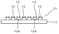
예비분리단계(S20)는 도 2 내지 6에 도시된 바와 같이 기판(11)상에 형성된 마이크로 LED(15)들 중 1차로 선택된 마이크로 LED(15A)만을 포토레지스트(21), 포토마스크(22), 노광장치 및 에칭 용액을 이용하여 기판(11)으로부터 일정 부분 분리시키는 단계로서, 도포단계(S21)와, 노광단계(S22)와, 제1제거단계(S23)와, 에칭단계(S24)와, 제2제거단계(S25)를 포함하여 구성된다.In the preliminary separation step (S20), only the
도포단계(S21)는 기판(11)상의 모든 마이크로 LED(15)를 감싸도록 기판(11)의 상부에 포토레지스트(21)를 도포한다.In the coating step (S21), the
노광단계(S22)는 도 2에 도시된 바와 같이 포토마스크(22) 및 노광장치를 이용하여 마이크로 LED(15)들 중에서 1차로 선택된 마이크로 LED(15A)를 감싸고 있는 포토레지스트(21)의 특정 영역(21A)을 제외한 나머지 영역만 선택적으로 노광시킨다.The exposure step (S22) is a specific area of the
포토레지스트(21)는 본래는 특수한 약품이나 용액 (Si 기판의 경우 KOH, GaAs 기판의 경우 HF)에 대하여 가용성이나 광에 노출되면 불용성이 되는 네거티브형과, 이와 반대로 본래는 특수한 약품이나 용액에 대하여 불용성이나 광에 노출되면 가용성으로 변화되는 포지티브형의 것을 적용할 수 있으나, 본 실시 예에서는 전자의 것을 적용하였으나, 후자의 것을 적용할 수 있음은 물론이다.The
제1제거단계(S23)는 마이크로 LED(15)들 중에서 1차로 선택된 마이크로 LED(15A)를 감싸는 포토레지스트(21)의 특정 영역(21A)을 제거 즉, 포토마스크(22)에 의해 광을 받지 않은 포토레지스트(21)의 특정 영역(21A)을 별도의 특수 약품 또는 용액을 이용하여 제거하여 1차로 선택된 마이크로 LED(15A)를 외부로 노출시킨다. 제1제거단계(S23)에서 적용되는 약품 또는 용액은 Tetramethylammonium hydroxide, ethyl lactate and diacetone alcohol 등을 이용할 수 있다.The first removing step (S23) removes a
에칭단계(S24)는 도 4에 도시된 바와 같이 에칭용액을 이용하여 마이크로 LED(15)들 중에서 1차로 선택된 마이크로 LED(15A)를 기판(11)으로부터 일정 부분 분리시키는 단계로서, 기판(11) 전체를 에칭용액에 침지시킨 후 CLO 방식으로 1차로 선택된 마이크로 LED(15A)와 기판(11)의 접합 부위를 에칭하여 1차로 선택된 마이크로 LED(15A)를 기판(11)으로부터 일정 부분 분리시킨다. The etching step (S24) is a step of separating a predetermined portion from the
도 4를 참조하면 1차로 선택된 마이크로 LED(15A)는 에칭단계(S24)를 통해 기판(11)과의 접합력이 본래의 접합력 대비 약 15%에 이르는 수준만 남아있도록 또는 약 85%의 접합력이 제거될 수 있다. 이때, 1차로 선택된 마이크로 LED(15A)를 제외한 나머지 마이크로 LED(15)는 포토레지스트(21)에 의해 보호되어 기판(11)에 대한 접합력이 제거 또는 약화되지 않는다. Referring to FIG. 4, the firstly selected
에칭단계(S24)에서 사용되는 에칭용액은 기판의 종류에 따라 수산화칼륨(KOH) 또는 불산(HF)을 적용할 수 있으며, Si 기판을 적용하는 경우에는 수산화칼륨(KOH)을 사용하고, GaAs 기판을 적용하는 경우에는 불산(HF)을 사용한다.As the etching solution used in the etching step (S24), potassium hydroxide (KOH) or hydrofluoric acid (HF) can be applied depending on the type of substrate, and potassium hydroxide (KOH) is used when applying a Si substrate, and a GaAs substrate When applying, hydrofluoric acid (HF) is used.
제2제거단계(S25)는 도 6에 도시된 바와 같이 마이크로 LED(15)들 중에서 1차로 선택된 마이크로 LED(15A) 이외의 나머지 마이크로 LED(15)를 감싸는 포토레지스트(21)의 나머지 영역을 완전히 제거하는 단계로서, 포토레지스트(21)의 나머지 영역은 아세톤과, 산소 플라즈마 처리, NMP(1-methyl-2-pyrrolidone)를 통해 제거할 수 있다.In the second removing step (S25), the remaining areas of the
제2제거단계(S25) 이후에는 도 7에 도시된 바와 같이 이전의 에칭단계(S24)에서 마이크로 LED(15)와 기판(11)과의 접합력을 본래의 접합력 대비 약 15%에 이르는 수준만 남아있도록 된 상태에서 마이크로 LED(15)와 기판(11)의 접합력을 약 5%에 이르는 수준만 남아있도록 접합력을 제거하는 에칭단계(S24)를 한 번 더 반복할 수 있다.After the second removal step (S25), as shown in FIG. 7, only a level of about 15% of the bonding force between the
그리고, 도 4 및 도 5에 도시된 바와 같이 예비분리단계(S20)의 에칭단계(S24)와 제2제거단계(S25) 사이에는 전극부형성단계와, 보호막형성단계를 더 포함할 수 있다.In addition, as shown in FIGS. 4 and 5, between the etching step S24 and the second removing step S25 of the preliminary separation step S20, an electrode part forming step and a protective film forming step may be further included.
전극부형성단계는 도 3의 제1제거단계(S23)를 통해 외부로 노출되는 1차 선택된 마이크로 LED(15)의 상부에 전극부(13)를 형성하는 단계로서, p형 반도체층에 ITO 등의 투명전극을 형성하고, 투명전극 상에 p형 전극을 형성하며, 식각단계에서 외부로 노출된 n형 반도체층에 n형 전극을 형성한다.The electrode part forming step is a step of forming the
그리고, 보호막형성단계는 마이크로 LED(15)의 상부를 보호하도록 전극부(13)를 제외한 마이크로 LED(15)의 상부를 보호막으로 감싸 보호막을 형성한다.In the protective film forming step, a protective film is formed by wrapping the upper portion of the
본 실시 예에 따른 마이크로 LED의 선택 전사방법의 마이크로 LED 제조단계(S10)에서 마이크로 LED(15)에 전극부(13)를 형성하지 않고, 예비분리단계(S20)의 에칭단계(S24)와 제2제거단계(S25) 사이에서 마이크로 LED(15)에 전극부(13)를 형성함으로써 에칭단계(S24)에서 기판(11)을 에칭용액에 침지시켜 에칭할 때, 전극부(13)가 에칭용액에 의해 손상되는 것을 방지할 수 있다.In the micro LED manufacturing step (S10) of the micro LED selection transfer method according to the present embodiment, without forming the
완전분리단계(S30)는 온도조건에 따라 점착력이 발생하거나 약화 또는 소멸되는 제1온도가변형 점착시트(31)에 기판(11)상의 마이크로 LED(15)들을 점착 및 고정시킨 후, 1차로 선택된 마이크로 LED(15A)만을 기판(11)으로부터 완전 분리시킨다.In the complete separation step (S30), after attaching and fixing the
완전분리단계(S30)는 도 8에 도시된 바와 같이 상온에서 기판(11)상의 마이크로 LED(15)가 제1온도가변형 점착시트(31)에 밀착되도록 기판(11)을 뒤집어 제1온도가변형 점착시트(31)에 밀착시키고, 도 9에 도시된 바와 같이 제1온도가변형 점착시트(31)에 점착력을 발생시켜 마이크로 LED(15)가 제1온도가변형 점착시트(31)에 점착 및 고정되도록 제1온도가변형 점착시트(31)의 온도를 조절하고, 기판(11)을 제1온도가변형 점착시트(31)에서 분리시킨다.The complete separation step (S30) is a first temperature-variable adhesive by turning the
완전분리단계(S30)에서 적용되는 제1온도가변형 점착시트(31)는 설정된 기준온도 이상에서는 점착력이 발생하고, 설정된 기준온도 이하에서는 점착력이 소멸되는 쿨-오프타입을 적용하며, 제1온도가변형 점착시트(31)에 밀착된 마이크로 LED(15A)가 제1온도가변형 점착시트(31)에 점착 및 고정되도록 제1온도가변형 점착시트(31)를 상온의 수준으로 가열한다.The first temperature-
상기 완전분리단계(S30)를 통해 1차로 선택된 마이크로 LED(15A)는 기판(11)으로부터 완전 분리됨과 동시에 제1온도가변형 점착시트(31)로 이동된다.The
전사단계(S40)는 도 10 내지 도 13에 도시된 바와 같이 기판(11)으로부터 제1온도가변형 점착시트(31)로 이동된 마이크로 LED(15A)를 타겟디바이스(40)에 전사시키는 단계로서, 제1전사단계(S41)와, 제2전사단계(S42)를 포함한다.The transfer step (S40) is a step of transferring the
제1전사단계(S41)는 도 10에 도시된 바와 같이 제1온도가변형 점착시트(31)상의 마이크로 LED(15A)가 또 다른 타입의 제2온도가변형 점착시트(32)에 밀착되도록 제1온도가변형 점착시트(31)를 뒤집어 제2온도가변형 점착시트(32)에 밀착시키고, 도 11에 도시된 바와 같이 마이크로 LED(15A)를 제2온도가변형 점착시트(32)로 이동시킬 수 있도록 마이크로 LED(15A)에 대한 제1온도가변형 점착시트(31)의 점착력은 소멸시키고 마이크로 LED(15A)에 대한 제2온도가변형 점착시트(32)의 점착력은 발생시킬 수 있도록 제1온도가변형 점착시트(31) 및 제2온도가변형 점착시트(32)의 온도를 각각 조절하며, 제1온도가변형 점착시트(31)를 제2온도가변형 점착시트(32)로부터 분리한다.The first transfer step (S41) is a first temperature so that the micro LED (15A) on the first temperature-
제1전사단계(S41)에서 적용되는 제2온도가변형 점착시트(32)는 설정된 기준온도(일 예로 상온 수준) 이상에서는 점착력이 약화되거나 소멸되고, 설정된 기준온도 이하에서는 점착력이 발생하는 웜-오프타입을 적용하며, 제1전사단계(S41)의 온도조정단계에서는 제2온도가변형 점착시트(32)에 밀착된 마이크로 LED(15A)가 제2온도가변형 점착시트(32)에 점착 및 고정되도록 제1온도가변형 점착시트 및 제2온도가변형 점착시트(32)를 설정된 기준온도 이하로 냉각시킨다.The second temperature-variable pressure-
도 11에 도시된 바와 같이 제1전사단계(S41)를 통해 제1온도가변형 점착시트(31)의 마이크로 LED(15A)는 제2온도가변형 점착시트(32)로 완전 이동된다.As shown in FIG. 11, the
그리고, 제2전사단계(S42)는 제1전사단계(S41)를 통해 제2온도가변형 점착시트(32)로 이동된 마이크로 LED(15A)를 타겟디바이스(40)로 이동시키는 단계로서, 도 12에 도시된 바와 같이 제2온도가변형 점착시트(32)로 이송된 마이크로 LED(15A)의 전극부(13)가 타겟디바이스(40)의 접합층(41)을 향하도록 제2온도가변형 점착시트(32)를 타겟디바이스(40)에 밀착시키고, 마이크로 LED(15A)에 대한 제2온도가변형 점착시트(32)의 점착력을 소멸시키도록 제2온도가변형 점착시트(32)의 온도를 조정하며, 도 13에 도시된 바와 같이 제2온도가변형 점착시트(32)를 타겟디바이스(40)로부터 분리함으로써 타겟디바이스(40)에 1차로 선택된 마이크로 LED(15A)의 전사 과정이 완료된다.And, the second transfer step (S42) is a step of moving the micro LED (15A) moved to the second temperature-
타겟디바이스에 형성되는 접합층은 1차로 선택된 마이크로 LED(15A)의 전극부(13)를 타겟디바이스 상에 형성되는 회로패턴에 접속 및 타겟디바이스에 접합시키기 위한 것으로서, 미세한 도전입자를 수지 내에 분산시키고, 두께 방향으로 가열 및 가압시 두께 방향으로만 도전이 이루어지도록 된 필름 형태의 이방성 도전 필름(Anisotropic Conductive Film; ACF) 또는 이방성 도전 접착제(Anisotropic Conductive Adhesive; ACA)를 적용할 수 있다. 이방성 도전 필름 또는 이방성 도전 접착제 내의 도전입자는 수 마이크로미터의 입도를 갖는 니켈, 카본, 솔더 볼 등이 적용될 수 있다.The bonding layer formed on the target device is for connecting the
제2전사단계(S42)에서는 타겟디바이스(40)의 접합층(41)에 밀착된 마이크로 LED(15)가 타겟디바이스(40)의 접합층(41)에 남아 있도록 제2온도가변형 점착시트(32)를 설정된 기준온도 이상 또는 상온 수준으로 가열한다.In the second transfer step (S42), the second temperature-
본 발명에 따른 마이크로 LED의 선택 전사방법의 전사단계(S40)를 제1전사단계(S41) 및 제2전사단계(S42)로 구분한 것은 완전분리단계(S30)를 통해 제1온도가변형 점착시트(31)로 이동된 마이크로 LED(15A)의 전극부(13)가 제1온도가변형 점착시트(31)에 점착 및 고정된 상태에서 마이크로 LED(15A)의 전극부(13)를 타겟디바이스(40)의 접합층(41)에 접합시키기 불가능하므로 이러한 문제를 해결하기 위해 마이크로 LED(15A)의 전극부(13)가 외측으로 노출되게 제1온도가변형 점착시트(31)로부터 제2온도가변형 점착시트(32)로 마이크로 LED(15A)를 한 번 더 이동시키는 구조를 적용하였다. 즉, 제2온도가변형 점착시트(32)를 통해 마이크로 LED(15A)의 전극부(13)를 타겟디바이스(40)의 접합층(41)에 밀착 및 접합시킬 수 있다.The transfer step (S40) of the micro LED selection transfer method according to the present invention is divided into a first transfer step (S41) and a second transfer step (S42) through a complete separation step (S30). In the state that the
그리고, 본 발명에 따른 마이크로 LED의 선택 전사방법은 기판(11)으로부터 타겟디바이스(40)로 1차 선택된 마이크로 LED(15A)의 전사가 완료된 후 즉, 전사단계(S40)가 완료된 이후에는 완전분리단계(S30) 후 기판(11)상에 남아 있는 마이크로 LED(15)들 중 2차 및 3차로 선택되는 마이크로 LED(15)를 각각 기판(11)으로부터 순차적으로 분리 및 타겟디바이스(40)에 순차적으로 전사시킬 수 있도록 도 2의 예비분리단계(S20)부터 완전분리단계(S30) 및 전사단계(S40)를 반복하는 반복단계(S50)를 더 포함한다.In addition, the micro LED selective transfer method according to the present invention is completely separated after the transfer of the first selected
상술한 바와 같은 본 발명의 제1실시 예에 따른 마이크로 LED의 선택 전사방법은 펨토초 레이저를 이용하여 마이크로 LED를 기판으로부터 타겟디바이스로 선택 전사시키는 종래의 전사방식에 비해 대면적 가공, 온도가변형 점착시트의 점착력 조절, 마이크로 LED의 전사를 매우 용이하게 할 수 있으며, 레이저를 사용하지 않으므로 점착시트의 버닝 현상 및 마이크로 LED의 손상이 적은 장점이 있다.As described above, the micro LED selective transfer method according to the first embodiment of the present invention uses a femtosecond laser to selectively transfer the micro LED from the substrate to the target device, compared to the conventional transfer method, which is a large area processing, temperature-variable adhesive sheet. It can be very easy to control the adhesion of the micro LED and transfer of the micro LED, and since it does not use a laser, there is an advantage of less burning of the adhesive sheet and less damage to the micro LED.
한편, 도 14 내지 도 26에는 본 발명의 제2실시 예에 따른 마이크로 LED의 선택 전사방법이 도시되어 있다.Meanwhile, FIGS. 14 to 26 illustrate a method of selectively transferring a micro LED according to a second embodiment of the present invention.
도 14 내지 도 26을 참조하면, 본 발명의 제2실시 예에 따른 마이크로 LED의 선택 전사방법은 마이크로 LED 제조단계(S10)와, 예비분리단계(S20)와, 완전분리단계(S30)와, 전사단계(S40)를 포함하여 구성된다.14 to 26, the selective transfer method of the micro LED according to the second embodiment of the present invention includes a micro LED manufacturing step (S10), a preliminary separation step (S20), a complete separation step (S30), It comprises a transfer step (S40).
본 발명의 제2실시 예에 따른 마이크로 LED의 선택 전사방법은 앞서 도 1 내지 도 13을 참조하여 설명한 본 발명의 제1실시 예에 따른 마이크로 LED의 선택 전사방법과 반도체구조물 또는 마이크로 LED에 전극부와 보호막을 형성하기 위한 전극부형성단계와, 보호막형성단계의 순서만 다를 뿐 그 이외의 나머지 방법은 본 발명의 제1실시 예에 따른 마이크로 LED의 선택 전사방법과 동일하다.The method for selectively transferring micro LEDs according to the second embodiment of the present invention includes a method for selectively transferring micro LEDs according to the first embodiment of the present invention described with reference to FIGS. 1 to 13 and an electrode part to a semiconductor structure or micro LED. The order of the electrode part forming step for forming the protective layer and the protective layer forming step is different, but the other methods are the same as the selective transfer method of the micro LED according to the first embodiment of the present invention.
본 발명의 제2실시 예에 따른 마이크로 LED의 선택 전사방법의 전극부형성단계 및 보호막형성단계는 도 1 내지 도 13을 참조하여 설명한 본 발명의 제1실시 예에 따른 마이크로 LED의 선택 전사방법의 예비분리단계(S20)의 에칭단계(S24)와 제2제거단계(S25) 사이에서 수행하지 않고, 예비분리단계(S20) 이전의 마이크로 LED 제조단계(S10)의 식각단계 이후에 수행한다.The electrode part forming step and the protective film forming step of the method for selectively transferring micro LEDs according to the second embodiment of the present invention are described with reference to FIGS. 1 to 13 in the method for selectively transferring micro LEDs according to the first embodiment of the present invention. It is not performed between the etching step (S24) and the second removing step (S25) of the preliminary separation step (S20), but is performed after the etching step of the micro LED manufacturing step (S10) before the preliminary separation step (S20).
전극부형성단계에서는 마이크로 LED 제조단계(S10)의 식각단계 이후에 p형 반도체 상에 형성되는 p형 전극, 식각단계를 통해 외부로 노출된 n형 반도체 상에 형성되는 n형 전극, 반사 전극 및 투명 전극을 포함하는 전극부(13)를 마이크로 LED(15) 상에 형성한다. In the electrode part formation step, a p-type electrode formed on the p-type semiconductor after the etching step of the micro LED manufacturing step (S10), an n-type electrode formed on the n-type semiconductor exposed to the outside through the etching step, a reflective electrode, and An
그리고, 보호막형성단계는 전극부(13)가 형성된 마이크로 LED(15)의 상부를 보호하도록 전극부(13)를 제외한 마이크로 LED(15)의 상부를 보호막으로 감싸 보호막을 형성한다.In the protective film forming step, a protective film is formed by wrapping the upper portion of the
앞서 설명한 본 발명의 제1실시 예에 따른 마이크로 LED의 선택 전사방법은 도 4 및 도 5에 도시된 바와 같이 전극부형성단계와, 보호막형성단계가 예비분리단계에서 형성되지만 본 발명의 제2실시 예에 따른 마이크로 LED의 선택 전사방법의 전극부형성단계와, 보호막형성단계는 도 14에 도시된 바와 같이 마이크로 LED 제조단계(S10)에서 미리 수행되므로 도 16 내지 도 18의 예비분리단계 즉, 1차 선택된 마이크로 LED를 외부로 노출시키는 제1제거단계 이후에 전극부 및 보호막을 형성하는 단계가 생략된 것이 본 발명의 제1실시 예에 따른 마이크로 LED의 선택 전사방법과는 다르다.In the method of selective transfer of micro LEDs according to the first embodiment of the present invention described above, as shown in FIGS. 4 and 5, the electrode part forming step and the protective film forming step are formed in the preliminary separation step, but the second embodiment of the present invention Since the electrode part formation step and the protective film formation step of the selection transfer method of the micro LED according to the example are performed in advance in the micro LED manufacturing step (S10) as shown in FIG. 14, the preliminary separation step of FIGS. It is different from the selective transfer method of the micro LED according to the first embodiment of the present invention in that the step of forming the electrode part and the protective film after the first removing step of exposing the secondary selected micro LED to the outside is omitted.
마이크로 LED 제조단계(S10)는 기판(11)상에 p형 반도체층, n형 반도체층 및 활성층을 포함하는 반도체구조물(이하, 마이크로 LED(15))을 형성하는 반도체구조물형성단계와, 마이크로 LED(15) 내부의 p형 반도체층 또는 n형 반도체층의 일부를 외부로 노출시키도록 마이크로 LED(15)의 일부를 식각하여 메사 구조부를 형성하는 식각단계를 포함하여 마이크로 LED(15)를 제조한다.Micro LED manufacturing step (S10) includes a semiconductor structure forming step of forming a semiconductor structure (hereinafter, micro LED 15) including a p-type semiconductor layer, an n-type semiconductor layer and an active layer on the
예비분리단계(S20)는 도 15 내지 20에 도시된 바와 같이 기판(11)상에 형성된 마이크로 LED(15)들 중 1차로 선택된 마이크로 LED(15A)만을 포토레지스트(21), 포토마스크(22), 노광장치 및 에칭 용액을 이용하여 기판(11)으로부터 일정 부분 분리시키는 단계로서, 도포단계(S21)와, 노광단계(S22)와, 제1제거단계(S23)와, 에칭단계(S24)와, 제2제거단계(S25)를 포함하여 구성된다.In the preliminary separation step (S20), only the
도포단계(S21)는 15에 도시된 바와 같이 기판(11)상의 모든 마이크로 LED(15)를 감싸도록 기판(11)의 상부에 포토레지스트(21)를 도포한다.In the coating step (S21), as shown in FIG. 15, a
노광단계(S22)는 도 16에 도시된 바와 같이 포토마스크 및 노광장치를 이용하여 마이크로 LED(15)들 중에서 1차로 선택된 마이크로 LED(15A)를 감싸고 있는 포토레지스트(21)의 특정 영역(21A)을 제외한 나머지 영역만 선택적으로 노광시킨다.The exposure step (S22) is a
포토레지스트(21)는 본래는 특수한 약품이나 용액에 대하여 가용성이나 광에 노출되면 불용성이 되는 네거티브형과, 이와 반대로 본래는 특수한 약품이나 용액에 대하여 불용성이나 광에 노출되면 가용성으로 변화되는 포지티브형의 것을 적용할 수 있으나, 본 실시 예에서는 전자의 것을 적용하였으나, 후자의 것을 적용할 수 있음은 물론이다.The
제1제거단계(S23)는 도 17에 도시된 바와 같이 마이크로 LED(15)들 중에서 1차로 선택된 마이크로 LED(15A)를 감싸는 포토레지스트(21)의 특정 영역(21A)을 제거 즉, 포토마스크(22)에 의해 광을 받지 않은 포토레지스트(21)의 특정 영역(21A)을 별도의 특수 약품 또는 용액을 이용하여 제거하여 1차로 선택된 마이크로 LED(15A)를 외부로 노출시킨다. 제1제거단계(S23)에서 적용되는 약품 또는 용액은 Tetramethylammonium hydroxide, ethyl lactate and diacetone alcohol 등을 이용할 수 있다.The first removing step (S23) removes a
에칭단계(S24)는 도 18에 도시된 바와 같이 에칭용액을 이용하여 마이크로 LED(15)들 중에서 1차로 선택된 마이크로 LED(15A)를 기판(11)으로부터 일정 부분 분리시키는 단계로서, 기판(11) 전체를 에칭용액에 침지시킨 후 CLO 방식으로 1차로 선택된 마이크로 LED(15A)와 기판(11)의 접합 부위를 에칭하여 1차로 선택된 마이크로 LED(15A)를 기판(11)으로부터 일정 부분 분리시킨다. The etching step (S24) is a step of separating a predetermined portion from the
도 18을 참조하면 1차로 선택된 마이크로 LED(15A)는 에칭단계(S24)를 통해 기판(11)과의 접합력이 본래의 접합력 대비 약 15%에 이르는 수준만 남아있도록 또는 약 85%의 접합력이 제거될 수 있다. 이때, 1차로 선택된 마이크로 LED(15A)를 제외한 나머지 마이크로 LED(15)는 포토레지스트(21)에 의해 보호되어 기판(11)에 대한 접합력이 제거 또는 약화되지 않는다. Referring to FIG. 18, the firstly selected micro LED (15A) is removed so that only about 15% of the bonding force with the
에칭단계(S24)에서 사용되는 에칭용액은 기판의 종류에 따라 수산화칼륨(KOH) 또는 불산(HF)을 적용할 수 있으며, Si 기판을 적용하는 경우에는 수산화칼륨(KOH)을 사용하고, GaAs 기판을 적용하는 경우에는 불산(HF)을 사용한다.As the etching solution used in the etching step (S24), potassium hydroxide (KOH) or hydrofluoric acid (HF) can be applied depending on the type of substrate, and potassium hydroxide (KOH) is used when applying a Si substrate, and a GaAs substrate When applying, hydrofluoric acid (HF) is used.
제2제거단계(S25)는 도 18 및 도 19에 도시된 바와 같이 마이크로 LED(15)들 중에서 1차로 선택된 마이크로 LED(15A) 이외의 나머지 마이크로 LED(15)를 감싸는 포토레지스트(21)의 나머지 영역을 완전히 제거하는 단계로서, 포토레지스트(21)의 나머지 영역은 아세톤과, 산소 플라즈마 처리, NMP(1-methyl-2-pyrrolidone)를 통해 제거할 수 있다.The second removal step (S25) is the rest of the
제2제거단계(S25) 이후에는 도 20에 도시된 바와 같이 이전의 에칭단계(S24)에서 마이크로 LED(15)와 기판(11)과의 접합력을 본래의 접합력 대비 약 15%에 이르는 수준만 남아있도록 된 상태에서 마이크로 LED(15)와 기판(11)의 접합력을 약 5%에 이르는 수준만 남아있도록 접합력을 제거하는 에칭단계(S24)를 한 번 더 반복할 수 있다.After the second removal step (S25), as shown in FIG. 20, only a level of about 15% of the bonding force between the
완전분리단계(S30)는 온도조건에 따라 점착력이 발생하거나 약화 또는 소멸되는 제1온도가변형 점착시트(31)에 기판(11)상의 마이크로 LED(15)들을 점착 및 고정시킨 후, 1차로 선택된 마이크로 LED(15A)만을 기판(11)으로부터 완전 분리시킨다.In the complete separation step (S30), after attaching and fixing the
완전분리단계(S30)는 도 21에 도시된 바와 같이 상온에서 기판(11)상의 마이크로 LED(15)가 제1온도가변형 점착시트(31)에 밀착되도록 기판(11)을 뒤집어 제1온도가변형 점착시트(31)에 밀착시키고, 제1온도가변형 점착시트(31)에 점착력을 발생시켜 마이크로 LED(15)가 제1온도가변형 점착시트(31)에 점착 및 고정되도록 제1온도가변형 점착시트(31)의 온도를 조절하고, 도 22에 도시된 바와 같이 기판(11)을 제1온도가변형 점착시트(31)에서 분리시킨다.The complete separation step (S30) is a first temperature-variable adhesive by turning the
완전분리단계(S30)에서 적용되는 제1온도가변형 점착시트(31)는 설정된 기준온도 이상에서는 점착력이 발생하고, 설정된 기준온도 이하에서는 점착력이 소멸되는 쿨-오프타입을 적용하며, 제1온도가변형 점착시트(31)에 밀착된 마이크로 LED(15A)가 제1온도가변형 점착시트(31)에 점착 및 고정되도록 제1온도가변형 점착시트(31)를 상온의 수준으로 가열한다.The first temperature-
상기 완전분리단계(S30)를 통해 1차로 선택된 마이크로 LED(15A)는 기판(11)으로부터 완전 분리됨과 동시에 제1온도가변형 점착시트(31)로 이동된다.The
전사단계(S40)는 도 23 내지 도 26에 도시된 바와 같이 기판(11)으로부터 제1온도가변형 점착시트(31)로 이동된 마이크로 LED(15A)를 타겟디바이스(40)에 전사시키는 단계로서, 제1전사단계(S41)와, 제2전사단계(S42)를 포함한다.The transfer step (S40) is a step of transferring the
제1전사단계(S41)는 도 23에 도시된 바와 같이 제1온도가변형 점착시트(31)상의 마이크로 LED(15A)가 또 다른 타입의 제2온도가변형 점착시트(32)에 밀착되도록 제1온도가변형 점착시트(31)를 뒤집어 제2온도가변형 점착시트(32)에 밀착시키고, 마이크로 LED(15A)를 제2온도가변형 점착시트(32)로 이동시킬 수 있도록 마이크로 LED(15A)에 대한 제1온도가변형 점착시트(31)의 점착력은 소멸시키고 마이크로 LED(15A)에 대한 제2온도가변형 점착시트(32)의 점착력은 발생시킬 수 있도록 제1온도가변형 점착시트(31) 및 제2온도가변형 점착시트(32)의 온도를 각각 조절하며, 도 24에 도시된 바와 같이 제1온도가변형 점착시트(31)를 제2온도가변형 점착시트(32)로부터 분리한다.The first transfer step (S41) is a first temperature so that the micro LED (15A) on the first temperature-
제1전사단계(S41)에서 적용되는 제2온도가변형 점착시트(32)는 설정된 기준온도(일 예로 상온 수준) 이상에서는 점착력이 약화되거나 소멸되고, 설정된 기준온도 이하에서는 점착력이 발생하는 웜-오프타입을 적용하며, 제1전사단계(S41)의 온도조정단계에서는 제2온도가변형 점착시트(32)에 밀착된 마이크로 LED(15A)가 제2온도가변형 점착시트(32)에 점착 및 고정되도록 제1온도가변형 점착시트 및 제2온도가변형 점착시트(32)를 설정된 기준온도 이하로 냉각시킨다.The second temperature-variable pressure-
도 24에 도시된 바와 같이 제1전사단계(S41)를 통해 제1온도가변형 점착시트(31)의 마이크로 LED(15A)는 제2온도가변형 점착시트(32)로 완전 이동된다.As shown in FIG. 24, the
그리고, 제2전사단계(S42)는 제1전사단계(S41)를 통해 제2온도가변형 점착시트(32)로 이동된 마이크로 LED(15A)를 타겟디바이스(40)로 이동시키는 단계로서, 도 25에 도시된 바와 같이 제2온도가변형 점착시트(32)로 이송된 마이크로 LED(15A)의 전극부(13)가 타겟디바이스(40)의 접합층(41)을 향하도록 제2온도가변형 점착시트(32)를 타겟디바이스(40)에 밀착시키고, 마이크로 LED(15A)에 대한 제2온도가변형 점착시트(32)의 점착력을 소멸시키도록 제2온도가변형 점착시트(32)의 온도를 조정하며, 도 26에 도시된 바와 같이 제2온도가변형 점착시트(32)를 타겟디바이스(40)로부터 분리함으로써 타겟디바이스(40)에 1차로 선택된 마이크로 LED(15A)의 전사 과정이 완료된다.And, the second transfer step (S42) is a step of moving the micro LED (15A) moved to the second temperature-
제2전사단계(S42)에서는 타겟디바이스(40)의 접합층(41)에 밀착된 마이크로 LED(15)가 타겟디바이스(40)의 접합층(41)에 남아 있도록 제2온도가변형 점착시트(32)를 설정된 기준온도 이상 또는 상온 수준으로 가열한다.In the second transfer step (S42), the second temperature-
본 발명에 따른 마이크로 LED의 선택 전사방법의 전사단계(S40)를 제1전사단계(S41) 및 제2전사단계(S42)로 구분한 것은 완전분리단계(S30)를 통해 제1온도가변형 점착시트(31)로 이동된 마이크로 LED(15A)의 전극부(13)가 제1온도가변형 점착시트(31)에 점착 및 고정된 상태에서 마이크로 LED(15A)의 전극부(13)를 타겟디바이스(40)의 접합층(41)에 접합시키기 불가능하므로 이러한 문제를 해결하기 위해 마이크로 LED(15A)의 전극부(13)가 외측으로 노출되게 제1온도가변형 점착시트(31)로부터 제2온도가변형 점착시트(32)로 마이크로 LED(15A)를 한 번 더 이동시키는 구조를 적용하였다. 즉, 제2온도가변형 점착시트(32)를 통해 마이크로 LED(15A)의 전극부(13)를 타겟디바이스(40)의 접합층(41)에 밀착 및 접합시킬 수 있다.The transfer step (S40) of the micro LED selection transfer method according to the present invention is divided into a first transfer step (S41) and a second transfer step (S42) through a complete separation step (S30). In the state that the
그리고, 본 발명에 따른 마이크로 LED의 선택 전사방법은 기판(11)으로부터 타겟디바이스(40)로 1차 선택된 마이크로 LED(15A)의 전사가 완료된 후 즉, 전사단계(S40)가 완료된 이후에는 완전분리단계(S30) 후 기판(11)상에 남아 있는 마이크로 LED(15)들 중 2차 및 3차로 선택되는 마이크로 LED(15)를 각각 기판(11)으로부터 순차적으로 분리 및 타겟디바이스(40)에 순차적으로 전사시킬 수 있도록 예비분리단계(S20)와, 완전분리단계(S30)와, 전사단계(S40)를 반복하는 반복단계(S50)를 더 포함한다.In addition, the micro LED selective transfer method according to the present invention is completely separated after the transfer of the first selected
한편, 도 27 내지 도 38에는 본 발명의 제3 실시 예에 따른 마이크로 LED의 선택 전사방법이 도시되어 있다. 도 내지 도 38을 참조하면, 본 발명의 제3 실시 예에 따른 마이크로 LED의 선택 전사방법은 마이크로 LED 제조단계(S100)와, 예비분리단계(S200)와, 완전분리단계(S300)와, 전사단계(S400)를 포함하여 구성된다.On the other hand, Figures 27 to 38 illustrate a method of selectively transferring a micro LED according to a third embodiment of the present invention. Referring to Figures to 38, the selective transfer method of the micro LED according to the third embodiment of the present invention is a micro LED manufacturing step (S100), a preliminary separation step (S200), a complete separation step (S300), and transfer It is configured including a step (S400).
마이크로 LED 제조단계(S100)는 기판(11)상에 마이크로 LED(15)을 형성하는 마이크로 LED형성단계와, 마이크로 LED(15) 내부의 반도체층 일부가 외부로 노출되도록 마이크로 LED(15)의 일부를 식각하는 식각단계와, 마이크로 LED(15)의 상부에 전극부(13)를 형성하는 전극부형성단계와, 마이크로 LED(15)의 상부를 보호하도록 전극부(13)를 제외한 마이크로 LED(15)의 상부를 보호막으로 감싸 보호막을 형성하는 보호막형성단계를 단계를 포함한다. Micro LED manufacturing step (S100) is a micro LED forming step of forming the
전극부형성단계와, 보호막형성단계는 마이크로 LED 제조단계(S100)에서 수행할 수도 있으나, 본 발명의 제1실시 예에 따른 마이크로 LED의 선택 전사방법의 예비분리단계(S20)와 같이 에칭 용액에 의한 전극부(13)의 손상을 방지할 수 있도록 기판(11) 상의 마이크로 LED(15)를 에칭용액을 이용하여 기판(11)으로부터 일정 부분 분리시키는 예비분리단계(S200)에서 수행할 수 있음은 물론이다.The electrode part forming step and the protective film forming step may be performed in the micro LED manufacturing step (S100), but in the etching solution as in the preliminary separation step (S20) of the selective transfer method of the micro LED according to the first embodiment of the present invention. The
예비분리단계(S200)는 기판(11)상의 모든 마이크로 LED(15)를 에칭 용액을 이용하여 기판(11)으로부터 일정 부분 분리시키도록 에칭 용액에 기판(11)을 침지시킨다. 예비분리단계(S200)에서는 본 발명의 제1실시 예에 따른 마이크로 LED의 선택 전사방법의 에칭단계(S24) 및 도 28에 도시된 바와 같이 마이크로 LED(15)와 기판(11)과의 접합력을 상호 간의 본래 접합력 대비 약 15% 내지 5%에 이르는 수준만 유지되게 또는 약 85%~95%를 제거할 수 있다.In the preliminary separation step (S200), the
완전분리단계(S300)는 온도조건에 따라 점착력이 발생하거나 약화 또는 소멸되는 온도가변형 점착시트 및 특정 패턴으로 형성되고 PET로 이루어진 마스크를 이용하여 기판(11)상의 마이크로 LED(15)들 중에서 1차로 선택된 마이크로 LED(15A)만을 온도가변형 점착시트에 점착 및 고정시킨 후에 1차로 선택된 마이크로 LED(15A)만을 기판(11)으로부터 완전 분리시킨다.The complete separation step (S300) is a first among
완전분리단계(S300)는 박막형성단계(S301)와, 마스크형성단계(S302)와, 마스크이송단계(S303)와, 선택분리단계(S304)를 포함하여 구성된다.The complete separation step (S300) includes a thin film forming step (S301), a mask forming step (S302), a mask transferring step (S303), and a selective separation step (S304).
박막형성단계(S301)는 도 29에 도시된 바와 같이 제1온도가변형 점착시트(31)를 준비하고, 제1온도가변형 점착시트(31) 상에 PET를 매우 얇게 도포하여 PET 박막층(35)을 형성한다.In the thin film forming step (S301), as shown in FIG. 29, a first temperature-
마스크형성단계(S302)는 도 30에 도시된 바와 같이 1차로 타겟디바이스(40)로 전사시키고자 하는 마이크로 LED(15A) 즉, 1차로 선택되는 마이크로 LED(15A)의 위치 및 배치에 대응되는 특정 패턴으로 PET 박막층(35)을 레이저 가공하여 특정 패턴의 PET 마스크(36)를 형성한다.In the mask forming step (S302), as shown in FIG. 30, the
마스크이송단계(S303)는 도 31에 도시된 바와 같이 제2온도가변형 점착시트(32)를 준비하고, 제1온도가변형 점착시트(31)를 뒤집어 제1온도가변형 점착시트(31)상의 PET 마스크(36)를 제2온도가변형 점착시트(32)에 밀착시키며, 제1온도가변형 점착시트(31)의 점착력은 소멸 또는 약화되고 제2온도가변형 점착시트(32)의 점착력은 발생하도록 제1온도가변형 점착시트(31) 및 제2온도가변형 점착시트(32)의 온도를 각각 조절하며, PET 마스크(36)가 제2온도가변형 점착시트(32)에 점착 및 고정된 상태에서 도 32에 도시된 바와 같이 제1온도가변형 점착시트(31)를 제2온도가변형 점착시트(32)로부터 분리하여 PET 마스크(36)를 제2온도가변형 점착시트(32)로 완전 이송시킨다.In the mask transfer step (S303), as shown in FIG. 31, a second temperature-
마스크이송단계(S303)의 제1온도가변형 점착시트(31)는 설정된 기준온도(일 예로 상온 수준) 이상에서는 점착력이 약화되거나 소멸되고, 설정된 기준온도 이하에서는 점착력이 발생하는 웜-오프타입을 적용하고, 제2온도가변형 점착시트(32)는 설정된 기준온도 이상에서는 점착력이 발생하고, 설정된 기준온도 이하에서는 점착력이 소멸되는 쿨-오프타입을 적용하였다. 이와 다르게 제1온도가변형 점착시트(31)를 웜-오프타입으로 적용하고, 제2온도가변형 점착시트(32)를 쿨-오프 타입으로 적용할 수 있음은 물론이다.The first temperature-variable pressure-
선택분리단계(S304)는 도 33에 도시된 바와 같이 예비분리단계(S200)를 통해 기판(11)으로부터 일정 부분 분리된 마이크로 LED(15)를 PET 마스크(36)가 점착된 영역을 제외한 제2온도가변형 점착시트(32) 상에 점착 및 고정시키도록 제2온도가변형 점착시트(32)와 기판(11)을 서로 밀착시키고, 제2온도가변형 점착시트(32)에 점착력이 발생하도록 제2온도가변형 점착시트(32)의 온도를 조정하며, 마이크로 LED(15A)가 제2온도가변형 점착시트(32)에 점착 및 고정된 후 도 34에 도시된 바와 같이 제2온도가변형 점착시트(32)로부터 기판(11)을 분리하여 기판(11)으로부터 마이크로 LED(15)를 완전 분리시킨다.In the selective separation step (S304), the
선택분리단계(S304)를 통해 PET 마스크(36)에 의해 1차로 선택된 마이크로 LED(15A)가 기판(11)으로부터 완전 분리 및 제2온도가변형 점착시트(32)로 완전 이동된다.Through the selective separation step (S304), the
전사단계(S400)는 기판(11)으로부터 제2온도가변형 점착시트(32)로 이동된 마이크로 LED(15)를 타겟디바이스(40)에 전사시는 단계로, 제1전사단계(S410)와 제2전사단계(S420)를 포함한다.Transfer step (S400) is a step of transferring the
제1전사단계(S410)는 35에 도시된 바와 같이 제2온도가변형 점착시트(32)에 점착 및 고정된 마이크로 LED(15) 및 PET 마스크(36)를 제3온도가변형 점착시트(33)로 이송시키는 단계로서, 제2온도가변형 점착시트(32)를 제3온도가변형 점착시트(33)에 밀착시킨다. In the first transfer step (S410), the
그리고, 제2온도가변형 점착시트(32)의 점착력이 약화 또는 소멸되도록 제2온도가변형 점착시트(32)의 온도를 조절 및 제3온도가변형 점착시트(33)의 점착력이 발생하도록 제3온도가변형 점착시트(33)의 온도를 조절한다. In addition, the temperature of the second temperature-variable pressure-
제3온도가변형 점착시트(33)에 마이크로 LED(15) 및 PET 마스크(36)가 점착 및 고정된 후에는 제2온도가변형 점착시트(32)를 제3온도가변형 점착시트(33)로부터 분리시킨다. After the
도 36에 도시된 바와 같이 제1전사단계(S410)를 통해 제2온도가변형 점착시트(32)상의 마이크로 LED(15A) 및 PET 마스크(36)가 제3온도가변형 점착시트(33)로 이송된다.As shown in FIG. 36, the
제2전사단계(S420)는 제3온도가변형 점착시트(33)에 점착 및 고정된 마이크로 LED(15)를 타겟디바이스(40)로 전사시키는 단계로서, 도 37에 도시된 바와 같이 제3온도가변형 점착시트(33)상의 마이크로 LED(15A)의 전극부(13)가 타겟디바이스(40)상에 구비된 접합층(41)에 접합되도록 제3온도가변형 점착시트(33)를 타겟디바이스(40)에 밀착시키고, 제3온도가변형 점착시트(33)의 점착력이 약화 또는 소멸되도록 제3온도가변형 점착시트(33)의 온도를 조절한다. 그리고, 마이크로 LED(15A)의 전극부(13)가 타겟디바이스(40)의 접합층(41)에 접합된 후에는 도 38에 도시된 바와 같이 제3온도가변형 점착시트(33)를 타겟디바이스(40)로부터 분리시킨다. The second transfer step (S420) is a step of transferring the
제2전사단계(S420)를 통해 제3온도가변형 점착시트(33)상의 마이크로 LED(15)가 타겟디바이스(40)로 전사된다.Through the second transfer step (S420), the
제2전사단계(S420)에서 적용되는 제3온도가변형 점착시트(33) 앞서 설명한 제1온도가변형 점착시트(31)와 마찬가지로 설정된 기준온도(일 예로 상온 수준) 이상에서는 점착력이 약화되거나 소멸되고, 설정된 기준온도 이하에서는 점착력이 발생하는 웜-오프타입을 적용한다.The third temperature-variable pressure-
본 실시 예에 따른 마이크로 LED의 선택 전사방법의 전사단계(S400)를 제1전사단계(S410) 및 제2전사단계(S420)로 구분한 것은, 완전분리단계(S300)를 통해 제2온도가변형 점착시트(32)로 이동된 마이크로 LED(15A)의 전극부(13)가 제2온도가변형 점착시트(32)에 점착 및 고정된 상태에서 마이크로 LED(15A)의 전극부(13)를 타겟디바이스(40)의 접합층(41)에 접합시키기 불가능하므로 이러한 문제를 해결하기 위해 마이크로 LED(15A)의 전극부(13)가 외측으로 노출되게 제2온도가변형 점착시트(32)로부터 제3온도가변형 점착시트(33)로 마이크로 LED(15A)를 한 번 더 이동시키는 구조를 적용하였다. 즉, 제3온도가변형 점착시트(33)를 통해 마이크로 LED(15A)의 전극부(13)를 타겟디바이스(40)의 접합층(41)에 밀착 및 접합시킬 수 있다.The transfer step (S400) of the micro LED selection transfer method according to the present embodiment is divided into a first transfer step (S410) and a second transfer step (S420), and the second temperature is changed through the complete separation step (S300). When the
또한, 전사단계(S400)에서는 제2온도가변형 점착시트(32)로부터 제3온도가변형 점착시트(33)로 마이크로 LED(15A)를 이동시킬 때, PET 마스크(36)가 함께 제2온도가변형 점착시트(32)로부터 제3온도가변형 점착시트(33)로 이동시키는 구조를 적용하였으나, 이와 다르게 PET 마스크(36)를 제외하고 마이크로 LED(15)만 이동시킬 수 있음은 물론이다.In addition, in the transfer step (S400), when moving the
그리고, 본 실시 예에 따른 마이크로 LED의 선택 전사방법은 기판(11)으로부터 타겟디바이스(40)로 1차 선택된 마이크로 LED(15A)의 전사가 완료된 후 즉, 전사단계(S400)가 완료된 이후에는 완전분리단계(S300) 후 기판(11)상에 남아 있는 마이크로 LED(15)들 중 2차 및 3차로 선택되는 마이크로 LED(15)를 각각 기판(11)으로부터 순차적으로 분리 및 타겟디바이스(40)에 순차적으로 전사시킬 수 있도록 완전분리단계(S300)와, 전사단계(S400)를 반복하는 반복단계(S500)를 더 포함한다.In addition, the micro LED selection transfer method according to the present embodiment is complete after the transfer of the
이 경우, 제2전사단계(S420)에서 사용되고 1차 선택된 마이크로 LED(15A)가 완전히 분리된 상태의 제3온도가변형 점착시트(33)는 PET 마스크(36)가 제3온도가변형 점착시트(33) 상에 그대로 부착 및 유지되어 있고, 제1온도가변형 점착시트(31)와 제3온도가변형 점착시트(32)가 온도 조건에 대한 특성이 동일하므로 반복단계(S500)에서는 앞서 설명한 완전분리단계(S300)의 도 29 내지 도 30에 도시된 박막형성단계(S301) 및 마스크형성단계(S302)를 생략할 수 있으며, 제3온도가변형 점착시트(33)는 도 31에 도시된 바와 같이 마스크이송단계(S303)에서 제1온도가변형 점착시트(31)을 대신하여 재사용할 수 있다.In this case, the third temperature-
이상에서 설명한 본 발명에 따른 마이크로 LED의 선택 전사방법은 첨부된 도면을 참조로 설명하였으나 이는 예시적인 것에 불과하며, 당해 기술분야에서 통상의 지식을 가진 자라면 이로부터 다양한 변형 및 균등한 타 실시 예가 가능하다는 점을 이해할 것이다. The selection and transfer method of the micro LED according to the present invention described above has been described with reference to the accompanying drawings, but this is only illustrative, and various modifications and other equivalent embodiments are provided from those of ordinary skill in the art. You will understand that it is possible.
따라서, 본 발명의 진정한 기술적 보호의 범위는 첨부된 청구범위의 기술적 사상에 의해서만 정해져야 할 것이다.Therefore, the scope of the true technical protection of the present invention should be determined only by the technical spirit of the appended claims.
11 : 기판
13 : 전극부
15 : 마이크로 LED
15A : 1차 선택된 마이크로 LED
21 : 포토레지스트
22 : 포토마스크
31 : 제1온도가변형 점착시트
32 : 제2온도가변형 점착시트
33 : 제3온도가변형 점착시트
40 : 타겟디바이스
41 : 접합층
S10 : 마이크로 LED 제조단계
S20 : 예비분리단계
S21 : 도포단계
S22 : 노광단계
S23 : 제1제거단계
S24 : 에칭단계
S25 : 제2제거단계
S30 : 완전분리단계
S40 : 전사단계
S41 : 제1전사단계
S42 : 제2전사단계11: substrate
13: electrode part
15: Micro LED
15A: Primary selected micro LED
21: photoresist
22: photo mask
31: the first temperature-variable adhesive sheet
32: second temperature variable adhesive sheet
33: 3rd temperature variable adhesive sheet
40: target device
41: bonding layer
S10: Micro LED manufacturing step
S20: Preliminary separation step
S21: Application step
S22: Exposure step
S23: First removal step
S24: etching step
S25: second removal step
S30: Complete separation step
S40: Warrior stage
S41: First Warrior Stage
S42: 2nd Warrior Stage
Claims (6)
상기 기판상의 모든 마이크로 LED를 에칭 용액을 이용하여 상기 기판으로부터 일정 부분 분리시키는 예비분리단계와;
온도조건에 따라 점착력이 발생하거나 약화 또는 소멸되는 제2온도가변형 점착시트와 상기 제2온도가변형 점착시트상에 특정 패턴으로 형성되고 PET로 이루어진 마스크를 이용하여 상기 기판상의 마이크로 LED들 중에서 1차로 선택된 마이크로 LED만을 상기 제2온도가변형 점착시트에 점착 및 고정시킨 후에 1차로 선택된 마이크로 LED만을 상기 기판으로부터 완전 분리시키는 완전분리단계와;
상기 기판으로부터 상기 제2온도가변형 점착시트로 이동된 마이크로 LED를 타겟디바이스에 전사시키는 전사단계;를 포함하며,
상기 전사단계 이후에는 상기 완전분리단계 후 상기 기판상에 남아 있는 마이크로 LED들 중 2차 및 3차로 선택되는 마이크로 LED를 각각 상기 기판으로부터 순차적으로 분리 및 상기 타겟디바이스에 순차적으로 전사시킬 수 있도록 상기 완전분리단계와, 상기 전사단계를 반복하는 반복단계를 더 포함하고,
상기 전사단계는
상기 제2온도가변형 점착시트 상의 마이크로 LED를 제3온도가변형 점착시트로 이동시키도록 상기 제2온도가변형 점착시트를 제3온도가변형 점착시트에 밀착시키고, 상기 제2온도가변형 점착시트 및 상기 제3온도가변형 점착시트의 온도를 조절하며, 상기 제2온도가변형 점착시트를 상기 제3온도가변형 점착시트로부터 분리시키는 제1전사단계와,
상기 제3온도가변형 점착시트로 이송된 마이크로 LED의 전극부가 타겟디바이스의 접합층에 접합되도록 제3온도가변형 점착시트를 타겟디바이스에 밀착시키고, 제3온도가변형 점착시트의 온도를 조절하며, 제3온도가변형 점착시트를 타겟디바이스로부터 분리시키는 제2전사단계를 포함하며,
상기 제2온도가변형 점착시트는 설정된 기준온도 이상에서는 점착력이 약화되거나 소멸되고 설정된 기준온도 이하에서는 점착력이 발생하는 웜-오프타입을 적용하고, 상기 제3온도가변형 점착시트는 설정된 기준온도 이상에서는 점착력이 발생하고 설정된 기준온도 이하에서는 점착력이 소멸되는 쿨-오프타입을 적용한 것을 특징으로 하는 마이크로 LED의 선택 전사방법.
Forming a semiconductor structure on a substrate, etching a part of the semiconductor structure so that a part of the semiconductor layer inside the semiconductor structure is exposed to the outside, an electrode part forming step of forming an electrode part on the semiconductor structure, A micro LED manufacturing step of manufacturing a micro LED, including wrapping an upper portion of the semiconductor structure excluding the electrode portion with a protective film to protect the upper portion of the semiconductor structure;
A preliminary separation step of separating all the micro LEDs on the substrate from the substrate by using an etching solution;
A second temperature-variable pressure-sensitive adhesive sheet that generates, weakens or disappears according to temperature conditions, and is formed in a specific pattern on the second temperature-variable pressure-sensitive adhesive sheet, and is primarily selected from micro LEDs on the substrate using a mask made of PET A complete separation step of completely separating only the firstly selected micro LED from the substrate after bonding and fixing only the micro LED to the second temperature-variable adhesive sheet;
A transfer step of transferring the micro LED moved from the substrate to the second temperature-variable adhesive sheet to a target device; including,
After the transfer step, after the complete separation step, the second and third micro LEDs selected from among the micro LEDs remaining on the substrate are sequentially separated from the substrate and transferred to the target device. The separation step and the repeating step of repeating the transfer step further comprises,
The transfer step
The second temperature-variable pressure-sensitive adhesive sheet is in close contact with a third temperature-variable pressure-sensitive adhesive sheet to move the micro LED on the second temperature-variable pressure-sensitive adhesive sheet to a third temperature-variable pressure-sensitive adhesive sheet, and the second temperature-variable pressure-sensitive adhesive sheet and the third A first transfer step of controlling the temperature of the temperature-variable adhesive sheet and separating the second temperature-variable adhesive sheet from the third temperature-variable adhesive sheet,
The third temperature-variable pressure-sensitive adhesive sheet is in close contact with the target device so that the electrode portion of the micro LED transferred to the third temperature-variable pressure-sensitive adhesive sheet is bonded to the bonding layer of the target device, and the temperature of the third temperature-variable pressure-sensitive adhesive sheet is adjusted. And a second transfer step of separating the temperature-variable adhesive sheet from the target device,
The second temperature-variable adhesive sheet applies a warm-off type in which adhesive strength is weakened or disappears above a set reference temperature and adhesive strength occurs below a set reference temperature, and the third temperature-variable adhesive sheet is adhesive strength above a set reference temperature. A method of selective transfer of micro LEDs, characterized in that a cool-off type in which the adhesive force disappears below the set reference temperature and when this occurs.
상기 완전분리단계는
제1온도가변형 점착시트상에 PET 박막층을 형성하는 박막형성단계와,
상기 PET 박막층을 1차로 선택되는 마이크로 LED의 위치에 대응되는 특정 패턴으로 레이저 가공하여 PET 마스크를 형성하는 마스크형성단계와,
제2온도가변형 점착시트로 상기 마스크를 이송시키는 마스크이송단계와,
상기 예비분리단계를 통해 상기 기판으로부터 일정 부분 분리된 마이크로 LED를 상기 마스크를 제외한 상기 제2온도가변형 점착시트 상에 점착 및 고정시키도록 상기 제2온도가변형 점착시트와 상기 기판을 서로 밀착시킨 뒤 상기 기판으로부터 마이크로 LED를 완전 분리시키는 분리단계를 포함하는 것을 특징으로 하는 것을 특징으로 하는 마이크로 LED의 선택 전사방법.
The method of claim 5,
The complete separation step
A thin film forming step of forming a PET thin film layer on the first temperature-variable pressure-sensitive adhesive sheet,
A mask forming step of forming a PET mask by laser processing the PET thin film layer in a specific pattern corresponding to the position of the micro LED that is primarily selected,
A mask transfer step of transferring the mask to a second temperature-variable adhesive sheet,
After the second temperature-variable adhesive sheet and the substrate are in close contact with each other to adhere and fix the micro-LED partially separated from the substrate through the preliminary separation step on the second temperature-variable adhesive sheet excluding the mask, the Selective transfer method of micro LED, characterized in that it comprises a separation step of completely separating the micro LED from the substrate.
Priority Applications (1)
| Application Number | Priority Date | Filing Date | Title |
|---|---|---|---|
| KR1020180145540A KR102189680B1 (en) | 2018-11-22 | 2018-11-22 | Micro LED manufacturing and selective transferring method |
Applications Claiming Priority (1)
| Application Number | Priority Date | Filing Date | Title |
|---|---|---|---|
| KR1020180145540A KR102189680B1 (en) | 2018-11-22 | 2018-11-22 | Micro LED manufacturing and selective transferring method |
Publications (2)
| Publication Number | Publication Date |
|---|---|
| KR20200060055A KR20200060055A (en) | 2020-05-29 |
| KR102189680B1 true KR102189680B1 (en) | 2020-12-11 |
Family
ID=70911389
Family Applications (1)
| Application Number | Title | Priority Date | Filing Date |
|---|---|---|---|
| KR1020180145540A Active KR102189680B1 (en) | 2018-11-22 | 2018-11-22 | Micro LED manufacturing and selective transferring method |
Country Status (1)
| Country | Link |
|---|---|
| KR (1) | KR102189680B1 (en) |
Families Citing this family (9)
| Publication number | Priority date | Publication date | Assignee | Title |
|---|---|---|---|---|
| CN114074429B (en) * | 2020-08-12 | 2024-01-12 | 重庆康佳光电技术研究院有限公司 | Manufacturing method and manufacturing system of weakened structure |
| US20230215757A1 (en) * | 2020-09-21 | 2023-07-06 | Chongqing Konka Photoelectric Technology Research Institute Co., Ltd. | Transfer System and Transfer Method |
| KR102509118B1 (en) * | 2021-05-04 | 2023-03-14 | 정라파엘 | Method of transferring a chip and apparatus of transferring a chip |
| KR102509117B1 (en) * | 2021-05-04 | 2023-03-14 | 정라파엘 | Method of transferring a chip and apparatus of transferring a chip |
| CN116137305B (en) * | 2021-11-17 | 2025-07-08 | 成都辰显光电有限公司 | LED chip transferring device and method |
| CN115116923B (en) * | 2022-06-24 | 2025-04-29 | 惠科股份有限公司 | Manufacturing method of LED weakening structure and weakening structure |
| KR102732599B1 (en) * | 2022-07-19 | 2024-11-21 | 한국광기술원 | Method for selectively transferring micro LEDs |
| CN116314518B (en) * | 2023-03-14 | 2025-11-25 | 湖南大学 | Weakened structures of light-emitting devices and their fabrication methods |
| CN116798912B (en) * | 2023-06-21 | 2024-09-24 | 佑光智能半导体科技(深圳)有限公司 | LED wafer die bonding device and die bonding method |
Citations (2)
| Publication number | Priority date | Publication date | Assignee | Title |
|---|---|---|---|---|
| JP2002232021A (en) | 2001-02-01 | 2002-08-16 | Sony Corp | Device transfer method and panel |
| JP2002311858A (en) * | 2001-04-19 | 2002-10-25 | Sony Corp | Element transfer method, element arrangement method using the same, and image display device manufacturing method |
Family Cites Families (7)
| Publication number | Priority date | Publication date | Assignee | Title |
|---|---|---|---|---|
| WO2002084631A1 (en) * | 2001-04-11 | 2002-10-24 | Sony Corporation | Element transfer method, element arrangmenet method using the same, and image display apparatus production method |
| KR100483049B1 (en) | 2003-06-03 | 2005-04-15 | 삼성전기주식회사 | A METHOD OF PRODUCING VERTICAL GaN LIGHT EMITTING DIODES |
| KR101342577B1 (en) | 2012-09-20 | 2013-12-17 | 주식회사 선익시스템 | Transfer system of oled material |
| KR101539591B1 (en) | 2013-12-23 | 2015-07-28 | 광주과학기술원 | Method of transferring light emitting diode using laser blocking layer |
| KR101799656B1 (en) * | 2015-12-31 | 2017-11-20 | 한국광기술원 | Light emitting diode assembly and method for transfering thereof |
| KR20180092056A (en) * | 2017-02-08 | 2018-08-17 | 한국광기술원 | Micro LED chip Separating and transferring method |
| KR102300851B1 (en) | 2017-04-13 | 2021-09-13 | 엘지전자 주식회사 | LED chip transfer head and LED chip transfer device comprising it |
-
2018
- 2018-11-22 KR KR1020180145540A patent/KR102189680B1/en active Active
Patent Citations (2)
| Publication number | Priority date | Publication date | Assignee | Title |
|---|---|---|---|---|
| JP2002232021A (en) | 2001-02-01 | 2002-08-16 | Sony Corp | Device transfer method and panel |
| JP2002311858A (en) * | 2001-04-19 | 2002-10-25 | Sony Corp | Element transfer method, element arrangement method using the same, and image display device manufacturing method |
Also Published As
| Publication number | Publication date |
|---|---|
| KR20200060055A (en) | 2020-05-29 |
Similar Documents
| Publication | Publication Date | Title |
|---|---|---|
| KR102189680B1 (en) | Micro LED manufacturing and selective transferring method | |
| US10863658B2 (en) | Method and apparatus for use in the manufacture of a display element | |
| CN108475661B (en) | Micro light emitting diode display device and manufacturing method thereof | |
| US9209142B1 (en) | Semiconductor bonding with compliant resin and utilizing hydrogen implantation for transfer-wafer removal | |
| CN108682370B (en) | Display and method for manufacturing display | |
| CN108323215B (en) | Micro light emitting diode transfer method, manufacturing method and display device | |
| US11374149B2 (en) | Method of manufacturing display device and source substrate structure | |
| US20190103274A1 (en) | Method of transferring micro device | |
| JP2002366054A (en) | Element mounting board and method for repairing defective element | |
| JP2018538554A (en) | Illumination face plate and method of manufacturing such an illumination face plate | |
| WO2019100433A1 (en) | Method for preparing led display, and led display | |
| US10978530B2 (en) | Integration of microdevices into system substrate | |
| CN111373542A (en) | Elastomeric layer fabrication of light emitting diodes | |
| US12148873B2 (en) | Light emitting device and method for manufacturing the same | |
| KR20180092056A (en) | Micro LED chip Separating and transferring method | |
| US11295972B2 (en) | Layout structure between substrate, micro-LED array and micro-vacuum module for micro-LED array transfer using micro-vacuum module, and method for manufacturing micro-LED display using the same | |
| JP5804457B2 (en) | mask | |
| TWI791693B (en) | Method of manufacturing a light emitting diode and light emitting diode assembly | |
| US20240266330A1 (en) | Integration of microdevices into system substrate | |
| KR102700930B1 (en) | Micro LED display manufacturing method | |
| US20220216367A1 (en) | Electronic device and manufacturing method thereof |
Legal Events
| Date | Code | Title | Description |
|---|---|---|---|
| PA0109 | Patent application |
St.27 status event code: A-0-1-A10-A12-nap-PA0109 |
|
| PA0201 | Request for examination |
St.27 status event code: A-1-2-D10-D11-exm-PA0201 |
|
| D13-X000 | Search requested |
St.27 status event code: A-1-2-D10-D13-srh-X000 |
|
| D14-X000 | Search report completed |
St.27 status event code: A-1-2-D10-D14-srh-X000 |
|
| PE0902 | Notice of grounds for rejection |
St.27 status event code: A-1-2-D10-D21-exm-PE0902 |
|
| PG1501 | Laying open of application |
St.27 status event code: A-1-1-Q10-Q12-nap-PG1501 |
|
| E13-X000 | Pre-grant limitation requested |
St.27 status event code: A-2-3-E10-E13-lim-X000 |
|
| P11-X000 | Amendment of application requested |
St.27 status event code: A-2-2-P10-P11-nap-X000 |
|
| P13-X000 | Application amended |
St.27 status event code: A-2-2-P10-P13-nap-X000 |
|
| E90F | Notification of reason for final refusal | ||
| PE0902 | Notice of grounds for rejection |
St.27 status event code: A-1-2-D10-D21-exm-PE0902 |
|
| R18-X000 | Changes to party contact information recorded |
St.27 status event code: A-3-3-R10-R18-oth-X000 |
|
| R18-X000 | Changes to party contact information recorded |
St.27 status event code: A-3-3-R10-R18-oth-X000 |
|
| E13-X000 | Pre-grant limitation requested |
St.27 status event code: A-2-3-E10-E13-lim-X000 |
|
| P11-X000 | Amendment of application requested |
St.27 status event code: A-2-2-P10-P11-nap-X000 |
|
| P13-X000 | Application amended |
St.27 status event code: A-2-2-P10-P13-nap-X000 |
|
| E701 | Decision to grant or registration of patent right | ||
| PE0701 | Decision of registration |
St.27 status event code: A-1-2-D10-D22-exm-PE0701 |
|
| GRNT | Written decision to grant | ||
| PR0701 | Registration of establishment |
St.27 status event code: A-2-4-F10-F11-exm-PR0701 |
|
| PR1002 | Payment of registration fee |
St.27 status event code: A-2-2-U10-U11-oth-PR1002 Fee payment year number: 1 |
|
| PG1601 | Publication of registration |
St.27 status event code: A-4-4-Q10-Q13-nap-PG1601 |
|
| R18-X000 | Changes to party contact information recorded |
St.27 status event code: A-5-5-R10-R18-oth-X000 |
|
| R18-X000 | Changes to party contact information recorded |
St.27 status event code: A-5-5-R10-R18-oth-X000 |
|
| R18-X000 | Changes to party contact information recorded |
St.27 status event code: A-5-5-R10-R18-oth-X000 |
|
| R18-X000 | Changes to party contact information recorded |
St.27 status event code: A-5-5-R10-R18-oth-X000 |
|
| PR1001 | Payment of annual fee |
St.27 status event code: A-4-4-U10-U11-oth-PR1001 Fee payment year number: 4 |
|
| PN2301 | Change of applicant |
St.27 status event code: A-5-5-R10-R13-asn-PN2301 St.27 status event code: A-5-5-R10-R11-asn-PN2301 |
|
| PR1001 | Payment of annual fee |
St.27 status event code: A-4-4-U10-U11-oth-PR1001 Fee payment year number: 5 |
|
| P22-X000 | Classification modified |
St.27 status event code: A-4-4-P10-P22-nap-X000 |
|
| R18-X000 | Changes to party contact information recorded |
St.27 status event code: A-5-5-R10-R18-oth-X000 |
|
| R18-X000 | Changes to party contact information recorded |
St.27 status event code: A-5-5-R10-R18-oth-X000 |
|
| PR1001 | Payment of annual fee |
St.27 status event code: A-4-4-U10-U11-oth-PR1001 Fee payment year number: 6 |
|
| U11 | Full renewal or maintenance fee paid |
Free format text: ST27 STATUS EVENT CODE: A-4-4-U10-U11-OTH-PR1001 (AS PROVIDED BY THE NATIONAL OFFICE) Year of fee payment: 6 |
|
| P22-X000 | Classification modified |
St.27 status event code: A-4-4-P10-P22-nap-X000 |
|
| R18 | Changes to party contact information recorded |
Free format text: ST27 STATUS EVENT CODE: A-5-5-R10-R18-OTH-X000 (AS PROVIDED BY THE NATIONAL OFFICE) |
|
| R18-X000 | Changes to party contact information recorded |
St.27 status event code: A-5-5-R10-R18-oth-X000 |