KR102646580B1 - Touch input device - Google Patents
Touch input device Download PDFInfo
- Publication number
- KR102646580B1 KR102646580B1 KR1020210185633A KR20210185633A KR102646580B1 KR 102646580 B1 KR102646580 B1 KR 102646580B1 KR 1020210185633 A KR1020210185633 A KR 1020210185633A KR 20210185633 A KR20210185633 A KR 20210185633A KR 102646580 B1 KR102646580 B1 KR 102646580B1
- Authority
- KR
- South Korea
- Prior art keywords
- patterns
- pattern
- arranged along
- electrically connected
- touch
- Prior art date
- Legal status (The legal status is an assumption and is not a legal conclusion. Google has not performed a legal analysis and makes no representation as to the accuracy of the status listed.)
- Active
Links
Images


Classifications
-
- G—PHYSICS
- G06—COMPUTING OR CALCULATING; COUNTING
- G06F—ELECTRIC DIGITAL DATA PROCESSING
- G06F3/00—Input arrangements for transferring data to be processed into a form capable of being handled by the computer; Output arrangements for transferring data from processing unit to output unit, e.g. interface arrangements
- G06F3/01—Input arrangements or combined input and output arrangements for interaction between user and computer
- G06F3/03—Arrangements for converting the position or the displacement of a member into a coded form
- G06F3/041—Digitisers, e.g. for touch screens or touch pads, characterised by the transducing means
- G06F3/044—Digitisers, e.g. for touch screens or touch pads, characterised by the transducing means by capacitive means
- G06F3/0446—Digitisers, e.g. for touch screens or touch pads, characterised by the transducing means by capacitive means using a grid-like structure of electrodes in at least two directions, e.g. using row and column electrodes
-
- G—PHYSICS
- G06—COMPUTING OR CALCULATING; COUNTING
- G06F—ELECTRIC DIGITAL DATA PROCESSING
- G06F3/00—Input arrangements for transferring data to be processed into a form capable of being handled by the computer; Output arrangements for transferring data from processing unit to output unit, e.g. interface arrangements
- G06F3/01—Input arrangements or combined input and output arrangements for interaction between user and computer
- G06F3/03—Arrangements for converting the position or the displacement of a member into a coded form
- G06F3/033—Pointing devices displaced or positioned by the user, e.g. mice, trackballs, pens or joysticks; Accessories therefor
- G06F3/0354—Pointing devices displaced or positioned by the user, e.g. mice, trackballs, pens or joysticks; Accessories therefor with detection of two-dimensional [2D] relative movements between the device, or an operating part thereof, and a plane or surface, e.g. 2D mice, trackballs, pens or pucks
- G06F3/03545—Pens or stylus
-
- G—PHYSICS
- G06—COMPUTING OR CALCULATING; COUNTING
- G06F—ELECTRIC DIGITAL DATA PROCESSING
- G06F3/00—Input arrangements for transferring data to be processed into a form capable of being handled by the computer; Output arrangements for transferring data from processing unit to output unit, e.g. interface arrangements
- G06F3/01—Input arrangements or combined input and output arrangements for interaction between user and computer
- G06F3/03—Arrangements for converting the position or the displacement of a member into a coded form
- G06F3/041—Digitisers, e.g. for touch screens or touch pads, characterised by the transducing means
- G06F3/0416—Control or interface arrangements specially adapted for digitisers
- G06F3/04162—Control or interface arrangements specially adapted for digitisers for exchanging data with external devices, e.g. smart pens, via the digitiser sensing hardware
-
- G—PHYSICS
- G06—COMPUTING OR CALCULATING; COUNTING
- G06F—ELECTRIC DIGITAL DATA PROCESSING
- G06F3/00—Input arrangements for transferring data to be processed into a form capable of being handled by the computer; Output arrangements for transferring data from processing unit to output unit, e.g. interface arrangements
- G06F3/01—Input arrangements or combined input and output arrangements for interaction between user and computer
- G06F3/03—Arrangements for converting the position or the displacement of a member into a coded form
- G06F3/041—Digitisers, e.g. for touch screens or touch pads, characterised by the transducing means
- G06F3/0416—Control or interface arrangements specially adapted for digitisers
- G06F3/0418—Control or interface arrangements specially adapted for digitisers for error correction or compensation, e.g. based on parallax, calibration or alignment
-
- G—PHYSICS
- G06—COMPUTING OR CALCULATING; COUNTING
- G06F—ELECTRIC DIGITAL DATA PROCESSING
- G06F3/00—Input arrangements for transferring data to be processed into a form capable of being handled by the computer; Output arrangements for transferring data from processing unit to output unit, e.g. interface arrangements
- G06F3/01—Input arrangements or combined input and output arrangements for interaction between user and computer
- G06F3/03—Arrangements for converting the position or the displacement of a member into a coded form
- G06F3/041—Digitisers, e.g. for touch screens or touch pads, characterised by the transducing means
- G06F3/044—Digitisers, e.g. for touch screens or touch pads, characterised by the transducing means by capacitive means
- G06F3/0442—Digitisers, e.g. for touch screens or touch pads, characterised by the transducing means by capacitive means using active external devices, e.g. active pens, for transmitting changes in electrical potential to be received by the digitiser
-
- G—PHYSICS
- G06—COMPUTING OR CALCULATING; COUNTING
- G06F—ELECTRIC DIGITAL DATA PROCESSING
- G06F3/00—Input arrangements for transferring data to be processed into a form capable of being handled by the computer; Output arrangements for transferring data from processing unit to output unit, e.g. interface arrangements
- G06F3/01—Input arrangements or combined input and output arrangements for interaction between user and computer
- G06F3/03—Arrangements for converting the position or the displacement of a member into a coded form
- G06F3/041—Digitisers, e.g. for touch screens or touch pads, characterised by the transducing means
- G06F3/044—Digitisers, e.g. for touch screens or touch pads, characterised by the transducing means by capacitive means
- G06F3/0445—Digitisers, e.g. for touch screens or touch pads, characterised by the transducing means by capacitive means using two or more layers of sensing electrodes, e.g. using two layers of electrodes separated by a dielectric layer
-
- G—PHYSICS
- G06—COMPUTING OR CALCULATING; COUNTING
- G06F—ELECTRIC DIGITAL DATA PROCESSING
- G06F3/00—Input arrangements for transferring data to be processed into a form capable of being handled by the computer; Output arrangements for transferring data from processing unit to output unit, e.g. interface arrangements
- G06F3/01—Input arrangements or combined input and output arrangements for interaction between user and computer
- G06F3/03—Arrangements for converting the position or the displacement of a member into a coded form
- G06F3/041—Digitisers, e.g. for touch screens or touch pads, characterised by the transducing means
- G06F3/044—Digitisers, e.g. for touch screens or touch pads, characterised by the transducing means by capacitive means
- G06F3/0448—Details of the electrode shape, e.g. for enhancing the detection of touches, for generating specific electric field shapes, for enhancing display quality
-
- G—PHYSICS
- G06—COMPUTING OR CALCULATING; COUNTING
- G06F—ELECTRIC DIGITAL DATA PROCESSING
- G06F3/00—Input arrangements for transferring data to be processed into a form capable of being handled by the computer; Output arrangements for transferring data from processing unit to output unit, e.g. interface arrangements
- G06F3/01—Input arrangements or combined input and output arrangements for interaction between user and computer
- G06F3/03—Arrangements for converting the position or the displacement of a member into a coded form
- G06F3/041—Digitisers, e.g. for touch screens or touch pads, characterised by the transducing means
- G06F3/046—Digitisers, e.g. for touch screens or touch pads, characterised by the transducing means by electromagnetic means
-
- G—PHYSICS
- G06—COMPUTING OR CALCULATING; COUNTING
- G06F—ELECTRIC DIGITAL DATA PROCESSING
- G06F2203/00—Indexing scheme relating to G06F3/00 - G06F3/048
- G06F2203/041—Indexing scheme relating to G06F3/041 - G06F3/045
- G06F2203/04106—Multi-sensing digitiser, i.e. digitiser using at least two different sensing technologies simultaneously or alternatively, e.g. for detecting pen and finger, for saving power or for improving position detection
Landscapes
- Engineering & Computer Science (AREA)
- General Engineering & Computer Science (AREA)
- Theoretical Computer Science (AREA)
- Physics & Mathematics (AREA)
- Human Computer Interaction (AREA)
- General Physics & Mathematics (AREA)
- Quality & Reliability (AREA)
- Electromagnetism (AREA)
- Position Input By Displaying (AREA)
Abstract
본 발명은 터치 위치를 검출하고, 스타일러스 펜을 구동시키며, 스타일러스 펜의 위치를 검출할 수 있는 다기능의 터치 입력 장치에 관한 것이다.
본 발명의 일 실시 형태에 따른 터치 입력 장치는, 센서부 및 센서부와 전기적으로 연결된 제어부를 포함하고, 센서부는 동일층에 함께 배치된 제1 내지 제4 패턴을 포함하고, 제1 패턴은 서로 수직한 제1 방향과 제2 방향을 따라 다수로 배열되고 내부에 제2 패턴이 배치된 개구부를 갖고, 제3 패턴은 제1 패턴을 기준으로 양 측에 각각 적어도 하나 배치되고 내부에 제4 패턴이 배치된 개구부를 갖고, 다수의 제1 패턴은 제1 방향을 따라 교번하며 배치된 제1 홀수 패턴과 제1 짝수 패턴을 포함하고, 제1 방향을 따라 배열된 제1 홀수 패턴들은 서로 전기적으로 연결되고, 제1 방향을 따라 배열된 제1 짝수 패턴들은 서로 전기적으로 연결되고, 다수의 제2 패턴 중 제1 방향을 따라 배열된 제2 패턴들은 서로 전기적으로 연결되고, 제1 방향을 따라 배열된 제2 패턴들 중 타 측 가장자리에 배치된 제2 패턴은 제2 방향을 따라 배열된 제2 패턴들과 전기적으로 연결되고, 다수의 제3 패턴 중 제2 방향을 따라 배열된 제3 패턴들은 서로 전기적으로 연결되고, 다수의 제4 패턴 중 제2 방향을 따라 배열된 제4 패턴들은 서로 전기적으로 연결되고, 제2 방향을 따라 배열된 제4 패턴들 중 타 측 가장자리에 배치된 제4 패턴은 제1 방향을 따라 배열된 제4 패턴들과 전기적으로 연결된다.The present invention relates to a multi-functional touch input device that can detect a touch position, drive a stylus pen, and detect the position of the stylus pen.
A touch input device according to an embodiment of the present invention includes a sensor unit and a control unit electrically connected to the sensor unit, the sensor unit includes first to fourth patterns arranged together on the same layer, and the first patterns are connected to each other. It has a plurality of openings arranged along a vertical first and second directions and a second pattern is disposed therein, at least one third pattern is disposed on both sides of the first pattern, and a fourth pattern is therein. Having this arranged opening, the plurality of first patterns include first odd patterns and first even patterns alternately arranged along the first direction, and the first odd patterns arranged along the first direction are electrically connected to each other. The first even patterns that are connected and arranged along the first direction are electrically connected to each other, and among the plurality of second patterns, the second patterns arranged along the first direction are electrically connected to each other and arranged along the first direction. Among the second patterns, the second pattern disposed on the other edge is electrically connected to the second patterns arranged along the second direction, and the third patterns arranged along the second direction among the plurality of third patterns are electrically connected to the second patterns arranged along the second direction. The fourth patterns are electrically connected to each other, and the fourth patterns arranged along the second direction among the plurality of fourth patterns are electrically connected to each other, and the fourth patterns arranged at the other edge among the fourth patterns arranged along the second direction. is electrically connected to the fourth patterns arranged along the first direction.
Description
본 발명은 터치 위치를 검출하고, 스타일러스 펜을 구동시키며, 스타일러스 펜의 위치를 검출할 수 있는 다기능의 터치 입력 장치에 관한 것이다.The present invention relates to a multi-functional touch input device that can detect a touch position, drive a stylus pen, and detect the position of the stylus pen.
컴퓨팅 시스템의 조작을 위해 다양한 종류의 입력 장치들이 이용되고 있다. 예컨대, 버튼(button), 키(key), 조이스틱(joystick) 및 터치 스크린과 같은 입력 장치가 이용되고 있다. 터치 스크린의 쉽고 간편한 조작으로 인해 컴퓨팅 시스템의 조작시 터치 스크린을 갖는 터치 입력 장치의 이용이 증가하고 있다. 또한, 최근에는 상기 터치 입력 장치의 조작 시, 스타일러스 펜을 추가적으로 더 이용할 수 있다.Various types of input devices are used to operate computing systems. For example, input devices such as buttons, keys, joysticks, and touch screens are used. Due to the easy and simple operation of the touch screen, the use of touch input devices with a touch screen is increasing when operating computing systems. Additionally, recently, a stylus pen can be additionally used when operating the touch input device.
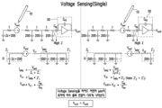
도 1은 종래의 터치 입력 장치 내의 플렉서블 디스플레이 패널 상에서 스타일러스 펜(10)의 위치에 따라 CVA(Capacitance to Voltage Amplifier)의 출력전압(Vout)이 달라지는 것을 설명하기 위한 개략적인 도면이다.Figure 1 is a schematic diagram to explain that the output voltage (Vout) of a CVA (Capacitance to Voltage Amplifier) varies depending on the position of the
도 1을 참조하면, 플렉서블 디스플레이 패널 상의 펜(10)의 위치에 따라 CVA의 출력이 다르게 나오는 원인은, 감지 라인 상에서 펜(10)을 중심으로 한 양쪽의 임피던스(impedance) 비율이 달라짐에 있다.Referring to FIG. 1, the reason why the output of the CVA varies depending on the position of the
종래의 플렉서블 디스플레이 패널의 장축 기준으로, 메탈 메쉬(Metal Mesh) 터치 센서의 저항(R)은 대략 1.2k (ohm)이고, 커패시터(C)는 대략 250pF이다.Based on the long axis of a conventional flexible display panel, the resistance (R) of the metal mesh touch sensor is approximately 1.2k (ohm), and the capacitor (C) is approximately 250pF.
10개의 분산 모델(distributed model) 기준으로, 구동주파수 300kHz에서는 커패시터(capacitor)의 임피던스(impedance)가 저항보다 대략 200배(120 (ohm) vs. 1/(2π*300k*25pF) = 21k (ohm)) 더 크다. 따라서, 커패시터(capacitor)가 주요한 원인이다.Based on 10 distributed models, at a driving frequency of 300kHz, the impedance of the capacitor is approximately 200 times that of the resistor (120 (ohm) vs. 1/(2π*300k*25pF) = 21k (ohm) )) It's bigger. Therefore, capacitors are the main cause.
도 2는 도 1에서 펜(10)의 위치에 따라 CVA의 출력전압(Vout1, Vout2)이 다르다는 것을 전류 센싱(current sensing)을 통해 설명하기 위한 도면이고, 도 3은 도 1에서 펜(10)의 위치에 따라 CVA의 출력전압(Vout1, Vout2)이 다르다는 것을 전압 센싱(voltage sensing)을 통해 설명하기 위한 도면이다.FIG. 2 is a diagram for explaining through current sensing that the output voltages (Vout1, Vout2) of the CVA are different depending on the position of the
도 2 및 도 3을 참조하면, 감지 라인 상에서 펜(10)의 위치에 따라, CVA의 출력전압이 다르다. 즉, 감지 회로부(50) 측에 펜(10)이 가까울수록 CVA의 출력전압이 크고, 감지 회로부(50) 측으로부터 멀어질수록 CVA의 출력전압이 작아진다.Referring to Figures 2 and 3, the output voltage of the CVA varies depending on the position of the
본 발명이 해결하고자 하는 과제는, 터치 위치를 검출하고, 스타일러스 펜을 구동시키며, 스타일러스 펜의 위치를 검출할 수 있는 다기능의 터치 입력 장치를 제공한다.The problem to be solved by the present invention is to provide a multi-functional touch input device that can detect a touch position, drive a stylus pen, and detect the position of the stylus pen.
또한, 터치 위치 검출 시에 노이즈를 제거하여 터치 위치 센싱 감도를 향상시킬 수 있는 터치 입력 장치를 제공한다.Additionally, a touch input device that can improve touch position sensing sensitivity by removing noise when detecting a touch position is provided.
본 발명의 일 실시 형태에 따른 터치 입력 장치는, 센서부 및 상기 센서부와 전기적으로 연결된 제어부를 포함하고, 상기 센서부는 동일층에 함께 배치된 제1 내지 제4 패턴을 포함하고, 상기 제1 패턴은 서로 수직한 제1 방향과 제2 방향을 따라 다수로 배열되고 내부에 상기 제2 패턴이 배치된 개구부를 갖고, 상기 제3 패턴은 상기 제1 패턴을 기준으로 양 측에 각각 적어도 하나 배치되고 내부에 상기 제4 패턴이 배치된 개구부를 갖고, 상기 다수의 제1 패턴은 상기 제1 방향을 따라 교번하며 배치된 제1 홀수 패턴과 제1 짝수 패턴을 포함하고, 상기 제1 방향을 따라 배열된 제1 홀수 패턴들은 서로 전기적으로 연결되고, 상기 제1 방향을 따라 배열된 제1 짝수 패턴들은 서로 전기적으로 연결되고, 상기 다수의 제2 패턴 중 상기 제1 방향을 따라 배열된 제2 패턴들은 서로 전기적으로 연결되고, 상기 제1 방향을 따라 배열된 제2 패턴들 중 타 측 가장자리에 배치된 제2 패턴은 상기 제2 방향을 따라 배열된 제2 패턴들과 전기적으로 연결되고, 상기 다수의 제3 패턴 중 상기 제2 방향을 따라 배열된 제3 패턴들은 서로 전기적으로 연결되고, 상기 다수의 제4 패턴 중 상기 제2 방향을 따라 배열된 제4 패턴들은 서로 전기적으로 연결되고, 상기 제2 방향을 따라 배열된 제4 패턴들 중 타 측 가장자리에 배치된 제4 패턴은 상기 제1 방향을 따라 배열된 제4 패턴들과 전기적으로 연결된다.A touch input device according to an embodiment of the present invention includes a sensor unit and a control unit electrically connected to the sensor unit, wherein the sensor unit includes first to fourth patterns arranged together on the same layer, and the first A plurality of patterns are arranged in a first direction and a second direction perpendicular to each other and have an opening in which the second pattern is disposed, and at least one third pattern is disposed on both sides of the first pattern. and has an opening inside which the fourth pattern is disposed, wherein the plurality of first patterns include first odd-numbered patterns and first even-numbered patterns alternately arranged along the first direction, and Arranged first odd patterns are electrically connected to each other, first even number patterns arranged along the first direction are electrically connected to each other, and among the plurality of second patterns, a second pattern is arranged along the first direction. are electrically connected to each other, and a second pattern disposed on the other edge of the second patterns arranged along the first direction is electrically connected to the second patterns arranged along the second direction, and the plurality of Among the third patterns, third patterns arranged along the second direction are electrically connected to each other, and among the plurality of fourth patterns, fourth patterns arranged along the second direction are electrically connected to each other, and the fourth patterns are electrically connected to each other. Among the fourth patterns arranged along the second direction, a fourth pattern arranged at the other edge is electrically connected to the fourth patterns arranged along the first direction.
본 발명의 다른 실시 형태에 따른 터치 입력 장치는, 센서부 및 상기 센서부와 전기적으로 연결된 제어부를 포함하고, 상기 센서부는 동일층에 함께 배치된 제1 내지 제4 패턴을 포함하고, 상기 제1 패턴은 서로 수직한 제1 방향과 제2 방향을 따라 다수로 배열되고 내부에 상기 제2 패턴이 배치된 개구부를 갖고, 상기 제2 패턴은 상기 제3 패턴이 배치된 개구부를 갖고, 상기 제3 패턴은 상기 제4 패턴이 배치된 개구부를 갖고, 상기 다수의 제1 패턴은 상기 제1 방향을 따라 교번하며 배치된 제1 홀수 패턴과 제1 짝수 패턴을 포함하고, 상기 제1 방향을 따라 배열된 제1 홀수 패턴들은 서로 전기적으로 연결되고, 상기 제1 방향을 따라 배열된 제1 짝수 패턴들은 서로 전기적으로 연결되고, 상기 다수의 제2 패턴 중 상기 제1 방향을 따라 배열된 제2 패턴들은 서로 전기적으로 연결되고, 상기 제1 방향을 따라 배열된 제2 패턴들 중 타 측 가장자리에 배치된 제2 패턴은 상기 제2 방향을 따라 배열된 제2 패턴들과 전기적으로 연결되고, 상기 다수의 제3 패턴 중 상기 제2 방향을 따라 배열된 제3 패턴들은 서로 전기적으로 연결되고, 상기 다수의 제4 패턴 중 상기 제2 방향을 따라 배열된 제4 패턴들은 서로 전기적으로 연결되고, 상기 제2 방향을 따라 배열된 제4 패턴들 중 타 측 가장자리에 배치된 제4 패턴은 상기 제1 방향을 따라 배열된 제4 패턴들과 전기적으로 연결된다.A touch input device according to another embodiment of the present invention includes a sensor unit and a control unit electrically connected to the sensor unit, wherein the sensor unit includes first to fourth patterns arranged together on the same layer, and the first A plurality of patterns are arranged along first and second directions perpendicular to each other and have openings in which the second pattern is disposed, the second pattern has openings in which the third pattern is disposed, and the third pattern The pattern has an opening where the fourth pattern is disposed, and the plurality of first patterns include first odd patterns and first even patterns arranged alternately along the first direction, and are arranged along the first direction. The first odd-numbered patterns are electrically connected to each other, the first even-numbered patterns arranged along the first direction are electrically connected to each other, and among the plurality of second patterns, the second patterns arranged along the first direction are are electrically connected to each other, and a second pattern disposed on the other edge of the second patterns arranged along the first direction is electrically connected to the second patterns arranged along the second direction, and the plurality of Among the third patterns, third patterns arranged along the second direction are electrically connected to each other, and among the plurality of fourth patterns, fourth patterns arranged along the second direction are electrically connected to each other, and the second Among the fourth patterns arranged along the direction, a fourth pattern arranged at the other edge is electrically connected to the fourth patterns arranged along the first direction.
본 발명의 또 다른 실시 형태에 따른 터치 입력 장치는, 센서부 및 상기 센서부와 전기적으로 연결된 제어부를 포함하고, 상기 센서부는 동일층에 함께 배치된 제1 내지 제4 패턴을 포함하고, 상기 제1 패턴은 서로 수직한 제1 방향과 제2 방향을 따라 다수로 배열되고 내부에 상기 제2 패턴이 배치된 개구부를 갖고, 상기 제3 패턴은 상기 제2 방향을 따라 연장된 형상을 갖고, 상기 제2 방향을 따라 배열된 제1 패턴들을 둘러싸도록 배치되고, 내부에 상기 제4 패턴이 배치되는 개구부를 갖고, 상기 다수의 제1 패턴은 상기 제1 방향을 따라 교번하며 배치된 제1 홀수 패턴과 제1 짝수 패턴을 포함하고, 상기 제1 방향을 따라 배열된 제1 홀수 패턴들은 서로 전기적으로 연결되고, 상기 제1 방향을 따라 배열된 제1 짝수 패턴들은 서로 전기적으로 연결되고, 상기 다수의 제2 패턴 중 상기 제1 방향을 따라 배열된 제2 패턴들은 서로 전기적으로 연결되고, 상기 제1 방향을 따라 배열된 제2 패턴들 중 타 측 가장자리에 배치된 제2 패턴은 상기 제2 방향을 따라 배열된 제2 패턴들과 전기적으로 연결되고, 상기 다수의 제4 패턴의 타 단들은 서로 전기적으로 연결된다.A touch input device according to another embodiment of the present invention includes a sensor unit and a control unit electrically connected to the sensor unit, wherein the sensor unit includes first to fourth patterns arranged together on the same layer, and the first to fourth patterns are arranged together on the same layer. One pattern is arranged in multiple numbers along a first and second direction perpendicular to each other and has an opening in which the second pattern is disposed, and the third pattern has a shape extending along the second direction, It is arranged to surround first patterns arranged along a second direction, has an opening in which the fourth pattern is arranged, and the plurality of first patterns are arranged alternately along the first direction. and a first even-numbered pattern, wherein first odd-numbered patterns arranged along the first direction are electrically connected to each other, first even-numbered patterns arranged along the first direction are electrically connected to each other, and the plurality of Among the second patterns, second patterns arranged along the first direction are electrically connected to each other, and among the second patterns arranged along the first direction, a second pattern disposed on the other edge moves in the second direction. It is electrically connected to the second patterns arranged along, and other ends of the plurality of fourth patterns are electrically connected to each other.
본 발명의 또 다른 실시 형태에 다른 터치 입력 장치는, 센서부 및 상기 센서부와 전기적으로 연결된 제어부를 포함하고, 상기 센서부는 제1 층에 함께 배치된 제1 내지 제2 패턴, 및 상기 제1 층과 이격된 제2 층에 함께 배치된 제3 및 제4 패턴을 포함하고, 상기 제1 패턴은 서로 수직한 제1 방향과 제2 방향을 따라 다수로 배열되고 내부에 상기 제2 패턴이 배치된 개구부를 갖고, 상기 제3 패턴은 상기 제2 방향을 따라 연장된 형상을 갖고, 내부에 상기 제4 패턴이 배치된 개구부를 갖고, 상기 다수의 제1 패턴은 상기 제1 방향을 따라 교번하며 배치된 제1 홀수 패턴과 제1 짝수 패턴을 포함하고, 상기 제1 방향을 따라 배열된 제1 홀수 패턴들은 서로 전기적으로 연결되고, 상기 제1 방향을 따라 배열된 제1 짝수 패턴들은 서로 전기적으로 연결되고, 상기 다수의 제2 패턴 중 상기 제1 방향을 따라 배열된 제2 패턴들은 서로 전기적으로 연결되고, 상기 제1 방향을 따라 배열된 제2 패턴들 중 타 측 가장자리에 배치된 제2 패턴은 상기 제2 방향을 따라 배열된 제2 패턴들과 전기적으로 연결되고, 상기 다수의 제4 패턴의 타 단들은 서로 전기적으로 연결된다.A touch input device according to another embodiment of the present invention includes a sensor unit and a control unit electrically connected to the sensor unit, wherein the sensor unit includes first and second patterns arranged together on a first layer, and the first It includes third and fourth patterns arranged together on a second layer spaced apart from the layer, wherein the first patterns are arranged in multiple numbers along a first and second direction perpendicular to each other, and the second pattern is disposed therein. The third pattern has a shape extending along the second direction, has an opening in which the fourth pattern is disposed, and the plurality of first patterns alternate along the first direction. It includes arranged first odd patterns and first even patterns, wherein the first odd patterns arranged along the first direction are electrically connected to each other, and the first even patterns arranged along the first direction are electrically connected to each other. connected, second patterns arranged along the first direction among the plurality of second patterns are electrically connected to each other, and a second pattern disposed on the other edge among the second patterns arranged along the first direction. is electrically connected to second patterns arranged along the second direction, and other ends of the plurality of fourth patterns are electrically connected to each other.
본 발명의 실시 형태에 따른 터치 입력 장치를 사용하면, 터치 위치를 검출하고, 스타일러스 펜을 구동시키며, 스타일러스 펜의 위치를 검출할 수 있는 이점이 있다.Using the touch input device according to the embodiment of the present invention has the advantage of detecting the touch position, driving the stylus pen, and detecting the position of the stylus pen.
또한, 또한, 터치 위치 검출 시에 노이즈를 제거하여 터치 위치 센싱 감도를 향상시킬 수 있는 이점이 있다.Additionally, there is an advantage in that touch position sensing sensitivity can be improved by removing noise when detecting the touch position.
도 1은 종래의 터치 입력 장치 내의 플렉서블 디스플레이 패널 상에서 스타일러스 펜(10)의 위치에 따라 CVA(Capacitance to Voltage Amplifier)의 출력전압(Vout)이 달라지는 것을 설명하기 위한 개략적인 도면이다.
도 2는 도 1에서 펜(10)의 위치에 따라 CVA의 출력전압(Vout1, Vout2)이 다르다는 것을 전류 센싱(current sensing)을 통해 설명하기 위한 도면이다.
도 3은 도 1에서 펜(10)의 위치에 따라 CVA의 출력전압(Vout1, Vout2)이 다르다는 것을 전압 센싱(voltage sensing)을 통해 설명하기 위한 도면이다.
도 4는 본 발명의 제1 실시 형태에 따른 터치 입력 장치의 센서부(100)의 개략적인 구성도이다.
도 5는 도 4에 도시된 센서부(100)의 일 변형 예에 따른 센서부(100')이다.
도 6은 도 4에 도시된 본 발명의 제1 실시 형태에 따른 터치 입력 장치의 센서부(100)의 변형 예에 따른 센서부(100'')로서, 표 1의 No. 13을 설명하기 위한 도면이다.
도 7은 도 4에 도시된 센서부(100)의 변형 예에 따른 센서부(100''')의 개략적인 구성도이다.
도 8은 본 발명의 제2 실시 형태에 따른 터치 입력 장치를 설명하기 위한 도면이다.
도 9 내지 도 11은 도 8에 도시된 센서부(100a)를 위 <표 1>의 No.1으로 이용한 것을 설명하기 위한 도면들이다.
도 12는 본 발명의 제3 실시 형태에 따른 터치 입력 장치에 포함된 센서부(100b)를 설명하기 위한 도면이다.
도 13은 도 12에 도시된 센서부(100b)의 변형 예를 설명하기 위한 도면이다.
도 14는 본 발명의 제3 실시 형태에 따른 터치 입력 장치에 포함된 센서부(100c)를 설명하기 위한 도면이다.
도 15는 본 발명의 제4 실시 형태에 따른 터치 입력 장치에 포함된 센서부(100d)를 설명하기 위한 도면이다.
도 16은 도 15에 도시된 센서부(100d)의 변형 예를 설명하기 위한 도면이다.Figure 1 is a schematic diagram to explain that the output voltage (Vout) of a CVA (Capacitance to Voltage Amplifier) varies depending on the position of the
FIG. 2 is a diagram to explain through current sensing that the output voltages (Vout1 and Vout2) of the CVA are different depending on the position of the
FIG. 3 is a diagram to explain through voltage sensing that the output voltages (Vout1, Vout2) of the CVA are different depending on the position of the
Figure 4 is a schematic configuration diagram of the
FIG. 5 shows a sensor unit 100' according to a modified example of the
FIG. 6 shows a sensor unit 100'' according to a modified example of the
FIG. 7 is a schematic configuration diagram of the sensor unit 100''' according to a modified example of the
Figure 8 is a diagram for explaining a touch input device according to a second embodiment of the present invention.
FIGS. 9 to 11 are diagrams for explaining the use of the
FIG. 12 is a diagram for explaining the
FIG. 13 is a diagram for explaining a modified example of the
FIG. 14 is a diagram for explaining the
FIG. 15 is a diagram for explaining the
FIG. 16 is a diagram for explaining a modified example of the
후술하는 본 발명에 대한 상세한 설명은, 본 발명이 실시될 수 있는 특정 실시 형태를 예시로서 도시하는 첨부 도면을 참조한다. 이들 실시 형태는 당업자가 본 발명을 실시할 수 있기에 충분하도록 상세히 설명된다. 본 발명의 다양한 실시 형태는 서로 다르지만 상호 배타적일 필요는 없음이 이해되어야 한다. 예를 들어, 여기에 기재되어 있는 특정 형상, 구조 및 특성은 일 실시 형태에 관련하여 본 발명의 정신 및 범위를 벗어나지 않으면서 다른 실시 형태로 구현될 수 있다. 또한, 각각의 개시된 실시 형태 내의 개별 구성요소의 위치 또는 배치는 본 발명의 정신 및 범위를 벗어나지 않으면서 변경될 수 있음이 이해되어야 한다. 따라서, 후술하는 상세한 설명은 한정적인 의미로서 취하려는 것이 아니며, 본 발명의 범위는, 적절하게 설명된다면, 그 청구항들이 주장하는 것과 균등한 모든 범위와 더불어 첨부된 청구항에 의해서만 한정된다. 도면에서 유사한 참조부호는 여러 측면에 걸쳐서 동일하거나 유사한 기능을 지칭한다.The detailed description of the present invention described below refers to the accompanying drawings, which show by way of example specific embodiments in which the present invention may be practiced. These embodiments are described in sufficient detail to enable any person skilled in the art to practice the invention. It should be understood that the various embodiments of the present invention are different from one another but are not necessarily mutually exclusive. For example, specific shapes, structures and characteristics described herein may be implemented in one embodiment or another without departing from the spirit and scope of the invention. Additionally, it should be understood that the location or arrangement of individual components within each disclosed embodiment may be changed without departing from the spirit and scope of the invention. Accordingly, the detailed description that follows is not intended to be taken in a limiting sense, and the scope of the invention is limited only by the appended claims, together with all equivalents to what those claims assert, if properly described. Similar reference numbers in the drawings refer to identical or similar functions across various aspects.
본 문서의 다양한 실시 형태들에 따른 터치 입력 장치는, 전자 디바이스로서, 통상의 스마트폰과 같은 터치 입력 장치일 수도 있고, 통상의 스마트폰의 화면보다 상대적으로 더 큰 직사각형의 화면을 가지며, 대각 길이가 대략 10인치 이상 13인치 사이의 터치 입력 장치일 수 있다. 예를 들면, 폴더식 스마트폰(smartphone), 태블릿 PC(tablet personal computer), 차량용 디스플레이 장치, 전자책 리더기(e-book reader), 랩탑 PC(laptop personal computer), 넷북 컴퓨터(netbook computer) 중 적어도 하나를 포함할 수 있다. The touch input device according to various embodiments of this document is an electronic device, and may be a touch input device such as a typical smartphone, and has a rectangular screen that is relatively larger than the screen of a typical smartphone, and has a diagonal length. It may be a touch input device approximately between 10 inches and 13 inches. For example, at least one of a folding smartphone, a tablet personal computer, a vehicle display device, an e-book reader, a laptop personal computer, and a netbook computer. It can contain one.
또한, 본 발명의 다양한 실시 형태들에 따른 터치 입력 장치는, 화면 상에 위치한 손가락과 같은 객체의 위치를 검출할 수 있을 뿐만 아니라, 스타일러스 펜을 구동하기 위한 구동 신호를 출력하고, 스타일러스 펜으로부터 방출되는 신호를 감지하여 화면 상에 위치한 스타일러스 펜의 위치를 검출할 수 있다.In addition, the touch input device according to various embodiments of the present invention can not only detect the position of an object such as a finger located on the screen, but also output a drive signal for driving the stylus pen and emit a signal from the stylus pen. By detecting the signal, the position of the stylus pen located on the screen can be detected.
이하에서는 여러 실시 형태들을 첨부된 도면들을 참조하여 상세히 설명한다.Hereinafter, various embodiments will be described in detail with reference to the attached drawings.
도 4는 본 발명의 제1 실시 형태에 따른 터치 입력 장치의 센서부(100)의 개략적인 구성도이고, 도 5는 도 4에 도시된 센서부(100)의 일 변형 예에 따른 센서부(100')이다.FIG. 4 is a schematic configuration diagram of the
본 발명의 제1 실시 형태에 따른 터치 입력 장치는 포트레이트(portrait) 타입의 터치 입력 장치일 수 있다. 이러한 포트레이트 타입의 터치 입력 장치는 폭이 높이보다 작고, 센서부(100)를 제어하는 제어부(미도시)가 센서부(100)의 아래에 배치된다. 예를 들어, 스마트폰의 형상에 대응된다. The touch input device according to the first embodiment of the present invention may be a portrait type touch input device. This portrait-type touch input device has a width that is smaller than the height, and a control unit (not shown) that controls the
센서부(100)는 화면 상에 위치한 손가락과 같은 객체의 위치를 검출할 수 있을 뿐만 아니라, 화면 상에 위치한 스타일러스 펜을 구동시킬 수 있으며, 스타일러스 펜으로부터 방출되는 신호를 감지하여 화면 상에 위치한 스타일러스 펜의 위치를 검출할 수 있다.The
센서부(100)는 다수의 패턴(또는 다수의 전극)을 포함한다. The
센서부(100)는 다수의 제1 내지 제4 패턴(101, 102, 103, 104)을 포함할 수 있다. The
제1 패턴(101)은 임의의 제1 방향(y)을 따라 연장된 형상을 갖는다. 제1 방향은 터치 입력 장치의 화면의 장축 방향일 수 있다. 제1 패턴(101)은, ATX(Active TX)로도 명명될 수 있다.The
제1 패턴(101)에는 두 개의 전도성 패턴이 연결될 수 있다. 하나의 전도성 패턴은 제1 터치 센싱 수신 채널(FRX_E)의 전기적 경로가 되고, 다른 하나의 전도성 패턴은 제2 터치 센싱 수신 채널(FRX_O)의 전기적 경로가 될 수 있다. 하나의 전도성 패턴은 제1 패턴(101)에 포함된 제1 홀수 패턴들과 전기적으로 연결되고, 다른 하나의 전도성 패턴은 제1 패턴(101)에 포함된 제1 짝수 패턴들과 전기적으로 연결된다. 제1 홀수 패턴들과 제1 짝수 패턴들에 대해서는 도 8 내지 도 16에서 설명하도록 한다. 한편, 상기 두 개의 전도성 패턴은 스타일러스 센싱 채널(SRX)의 전기적 경로가 될 수도 있다.Two conductive patterns may be connected to the
제2 패턴(102)은 제1 방향(y)을 따라 연장된 형상을 가지며, 제1 패턴(101)에 인접하여 배치되고, 제1 패턴(101)과 소정 간격 떨어져 배치된다. 제2 패턴(102)은, DTX(Dummy TX)로도 명명될 수 있다.The
제3 패턴(103)은 제1 방향과 다른 제2 방향(x)을 따라 연장된 형상을 갖는다. 제2 방향(x)은 제1 방향(y)과 수직한 방향일 수 있으며, 터치 입력 장치의 화면의 단축 방향일 수 있다. 제3 패턴(103)은, ARX(Active RX)로도 명명될 수 있다.The
제4 패턴(104)은 제2 방향(x)을 따라 연장된 형상을 가지며, 제3 패턴(103)에 인접하여 배치되고, 제3 패턴(103)과 소정 간격 떨어져 배치된다. 제4 패턴(104)은, DRX(dummy RX)로도 명명될 수 있다. The
제3 및 제4 패턴(103, 104)은 제1 및 제2 패턴(101, 102) 상에 배치되고, 제1 및 제2 패턴(101, 102)와 소정 간격 떨어져 배치된다. 한편, 별도의 도면으로 도시하지 않았지만, 제1 내지 제4 패턴이 동일층에 배치될 수도 있다. The third and
다수의 제1 패턴(101)들은 제2 방향(x)을 따라 배열되고, 다수의 제2 패턴(102)들도 제2 방향(x)을 따라 배열된다. 다수의 제3 패턴(103)들은 제1 방향(y)을 따라 배열되고, 다수의 제4 패턴(104)들도 제1 방향(y)을 따라 배열된다. The plurality of
제1 패턴(101)이 제1 방향(y)을 따라 연장되고 제3 패턴(103)이 제2 방향(x)을 따라 연장되고, 제1 방향(y)이 제2 방향(x)보다 더 길기 때문에, 다수의 제1 패턴(101)들의 개수는 다수의 제3 패턴(103)들의 개수보다 적다. 따라서, 다수의 제1 패턴(101)들의 채널(Channel) 수는 다수의 제3 패턴(103)들의 채널 수보다 적다.The
여기서, 다수의 제1 패턴(101)들의 개수와 다수의 제3 패턴(103)들의 개수는 터치 입력 장치의 화면의 크기에 따라 증가될 수도 있고, 감소할 수도 있다. Here, the number of
다수의 제2 패턴(102)들은 다수의 제1 패턴(101)들과 동일한 개수로 구성될 수 있다. 다수의 제2 패턴(102)들 각각의 타 단들은 전도성 패턴(102m)을 통해 서로 전기적으로 연결된다. 여기서, 전도성 패턴(102m)은 메탈 메쉬(Metal Mesh) 또는 실버 트레이스(Silver Trace)일 수 있다.The number of
다수의 제2 패턴(102)의 각각의 일 단들이 개별적으로 하나의 전도성 패턴에 연결될 수 있다. 여기서, 다수의 제2 패턴(102)의 각각의 일 단들이 개별적으로 연결된 전도성 패턴은 하나의 스타일러스 구동 채널(STX)의 전기적 경로가 될 수 있다.Each end of the plurality of
한편, 도 5에 도시된 바와 같이, 다수의 제2 패턴(102)들 중 서로 인접한 둘 이상의 제2 패턴(102)의 일 단들이 전도성 패턴을 통해 서로 전기적으로 연결될 수도 있다. 이러한 구성으로 인해, 다수의 제2 패턴(102)들의 채널 수가 다수의 제1 패턴(101)들의 채널 수의 절반으로 줄어들 수 있다. Meanwhile, as shown in FIG. 5, ends of two or more
다시, 도 4를 참조하면, 다수의 제3 패턴(103)들이 제1 방향(y)을 따라 배열되므로 다수의 제3 패턴(103)들의 개수는 다수의 제1 패턴(101)들의 개수보다 많다. 따라서, 다수의 제3 패턴(103)들의 채널 수는 다수의 제1 패턴(101)들의 채널 수보다 많다. Again, referring to FIG. 4, since the plurality of
다수의 제3 패턴(103)들 각각의 일 단에는 하나의 전도성 패턴이 연결될 수 있다. 다수의 제3 패턴(103)들 각각의 일 단에 연결된 전도성 패턴은 터치 센싱 구동 채널(FTX)의 전기적 경로 또는/및 스타일러스 센싱 채널(SRX)의 전기적 경로가 될 수 있다. 여기서, 터치 입력 장치의 좌우 베젤의 폭을 고려하여, 다수의 제3 패턴(103)들 중 절반은 우측단에 전도성 패턴이 연결되고, 나머지 절반은 좌측단에 전도성 패턴이 연결될 수 있다.One conductive pattern may be connected to one end of each of the plurality of
다수의 제4 패턴(104)들은 다수의 제3 패턴(103)들과 동일한 개수로 구성될 수 있다. 다수의 제4 패턴(104)들 각각의 타 단들은 전도성 패턴(104ml, 104mr)을 통해 서로 전기적으로 연결된다. 여기서, 전도성 패턴(104ml, 104mr)은 다수의 제4 패턴(104)들 중 절반의 제4 패턴(104)들의 좌측단을 연결하는 좌측 전도성 패턴(104ml)과 나머지 절만의 제4 패턴들의 우측단을 연결하는 우측 전도성 패턴(104mr)을 포함할 수 있다. 좌측 전도성 패턴(104ml)과 우측 전도성 패턴(104mr)은 다수의 제3 패턴(103)들과 연결된 전도성 패턴들과 서로 겹치거나 교차되지 않도록 배열될 수 있다.The number of
이러한 도 4에 도시된 터치 입력 장치의 센서부(100)에 있어서, 다수의 제1 패턴(101)들과 다수의 제3 패턴(103)들은 기본적으로 손가락과 같은 객체의 터치를 센싱한다. 이를 위해, 다수의 제1 패턴(101)들은 터치 구동 신호가 인가되는 터치 구동 전극으로 동작하고, 다수의 제3 패턴(103)들은 터치 감지 신호가 수신되는 터치 감지 전극(또는 터치 수신 전극)으로 동작할 수 있다. 물론, 반대로도 동작할 수 있다. In the
도 4에 도시된 터치 입력 장치의 센서부(100)가 스타일러스 펜을 구동(driving)하고 센싱(sensing)하기 위해, 다수의 제1 내지 제4 패턴들(101, 102, 103, 104)이 다양한 조합으로서 이용될 수 있다. 다양한 조합은 아래 <표 1>과 같다. 아래 <표 1>에서, '1'은 다수의 제1 패턴(101)을, '2'는 다수의 제2 패턴(102)을, '3은 다수의 제3 패턴(103)을, '4'는 다수의 제4 패턴(104)을 지칭한다. In order for the
위 <표 1>을 참조하면, 여러 조합들(No.1 내지 No.32)에 있어서, 다수의 제1 패턴(101)들과 다수의 제3 패턴(103)들은 손가락과 같은 객체의 터치를 센싱한다. 구체적으로, 다수의 제3 패턴(103)들은 터치 구동 전극으로서 동작하고, 다수의 제1 패턴(101)들은 터치 수신 전극으로서 동작한다.Referring to <Table 1> above, in various combinations (No. 1 to No. 32), a plurality of
다수의 제1 내지 제4 패턴(101, 102, 103, 104)들 중 하나 또는 둘은 스타일러스 펜을 구동시키기 위한 스타일러스 구동 전극으로 동작할 수 있다. 제1 내지 제4 패턴(101, 102, 103, 104) 중 하나 또는 둘의 패턴을 이용하여 스타일러스 펜을 구동시키기 위한 전류 루프를 형성할 수 있다. X축 구동은 다수의 제1 패턴(101)들과 다수의 제2 패턴(102)들 중 어느 하나를, Y축 구동은 다수의 제3 패턴(103)들과 다수의 제4 패턴(104)들 중 어느 하나일 수 있다. 스타일러스 펜의 구동은 X축 구동과 Y축 구동 중 어느 하나로도 가능하고, 둘 다로도 가능하다.One or two of the first to
다수의 제1 내지 제4 패턴(101, 102, 103, 104)들 중 둘은 스타일러스 펜으로부터 방출되는 스타일러스 펜 신호를 센싱하는 센싱 전극으로 동작할 수 있다. 스타일러스 펜 신호를 센싱하기 위해서는 X축 센싱과 Y축 센싱이 함께 필요하므로, 다수의 제1 내지 제4 패턴(101, 102, 103, 104)들 중 두 개의 패턴들을 이용한다. X축 센싱은 다수의 제1 패턴(101)들과 다수의 제2 패턴(102)들 중 어느 하나일 수 있고, Y축 센싱은 다수의 제3 패턴(103)들과 다수의 제4 패턴(104)들 중 어느 하나일 수 있다.Two of the first to
위 <표 1>에서, '업링크(uplink) 신호 크기'란, 스타일러스 펜을 구동시키기 위한 구동 신호의 크기를 의미한다. 동일한 스타일러스 펜 구동 신호를 다수의 제1 패턴(101)들과 다수의 제2 패턴(102)들에 각각 인가하여 스타일러스 펜으로 수신되는 신호의 크기를 비교해보면, 다수의 제2 패턴(102)들에 스타일러스 펜 구동 신호를 인가한 경우가 다수의 제1 패턴(101)들에 스타일러스 펜 구동 신호를 인가한 경우보다 업링크 신호가 상대적으로 더 크다.In <Table 1> above, 'uplink signal size' refers to the size of the driving signal for driving the stylus pen. When comparing the size of the signal received by the stylus pen by applying the same stylus pen driving signal to each of the plurality of
왜냐하면, 다수의 제2 패턴(102)들은 타 단들은 전기적으로 연결되어 있어 스타일러스 펜 구동 신호가 인가되는 둘 이상의 제2 패턴들을 적절히 선택하면 적어도 하나 이상의 전류 루프가 형성되어 있지만, 다수의 제1 패턴(101)들의 타 단들은 서로 전기적으로 연결되어 있지 않아 전류 루프가 형성되지 못하기 때문이다. 각 제1 패턴(101)으로 전류가 흐를 경우, 각 제1 패턴(101)의 RC가 차징되므로 각 제1 패턴(101)의 일 단에서 타 단으로 갈수록 전류가 잘 흐르지 못한다. 또한, 다수의 제1 패턴(101)들을 통해서 인가되는 스타일러스 펜 구동 신호는 커패시티브 커플링을 통해 전류 루프가 형성된 다수의 제2 패턴(101)들로 전달되는데, 이때 커패시티브 커플링에 의해 신호 감쇠가 생기기 때문이다.This is because the other ends of the plurality of
마찬가지로, 다수의 제4 패턴(104)들에 스타일러스 펜 구동 신호를 인가한 경우가 다수의 제3 패턴(103)들에 스타일러스 펜 구동 신호를 인가한 경우보다 업링크 신호가 상대적으로 더 크다.Similarly, when the stylus pen driving signal is applied to the plurality of
위 <표 1>에서, '다운링크(downlink) 신호 크기'란, 스타일러스 펜으로부터 수신되는 스타일러스 펜 신호의 크기를 의미한다. 동일한 스타일러스 펜 신호를 다수의 제1 패턴(101)들과 다수의 제2 패턴(102)들을 통해 각각 수신하여 신호의 크기를 비교해보면, 다수의 제2 패턴(102)들을 통해 스타일러스 펜 신호를 수신한 경우가 다수의 제1 패턴(101)들을 통해 스타일러스 펜 신호를 수신한 경우보다 다운링크 신호가 상대적으로 더 크다. 그 이유는, 다수의 제2 패턴(102)들은 타 단들은 전기적으로 연결되어 있어 전류 루프가 형성되어 있지만, 다수의 제1 패턴(101)들은 타 단들은 서로 전기적으로 연결되어 있지 않고, 특히, 커패시티브 커플링을 통해 전류 루프가 형성된 다수의 제2 패턴(101)들로부터 스타일러스 펜 신호가 다수의 제1 패턴(101)들로 전달되므로 이 때 다운링크 신호의 감쇠가 생기기 때문이다.In <Table 1> above, 'downlink signal size' refers to the size of the stylus pen signal received from the stylus pen. When comparing the size of the signal by receiving the same stylus pen signal through a plurality of
마찬가지로, 다수의 제4 패턴(104)들을 통해 스타일러스 펜 신호를 수신한 경우가 다수의 제3 패턴(103)들을 통해 스타일러스 펜 신호를 수신한 경우보다 다운링크 신호가 상대적으로 더 크다.Likewise, when a stylus pen signal is received through a plurality of
위 <표 1>에서, '스타일러스(stylus) 추가 채널'이란, 터치 센싱 이외에 스타일러스 펜을 위해 추가적인 채널을 구성해야 하느냐를 의미한다. 스타일러스 펜의 구동(driving)이나 센싱(sensing)을 위해서 다수의 제2 패턴(102)들 또는/및 다수의 제4 패턴(104)들을 이용하는 경우에는 추가 채널이 필요(<표 1>에서 '유'로 표시)하다. 반면, 스타일러스 펜의 구동이나 센싱을 터치 센싱을 위한 다수의 제1 패턴(101)들 또는/및 제3 패턴(103)들을 이용하는 경우에는 추가 채널이 불필요(<표 1>에서 '무'로 표시)하다.In <Table 1> above, 'stylus additional channel' means whether an additional channel must be configured for the stylus pen in addition to touch sensing. When using a plurality of
이하, 위 <표 1>의 여러 조합들(No.1 내지 No. 32) 중 몇 가지 예들을 이하에서 상세히 설명한다. 여기서, 설명하지 않은 조합들은 이하의 상세한 설명에 의해 당업자라면 충분히 이해할 수 있을 것이다.Hereinafter, some examples of the various combinations (No. 1 to No. 32) in <Table 1> above will be described in detail below. Combinations not described herein will be fully understood by those skilled in the art through the detailed description below.
No.1에 있어서, 다수의 제1 패턴(101)들은 객체의 터치 센싱을 위한 터치 수신 전극으로서 이용되면서 스타일러스 펜 신호를 감지하는 스타일러스 감지 전극으로서 이용된다. 다수의 제2 패턴(102)들은 스타일러스 펜을 구동시키기 위한 스타일러스 구동 전극으로서 이용된다. 다수의 제3 패턴(103)들은 객체의 터치 센싱을 위한 터치 구동 전극으로 이용되면서 스타일러스 펜 신호를 센싱하기 위한 스타일러스 감지 전극으로서 이용된다. 그리고, 다수의 제4 패턴(104)들은 전기적으로 플로팅된다. In No. 1, the plurality of
No.1의 경우, 다수의 제2 패턴(102)들을 스타일러스 구동 전극으로서 이용하므로, 업링크 신호의 크기가 상대적으로 크다. 다수의 제1 패턴(101)들과 다수의 제3 패턴(103)들을 스타일러스 감지 전극으로서 이용하므로 다운링크 신호의 크기가 상대적으로 작다. 그리고, 다수의 제2 패턴(102)들을 스타일러스 구동 전극으로서 별도로 이용하므로, 스타일러스 펜의 구동을 위한 별도의 추가 채널이 필요하지만, 스타일러스 펜의 센싱을 위한 추가 채널이 불필요하다.In the case of No. 1, since a plurality of
No.4에 있어서, 다수의 제1 패턴(101)들은 객체의 터치 센싱을 위한 터치 감지 전극으로서 이용된다. 다수의 제2 패턴(102)들은 스타일러스 펜을 구동시키기 위한 스타일러스 구동 전극으로서 이용되면서 스타일러스 펜 신호를 센싱하기 위한 스타일러스 감지 전극으로서 이용된다. 다수의 제3 패턴(103)들은 객체의 터치 센싱을 위한 터치 구동 전극으로 이용된다. 그리고, 다수의 제4 패턴(104)들은 스타일러스 펜 신호를 센싱하기 위한 스타일러스 감지 전극으로서 이용된다. In No. 4, the plurality of
No.4의 경우, 다수의 제2 패턴(102)들을 스타일러스 구동 전극으로서 이용하므로, 업링크 신호의 크기가 상대적으로 크다. 다수의 제2 패턴(102)들과 다수의 제4 패턴(104)들을 스타일러스 감지 전극으로서 이용하므로 다운링크 신호의 크기가 상대적으로 크다. 그리고, 다수의 제2 패턴(102)들을 스타일러스 구동 전극 및 스타일러스 감지 전극으로서 별도로 이용하고 다수의 제4 패턴(104)들을 스타일러스 감지 전극으로서 별도로 이용되므로, 스타일러스 펜의 구동과 센싱을 위한 별도의 추가 채널이 필요하다.In the case of No. 4, since a plurality of
No.8에 있어서, 다수의 제1 패턴(101)들은 객체의 터치 센싱을 위한 터치 감지 전극으로서 이용된다. 다수의 제2 패턴(102)들은 스타일러스 펜 신호를 센싱하기 위한 스타일러스 감지 전극으로서 이용된다. 다수의 제3 패턴(103)들은 객체의 터치 센싱을 위한 터치 구동 전극으로 이용된다. 그리고, 다수의 제4 패턴(104)들은 스타일러스 펜을 구동시키기 위한 스타일러스 구동 전극으로서 이용되면서 스타일러스 펜 신호를 센싱하기 위한 스타일러스 감지 전극으로서 이용된다. In No. 8, the plurality of
No.8의 경우, 다수의 제4 패턴(104)들을 스타일러스 구동 전극으로서 이용하므로, 업링크 신호의 크기가 상대적으로 크다. 다수의 제2 패턴(102)들과 다수의 제4 패턴(104)들을 스타일러스 감지 전극으로서 이용하므로 다운링크 신호의 크기가 상대적으로 크다. 그리고, 다수의 제2 패턴(102)들을 스타일러스 감지 전극으로서 별도로 이용하고 다수의 제4 패턴(104)들을 스타일러스 구동 전극 및 스타일러스 감지 전극으로서 별도로 이용하므로, 스타일러스 펜의 구동과 센싱을 위한 별도의 추가 채널이 필요하다.In the case of No. 8, since a plurality of
No.12에 있어서, 다수의 제1 패턴(101)들은 객체의 터치 센싱을 위한 터치 감지 전극으로서 이용된다. 다수의 제2 패턴(102)들은 스타일러스 펜을 구동시키기 위한 스타일러스 구동 전극으로 이용되면서 스타일러스 펜 신호를 센싱하기 위한 스타일러스 감지 전극으로서 이용된다. 다수의 제3 패턴(103)들은 객체의 터치 센싱을 위한 터치 구동 전극으로 이용된다. 그리고, 다수의 제4 패턴(104)들은 스타일러스 펜을 구동시키기 위한 스타일러스 구동 전극으로서 이용되면서 스타일러스 펜 신호를 센싱하기 위한 스타일러스 감지 전극으로서 이용된다. In No. 12, the plurality of
No.12의 경우, 다수의 제2 및 제4 패턴(102, 104)들을 스타일러스 구동 전극으로서 이용하므로, 업링크 신호의 크기가 상대적으로 크다. 다수의 제2 패턴(102)들과 다수의 제4 패턴(104)들을 스타일러스 감지 전극으로서 이용하므로 다운링크 신호의 크기가 상대적으로 크다. 그리고, 다수의 제2 패턴(102)들을 스타일러스 구동 전극 및 스타일러스 감지 전극으로서 별도로 이용하고 다수의 제4 패턴(104)들을 스타일러스 구동 전극 및 스타일러스 감지 전극으로서 별도로 이용하므로, 스타일러스 펜의 구동과 센싱을 위한 별도의 추가 채널이 필요하다.In the case of No. 12, since a plurality of second and
도 6은 도 4에 도시된 본 발명의 제1 실시 형태에 따른 터치 입력 장치의 센서부(100)의 변형 예에 따른 센서부(100'')로서, 표 1의 No. 13을 설명하기 위한 도면이다. FIG. 6 shows a sensor unit 100'' according to a modified example of the
도 6을 참조하면, No.13에 있어서, 다수의 제1 패턴(101)들은 객체의 터치 센싱을 위한 터치 감지 전극으로서 이용되고, 스타일러스 펜을 구동시키기 위한 스타일러스 구동 전극으로 이용되며, 스타일러스 펜 신호를 센싱하기 위한 스타일러스 감지 전극으로서 이용된다. 다수의 제3 패턴(103)들은 객체의 터치 센싱을 위한 터치 구동 전극으로 이용되고 스타일러스 펜 신호를 센싱하기 위한 스타일러스 감지 전극으로서 이용된다. 그리고, 다수의 제2 및 제4 패턴(102, 104)들은 전기적으로 플로팅된다.Referring to FIG. 6, in No. 13, a plurality of
No.13의 경우, 다수의 제1 패턴(101)들을 스타일러스 구동 전극으로서 이용하므로, 업링크 신호의 크기가 상대적으로 작다. 다수의 제1 패턴(101)들과 다수의 제3 패턴(103)들을 스타일러스 감지 전극으로서 이용하므로 다운링크 신호의 크기가 상대적으로 작다. 그리고, 다수의 제1 패턴(102)들을 스타일러스 구동 전극 및 스타일러스 감지 전극으로서 이용하고 다수의 제3 패턴(103)들을 스타일러스 감지 전극으로서 이용하므로, 스타일러스 펜의 구동과 센싱을 위한 별도의 추가 채널이 불필요하다.In the case of No. 13, since a plurality of
No.17에 있어서, 다수의 제1 패턴(101)들은 객체의 터치 센싱을 위한 터치 감지 전극으로서 이용되고, 스타일러스 펜 신호를 센싱하기 위한 스타일러스 감지 전극으로서 이용된다. 다수의 제3 패턴(103)들은 객체의 터치 센싱을 위한 터치 구동 전극으로 이용되고, 스타일러스 펜을 구동시키기 위한 스타일러스 구동 전극으로 이용되며, 스타일러스 펜 신호를 센싱하기 위한 스타일러스 감지 전극으로서 이용된다. 그리고, 다수의 제2 및 제4 패턴(102, 104)들은 전기적으로 플로팅된다.In No. 17, the plurality of
No.17의 경우, 다수의 제3 패턴(103)들을 스타일러스 구동 전극으로서 이용하므로, 업링크 신호의 크기가 상대적으로 작다. 다수의 제1 패턴(101)들과 다수의 제3 패턴(103)들을 스타일러스 감지 전극으로서 이용하므로 다운링크 신호의 크기가 상대적으로 작다. 그리고, 다수의 제1 패턴(102)들을 스타일러스 감지 전극으로서 이용하고 다수의 제3 패턴(103)들을 스타일러스 구동 전극 및 스타일러스 감지 전극으로서 이용하므로, 스타일러스 펜의 구동과 센싱을 위한 별도의 추가 채널이 불필요하다.In the case of No. 17, since a plurality of
No.21에 있어서, 다수의 제1 패턴(101)들은 객체의 터치 센싱을 위한 터치 감지 전극으로서 이용되고, 스타일러스 펜을 구동시키기 위한 스타일러스 구동 전극으로 이용되며, 스타일러스 펜 신호를 센싱하기 위한 스타일러스 감지 전극으로서 이용된다. 다수의 제3 패턴(103)들은 객체의 터치 센싱을 위한 터치 구동 전극으로 이용되고, 스타일러스 펜을 구동시키기 위한 스타일러스 구동 전극으로 이용되며, 스타일러스 펜 신호를 센싱하기 위한 스타일러스 감지 전극으로서 이용된다. 그리고, 다수의 제2 및 제4 패턴(102, 104)들은 전기적으로 플로팅된다.In No. 21, the plurality of
No.21의 경우, 다수의 제1 및 3 패턴(101, 103)들을 스타일러스 구동 전극으로서 이용하므로, 업링크 신호의 크기가 상대적으로 작다. 다수의 제1 패턴(101)들과 다수의 제3 패턴(103)들을 스타일러스 감지 전극으로서 이용하므로 다운링크 신호의 크기가 상대적으로 작다. 그리고, 다수의 제1 패턴(102)들을 스타일러스 구동 전극 및 스타일러스 감지 전극으로서 이용하고 다수의 제3 패턴(103)들을 스타일러스 구동 전극 및 스타일러스 감지 전극으로서 이용하므로, 스타일러스 펜의 구동과 센싱을 위한 별도의 추가 채널이 불필요하다.In the case of No. 21, since a plurality of first and
위 <표 1>의 여러 조합들(No.1 내지 No.32) 중에서 Nos.1, 5, 9, 25, 29들은, '스타일러스 추가 채널'의 열에서 구동(driving)은 '유'이고, 센싱(sensing)은 '무'이다. 상기 Nos.1, 5, 9, 25, 29들은 스타일러스 펜을 센싱하는데 다수의 제1 및 제3 패턴(101, 103)들을 이용하고, 스타일러스 펜 구동하는데 다수의 제2 또는/및 제4 패턴(102, 104)들을 이용한다. 스타일러스 펜 구동 시, 다수의 제2 또는/및 제4 패턴(102, 104)들을 이용하더라도 스타일러스 펜을 공진시키기 위한 자기장 형성이 다소 어려울 수 있기 때문에, 도 5에 도시된 바와 같이 이웃하는 둘 이상의 제2 패턴들의 일 단들을 전기적으로 연결시킬 수 있다. 마찬가지로 이웃하는 둘 이상의 제4 패턴들의 일 단들을 전기적으로 연결시킬 수 있다. 이와같이 구성하면, 스타일러스 펜을 구동하기 위한 추가 채널을 줄일 수 있는 이점이 있다.Among the various combinations (No. 1 to No. 32) in <Table 1> above, for Nos. 1, 5, 9, 25, and 29, driving is 'Yes' in the column of 'Stylus additional channel', Sensing is ‘nothing.’ Nos. 1, 5, 9, 25, 29 use a plurality of first and third patterns (101, 103) to sense the stylus pen, and a plurality of second or/and fourth patterns (101, 103) to drive the stylus pen. 102, 104) are used. When driving the stylus pen, even if a plurality of second and/or
도 7은 도 4에 도시된 센서부(100)의 변형 예에 따른 센서부(100''')의 개략적인 구성도이다.FIG. 7 is a schematic configuration diagram of the sensor unit 100''' according to a modified example of the
도 7에 도시된 센서부(100''')는 도 6에 도시된 센서부(100'')와 비교하여, 다수의 제2 패턴(102)들을 전기적으로 연결하는 전도성 패턴(102mu, 102mb)과 다수의 제4 패턴(104)들을 전기적으로 연결하는 전도성 패턴(104ml, 104mr)에 있어서 차이가 있다. Compared to the sensor unit 100'' shown in FIG. 6, the sensor unit 100''' shown in FIG. 7 has conductive patterns 102mu and 102mb that electrically connect a plurality of
다수의 제2 패턴(102)들의 일 단들은 전도성 패턴(102mb)에 의해 서로 전기적으로 연결되고, 다수의 제2 패턴(102)들의 타 단들은 전도성 패턴(102mu)에 의해 서로 전기적으로 연결된다. 따라서, 다수의 제2 패턴(102)들은 온전한 전기적 루프를 형성할 수 있게 된다. One end of the plurality of
마찬가지로, 다수의 제4 패턴(104)들의 일 단들은 전도성 패턴(104mr)에 의해 서로 전기적으로 연결되고, 다수의 제4 패턴(104)들의 타 단들은 전도성 패턴(104ml)에 의해 서로 전기적으로 연결된다. 따라서, 다수의 제4 패턴(104)들은 온전한 전기적 루프를 형성할 수 있게 된다.Likewise, one end of the plurality of
다수의 제2 패턴(102)들과 다수의 제4 패턴(104)들이 온전한 전기적 루프를 형성하므로, 업링크 신호와 다운링크 신호의 감도가 도 6보다 더 향상될 수 있는 이점이 있다.Since the plurality of
도 8은 본 발명의 제2 실시 형태에 따른 터치 입력 장치를 설명하기 위한 도면이다.Figure 8 is a diagram for explaining a touch input device according to a second embodiment of the present invention.
도 8에 도시된 터치 입력 장치는 도 4에 도시된 터치 입력 장치가 구체화된 일 예일 수 있다.The touch input device shown in FIG. 8 may be an example of the touch input device shown in FIG. 4 being implemented.
도 8을 참조하면, 본 발명의 제2 실시 형태에 따른 터치 입력 장치는 센서부(100a)와 제어부(500)를 포함한다.Referring to FIG. 8, the touch input device according to the second embodiment of the present invention includes a
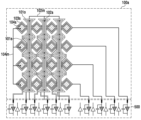
센서부(100a)는, 다수의 제1 내지 제4 패턴(101a, 102a, 103a, 104a)들을 포함한다. The
제1 패턴(101a)은 서로 수직한 제1 방향과 제2 방향을 따라 다수로 배열된다. 여기서, 제1 방향은 터치 입력 장치의 화면의 장축 방향일 수 있고, 제2 방향은 터치 입력 장치의 화면의 단축 방향일 수 있다.The
제1 패턴(101a)은 제1 홀수 패턴(101o)과 제1 짝수 패턴(101e)을 포함한다. 다수의 제1 패턴(101a)은 다수의 제1 홀수 패턴(101o)와 다수의 제1 짝수 패턴(101e)를 포함하고, 하나의 제1 홀수 패턴(101o)과 하나의 제1 짝수 패턴(101e)이 교번되면서 제1 방향을 따라 배열된다. The
제1 방향을 따라 배열된 다수의 제1 홀수 패턴(101o)은 다수의 전도성 패턴들에 의해 서로 전기적으로 연결되고, 제1 방향을 따라 배열된 다수의 제1 짝수 패턴(101e)도 다수의 전도성 패턴들에 의해 서로 전기적으로 연결된다. 여기서, 제2 방향을 따라 배열된 다수의 제1 홀수 패턴(101o)은 서로 전기적으로 연결되지 않는다. 또한, 제2 방향을 따라 배열된 다수의 제1 짝수 패턴(101e)도 서로 전기적으로 연결되지 않는다.The plurality of first odd patterns 101o arranged along the first direction are electrically connected to each other by a plurality of conductive patterns, and the plurality of first even
제1 홀수 패턴(101o)과 제1 짝수 패턴(101e) 각각은 역삼각 패턴부, 삼각 패턴부 및 역삼각 패턴부와 삼각 패턴부 사이를 연결하는 연결 패턴부를 포함할 수 있다. Each of the first odd pattern 101o and the first even
제1 홀수 패턴(101o)과 제1 짝수 패턴(101e) 각각은 내부에 적어도 하나의 제2 패턴(102a)이 배치되는 개구부를 가질 수 있다. 개구부의 형상은 제1 홀수 패턴(101o)과 제1 짝수 패턴(101e) 각각의 형상에 대응될 수 있다.Each of the first odd pattern 101o and the first even
하나의 제1 홀수 패턴(101o)은 하나의 제2 패턴(102a)를 둘러싸는 구조를 가져 서로 전기적으로 절연되고, 하나의 제1 짝수 패턴(101e)도 하나의 제2 패턴(102a)를 둘러싸는 구조를 가져 서로 전기적으로 절연된다.One first odd pattern 101o has a structure surrounding one
제1 방향을 따라 배열된 다수의 제1 패턴(101a)은, 도 4에 도시된 제1 패턴(101)과 같은 전기적 경로를 형성한다. 제1 방향을 따라 배열된 다수의 제1 패턴(101a)은, 2개의 입출력 채널(또는 단자)를 갖는다. 하나의 채널은 제1 방향을 따라 배열된 다수의 제1 홀수 패턴(101o)이 전도성 패턴들에 의해 전기적으로 연결된 채널이고, 나머지 하나의 채널은 제1 방향을 따라 배열된 다수의 제2 짝수 패턴(101e)이 전도성 패턴들에 의해 전기적으로 연결된 채널이다. 상기 2개의 채널은 제어부(500)와 각각 전기적으로 연결될 수 있다. The plurality of
제2 패턴(102a)은 다수의 제1 홀수 패턴(101o)과 다수의 제1 짝수 패턴(101e) 각각의 내부에 적어도 하나 이상 배치된다.At least one
제1 방향을 따라 배열된 다수의 제2 패턴(102a)은 다수의 전도성 패턴들에 의해 서로 전기적으로 연결된다. 제1 방향을 따라 서로 이웃한 2개의 제2 패턴들이 하나의 전도성 패턴에 의해 전기적으로 연결될 수 있다. 제1 방향을 따라 배열된 다수의 제2 패턴(102a)들 중 일 측 가장자리에 배치된 제2 패턴은 제어부(500)와 전기적으로 연결될 수 있고, 타 측 가장자리에 배치된 제2 패턴(102a)은 제2 방향을 따라 배열된 다수의 제2 패턴들과 전도성 패턴(102m)을 통해 전기적으로 연결된다. 이를 통해 도 4에 도시된 제2 패턴(102)의 전기적 연결 경로와 같게 구성될 수 있다.The plurality of
제1 패턴(101a)과 제2 패턴(102a)은 동일층에 배치될 수 있다. 메탈 메쉬(metal mesh)를 이용하여 제1 패턴(101a)과 제2 패턴(102a)을 동일층에 형성시킬 수 있다.The
제3 패턴(103a)은 제2 방향(또는 단축)을 따라 연장된 형상을 갖는다. The
제3 패턴(103a)은 다수의 다이아몬드 패턴부와, 다수의 다이아몬드 패턴부 중에서 서로 인접한 2개의 다이아몬드 패턴부 사이를 연결하는 연결 패턴부를 포함할 수 있다.The
제3 패턴(103a)은 내부에 제4 패턴(104a)이 배치되는 개구부를 가질 수 있다.The
제3 패턴(103a)은 제4 패턴(104a)를 둘러싸는 구조를 가질 수 있다. 제3 패턴(103a)은 제4 패턴(104a)로부터 소정 간격 떨어져 배치된다. 이를 통해 서로 전기적으로 절연된다.The
제4 패턴(104a)은 제3 패턴(103a)에 인접하여 배치되고, 제2 방향을 따라 연장된 형상을 가지며, 제3 패턴(103a) 내부에 배치된다.The
제4 패턴(104a)는 다수의 다이아몬드 패턴부와, 다수의 다이아몬드 패턴부 중에서 서로 인접한 2개의 다이아몬드 패턴부 사이를 연결하는 연결 패턴부를 포함할 수 있다.The
이러한 제3 패턴(103a)과 제4 패턴(104a)이 제1 방향을 따라 다수로 배치된다.A plurality of these
다수의 제3 패턴(103a)들의 일 단들은 제어부(500)와 전기적으로 연결되고, 타 단들은 전기적으로 오픈(open)될 수 있다.One end of the plurality of
다수의 제4 패턴(104a)들의 일 단들은 도 8에 도시된 바와 같이 전기적으로 오픈(open)될 수도 있고, 도 8과는 다르게 제어부(500)와 연결될 수도 있다. 다수의 제4 패턴(104a)들의 타 단들은 전도성 패턴(104m)을 통해 서로 전기적으로 연결된다. 여기서, 서로 전기적으로 연결된 타 단들은 접지될 수도 있다. 다수의 제4 패턴(104a)들의 타 단들이 서로 전기적으로 연결되면, 각 제4 패턴(104a) 별 커패시턴스가 더해지므로 전체 임피던스는 줄어들게 되고, 다수의 제4 패턴(104a)들의 타 단들이 접지된 것과 유사한 효과를 가질 수 있다.One end of the plurality of
제3 패턴(103a)과 제4 패턴(104a)은 동일층에 배치될 수 있다. 메탈 메쉬(metal mesh)를 이용하여 제3 패턴(103a)과 제4 패턴(104a)을 동일층에 형성시킬 수 있다. 여기서, 제1 패턴(101a)과 제2 패턴(102a)은 제1 층에 배치되고, 제3 패턴(103a)과 제4 패턴(104a)은 제1 층과 다른 제2 층에 배치될 수 있다.The
제어부(500)는 센서부(100a)와 전기적으로 연결되며, 센서부(100a)를 제어한다. 제어부(500)와 센서부(100a)의 연결은 전도성 패턴을 통해 서로 전기적으로 연결될 수 있다.The
제어부(500)는 구동 회로부와 감지 회로부를 다수로 포함할 수 있다. The
다수의 구동 회로부는 터치 구동을 위한 구동 회로부와 스타일러스 구동을 위한 구동 회로부를 포함할 수 있다. The plurality of driving circuit units may include a driving circuit unit for touch driving and a driving circuit unit for stylus driving.
다수의 감지 회로부는 터치 센싱을 위한 감지 회로부와 스타일러스 센싱을 위한 감지 회로부를 포함할 수 있다. 여기서, 다수의 감지 회로부 중 일부의 감지 회로부는 터치 센싱도 수행하고, 스타일러스 센싱도 함께 수행할 수 있다. The plurality of sensing circuits may include a sensing circuit for touch sensing and a sensing circuit for stylus sensing. Here, some of the plurality of sensing circuit units may perform touch sensing and stylus sensing.
제어부(500)는 센서부(100a)를 터치 구동/센싱 모드, 안테나 구동 모드 및 스타일러스 센싱 모드 중 어느 하나의 모드로 동작하도록 제어할 수 있다. The
제어부(500)는 각 모드에 따라 다수의 구동/감지 회로부를 센서부(100a)와 전기적으로 연결시킬 수 있다. 이를 위해, 제어부(500)는 다수의 구동/감지 회로부와 센서부(100a)를 전기적으로 연결시키기 위한 다수의 스위치를 포함할 수 있다.The
도 9 내지 도 11은 도 8에 도시된 센서부(100a)를 위 <표 1>의 No.1으로 이용한 것을 설명하기 위한 도면들이다.FIGS. 9 to 11 are diagrams for explaining the use of the
도 9는 도 8에 도시된 터치 입력 장치가 터치 구동/센싱 모드(또는 2D 센싱 모드)로 동작하는 경우를 도시한 도면이고, 도 10은 도 8에 도시된 터치 입력 장치가 안테나 구동 모드(또는 스타일러스 구동 모드, 또는 스타일러스 업링크 모드)로 동작하는 경우를 도시한 도면이며, 도 11은 도 8에 도시된 터치 입력 장치가 스타일러스 센싱 모드(또는 스타일러스 다운링크 모드)로 동작하는 경우를 도시한 도면이다.FIG. 9 is a diagram illustrating a case where the touch input device shown in FIG. 8 operates in a touch driving/sensing mode (or 2D sensing mode), and FIG. 10 shows a case where the touch input device shown in FIG. 8 operates in an antenna driving mode (or It is a diagram showing a case where the touch input device shown in FIG. 8 operates in stylus sensing mode (or stylus downlink mode), and FIG. 11 is a diagram showing a case where the touch input device shown in FIG. 8 operates in stylus sensing mode (or stylus downlink mode) am.
도 9를 참조하면, 터치 구동/센싱 모드 시, 제어부(500)는 터치 구동을 위한 구동 회로부를 센서부(100a)의 제3 패턴(103a)에 전기적으로 연결시킬 수 있다. 다수의 제3 패턴(103a) 각각에 하나의 구동 회로부가 전기적으로 연결될 수 있다. Referring to FIG. 9 , in the touch driving/sensing mode, the
제어부(500)는 터치 센싱을 위한 감지 회로부를 센서부(100a)의 다수의 제1 패턴(101a)에 전기적으로 연결시킬 수 있다. 여기서, 제1 방향을 따라 배열된 다수의 제1 패턴(101a)은 제1 홀수 패턴(101o)들과 제2 짝수 패턴(101e)들을 갖는데, 제어부(500)는 제1 방향을 따라 배열된 제1 홀수 패턴(101o)들 및 제1 방향을 따라 배열된 제2 짝수 패턴(101e)들 각각 전기적으로 연결된다. The
제어부(500)는 소정의 제3 패턴(103a)으로 터치 구동을 위한 구동 신호를 인가하고, 제1 방향을 따라 배열된 제1 홀수 패턴(101o)들과 제2 짝수 패턴(101e)들으로부터 수신되는 2개의 감지 신호를 수신한다. 제어부(500)의 감지 회로부는 입력되는 2개의 감지 신호에 포함된 커패시턴스 변화량 정보를 소정의 전압값을 출력할 수 있다. 제어부(500)는 출력된 전압값을 처리하여 터치 위치를 검출할 수 있다. The
제어부(500)는 제1 방향을 따라 배열된 다수의 제1 홀수 패턴(101o)으로부터 수신되는 제1 감지 신호와 제1 방향을 따라 배열된 다수의 제1 짝수 패턴(101e)으로부터 수신되는 제2 감지 신호를 서로 차감함으로서 디스플레이 노이즈 및 LGM 노이즈를 상쇄시킬 수 있다. 여기서, 구동 신호가 다수의 제3 패턴(103a)으로 순차적으로 인가될 때, 구동 신호가 인가된 제3 패턴(103a)이 제1 홀수 패턴(101o)에 바로 인접해 있으면, 제어부(500)는 제1 감지 신호에서 제2 감지 신호를 차감할 수 있고, 구동 신호가 인가된 제3 패턴(103a)이 제2 짝수 패턴(101e)에 바로 인접해 있으면, 제어부(500)는 제2 감지 신호에서 제1 감지 신호를 차감할 수 있다.The
제3 패턴(103a)과 제4 패턴(104a) 사이의 커패시티브 커플링(capacitive coupling)이 발생되지 않도록, 제어부(500)는 다수의 제4 패턴(104a)으로 다수의 제3 패턴(103a)과 동일한 구동 신호가 인가되도록 제어할 수 있다. 또는, 제어부(500)는 다수의 제4 패턴(104)으로 기준전위가 인가되도록 제어할 수도 있다.To prevent capacitive coupling between the
도 10을 참조하면, 안테나 구동 모드 시, 제어부(500)는 안테나 구동을 위한 구동 회로부를 센서부(100a)의 다수의 제2 패턴(102a)에 전기적으로 연결시킬 수 있다. Referring to FIG. 10, in the antenna driving mode, the
제어부(500)는 다수의 제2 패턴(102a)에 연결된 각 구동 회로부에서 출력되는 안테나 구동 신호를 제어할 수 있다. 예를 들어, 제어부(500)는 제1 구동 회로부에서는 소정 주파수의 펄스 신호가 출력되도록 제어하고, 제2 구동 회로부에서는 어떠한 펄스 신호도 출력되지 않도록 제어하고, 제3 구동 회로부에서는 제1 구동 회로부에서 출력되는 펄스 신호와 상반되는 펄스 신호가 출력되도록 제어할 수 있다. 이 경우, 제1 구동 회로부와 전기적으로 연결된 적어도 하나 이상의 제2 패턴(102a)과 제3 구동 회로부와 전기적으로 연결된 적어도 하나 이상의 제2 패턴으로 전류 루프가 형성된다. 형성된 전류 루프에 의해 자기장이 발생되고, 자기장에 의해 근접한 스타일러스 펜이 공진되어 구동될 수 있다. The
제어부(500)는 다수의 제2 패턴(102a)에 전기적으로 연결된 다수의 구동 회로부 중에서 임의의 2개 이상의 구동 회로부에 서로 상반된 펄스 신호가 출력되도록 제어할 수 있다. 따라서, 제어부(500)는 전류 루프의 크기나 위치를 다양하게 변경 설정할 수 있다. 예를 들어, 제어부(500)가 근접한 스타일러스 펜의 위치를 검출한 경우에는 스타일러스 펜의 위치 주변의 적어도 2개의 제2 패턴에 전기적으로 연결되는 구동 회로부에서 서로 상반된 펄스 신호가 출력되도록 제어할 수 있고, 스타일러스 펜의 위치를 검출하지 못한 경우에는 다수의 제2 패턴(102a) 중 양측 최외곽에 위치한 2개의 제2 패턴(102a)에 전기적으로 연결되는 구동 회로부에서 서로 상반된 펄스 신호가 출력되도록 제어할 수도 있다.The
도 11을 참조하면, 스타일러스 센싱 모드 시, 제어부(500)는 스타일러스 센싱을 위한 감지 회로부를 센서부(100a)의 다수의 제1 패턴(101a) 및 다수의 제3 패턴(103a)과 각각 전기적으로 연결시킬 수 있다.Referring to FIG. 11, in the stylus sensing mode, the
스타일러스 센싱 모드에서, 센서부(100a) 상의 임의의 위치에 스타일러스 펜이 근접하면, 스타일러스 펜으로부터 출력되는 펜 신호에 의해 다수의 제1 패턴(101a) 및 다수의 제3 패턴(103a) 중 스타일러스 펜 주변에 위치한 일부의 제1 패턴(101a)과 일부의 제3 패턴(103a)에 유기 전류가 발생된다. In the stylus sensing mode, when the stylus pen approaches a random position on the
스타일러스 펜 주변에 위치한 일부의 제1 패턴(101a)에 소정의 유도 전압이 발생되는 이유를 설명하면, 스타일러스 펜이 근접하면, 스타일러스 펜에서 방출되는 펜 신호에 의한 전자기 유도 현상에 의해서, 스타일러스 펜 주변에 위치한 일부의 제2 패턴(102a)들에 유도 전류가 흐르게 되는데, 이는 다수의 제2 패턴(102a)들이 전류 루프를 형성한 것에 기인한다. 그리고, 제1 패턴(101a)와 제2 패턴(102a) 사이의 커패시티브 커플링에 의해 일부의 제2 패턴(102a)들에 흐르는 유도 전류가 일부의 제2 패턴(102a)에 바로 인접한 일부의 제1 패턴(101a)으로 넘어가서 흐르게 되어 상기 유도 전압이 발생한다. To explain the reason why a predetermined induced voltage is generated in some of the
마찬가지로, 스타일러스 펜 주변에 위치한 일부의 제3 패턴(103a)에 소정의 유도 전압이 발생되는 이유를 설명하면, 스타일러스 펜이 근접하면, 스타일러스 펜에서 방출되는 펜 신호에 의한 전자기 유도 현상에 의해서, 스타일러스 펜 주변에 위치한 일부의 제4 패턴(104a)들에 유도 전류가 흐르게 되는데, 이는 다수의 제4 패턴(104a)들이 전류 루프를 형성한 것에 기인한다. 그리고, 제3 패턴(103a)와 제4 패턴(104a) 사이의 커패시티브 커플링에 의해 일부의 제4 패턴(104a)들에 흐르는 유도 전류가 일부의 제4 패턴(104a)에 바로 인접한 일부의 제3 패턴(103a)으로 넘어가서 흐르게 되어 상기 유도 전압이 발생한다.Likewise, to explain the reason why a predetermined induced voltage is generated in some of the
제어부(500)는 상기 유도 전압을 일부의 제1 패턴(101a)과 일부의 제3 패턴(103a)을 통해 감지하여 스타일러스 펜의 위치를 검출할 수 있다. 여기서, 각 제1 패턴(101a)는 제1 홀수 패턴(101o)와 제1 짝수 패턴(101e)을 포함하는데, 제어부(500)는 다수의 제1 홀수 패턴(101o)으로부터 수신되는 제1 감지 신호와 다수의 제1 짝수 패턴(101e)으로부터 수신되는 제2 감지 신호를 합산하여 스타일러스 펜의 위치를 검출할 수 있다. The
도 9 내지 도 11에서는, 위 <표 1>의 No.1의 방법으로 도 8의 센서부(100a)를 이용하여 객체의 터치 위치를 센싱하고, 스타일러스 펜을 구동 및 센싱한 것을 도시하지만, 도 8의 센서부(100a)는 위 <표 1>의 No.2 내지 No.32 중 어느 하나의 방법으로도 이용될 수 있다.9 to 11 show that the touch position of an object is sensed using the
도 12는 본 발명의 제2 실시 형태에 따른 터치 입력 장치에 포함된 센서부(100b)를 설명하기 위한 도면이다. FIG. 12 is a diagram for explaining the
도 12를 참조하면, 센서부(100b)는 다수의 제1 내지 제4 패턴(101b, 102b, 103b, 104b)들을 포함한다. 다수의 제1 내지 제4 패턴(101b, 102b, 103b, 104b)들은, 도 8에 도시된 센서부(100a)와 다르게, 동일층에 함께 배치된다. 도 8에 도시된 센서부(100a)에서 제1 및 제2 패턴(101a, 102a)들은 제1 층에 함께 배치되고, 제3 및 제4 패턴(103a, 104a)들은 제1 층과 다른 제2 층에 함께 배치된다.Referring to FIG. 12, the
다수의 제1 및 제2 패턴(101b, 102b)들은 도 8에 도시된 센서부(100a)의 다수의 제1 및 제2 패턴(101a, 102a)와 구조 및 배치 형태가 동일하므로 구체적인 설명은 상술한 내용으로 대체하고, 이하에서는 다수의 제3 및 제4 패턴(103b, 104b)에 대해서 상세히 설명한다.Since the plurality of first and
제3 패턴(103b)은 제1 방향 및 제2 방향을 따라 다수로 배열된다. 제3 패턴(103b)은 하나의 제1 패턴(101b)를 기준으로 양 측에 각각 하나씩 배치된다. 제3 패턴(103b)는 제1 패턴(101b)의 연결 패턴부를 중심에 두고 양 측에 각각 하나씩 배치될 수 있다.The
제3 패턴(103b)은 장방형, 다각형, 원형 또는 타원형의 형상을 갖는다. 제3 패턴(103b)는 내부에 하나의 제4 패턴(104b)가 배치되는 개구부를 갖는다. 제3 패턴(103b)는 내부에 상기 개구부가 형성된 폐곡선 형상일 수 있다. The
제2 방향을 따라 배열된 다수의 제3 패턴(103b)들은 전도성 패턴들을 통해 서로 전기적으로 연결된다. 제2 방향을 따라 서로 이웃한 2개의 제3 패턴들이 하나의 전도성 패턴에 의해 전기적으로 연결될 수 있다. 한편, 제1 방향을 따라 배열된 다수의 제3 패턴(103b)들은 서로 전기적으로 연결되지 않는다. 제1 방향 측으로 이웃한 다른 제2 방향을 따라 배열된 다수의 제3 패턴들도 전도성 패턴들을 통해 전기적으로 연결된다.The plurality of
다수의 제4 패턴(104b) 각각은 하나의 제3 패턴(103b) 내부에 배치된다. 하나의 제4 패턴(104b)는 하나의 제3 패턴(103b)에 의해 둘러싸인다. 제4 패턴(104b)의 형상은 제3 패턴부(103b)의 개구부의 형상에 대응될 수 있다. 제4 패턴(104b)은 장방형, 다각형, 원형 또는 타원형의 형상을 가질 수 있다. 제4 패턴(104b)은 내부에 개구부가 없는 판 형상일 수 있다.Each of the plurality of
제2 방향을 따라 배열된 다수의 제4 패턴(104b)들은 전도성 패턴들을 통해 서로 전기적으로 연결된다. 제2 방향을 따라 서로 이웃한 2개의 제4 패턴들이 하나의 전도성 패턴에 의해 전기적으로 연결될 수 있다. 제2 방향을 따라 배열된 다수의 제4 패턴(104b)들 중 일 측 가장자리에 배치된 제4 패턴은 도 8에 도시된 제어부와 전기적으로 연결될 수 있고, 타 측 가장자리에 배치된 제4 패턴(104b)은 제1 방향을 따라 배열된 다수의 제4 패턴들과 전도성 패턴(104m)을 통해 전기적으로 연결된다. 이를 통해 도 4에 도시된 제4 패턴(104)의 전기적 연결 경로와 같게 구성될 수 있다.The plurality of
도 12에 도시된 센서부(100b)는 도 8에 도시된 센서부(100a)를 대체할 수 있다. 따라서, 도 12에 도시된 센서부(100b)도 위 <표 1>에 기재된 다양한 방법으로 객체의 터치 위치를 센싱하고, 스타일러스 펜을 구동 및 센싱할 수 있다. 구체적으로, 도 9 내지 도 11에 도시된 센서부(100a)를 도 12에 도시된 센서부(100b)로 대체하면, 도 12에 도시된 센서부(100b)와 제어부(500)를 갖는 터치 입력 장치는, 상술한 도 9의 터치 구동/센싱 모드, 도 10의 안테나 구동 모드 및 도 11의 스타일러스 센싱 모드를 동일하게 수행할 수 있다. 나아가, 도 12의 센서부(100b)는 위 <표 1>의 No.2 내지 No.32 중 어느 하나의 방법으로도 이용될 수 있다.The
도 13은 도 12에 도시된 센서부(100b)의 변형 예를 설명하기 위한 도면이다.FIG. 13 is a diagram for explaining a modified example of the
도 13에 도시된 센서부(100b')의 제1 내지 제4 패턴(101b, 102b, 103b, 104b)들의 구조와 형상은 도 12에 도시된 센서부(100b)의 제1 내지 제4 패턴(101b, 102b, 103b, 104b)들과 동일하다. 따라서, 제1 내지 제4 패턴(101b, 102b, 103b, 104b)들의 구조와 형상의 설명은 앞서 상술한 내용으로 대체한다.The structure and shape of the first to
도 13에 도시된 센서부(100b')가 도 12에 도시된 센서부(100b)와 다른점은 제1 패턴(101b)의 제1 방향으로 서로 이웃한 2개의 제1 홀수 패턴(101o)들과 서로 이웃한 2개의 제1 짝수 패턴(101e)들을 전기적으로 연결하는 전도성 패턴(101om)이다. The difference between the
전도성 패턴(101om)은 제3 및 제4 패턴(103b, 104b)과 교차되지 않고 우회하여 배치된다. 또한, 전도성 패턴(101om)은 제2 방향을 따라 이웃한 2개의 제3 및 제4 패턴(103b, 104b)들을 전기적으로 연결하는 전도성 패턴들과 교차되도록 배치될 수 있다. The conductive pattern 101om is arranged to bypass the third and
도 12의 센서부(100b)에서 제1 방향으로 서로 이웃한 2개의 제1 홀수 패턴(101o)들과 서로 이웃한 2개의 제1 짝수 패턴(101e)들을 전기적으로 연결하는 전도성 패턴은 양단부를 제외한 나머지 부분이 제1 방향으로 직선으로 연장된 형상을 갖기 때문에, 제3 및 제4 패턴(103b, 104b)과 오버랩되는 부분을 갖게 된다. 상기 오버랩되는 부분에서 상기 전도성 패턴과 제3 및 제4 패턴(103b, 104b) 사이에 소정의 커패시턴스가 형성될 수 있다. 상기 소정의 커패시턴스는 터치 센싱 또는 스타일러스 센싱 감도에 영향을 미칠 수 있고, 동작 주파수 대역폭에도 영향을 줄 수 있다. In the
반면, 도 13의 전도성 패턴(101om)은 제3 및 제4 패턴(103b, 104b)과 오버랩되지 않고, 제3 패턴(103b)을 우회하여 배치되므로, 상술한 커패시턴스가 형성되지 않게 되어 터치 센싱 또는 스타일러스 센싱 감도에 영향을 줄일 수 있고, 동작 주파수 대역폭의 영향도 줄일 수 있는 이점이 있다.On the other hand, the conductive pattern 101om of FIG. 13 does not overlap the third and
한편, 도 12의 전도성 패턴은 도 13의 전도성 패턴(101om)보다 길이가 짧기 때문에, 도 12의 전도성 패턴의 저항이 도 13의 전도성 패턴(101om)보다 더 작은 이점이 있다.Meanwhile, since the conductive pattern of FIG. 12 is shorter than the conductive pattern (101om) of FIG. 13, there is an advantage that the resistance of the conductive pattern of FIG. 12 is smaller than that of the conductive pattern (101om) of FIG. 13.
도 14는 본 발명의 제3 실시 형태에 따른 터치 입력 장치에 포함된 센서부(100c)를 설명하기 위한 도면이다.FIG. 14 is a diagram for explaining the
도 14를 참조하면, 센서부(100c)는 다수의 제1 내지 제4 패턴(101c, 102c, 103c, 104c)들을 포함한다. 다수의 제1 내지 제4 패턴(101c, 102c, 103c, 104c)들은, 도 12 및 도 13에 도시된 센서부(100b, 100b')과 동일하게, 동일층에 함께 배치된다. Referring to FIG. 14, the
다수의 제3 및 제4 패턴(103c, 104c)들은 도 12에 도시된 센서부(100b)의 다수의 제3 및 제4 패턴(103b, 104b)와 구조 및 배치 형태가 동일하므로 구체적인 설명은 상술한 내용으로 대체하고, 이하에서는 다수의 제1 및 제2 패턴(101c, 102c)에 대해서 상세히 설명한다.Since the plurality of third and
다수의 제2 패턴(102c) 각각은, 하나의 제3 패턴(103c)을 둘러싸도록 배치된다. 하나의 제2 패턴(102b)은 내부에 하나의 제3 패턴(103c)가 배치되는 개구부를 갖는다. Each of the plurality of
다수의 제1 패턴(101c) 각각은, 하나의 제2 패턴(102c)를 둘러싸도록 배치된다. 하나의 제1 패턴(101c)은 내부에 하나의 제2 패턴(102c)가 배치되는 개구부를 갖는다. Each of the plurality of
하나의 제1 패턴(101c) 내부에 하나의 제2 패턴(102c)이, 하나의 제2 패턴(102c) 내부에 하나의 제3 패턴(103c)이, 하나의 제3 패턴(103c) 내부에 하나의 제4 패턴(104c)이 배치된다.One
제1 패턴(101c)는 제2 패턴(102c)과 서로 대응되는 형상을 가질 수 있고, 제3 패턴(103c)은 제3 패턴(104c)과 서로 대응되는 형상을 가질 수 있다. 또는, 제1 내지 제4 패턴(101c, 102c, 103c, 104c)는 서로 대응되는 형상을 가질 수도 있다. The
제1 및 제2 패턴(101c, 102c)은 장방형의 형상일 수 있으나, 이에 한정하는 것은 아니며, 다각형, 원형 또는 타원형의 형상을 가질 수도 있다. The first and
제1 패턴(101c)은 제1 방향을 따라 홀수번째에 배치되는 제1 홀수 패턴(101o)들과 제1 방향을 따라 짝수번째에 배치되는 제1 짝수 패턴(101e)을 포함한다. The
제1 방향을 따라 배열된 제1 홀수 패턴(101o)들은 전도성 패턴(101om)을 통해 서로 전기적으로 연결되고, 제1 방향을 따라 배열된 제2 짝수 패턴(101e)들은 전도성 패턴을 통해 서로 전기적으로 연결된다.The first odd-numbered patterns 101o arranged along the first direction are electrically connected to each other through the conductive pattern 101om, and the second even-numbered
제1 방향을 따라 배열된 두 개의 제1 홀수 패턴(101o)들을 서로 전기적으로 연결하는 전도성 패턴(101om)은, 상기 두 개의 제1 홀수 패턴(101o) 사이에 배치된 제1 짝수 패턴(101e)의 일 측에 인접하여 배치된다. The conductive pattern 101om electrically connecting the two first odd patterns 101o arranged along the first direction to each other is a first even
또한, 제1 방향을 따라 배열된 두 개의 제1 짝수 패턴(101e)들을 서로 전기적으로 연결하는 전도성 패턴도, 상기 두 개의 제1 짝수 패턴(101e) 사이에 배치된 제1 홀수 패턴의 타 측에 인접하여 배치된다.In addition, a conductive pattern electrically connecting the two first even
이러한, 전도성 패턴(101om)의 배치에 의해, 도 14에 도시된 센서부(100c)는 전도성 패턴(101om)의 길이를 최소화하여 저항도 최소화할 수 있고, 전도성 패턴(101om)이 다른 패턴과 오버랩 되지 않기 때문에 커패시턴스도 최소화할 수 있는 이점이 있다. 즉, 도 14에 도시된 센서부(100c)는 도 12의 센서부(100b)가 갖는 저항을 최소화할 수 있다는 장점과, 도 13의 센서부(100b')가 갖는 커패시턴스를 최소화할 수 있는 장점을 모두 갖는다.By arranging the conductive pattern 101om, the
제1 방향을 따라 배열된 다수의 제2 패턴(102c)들은 다수의 전도성 패턴들에 의해 서로 전기적으로 연결된다. 제1 방향을 따라 서로 이웃한 2개의 제2 패턴들이 하나의 전도성 패턴에 의해 전기적으로 연결될 수 있다. 제1 방향을 따라 배열된 다수의 제2 패턴(102c)들 중 일 측 가장자리에 배치된 제2 패턴은 도 8에 도시된 제어부와 전기적으로 연결될 수 있고, 타 측 가장자리에 배치된 제2 패턴(102c)은 제2 방향을 따라 배열된 다수의 제2 패턴들과 전도성 패턴(102m)을 통해 전기적으로 연결된다. 이를 통해 도 4에 도시된 제2 패턴(102)의 전기적 연결 경로와 같게 구성될 수 있다.The plurality of
도 14에 도시된 센서부(100c)는 도 8에 도시된 센서부(100a)를 대체할 수 있다. 따라서, 도 14에 도시된 센서부(100c)도 위 <표 1>에 기재된 다양한 방법으로 객체의 터치 위치를 센싱하고, 스타일러스 펜을 구동 및 센싱할 수 있다. 구체적으로, 도 9 내지 도 11에 도시된 센서부(100a)를 도 14에 도시된 센서부(100c)로 대체하면, 도 14에 도시된 센서부(100c)와 제어부(500)를 갖는 터치 입력 장치는, 상술한 도 9의 터치 구동/센싱 모드, 도 10의 안테나 구동 모드 및 도 11의 스타일러스 센싱 모드를 동일하게 수행할 수 있다. 나아가, 도 14의 센서부(100c)는 위 <표 1>의 No.2 내지 No.32 중 어느 하나의 방법으로도 이용될 수 있다.The
도 15는 본 발명의 제4 실시 형태에 따른 터치 입력 장치에 포함된 센서부(100d)를 설명하기 위한 도면이다.FIG. 15 is a diagram for explaining the
도 15를 참조하면, 센서부(100d)는 다수의 제1 내지 제4 패턴(101d, 102d, 103d, 104d)들을 포함한다. 다수의 제1 내지 제4 패턴(101d, 102d, 103d, 104d)들은 동일층에 함께 배치된다.Referring to FIG. 15, the
제1 패턴(101d)은 서로 수직한 제1 방향과 제2 방향을 따라 다수로 배열된다. 여기서, 제1 방향은 터치 입력 장치의 화면의 장축 방향일 수 있고, 제2 방향은 터치 입력 장치의 화면의 단축 방향일 수 있다.The
제1 패턴(101d)은 제1 홀수 패턴(101o)과 제1 짝수 패턴(101e)을 포함한다. 다수의 제1 패턴(101d)은 다수의 제1 홀수 패턴(101o)와 다수의 제1 짝수 패턴(101e)를 포함하고, 하나의 제1 홀수 패턴(101o)과 하나의 제1 짝수 패턴(101e)이 교번되면서 제1 방향을 따라 배열된다.The
제1 방향을 따라 배열된 다수의 제1 홀수 패턴(101o)은 전도성 패턴에 의해 서로 전기적으로 연결되고, 제1 방향을 따라 배열된 다수의 제1 짝수 패턴(101e)도 전도성 패턴에 의해 서로 전기적으로 연결된다. 여기서, 제2 방향을 따라 배열된 다수의 제1 홀수 패턴(101o)은 서로 전기적으로 연결되지 않는다. 또한, 제2 방향을 따라 배열된 다수의 제1 짝수 패턴(101e)도 서로 전기적으로 연결되지 않는다.The plurality of first odd patterns 101o arranged along the first direction are electrically connected to each other by a conductive pattern, and the plurality of first even
제1 홀수 패턴(101o)과 제1 짝수 패턴(101e) 각각은 장방형의 형상을 가질 수 있다. 장방형의 형상일 경우, 적어도 4변 이상을 갖는 다각형일 수 있다. 도면으로 도시하지 않았지만, 제1 홀수 패턴(101o)과 제1 짝수 패턴(101e) 각각은 타원형 또는 원형의 형상을 가질 수도 있다.Each of the first odd pattern 101o and the first even
제1 홀수 패턴(101o)과 제1 짝수 패턴(101e) 각각은 내부에 적어도 하나의 제2 패턴(102d)이 배치되는 개구부를 가질 수 있다. 개구부의 형상은 제1 홀수 패턴(101o)과 제1 짝수 패턴(101e) 각각의 형상에 대응될 수 있다.Each of the first odd pattern 101o and the first even
하나의 제1 홀수 패턴(101o)은 하나의 제2 패턴(102d)를 둘러싸는 구조를 가져 서로 전기적으로 절연되고, 하나의 제1 짝수 패턴(101e)도 하나의 제2 패턴(102b)를 둘러싸는 구조를 가져 서로 전기적으로 절연된다.One first odd pattern 101o surrounds one
제1 방향을 따라 배열된 다수의 제1 패턴(101d)은, 도 4에 도시된 제1 패턴(101)과 같은 전기적 경로를 형성한다. 제1 방향을 따라 배열된 다수의 제1 패턴(101d)은, 2개의 입출력 채널(또는 단자)를 갖는다. 하나의 채널은 제1 방향을 따라 배열된 다수의 제1 홀수 패턴(101o)이 전도성 패턴들에 의해 전기적으로 연결된 채널이고, 나머지 하나의 채널은 제1 방향을 따라 배열된 다수의 제2 짝수 패턴(101e)이 전도성 패턴들에 의해 전기적으로 연결된 채널이다. 상기 2개의 채널은 도 8에 도시된 제어부와 전기적으로 연결될 수 있다.The plurality of
제2 패턴(102d)은 다수의 제1 홀수 패턴(101o)과 다수의 제1 짝수 패턴(101e) 각각의 내부에 적어도 하나 이상 배치된다.At least one
제1 방향을 따라 배열된 다수의 제2 패턴(102d)들은 다수의 전도성 패턴들에 의해 서로 전기적으로 연결된다. 제1 방향을 따라 서로 이웃한 2개의 제2 패턴들이 하나의 전도성 패턴에 의해 전기적으로 연결될 수 있다. 제1 방향을 따라 배열된 다수의 제2 패턴(102d)들 중 일 측 가장자리에 배치된 제2 패턴은 도 8에 도시된 제어부와 전기적으로 연결될 수 있고, 타 측 가장자리에 배치된 제2 패턴(102d)은 제2 방향을 따라 배열된 다수의 제2 패턴들과 전도성 패턴(102m)을 통해 전기적으로 연결된다. 이를 통해 도 4에 도시된 제2 패턴(102)의 전기적 연결 경로와 같게 구성될 수 있다.A plurality of
다수의 제3 패턴(103d)들 각각은 제2 방향(또는 단축)을 따라 연장된 형상을 갖는다. 하나의 제3 패턴(103d)은 제2 방향을 따라 배열된 다수의 제1 패턴들을 둘러싼다.Each of the plurality of
다수의 제3 패턴(103d)들 중 제1 방향으로 홀수 번째에 위치한 제3 패턴(103d)들 각각은 제2 방향을 따라 배열된 다수의 제1 홀수 패턴(101o)들이 배치되는 다수의 개구부들을 갖는다. 각 개구부에는 하나의 제1 홀수 패턴(101o)이 배치된다. Among the plurality of
다수의 제3 패턴(103d)들 중 제1 방향으로 짝수 번째에 위치한 제3 패턴들 각각은 제2 방향을 따라 배열된 다수의 제1 짝수 패턴(101e)들이 배치되는 다수의 개구부들을 갖는다. 각 개구부에는 하나의 제1 짝수 패턴(101e)이 배치된다.Among the plurality of
각 제3 패턴(103d)은 제3 외부 패턴(103o), 다수의 제3 내부 패턴(103i)들 및 다수의 제3 연결 패턴(103c)들을 포함할 수 있다. Each
제3 외부 패턴(103o)은 제3 패턴(103d)의 외곽 형상에 대응되는 형상을 가지며, 제2 방향을 따라 늘어난 폐곡선의 형상일 수 있다. 하나의 제3 외부 패턴(103o) 내부에 다수의 제3 내부 패턴(103i)들 및 다수의 제3 연결 패턴(103c)들이 배치된다. The third external pattern 103o has a shape corresponding to the outer shape of the
다수의 제3 내부 패턴(103i)들은 하나의 제3 외부 패턴(103o) 내에서 제2 방향을 따라 배열된다. 하나의 제3 내부 패턴(103i)은 장방형 또는 타원형의 형상을 가지며, 내부에 하나의 제1 홀수 패턴(101o)(또는, 하나의 제1 짝수 패턴(101e)이 배치되는 개구부를 갖는다. 개구부의 형상은 제3 내부 패턴(103i)의 외부 형상과 대응될 수 있다.A plurality of third
다수의 제3 연결 패턴(103c)들은 제2 방향을 따라 배열된 다수의 제3 내부 패턴(103i)들 사이사이를 전기적으로 연결하고, 제2 방향을 따라 배열된 다수의 제3 내부 패턴(103i)들 중 양측 가장자리에 각각 위치한 제3 내부 패턴과 제3 외부 패턴(103o) 사이를 전기적으로 연결한다. The plurality of
다수의 제4 패턴(104d)들 각각은 제2 방향을 따라 연장된 형상을 갖고, 제3 패턴(103d)에 인접하여 배치된다.Each of the plurality of
다수의 제4 패턴(104d)들의 타 단들은 전도성 패턴(104m)에 의해 서로 전기적으로 연결된다. Other ends of the plurality of
각 제4 패턴(104d)은 하나의 제3 패턴(103d) 내에 배치된다. 좀 더 구체적으로, 제4 패턴(104d)은 제3 패턴(103d)의 제3 외부 패턴(103o), 다수의 제3 내부 패턴(103i)들 및 다수의 제3 연결 패턴(103c)들에 의해 정의되는 개구부(또는 내측 개구부)에 배치될 수 있다. Each
제4 패턴(104d)은 제4 상부 패턴(104u)와 제4 하부 패턴(104l)를 포함할 수 있다. 제3 외부 패턴(103o)과 다수의 제3 내부 패턴(103i)들 사이에는 소정의 공간이 형성되고, 상기 소정의 공간은 다수의 제3 연결 패턴(103c)에 의해 2개의 개구부로 각각 나눠지는데, 제4 상부 패턴(104u)은 상기 2개의 개구부 중 상부 개구부에 배치되고, 제4 하부 패턴(104l)은 상기 2개의 개구부 중 하부 개구부에 배치될 수 있다. 제4 상부 패턴(104u)와 제4 하부 패턴(104l)의 형상은 상부 개구부와 하부 개구부 각각의 형상에 대응될 수 있다. The
제4 상부 패턴(104u)과 제4 하부 패턴(104l)은, 제1 방향을 따라 연장되고 제3 연결 패턴(103c)과 교차하는 전도성 패턴에 의해 서로 전기적으로 연결될 수 있다.The fourth
도 15에 도시된 센서부(100d)는 도 8에 도시된 센서부(100a)를 대체할 수 있다. 따라서, 도 15에 도시된 센서부(100d)도 위 <표 1>에 기재된 다양한 방법으로 객체의 터치 위치를 센싱하고, 스타일러스 펜을 구동 및 센싱할 수 있다. 구체적으로, 도 9 내지 도 11에 도시된 센서부(100a)를 도 15에 도시된 센서부(100d)로 대체하면, 도 15에 도시된 센서부(100d)와 제어부(500)를 갖는 터치 입력 장치는, 상술한 도 9의 터치 구동/센싱 모드, 도 10의 안테나 구동 모드 및 도 11의 스타일러스 센싱 모드를 동일하게 수행할 수 있다. 나아가, 도 15의 센서부(100d)는 위 <표 1>의 No.2 내지 No.32 중 어느 하나의 방법으로도 이용될 수 있다.The
도 16은 도 15에 도시된 센서부(100d)의 변형 예를 설명하기 위한 도면이다.FIG. 16 is a diagram for explaining a modified example of the
도 16에 도시된 센서부(100d')의 제1 내지 제4 패턴(101d, 102d, 103d, 104d)들의 구조와 형상은 도 15에 도시된 센서부(100d)의 제1 내지 제4 패턴(101d, 102d, 103d, 104d)들과 동일하다. 따라서, 제1 내지 제4 패턴(101d, 102d, 103d, 104d)들의 구조와 형상의 설명은 앞서 상술한 내용으로 대체한다.The structure and shape of the first to
도 16에 도시된 센서부(100d')가 도 15에 도시된 센서부(100d)와 다른점은 제1 패턴(101d)의 제1 방향으로 서로 이웃한 2개의 제1 홀수 패턴(101o)들을 전기적으로 연결하는 전도성 패턴(101om)과 서로 이웃한 2개의 제1 짝수 패턴(101e)들을 전기적으로 연결하는 전도성 패턴이다. The difference between the
전도성 패턴(101om)은 제2 패턴(102d)과 교차되지 않고 우회하여 배치된다. The conductive pattern 101om is arranged to bypass the
도 15의 센서부(100d)에서 제1 패턴(101d)의 제1 방향으로 서로 이웃한 2개의 제1 홀수 패턴(101o)들을 전기적으로 연결하는 전도성 패턴(101om)과 서로 이웃한 2개의 제1 짝수 패턴(101e)들을 전기적으로 연결하는 전도성 패턴은 제1 방향으로 직선으로 연장된 형상을 갖기 때문에, 제2 패턴(102d)과 오버랩되는 부분을 갖게 된다. 상기 오버랩되는 부분에서 상기 전도성 패턴과 제2 패턴(102d) 사이에 소정의 커패시턴스가 형성될 수 있다. 상기 소정의 커패시턴스는 터치 센싱 또는 스타일러스 센싱 감도에 영향을 미칠 수 있고, 동작 주파수 대역폭에도 영향을 줄 수 있다. A conductive pattern 101om electrically connecting two first odd patterns 101o adjacent to each other in the first direction of the
반면, 도 15의 전도성 패턴(101om)은 제2 패턴(102d)과 오버랩되지 않고, 제2 패턴(102d)을 우회하여 배치되므로, 상술한 커패시턴스가 형성되지 않게 되어 터치 센싱 또는 스타일러스 센싱 감도에 영향을 줄일 수 있고, 동작 주파수 대역폭의 영향도 줄일 수 있는 이점이 있다.On the other hand, the conductive pattern 101om of FIG. 15 does not overlap the
한편, 도 15의 전도성 패턴은 도 16의 전도성 패턴(101om)보다 길이가 짧기 때문에, 도 15의 전도성 패턴의 저항이 도 16의 전도성 패턴(101om)보다 더 작은 이점이 있다.Meanwhile, since the conductive pattern of FIG. 15 is shorter than the conductive pattern (101om) of FIG. 16, there is an advantage that the resistance of the conductive pattern of FIG. 15 is smaller than that of the conductive pattern (101om) of FIG. 16.
이상에서 실시 형태들에 설명된 특징, 구조, 효과 등은 본 발명의 하나의 실시 형태에 포함되며, 반드시 하나의 실시 형태에만 한정되는 것은 아니다. 나아가, 각 실시 형태에서 예시된 특징, 구조, 효과 등은 실시 형태들이 속하는 분야의 통상의 지식을 가지는 자에 의해 다른 실시 형태들에 대해서도 조합 또는 변형되어 실시 가능하다. 따라서 이러한 조합과 변형에 관계된 내용들은 본 발명의 범위에 포함되는 것으로 해석되어야 할 것이다.The features, structures, effects, etc. described in the embodiments above are included in one embodiment of the present invention and are not necessarily limited to only one embodiment. Furthermore, the features, structures, effects, etc. illustrated in each embodiment can be combined or modified and implemented in other embodiments by a person with ordinary knowledge in the field to which the embodiments belong. Therefore, contents related to such combinations and modifications should be construed as being included in the scope of the present invention.
또한, 이상에서 실시 형태를 중심으로 설명하였으나 이는 단지 예시일 뿐 본 발명을 한정하는 것이 아니며, 본 발명이 속하는 분야의 통상의 지식을 가진 자라면 본 실시 형태의 본질적인 특성을 벗어나지 않는 범위에서 이상에 예시되지 않은 여러 가지의 변형과 응용이 가능함을 알 수 있을 것이다. 예를 들어, 실시 형태에 구체적으로 나타난 각 구성 요소는 변형하여 실시할 수 있는 것이다. 그리고 이러한 변형과 응용에 관계된 차이점들은 첨부된 청구 범위에서 규정하는 본 발명의 범위에 포함되는 것으로 해석되어야 할 것이다.In addition, although the above description focuses on the embodiment, this is only an example and does not limit the present invention, and those skilled in the art will be able to understand the above without departing from the essential characteristics of the present embodiment. You will see that various modifications and applications not illustrated are possible. For example, each component specifically shown in the embodiments can be modified and implemented. And these variations and differences in application should be construed as being included in the scope of the present invention as defined in the appended claims.
100, 100a, 100b, 100b', 100c, 100d, 100d': 센서부
101, 101a, 101b, 101c, 101d: 제1 패턴
102, 102a, 102b, 102c, 102d: 제2 패턴
103, 103a, 103b, 103c, 103d: 제3 패턴
104, 104a, 104b, 104c, 104d: 제4 패턴100, 100a, 100b, 100b', 100c, 100d, 100d': sensor part
101, 101a, 101b, 101c, 101d: first pattern
102, 102a, 102b, 102c, 102d: second pattern
103, 103a, 103b, 103c, 103d: Third pattern
104, 104a, 104b, 104c, 104d: fourth pattern
Claims (16)
상기 센서부는 동일층에 함께 배치된 제1 내지 제4 패턴을 포함하고,
상기 제1 패턴은 서로 수직한 제1 방향과 제2 방향을 따라 다수로 배열되고 내부에 상기 제2 패턴이 배치된 개구부를 갖고,
상기 제3 패턴은 상기 제1 패턴을 기준으로 양 측에 각각 적어도 하나 배치되고 내부에 상기 제4 패턴이 배치된 개구부를 갖고,
상기 다수의 제1 패턴은 상기 제1 방향을 따라 교번하며 배치된 제1 홀수 패턴과 제1 짝수 패턴을 포함하고, 상기 제1 방향을 따라 배열된 제1 홀수 패턴들은 서로 전기적으로 연결되고, 상기 제1 방향을 따라 배열된 제1 짝수 패턴들은 서로 전기적으로 연결되고,
상기 다수의 제2 패턴 중 상기 제1 방향을 따라 배열된 제2 패턴들은 서로 전기적으로 연결되고, 상기 제1 방향을 따라 배열된 제2 패턴들 중 타 측 가장자리에 배치된 제2 패턴은 상기 제2 방향을 따라 배열된 제2 패턴들과 전기적으로 연결되고,
상기 다수의 제3 패턴 중 상기 제2 방향을 따라 배열된 제3 패턴들은 서로 전기적으로 연결되고,
상기 다수의 제4 패턴 중 상기 제2 방향을 따라 배열된 제4 패턴들은 서로 전기적으로 연결되고, 상기 제2 방향을 따라 배열된 제4 패턴들 중 타 측 가장자리에 배치된 제4 패턴은 상기 제1 방향을 따라 배열된 제4 패턴들과 전기적으로 연결된,
터치 입력 장치.It includes a sensor unit and a control unit electrically connected to the sensor unit,
The sensor unit includes first to fourth patterns arranged together on the same layer,
The first pattern is arranged in plural numbers along a first and second direction perpendicular to each other and has an opening in which the second pattern is disposed,
The third pattern has at least one opening disposed on both sides of the first pattern and the fourth pattern is disposed therein,
The plurality of first patterns include first odd patterns and first even patterns alternately arranged along the first direction, and the first odd patterns arranged along the first direction are electrically connected to each other, The first even patterns arranged along the first direction are electrically connected to each other,
Among the plurality of second patterns, second patterns arranged along the first direction are electrically connected to each other, and among the second patterns arranged along the first direction, a second pattern disposed on the other edge is the second pattern arranged along the first direction. 2 is electrically connected to the second patterns arranged along the direction,
Among the plurality of third patterns, third patterns arranged along the second direction are electrically connected to each other,
Among the plurality of fourth patterns, fourth patterns arranged along the second direction are electrically connected to each other, and among the fourth patterns arranged along the second direction, a fourth pattern disposed on the other edge is the fourth pattern arranged along the second direction. Electrically connected to the fourth patterns arranged along the 1 direction,
Touch input device.
상기 센서부는 상기 제1 방향을 따라 배열된 제1 홀수 패턴들을 서로 전기적으로 연결하는 전도성 패턴들을 더 포함하고,
상기 전도성 패턴은 상기 제1 방향을 따라 연장되고, 적어도 일 부분이 상기 제3 및 제4 패턴과 오버랩되도록 배치된, 터치 입력 장치.
According to claim 1,
The sensor unit further includes conductive patterns that electrically connect first odd patterns arranged along the first direction to each other,
The conductive pattern extends along the first direction, and at least a portion of the conductive pattern is disposed to overlap the third and fourth patterns.
상기 센서부는 상기 제1 방향을 따라 배열된 제1 홀수 패턴들을 서로 전기적으로 연결하는 전도성 패턴들을 더 포함하고,
상기 전도성 패턴은 상기 제3 및 제4 패턴과 오버랩되지 않도록 상기 제3 패턴을 우회하여 배치된, 터치 입력 장치.
According to claim 1,
The sensor unit further includes conductive patterns that electrically connect first odd patterns arranged along the first direction to each other,
The conductive pattern is disposed to bypass the third pattern so as not to overlap the third and fourth patterns.
상기 제1 패턴은 역삼각 패턴부, 삼각 패턴부 및 역삼각 패턴부와 삼각 패턴부 사이를 연결하는 연결 패턴부를 포함하고,
상기 제1 패턴의 개구부는 상기 제1 패턴의 외형에 대응되는 형상을 갖고,
상기 제2 패턴은 상기 제1 패턴의 개구부에 대응되는 형상을 갖고,
상기 제3 패턴은 장방형, 다각형, 원형 또는 타원형의 형상을 갖는, 터치 입력 장치.
According to claim 1,
The first pattern includes an inverted triangle pattern portion, a triangular pattern portion, and a connection pattern portion connecting the inverted triangle pattern portion and the triangular pattern portion,
The opening of the first pattern has a shape corresponding to the external shape of the first pattern,
The second pattern has a shape corresponding to the opening of the first pattern,
The third pattern is a touch input device having a rectangular, polygonal, circular, or oval shape.
상기 제어부는, 상기 센서부를 객체의 터치 위치를 센싱하기 위한 터치 구동/센싱 모드, 스타일러스 펜을 구동시키기 위한 안테나 구동 모드 및 상기 스타일러스 펜의 터치 위치를 센싱하기 위한 스타일러스 센싱 모드 중 어느 하나로 동작되도록 제어하되,
상기 터치 구동/센싱 모드에서, 상기 제어부는 상기 다수의 제3 패턴으로 터치 구동 신호를 인가하고, 상기 상기 제1 방향을 따라 배열된 제1 홀수 패턴들을 통해 제1 터치 감지 신호를 수신하고 상기 제1 방향을 따라 배열된 제1 짝수 패턴들을 통해 제2 터치 감지 신호를 수신하고, 상기 제1 터치 감지 신호와 상기 제2 터치 감지 신호를 서로 차감하여 상기 터치 위치를 센싱하고,
상기 안테나 구동 모드에서, 상기 제어부는 상기 다수의 제2 패턴 또는 상기 다수의 제4 패턴으로 상기 스타일러스 펜을 구동시키기 위한 펜 구동 신호를 인가하고,
상기 스타일러스 센싱 모드에서, 상기 제어부는 상기 다수의 제1 패턴과 상기 다수의 제2 패턴 중 어느 하나와, 상기 다수의 제3 패턴과 상기 다수의 제4 패턴 중 어느 하나를 통해 상기 스타일러스 펜으로부터의 펜 감지 신호를 수신하는,
터치 입력 장치.
According to claim 1,
The control unit controls the sensor unit to be operated in one of a touch driving/sensing mode for sensing the touch position of an object, an antenna driving mode for driving a stylus pen, and a stylus sensing mode for sensing the touch position of the stylus pen. However,
In the touch driving/sensing mode, the controller applies a touch driving signal to the plurality of third patterns, receives a first touch detection signal through first odd patterns arranged along the first direction, and receives the first touch detection signal through the first odd patterns arranged along the first direction. Receive a second touch detection signal through first even patterns arranged along one direction, and sense the touch position by subtracting the first touch detection signal and the second touch detection signal from each other,
In the antenna driving mode, the control unit applies a pen driving signal to drive the stylus pen in the plurality of second patterns or the plurality of fourth patterns,
In the stylus sensing mode, the control unit receives information from the stylus pen through any one of the plurality of first patterns and the plurality of second patterns, and any one of the plurality of third patterns and the plurality of fourth patterns. receiving a pen detection signal,
Touch input device.
상기 센서부는 동일층에 함께 배치된 제1 내지 제4 패턴을 포함하고,
상기 제1 패턴은 서로 수직한 제1 방향과 제2 방향을 따라 다수로 배열되고 내부에 상기 제2 패턴이 배치된 개구부를 갖고,
상기 제2 패턴은 상기 제3 패턴이 배치된 개구부를 갖고,
상기 제3 패턴은 상기 제4 패턴이 배치된 개구부를 갖고,
상기 다수의 제1 패턴은 상기 제1 방향을 따라 교번하며 배치된 제1 홀수 패턴과 제1 짝수 패턴을 포함하고, 상기 제1 방향을 따라 배열된 제1 홀수 패턴들은 서로 전기적으로 연결되고, 상기 제1 방향을 따라 배열된 제1 짝수 패턴들은 서로 전기적으로 연결되고,
상기 다수의 제2 패턴 중 상기 제1 방향을 따라 배열된 제2 패턴들은 서로 전기적으로 연결되고, 상기 제1 방향을 따라 배열된 제2 패턴들 중 타 측 가장자리에 배치된 제2 패턴은 상기 제2 방향을 따라 배열된 제2 패턴들과 전기적으로 연결되고,
상기 다수의 제3 패턴 중 상기 제2 방향을 따라 배열된 제3 패턴들은 서로 전기적으로 연결되고,
상기 다수의 제4 패턴 중 상기 제2 방향을 따라 배열된 제4 패턴들은 서로 전기적으로 연결되고, 상기 제2 방향을 따라 배열된 제4 패턴들 중 타 측 가장자리에 배치된 제4 패턴은 상기 제1 방향을 따라 배열된 제4 패턴들과 전기적으로 연결된,
터치 입력 장치.
It includes a sensor unit and a control unit electrically connected to the sensor unit,
The sensor unit includes first to fourth patterns arranged together on the same layer,
The first pattern is arranged in plural numbers along a first and second direction perpendicular to each other and has an opening in which the second pattern is disposed,
The second pattern has an opening where the third pattern is disposed,
The third pattern has an opening where the fourth pattern is disposed,
The plurality of first patterns include first odd patterns and first even patterns alternately arranged along the first direction, and the first odd patterns arranged along the first direction are electrically connected to each other, The first even patterns arranged along the first direction are electrically connected to each other,
Among the plurality of second patterns, second patterns arranged along the first direction are electrically connected to each other, and among the second patterns arranged along the first direction, a second pattern disposed on the other edge is the second pattern arranged along the first direction. 2 is electrically connected to the second patterns arranged along the direction,
Among the plurality of third patterns, third patterns arranged along the second direction are electrically connected to each other,
Among the plurality of fourth patterns, fourth patterns arranged along the second direction are electrically connected to each other, and among the fourth patterns arranged along the second direction, a fourth pattern disposed on the other edge is the fourth pattern arranged along the second direction. Electrically connected to the fourth patterns arranged along the 1 direction,
Touch input device.
상기 제1 방향을 따라 배열된 제1 홀수 패턴들은 전도성 패턴들을 통해 서로 전기적으로 연결되고,
상기 전도성 패턴은, 상기 제1 방향을 따라 직선으로 연장되고 두 개의 제1 홀수 패턴들 사이에 배치된 제1 짝수 패턴의 일 측에 인접하여 배치된 일 부분을 갖는, 터치 입력 장치.
According to claim 6,
First odd patterns arranged along the first direction are electrically connected to each other through conductive patterns,
The conductive pattern extends in a straight line along the first direction and has a portion disposed adjacent to one side of a first even-numbered pattern disposed between two first odd-numbered patterns.
상기 센서부는 동일층에 함께 배치된 제1 내지 제4 패턴을 포함하고,
상기 제1 패턴은 서로 수직한 제1 방향과 제2 방향을 따라 다수로 배열되고 내부에 상기 제2 패턴이 배치된 개구부를 갖고,
상기 제3 패턴은 상기 제2 방향을 따라 연장된 형상을 갖고, 상기 제2 방향을 따라 배열된 제1 패턴들을 둘러싸도록 배치되고, 내부에 상기 제4 패턴이 배치되는 개구부를 갖고,
상기 다수의 제1 패턴은 상기 제1 방향을 따라 교번하며 배치된 제1 홀수 패턴과 제1 짝수 패턴을 포함하고, 상기 제1 방향을 따라 배열된 제1 홀수 패턴들은 서로 전기적으로 연결되고, 상기 제1 방향을 따라 배열된 제1 짝수 패턴들은 서로 전기적으로 연결되고,
상기 다수의 제2 패턴 중 상기 제1 방향을 따라 배열된 제2 패턴들은 서로 전기적으로 연결되고, 상기 제1 방향을 따라 배열된 제2 패턴들 중 타 측 가장자리에 배치된 제2 패턴은 상기 제2 방향을 따라 배열된 제2 패턴들과 전기적으로 연결되고,
상기 다수의 제4 패턴의 타 단들은 서로 전기적으로 연결된,
터치 입력 장치.
It includes a sensor unit and a control unit electrically connected to the sensor unit,
The sensor unit includes first to fourth patterns arranged together on the same layer,
The first pattern is arranged in plural numbers along a first and second direction perpendicular to each other and has an opening in which the second pattern is disposed,
The third pattern has a shape extending along the second direction, is arranged to surround the first patterns arranged along the second direction, and has an opening in which the fourth pattern is disposed,
The plurality of first patterns include first odd patterns and first even patterns alternately arranged along the first direction, and the first odd patterns arranged along the first direction are electrically connected to each other, The first even patterns arranged along the first direction are electrically connected to each other,
Among the plurality of second patterns, second patterns arranged along the first direction are electrically connected to each other, and among the second patterns arranged along the first direction, a second pattern disposed on the other edge is the second pattern arranged along the first direction. 2 is electrically connected to the second patterns arranged along the direction,
Other ends of the plurality of fourth patterns are electrically connected to each other,
Touch input device.
상기 제3 패턴은 제3 외부 패턴, 다수의 제3 내부 패턴들 및 다수의 제3 연결 패턴들을 포함하고,
상기 제3 외부 패턴은 상기 제3 패턴의 외곽 형상에 대응되는 형상을 가지며, 상기 제2 방향을 따라 늘어난 폐곡선의 형상이고,
상기 다수의 제3 내부 패턴들은 하나의 상기 제3 외부 패턴 내에서 상기 제2 방향을 따라 배열되고,
상기 다수의 제3 연결 패턴들은 상기 제2 방향을 따라 배열된 다수의 제3 내부 패턴들 사이사이를 전기적으로 연결하고, 상기 제2 방향을 따라 배열된 다수의 제3 내부 패턴들 중 양측 가장자리에 각각 위치한 제3 내부 패턴과 상기 제3 외부 패턴 사이를 전기적으로 연결하는, 터치 입력 장치.
According to claim 8,
The third pattern includes a third external pattern, a plurality of third internal patterns and a plurality of third connection patterns,
The third external pattern has a shape corresponding to the outer shape of the third pattern and is a closed curve extending along the second direction,
The plurality of third internal patterns are arranged along the second direction within one third external pattern,
The plurality of third connection patterns electrically connect between the plurality of third internal patterns arranged along the second direction, and are located at both edges of the plurality of third internal patterns arranged along the second direction. A touch input device electrically connecting the third internal pattern and the third external pattern located respectively.
상기 제4 패턴은 서로 전기적으로 연결된 제4 상부 패턴과 제4 하부 패턴을 포함하고,
상기 제4 상부 패턴은 상기 제3 외부 패턴의 상부, 상기 다수의 제3 내부 패턴들 및 상기 다수의 제3 연결 패턴들에 의해 정의되는 상부 개구부에 배치되고,
상기 제4 하부 패턴은 상기 제3 외부 패턴의 하부, 상기 다수의 제3 내부 패턴들 및 상기 다수의 제3 연결 패턴들에 의해 정의되는 하부 개구부에 배치된, 터치 입력 장치.
According to clause 9,
The fourth pattern includes a fourth upper pattern and a fourth lower pattern electrically connected to each other,
The fourth upper pattern is disposed on top of the third external pattern, in an upper opening defined by the plurality of third internal patterns and the plurality of third connection patterns,
The fourth lower pattern is disposed in a lower opening defined by the lower part of the third external pattern, the plurality of third internal patterns, and the plurality of third connection patterns.
상기 제1 방향을 따라 배열된 제1 홀수 패턴들은 전도성 패턴들에 의해 전기적으로 연결되고,
상기 전도성 패턴은 상기 제1 방향을 따라 연장되고, 적어도 일 부분이 상기 제2 패턴과 오버랩되도록 배치된, 터치 입력 장치.
According to claim 8,
First odd patterns arranged along the first direction are electrically connected by conductive patterns,
The conductive pattern extends along the first direction, and at least a portion of the conductive pattern is disposed to overlap the second pattern.
상기 제1 방향을 따라 배열된 제1 홀수 패턴들은 전도성 패턴들에 의해 전기적으로 연결되고,
상기 전도성 패턴은 상기 제1 방향을 따라 연장되고, 적어도 일 부분이 상기 제2 패턴과 오버랩되지 않도록 상기 제2 패턴을 우회하도록 배치된, 터치 입력 장치.
According to claim 8,
First odd patterns arranged along the first direction are electrically connected by conductive patterns,
The conductive pattern extends along the first direction, and at least a portion of the conductive pattern is arranged to bypass the second pattern so as not to overlap the second pattern.
상기 제어부는, 상기 센서부를 객체의 터치 위치를 센싱하기 위한 터치 구동/센싱 모드, 스타일러스 펜을 구동시키기 위한 안테나 구동 모드 및 상기 스타일러스 펜의 터치 위치를 센싱하기 위한 스타일러스 센싱 모드 중 어느 하나로 동작되도록 제어하되,
상기 터치 구동/센싱 모드에서, 상기 제어부는 상기 다수의 제3 패턴으로 터치 구동 신호를 인가하고, 상기 상기 제1 방향을 따라 배열된 제1 홀수 패턴들을 통해 제1 터치 감지 신호를 수신하고 상기 제1 방향을 따라 배열된 제1 짝수 패턴들을 통해 제2 터치 감지 신호를 수신하고, 상기 제1 터치 감지 신호와 상기 제2 터치 감지 신호를 서로 차감하여 상기 터치 위치를 센싱하고,
상기 안테나 구동 모드에서, 상기 제어부는 상기 다수의 제2 패턴 또는 상기 다수의 제4 패턴으로 상기 스타일러스 펜을 구동시키기 위한 펜 구동 신호를 인가하고,
상기 스타일러스 센싱 모드에서, 상기 제어부는 상기 다수의 제1 패턴과 상기 다수의 제2 패턴 중 어느 하나와, 상기 다수의 제3 패턴과 상기 다수의 제4 패턴 중 어느 하나를 통해 상기 스타일러스 펜으로부터의 펜 감지 신호를 수신하는,
터치 입력 장치.
According to claim 8,
The control unit controls the sensor unit to be operated in one of a touch driving/sensing mode for sensing the touch position of an object, an antenna driving mode for driving a stylus pen, and a stylus sensing mode for sensing the touch position of the stylus pen. However,
In the touch driving/sensing mode, the controller applies a touch driving signal to the plurality of third patterns, receives a first touch detection signal through first odd patterns arranged along the first direction, and receives the first touch detection signal through the first odd patterns arranged along the first direction. Receive a second touch detection signal through first even patterns arranged along one direction, and sense the touch position by subtracting the first touch detection signal and the second touch detection signal from each other,
In the antenna driving mode, the control unit applies a pen driving signal to drive the stylus pen in the plurality of second patterns or the plurality of fourth patterns,
In the stylus sensing mode, the control unit receives information from the stylus pen through any one of the plurality of first patterns and the plurality of second patterns, and any one of the plurality of third patterns and the plurality of fourth patterns. receiving a pen detection signal,
Touch input device.
상기 센서부는 제1 층에 함께 배치된 제1 내지 제2 패턴, 및 상기 제1 층과 이격된 제2 층에 함께 배치된 제3 및 제4 패턴을 포함하고,
상기 제1 패턴은 서로 수직한 제1 방향과 제2 방향을 따라 다수로 배열되고 내부에 상기 제2 패턴이 배치된 개구부를 갖고,
상기 제3 패턴은 상기 제2 방향을 따라 연장된 형상을 갖고, 내부에 상기 제4 패턴이 배치된 개구부를 갖고,
상기 다수의 제1 패턴은 상기 제1 방향을 따라 교번하며 배치된 제1 홀수 패턴과 제1 짝수 패턴을 포함하고, 상기 제1 방향을 따라 배열된 제1 홀수 패턴들은 서로 전기적으로 연결되고, 상기 제1 방향을 따라 배열된 제1 짝수 패턴들은 서로 전기적으로 연결되고,
상기 다수의 제2 패턴 중 상기 제1 방향을 따라 배열된 제2 패턴들은 서로 전기적으로 연결되고, 상기 제1 방향을 따라 배열된 제2 패턴들 중 타 측 가장자리에 배치된 제2 패턴은 상기 제2 방향을 따라 배열된 제2 패턴들과 전기적으로 연결되고,
상기 다수의 제4 패턴의 타 단들은 서로 전기적으로 연결된,
터치 입력 장치.
It includes a sensor unit and a control unit electrically connected to the sensor unit,
The sensor unit includes first to second patterns arranged together on a first layer, and third and fourth patterns arranged together on a second layer spaced apart from the first layer,
The first pattern is arranged in plural numbers along a first and second direction perpendicular to each other and has an opening in which the second pattern is disposed,
The third pattern has a shape extending along the second direction and has an opening inside which the fourth pattern is disposed,
The plurality of first patterns include first odd patterns and first even patterns alternately arranged along the first direction, and the first odd patterns arranged along the first direction are electrically connected to each other, The first even patterns arranged along the first direction are electrically connected to each other,
Among the plurality of second patterns, second patterns arranged along the first direction are electrically connected to each other, and among the second patterns arranged along the first direction, a second pattern disposed on the other edge is the second pattern arranged along the first direction. 2 is electrically connected to the second patterns arranged along the direction,
Other ends of the plurality of fourth patterns are electrically connected to each other,
Touch input device.
상기 제1 패턴은 역삼각 패턴부, 삼각 패턴부 및 역삼각 패턴부와 삼각 패턴부 사이를 연결하는 연결 패턴부를 포함하고,
상기 제1 패턴의 개구부는 상기 제1 패턴의 외형에 대응되는 형상을 갖고,
상기 제2 패턴은 상기 제1 패턴의 개구부에 대응되는 형상을 갖고,
상기 제3 패턴은 다수의 다이아몬드 패턴부와 상기 다수의 다이아몬드 패턴부 중에서 서로 인접한 두 개의 다이아몬드 패턴부 사이를 연결하는 연결 패턴부를 포함하고,
상기 제3 패턴의 개구부는 상기 제3 패턴의 외형에 대응되는 형상을 갖고,
상기 제4 패턴은 상기 제3 패턴의 개구부에 대응되는 형상을 갖는, 터치 입력 장치.
According to claim 14,
The first pattern includes an inverted triangle pattern portion, a triangular pattern portion, and a connection pattern portion connecting the inverted triangle pattern portion and the triangular pattern portion,
The opening of the first pattern has a shape corresponding to the external shape of the first pattern,
The second pattern has a shape corresponding to the opening of the first pattern,
The third pattern includes a plurality of diamond pattern portions and a connection pattern portion connecting two adjacent diamond pattern portions among the plurality of diamond pattern portions,
The opening of the third pattern has a shape corresponding to the external shape of the third pattern,
The fourth pattern has a shape corresponding to the opening of the third pattern.
상기 제어부는, 상기 센서부를 객체의 터치 위치를 센싱하기 위한 터치 구동/센싱 모드, 스타일러스 펜을 구동시키기 위한 안테나 구동 모드 및 상기 스타일러스 펜의 터치 위치를 센싱하기 위한 스타일러스 센싱 모드 중 어느 하나로 동작되도록 제어하되,
상기 터치 구동/센싱 모드에서, 상기 제어부는 상기 다수의 제3 패턴으로 터치 구동 신호를 인가하고, 상기 상기 제1 방향을 따라 배열된 제1 홀수 패턴들을 통해 제1 터치 감지 신호를 수신하고 상기 제1 방향을 따라 배열된 제1 짝수 패턴들을 통해 제2 터치 감지 신호를 수신하고, 상기 제1 터치 감지 신호와 상기 제2 터치 감지 신호를 서로 차감하여 상기 터치 위치를 센싱하고,
상기 안테나 구동 모드에서, 상기 제어부는 상기 다수의 제2 패턴 또는 상기 다수의 제4 패턴으로 상기 스타일러스 펜을 구동시키기 위한 펜 구동 신호를 인가하고,
상기 스타일러스 센싱 모드에서, 상기 제어부는 상기 다수의 제1 패턴과 상기 다수의 제2 패턴 중 어느 하나와, 상기 다수의 제3 패턴과 상기 다수의 제4 패턴 중 어느 하나를 통해 상기 스타일러스 펜으로부터의 펜 감지 신호를 수신하는,
터치 입력 장치.According to claim 14,
The control unit controls the sensor unit to be operated in one of a touch driving/sensing mode for sensing the touch position of an object, an antenna driving mode for driving a stylus pen, and a stylus sensing mode for sensing the touch position of the stylus pen. However,
In the touch driving/sensing mode, the controller applies a touch driving signal to the plurality of third patterns, receives a first touch detection signal through first odd patterns arranged along the first direction, and receives the first touch detection signal through the first odd patterns arranged along the first direction. Receive a second touch detection signal through first even patterns arranged along one direction, and sense the touch position by subtracting the first touch detection signal and the second touch detection signal from each other,
In the antenna driving mode, the control unit applies a pen driving signal to drive the stylus pen in the plurality of second patterns or the plurality of fourth patterns,
In the stylus sensing mode, the control unit receives information from the stylus pen through any one of the plurality of first patterns and the plurality of second patterns, and any one of the plurality of third patterns and the plurality of fourth patterns. receiving a pen detection signal,
Touch input device.
Priority Applications (9)
| Application Number | Priority Date | Filing Date | Title |
|---|---|---|---|
| KR1020210185633A KR102646580B1 (en) | 2021-12-23 | 2021-12-23 | Touch input device |
| US18/723,344 US20250053269A1 (en) | 2021-12-23 | 2022-11-28 | Touch input device |
| EP22911659.5A EP4455851A4 (en) | 2021-12-23 | 2022-11-28 | Touch input device |
| CN202280085144.4A CN118435156A (en) | 2021-12-23 | 2022-11-28 | Touch input device |
| JP2024537585A JP7710771B2 (en) | 2021-12-23 | 2022-11-28 | Touch Input Device |
| PCT/KR2022/018921 WO2023121023A1 (en) | 2021-12-23 | 2022-11-28 | Touch input device |
| KR1020240029921A KR102777335B1 (en) | 2021-12-23 | 2024-02-29 | Touch input device |
| KR1020250026635A KR20250034361A (en) | 2021-12-23 | 2025-02-28 | Touch input device |
| JP2025112005A JP2025138805A (en) | 2021-12-23 | 2025-07-02 | Touch Input Device |
Applications Claiming Priority (1)
| Application Number | Priority Date | Filing Date | Title |
|---|---|---|---|
| KR1020210185633A KR102646580B1 (en) | 2021-12-23 | 2021-12-23 | Touch input device |
Related Child Applications (1)
| Application Number | Title | Priority Date | Filing Date |
|---|---|---|---|
| KR1020240029921A Division KR102777335B1 (en) | 2021-12-23 | 2024-02-29 | Touch input device |
Publications (2)
| Publication Number | Publication Date |
|---|---|
| KR20230096290A KR20230096290A (en) | 2023-06-30 |
| KR102646580B1 true KR102646580B1 (en) | 2024-03-13 |
Family
ID=86902975
Family Applications (3)
| Application Number | Title | Priority Date | Filing Date |
|---|---|---|---|
| KR1020210185633A Active KR102646580B1 (en) | 2021-12-23 | 2021-12-23 | Touch input device |
| KR1020240029921A Active KR102777335B1 (en) | 2021-12-23 | 2024-02-29 | Touch input device |
| KR1020250026635A Pending KR20250034361A (en) | 2021-12-23 | 2025-02-28 | Touch input device |
Family Applications After (2)
| Application Number | Title | Priority Date | Filing Date |
|---|---|---|---|
| KR1020240029921A Active KR102777335B1 (en) | 2021-12-23 | 2024-02-29 | Touch input device |
| KR1020250026635A Pending KR20250034361A (en) | 2021-12-23 | 2025-02-28 | Touch input device |
Country Status (6)
| Country | Link |
|---|---|
| US (1) | US20250053269A1 (en) |
| EP (1) | EP4455851A4 (en) |
| JP (2) | JP7710771B2 (en) |
| KR (3) | KR102646580B1 (en) |
| CN (1) | CN118435156A (en) |
| WO (1) | WO2023121023A1 (en) |
Families Citing this family (5)
| Publication number | Priority date | Publication date | Assignee | Title |
|---|---|---|---|---|
| KR20250040132A (en) | 2023-09-14 | 2025-03-24 | 삼성디스플레이 주식회사 | Electronic device |
| CN117193571A (en) * | 2023-09-25 | 2023-12-08 | 京东方科技集团股份有限公司 | Display panels and display devices |
| KR20250064166A (en) * | 2023-11-01 | 2025-05-09 | 삼성디스플레이 주식회사 | Electronic device |
| KR20260004115A (en) * | 2024-07-01 | 2026-01-08 | 주식회사 하이딥 | Electronic device |
| KR20260043682A (en) * | 2024-09-24 | 2026-04-01 | 삼성디스플레이 주식회사 | Electronic device |
Citations (5)
| Publication number | Priority date | Publication date | Assignee | Title |
|---|---|---|---|---|
| US20170131233A1 (en) | 2015-11-09 | 2017-05-11 | Korea Institute Of Science And Technology | Ultra-highly sensitive electrochemical biosensor using beads and method for manufacturing the same |
| US20170255321A1 (en) | 2016-03-01 | 2017-09-07 | Shanghai Tianma Micro-electronics Co., Ltd. | Graphic structure of touch electrode, touch display panel and touch display device |
| US20170285823A1 (en) | 2016-12-21 | 2017-10-05 | Xiamen Tianma Micro-Electronics Co., Ltd. | Array substrate, touch display panel, and touch display device |
| JP2018190331A (en) | 2017-05-11 | 2018-11-29 | 株式会社ジャパンディスプレイ | Touch sensor and display device having touch sensor |
| KR102150881B1 (en) | 2019-03-21 | 2020-09-02 | 동우 화인켐 주식회사 | Touch Sensor and Stepper Mask for Fabricating the Same |
Family Cites Families (20)
| Publication number | Priority date | Publication date | Assignee | Title |
|---|---|---|---|---|
| KR101033997B1 (en) * | 2008-11-11 | 2011-05-11 | 주식회사 애트랩 | Touch panel and input device having the same |
| US8937607B2 (en) * | 2012-03-30 | 2015-01-20 | Sharp Kabushiki Kaisha | Capacitive touch panel with dynamically allocated electrodes |
| US9105255B2 (en) * | 2013-12-20 | 2015-08-11 | Sharp Kabushiki Kaisha | Discriminative capacitive touch panel |
| KR20160025440A (en) * | 2014-08-27 | 2016-03-08 | 삼성전자주식회사 | Touch penel and coordinate indicating system having the same |
| KR102195393B1 (en) * | 2015-03-31 | 2020-12-24 | 동우 화인켐 주식회사 | Touch panel |
| KR102440965B1 (en) * | 2016-03-28 | 2022-09-07 | 삼성전자주식회사 | A stylus pen, an electronic device receiving a signal from the stylus pen, and a control method therefor |
| KR20160135693A (en) * | 2016-11-21 | 2016-11-28 | 주식회사 하이딥 | Touch input device and touch detecting method |
| KR102463801B1 (en) * | 2018-04-03 | 2022-11-03 | 엘지디스플레이 주식회사 | Touch display device and touch sensing method |
| KR102463812B1 (en) * | 2018-04-03 | 2022-11-03 | 엘지디스플레이 주식회사 | Touch display device and touch sensing method |
| KR102540895B1 (en) * | 2018-05-30 | 2023-06-09 | 삼성디스플레이 주식회사 | Touch sensor and display device having the same |
| KR102546769B1 (en) * | 2018-06-08 | 2023-06-22 | 삼성디스플레이 주식회사 | Touch sensor and display device |
| KR102688773B1 (en) * | 2018-11-21 | 2024-07-29 | 삼성디스플레이 주식회사 | Touch sensing unit and display apparatus having the same |
| KR102720520B1 (en) * | 2019-03-05 | 2024-10-22 | 삼성디스플레이 주식회사 | Touch sensor and display device |
| KR102256700B1 (en) * | 2019-03-26 | 2021-05-27 | 주식회사 하이딥 | Touch sensor panel |
| KR102315144B1 (en) * | 2019-04-02 | 2021-10-21 | 주식회사 하이딥 | Touch input device |
| KR102900876B1 (en) * | 2019-07-16 | 2025-12-16 | 삼성디스플레이 주식회사 | Display device |
| KR102883216B1 (en) * | 2019-12-30 | 2025-11-06 | 엘지디스플레이 주식회사 | Display device |
| KR102819788B1 (en) * | 2020-04-14 | 2025-06-12 | 삼성디스플레이 주식회사 | Display device |
| KR102923193B1 (en) * | 2020-04-24 | 2026-02-04 | 동우 화인켐 주식회사 | Touch sensor and image display device including the same |
| US11531438B2 (en) * | 2020-05-29 | 2022-12-20 | Apple Inc. | Differential drive and sense for touch sensor panel |
-
2021
- 2021-12-23 KR KR1020210185633A patent/KR102646580B1/en active Active
-
2022
- 2022-11-28 CN CN202280085144.4A patent/CN118435156A/en active Pending
- 2022-11-28 JP JP2024537585A patent/JP7710771B2/en active Active
- 2022-11-28 US US18/723,344 patent/US20250053269A1/en active Pending
- 2022-11-28 WO PCT/KR2022/018921 patent/WO2023121023A1/en not_active Ceased
- 2022-11-28 EP EP22911659.5A patent/EP4455851A4/en active Pending
-
2024
- 2024-02-29 KR KR1020240029921A patent/KR102777335B1/en active Active
-
2025
- 2025-02-28 KR KR1020250026635A patent/KR20250034361A/en active Pending
- 2025-07-02 JP JP2025112005A patent/JP2025138805A/en active Pending
Patent Citations (5)
| Publication number | Priority date | Publication date | Assignee | Title |
|---|---|---|---|---|
| US20170131233A1 (en) | 2015-11-09 | 2017-05-11 | Korea Institute Of Science And Technology | Ultra-highly sensitive electrochemical biosensor using beads and method for manufacturing the same |
| US20170255321A1 (en) | 2016-03-01 | 2017-09-07 | Shanghai Tianma Micro-electronics Co., Ltd. | Graphic structure of touch electrode, touch display panel and touch display device |
| US20170285823A1 (en) | 2016-12-21 | 2017-10-05 | Xiamen Tianma Micro-Electronics Co., Ltd. | Array substrate, touch display panel, and touch display device |
| JP2018190331A (en) | 2017-05-11 | 2018-11-29 | 株式会社ジャパンディスプレイ | Touch sensor and display device having touch sensor |
| KR102150881B1 (en) | 2019-03-21 | 2020-09-02 | 동우 화인켐 주식회사 | Touch Sensor and Stepper Mask for Fabricating the Same |
Also Published As
| Publication number | Publication date |
|---|---|
| CN118435156A (en) | 2024-08-02 |
| JP2024546379A (en) | 2024-12-20 |
| KR20250034361A (en) | 2025-03-11 |
| JP2025138805A (en) | 2025-09-25 |
| US20250053269A1 (en) | 2025-02-13 |
| JP7710771B2 (en) | 2025-07-22 |
| EP4455851A1 (en) | 2024-10-30 |
| KR20240032797A (en) | 2024-03-12 |
| WO2023121023A1 (en) | 2023-06-29 |
| KR20230096290A (en) | 2023-06-30 |
| KR102777335B1 (en) | 2025-03-10 |
| EP4455851A4 (en) | 2025-12-24 |
Similar Documents
| Publication | Publication Date | Title |
|---|---|---|
| KR102646580B1 (en) | Touch input device | |
| JP5723913B2 (en) | Touch screen and driving method thereof | |
| EP2530567B1 (en) | Electromagnetic resonance sensing apparatus using small number of channels | |
| EP4528439A2 (en) | Touch input device | |
| KR102726910B1 (en) | Touch input device | |
| KR102674309B1 (en) | Touch input device | |
| KR102526461B1 (en) | Touch sensor and touch input device thereof | |
| KR102854386B1 (en) | A touch input device | |
| KR102916015B1 (en) | Touch input device | |
| US12547271B2 (en) | Electronic device | |
| US12541274B2 (en) | Electronic device | |
| CN118689339A (en) | Electronic equipment | |
| KR20260017286A (en) | Electronic device |
Legal Events
| Date | Code | Title | Description |
|---|---|---|---|
| PA0109 | Patent application |
St.27 status event code: A-0-1-A10-A12-nap-PA0109 |
|
| PA0201 | Request for examination |
St.27 status event code: A-1-2-D10-D11-exm-PA0201 |
|
| D13-X000 | Search requested |
St.27 status event code: A-1-2-D10-D13-srh-X000 |
|
| D14-X000 | Search report completed |
St.27 status event code: A-1-2-D10-D14-srh-X000 |
|
| PN2301 | Change of applicant |
St.27 status event code: A-3-3-R10-R13-asn-PN2301 St.27 status event code: A-3-3-R10-R11-asn-PN2301 |
|
| R18-X000 | Changes to party contact information recorded |
St.27 status event code: A-3-3-R10-R18-oth-X000 |
|
| PG1501 | Laying open of application |
St.27 status event code: A-1-1-Q10-Q12-nap-PG1501 |
|
| E902 | Notification of reason for refusal | ||
| PE0902 | Notice of grounds for rejection |
St.27 status event code: A-1-2-D10-D21-exm-PE0902 |
|
| P11-X000 | Amendment of application requested |
St.27 status event code: A-2-2-P10-P11-nap-X000 |
|
| P13-X000 | Application amended |
St.27 status event code: A-2-2-P10-P13-nap-X000 |
|
| E701 | Decision to grant or registration of patent right | ||
| PE0701 | Decision of registration |
St.27 status event code: A-1-2-D10-D22-exm-PE0701 |
|
| PA0107 | Divisional application |
St.27 status event code: A-0-1-A10-A18-div-PA0107 St.27 status event code: A-0-1-A10-A16-div-PA0107 |
|
| PR0701 | Registration of establishment |
St.27 status event code: A-2-4-F10-F11-exm-PR0701 |
|
| PR1002 | Payment of registration fee |
St.27 status event code: A-2-2-U10-U11-oth-PR1002 Fee payment year number: 1 |
|
| PG1601 | Publication of registration |
St.27 status event code: A-4-4-Q10-Q13-nap-PG1601 |