KR102595276B1 - Semiconductor packages - Google Patents
Semiconductor packages Download PDFInfo
- Publication number
- KR102595276B1 KR102595276B1 KR1020160059712A KR20160059712A KR102595276B1 KR 102595276 B1 KR102595276 B1 KR 102595276B1 KR 1020160059712 A KR1020160059712 A KR 1020160059712A KR 20160059712 A KR20160059712 A KR 20160059712A KR 102595276 B1 KR102595276 B1 KR 102595276B1
- Authority
- KR
- South Korea
- Prior art keywords
- metal layer
- substrate
- semiconductor chip
- package
- semiconductor
- Prior art date
- Legal status (The legal status is an assumption and is not a legal conclusion. Google has not performed a legal analysis and makes no representation as to the accuracy of the status listed.)
- Active
Links
Images


Classifications
-
- H01L23/562—
-
- H—ELECTRICITY
- H10—SEMICONDUCTOR DEVICES; ELECTRIC SOLID-STATE DEVICES NOT OTHERWISE PROVIDED FOR
- H10W—GENERIC PACKAGES, INTERCONNECTIONS, CONNECTORS OR OTHER CONSTRUCTIONAL DETAILS OF DEVICES COVERED BY CLASS H10
- H10W42/00—Arrangements for protection of devices
- H10W42/121—Arrangements for protection of devices protecting against mechanical damage
-
- H01L23/31—
-
- H01L23/3107—
-
- H01L23/3736—
-
- H01L23/49833—
-
- H01L24/05—
-
- H01L24/08—
-
- H01L24/19—
-
- H01L24/20—
-
- H01L25/105—
-
- H—ELECTRICITY
- H10—SEMICONDUCTOR DEVICES; ELECTRIC SOLID-STATE DEVICES NOT OTHERWISE PROVIDED FOR
- H10P—GENERIC PROCESSES OR APPARATUS FOR THE MANUFACTURE OR TREATMENT OF DEVICES COVERED BY CLASS H10
- H10P72/00—Handling or holding of wafers, substrates or devices during manufacture or treatment thereof
- H10P72/70—Handling or holding of wafers, substrates or devices during manufacture or treatment thereof for supporting or gripping
- H10P72/74—Handling or holding of wafers, substrates or devices during manufacture or treatment thereof for supporting or gripping using temporarily an auxiliary support
-
- H—ELECTRICITY
- H10—SEMICONDUCTOR DEVICES; ELECTRIC SOLID-STATE DEVICES NOT OTHERWISE PROVIDED FOR
- H10W—GENERIC PACKAGES, INTERCONNECTIONS, CONNECTORS OR OTHER CONSTRUCTIONAL DETAILS OF DEVICES COVERED BY CLASS H10
- H10W40/00—Arrangements for thermal protection or thermal control
- H10W40/20—Arrangements for cooling
- H10W40/22—Arrangements for cooling characterised by their shape, e.g. having conical or cylindrical projections
-
- H—ELECTRICITY
- H10—SEMICONDUCTOR DEVICES; ELECTRIC SOLID-STATE DEVICES NOT OTHERWISE PROVIDED FOR
- H10W—GENERIC PACKAGES, INTERCONNECTIONS, CONNECTORS OR OTHER CONSTRUCTIONAL DETAILS OF DEVICES COVERED BY CLASS H10
- H10W40/00—Arrangements for thermal protection or thermal control
- H10W40/20—Arrangements for cooling
- H10W40/25—Arrangements for cooling characterised by their materials
- H10W40/258—Metallic materials
-
- H—ELECTRICITY
- H10—SEMICONDUCTOR DEVICES; ELECTRIC SOLID-STATE DEVICES NOT OTHERWISE PROVIDED FOR
- H10W—GENERIC PACKAGES, INTERCONNECTIONS, CONNECTORS OR OTHER CONSTRUCTIONAL DETAILS OF DEVICES COVERED BY CLASS H10
- H10W70/00—Package substrates; Interposers; Redistribution layers [RDL]
- H10W70/01—Manufacture or treatment
- H10W70/05—Manufacture or treatment of insulating or insulated package substrates, or of interposers, or of redistribution layers
- H10W70/08—Manufacture or treatment of insulating or insulated package substrates, or of interposers, or of redistribution layers by depositing layers on the chip or wafer, e.g. "chip-first" RDLs
- H10W70/09—Manufacture or treatment of insulating or insulated package substrates, or of interposers, or of redistribution layers by depositing layers on the chip or wafer, e.g. "chip-first" RDLs extending onto an encapsulation that laterally surrounds the chip or wafer, e.g. fan-out wafer level package [FOWLP] RDLs
-
- H—ELECTRICITY
- H10—SEMICONDUCTOR DEVICES; ELECTRIC SOLID-STATE DEVICES NOT OTHERWISE PROVIDED FOR
- H10W—GENERIC PACKAGES, INTERCONNECTIONS, CONNECTORS OR OTHER CONSTRUCTIONAL DETAILS OF DEVICES COVERED BY CLASS H10
- H10W70/00—Package substrates; Interposers; Redistribution layers [RDL]
- H10W70/01—Manufacture or treatment
- H10W70/05—Manufacture or treatment of insulating or insulated package substrates, or of interposers, or of redistribution layers
- H10W70/095—Manufacture or treatment of insulating or insulated package substrates, or of interposers, or of redistribution layers of vias therein
-
- H—ELECTRICITY
- H10—SEMICONDUCTOR DEVICES; ELECTRIC SOLID-STATE DEVICES NOT OTHERWISE PROVIDED FOR
- H10W—GENERIC PACKAGES, INTERCONNECTIONS, CONNECTORS OR OTHER CONSTRUCTIONAL DETAILS OF DEVICES COVERED BY CLASS H10
- H10W70/00—Package substrates; Interposers; Redistribution layers [RDL]
- H10W70/60—Insulating or insulated package substrates; Interposers; Redistribution layers
- H10W70/611—Insulating or insulated package substrates; Interposers; Redistribution layers for connecting multiple chips together
- H10W70/614—Insulating or insulated package substrates; Interposers; Redistribution layers for connecting multiple chips together the multiple chips being integrally enclosed
-
- H—ELECTRICITY
- H10—SEMICONDUCTOR DEVICES; ELECTRIC SOLID-STATE DEVICES NOT OTHERWISE PROVIDED FOR
- H10W—GENERIC PACKAGES, INTERCONNECTIONS, CONNECTORS OR OTHER CONSTRUCTIONAL DETAILS OF DEVICES COVERED BY CLASS H10
- H10W72/00—Interconnections or connectors in packages
- H10W72/90—Bond pads, in general
-
- H—ELECTRICITY
- H10—SEMICONDUCTOR DEVICES; ELECTRIC SOLID-STATE DEVICES NOT OTHERWISE PROVIDED FOR
- H10W—GENERIC PACKAGES, INTERCONNECTIONS, CONNECTORS OR OTHER CONSTRUCTIONAL DETAILS OF DEVICES COVERED BY CLASS H10
- H10W74/00—Encapsulations, e.g. protective coatings
- H10W74/01—Manufacture or treatment
- H10W74/014—Manufacture or treatment using batch processing
-
- H—ELECTRICITY
- H10—SEMICONDUCTOR DEVICES; ELECTRIC SOLID-STATE DEVICES NOT OTHERWISE PROVIDED FOR
- H10W—GENERIC PACKAGES, INTERCONNECTIONS, CONNECTORS OR OTHER CONSTRUCTIONAL DETAILS OF DEVICES COVERED BY CLASS H10
- H10W74/00—Encapsulations, e.g. protective coatings
- H10W74/01—Manufacture or treatment
- H10W74/016—Manufacture or treatment using moulds
-
- H—ELECTRICITY
- H10—SEMICONDUCTOR DEVICES; ELECTRIC SOLID-STATE DEVICES NOT OTHERWISE PROVIDED FOR
- H10W—GENERIC PACKAGES, INTERCONNECTIONS, CONNECTORS OR OTHER CONSTRUCTIONAL DETAILS OF DEVICES COVERED BY CLASS H10
- H10W74/00—Encapsulations, e.g. protective coatings
- H10W74/01—Manufacture or treatment
- H10W74/019—Manufacture or treatment using temporary auxiliary substrates
-
- H—ELECTRICITY
- H10—SEMICONDUCTOR DEVICES; ELECTRIC SOLID-STATE DEVICES NOT OTHERWISE PROVIDED FOR
- H10W—GENERIC PACKAGES, INTERCONNECTIONS, CONNECTORS OR OTHER CONSTRUCTIONAL DETAILS OF DEVICES COVERED BY CLASS H10
- H10W74/00—Encapsulations, e.g. protective coatings
- H10W74/10—Encapsulations, e.g. protective coatings characterised by their shape or disposition
- H10W74/111—Encapsulations, e.g. protective coatings characterised by their shape or disposition the semiconductor body being completely enclosed
- H10W74/114—Encapsulations, e.g. protective coatings characterised by their shape or disposition the semiconductor body being completely enclosed by a substrate and the encapsulations
- H10W74/117—Encapsulations, e.g. protective coatings characterised by their shape or disposition the semiconductor body being completely enclosed by a substrate and the encapsulations the substrate having spherical bumps for external connection
-
- H—ELECTRICITY
- H10—SEMICONDUCTOR DEVICES; ELECTRIC SOLID-STATE DEVICES NOT OTHERWISE PROVIDED FOR
- H10W—GENERIC PACKAGES, INTERCONNECTIONS, CONNECTORS OR OTHER CONSTRUCTIONAL DETAILS OF DEVICES COVERED BY CLASS H10
- H10W90/00—Package configurations
-
- H—ELECTRICITY
- H10—SEMICONDUCTOR DEVICES; ELECTRIC SOLID-STATE DEVICES NOT OTHERWISE PROVIDED FOR
- H10W—GENERIC PACKAGES, INTERCONNECTIONS, CONNECTORS OR OTHER CONSTRUCTIONAL DETAILS OF DEVICES COVERED BY CLASS H10
- H10W90/00—Package configurations
- H10W90/401—Package configurations characterised by multiple insulating or insulated package substrates, interposers or RDLs
-
- H01L2924/3511—
-
- H—ELECTRICITY
- H10—SEMICONDUCTOR DEVICES; ELECTRIC SOLID-STATE DEVICES NOT OTHERWISE PROVIDED FOR
- H10D—INORGANIC ELECTRIC SEMICONDUCTOR DEVICES
- H10D62/00—Semiconductor bodies, or regions thereof, of devices having potential barriers
- H10D62/10—Shapes, relative sizes or dispositions of the regions of the semiconductor bodies; Shapes of the semiconductor bodies
- H10D62/117—Shapes of semiconductor bodies
-
- H—ELECTRICITY
- H10—SEMICONDUCTOR DEVICES; ELECTRIC SOLID-STATE DEVICES NOT OTHERWISE PROVIDED FOR
- H10P—GENERIC PROCESSES OR APPARATUS FOR THE MANUFACTURE OR TREATMENT OF DEVICES COVERED BY CLASS H10
- H10P72/00—Handling or holding of wafers, substrates or devices during manufacture or treatment thereof
- H10P72/70—Handling or holding of wafers, substrates or devices during manufacture or treatment thereof for supporting or gripping
- H10P72/74—Handling or holding of wafers, substrates or devices during manufacture or treatment thereof for supporting or gripping using temporarily an auxiliary support
- H10P72/7424—Handling or holding of wafers, substrates or devices during manufacture or treatment thereof for supporting or gripping using temporarily an auxiliary support used as a support during the manufacture of self-supporting substrates
-
- H—ELECTRICITY
- H10—SEMICONDUCTOR DEVICES; ELECTRIC SOLID-STATE DEVICES NOT OTHERWISE PROVIDED FOR
- H10W—GENERIC PACKAGES, INTERCONNECTIONS, CONNECTORS OR OTHER CONSTRUCTIONAL DETAILS OF DEVICES COVERED BY CLASS H10
- H10W70/00—Package substrates; Interposers; Redistribution layers [RDL]
- H10W70/099—Connecting interconnections to insulating or insulated package substrates, interposers or redistribution layers
-
- H—ELECTRICITY
- H10—SEMICONDUCTOR DEVICES; ELECTRIC SOLID-STATE DEVICES NOT OTHERWISE PROVIDED FOR
- H10W—GENERIC PACKAGES, INTERCONNECTIONS, CONNECTORS OR OTHER CONSTRUCTIONAL DETAILS OF DEVICES COVERED BY CLASS H10
- H10W70/00—Package substrates; Interposers; Redistribution layers [RDL]
- H10W70/60—Insulating or insulated package substrates; Interposers; Redistribution layers
- H10W70/611—Insulating or insulated package substrates; Interposers; Redistribution layers for connecting multiple chips together
-
- H—ELECTRICITY
- H10—SEMICONDUCTOR DEVICES; ELECTRIC SOLID-STATE DEVICES NOT OTHERWISE PROVIDED FOR
- H10W—GENERIC PACKAGES, INTERCONNECTIONS, CONNECTORS OR OTHER CONSTRUCTIONAL DETAILS OF DEVICES COVERED BY CLASS H10
- H10W70/00—Package substrates; Interposers; Redistribution layers [RDL]
- H10W70/60—Insulating or insulated package substrates; Interposers; Redistribution layers
- H10W70/62—Insulating or insulated package substrates; Interposers; Redistribution layers characterised by their interconnections
- H10W70/63—Vias, e.g. via plugs
- H10W70/635—Through-vias
-
- H—ELECTRICITY
- H10—SEMICONDUCTOR DEVICES; ELECTRIC SOLID-STATE DEVICES NOT OTHERWISE PROVIDED FOR
- H10W—GENERIC PACKAGES, INTERCONNECTIONS, CONNECTORS OR OTHER CONSTRUCTIONAL DETAILS OF DEVICES COVERED BY CLASS H10
- H10W70/00—Package substrates; Interposers; Redistribution layers [RDL]
- H10W70/60—Insulating or insulated package substrates; Interposers; Redistribution layers
- H10W70/67—Insulating or insulated package substrates; Interposers; Redistribution layers characterised by their insulating layers or insulating parts
- H10W70/68—Shapes or dispositions thereof
- H10W70/685—Shapes or dispositions thereof comprising multiple insulating layers
-
- H—ELECTRICITY
- H10—SEMICONDUCTOR DEVICES; ELECTRIC SOLID-STATE DEVICES NOT OTHERWISE PROVIDED FOR
- H10W—GENERIC PACKAGES, INTERCONNECTIONS, CONNECTORS OR OTHER CONSTRUCTIONAL DETAILS OF DEVICES COVERED BY CLASS H10
- H10W72/00—Interconnections or connectors in packages
- H10W72/01—Manufacture or treatment
- H10W72/0198—Manufacture or treatment batch processes
-
- H—ELECTRICITY
- H10—SEMICONDUCTOR DEVICES; ELECTRIC SOLID-STATE DEVICES NOT OTHERWISE PROVIDED FOR
- H10W—GENERIC PACKAGES, INTERCONNECTIONS, CONNECTORS OR OTHER CONSTRUCTIONAL DETAILS OF DEVICES COVERED BY CLASS H10
- H10W72/00—Interconnections or connectors in packages
- H10W72/071—Connecting or disconnecting
- H10W72/073—Connecting or disconnecting of die-attach connectors
- H10W72/07302—Connecting or disconnecting of die-attach connectors using an auxiliary member
- H10W72/07304—Connecting or disconnecting of die-attach connectors using an auxiliary member the auxiliary member being temporary, e.g. a sacrificial coating
- H10W72/07307—Connecting or disconnecting of die-attach connectors using an auxiliary member the auxiliary member being temporary, e.g. a sacrificial coating the auxiliary member being a temporary substrate, e.g. a removable substrate
-
- H—ELECTRICITY
- H10—SEMICONDUCTOR DEVICES; ELECTRIC SOLID-STATE DEVICES NOT OTHERWISE PROVIDED FOR
- H10W—GENERIC PACKAGES, INTERCONNECTIONS, CONNECTORS OR OTHER CONSTRUCTIONAL DETAILS OF DEVICES COVERED BY CLASS H10
- H10W72/00—Interconnections or connectors in packages
- H10W72/20—Bump connectors, e.g. solder bumps or copper pillars; Dummy bumps; Thermal bumps
- H10W72/241—Dispositions, e.g. layouts
-
- H—ELECTRICITY
- H10—SEMICONDUCTOR DEVICES; ELECTRIC SOLID-STATE DEVICES NOT OTHERWISE PROVIDED FOR
- H10W—GENERIC PACKAGES, INTERCONNECTIONS, CONNECTORS OR OTHER CONSTRUCTIONAL DETAILS OF DEVICES COVERED BY CLASS H10
- H10W72/00—Interconnections or connectors in packages
- H10W72/851—Dispositions of multiple connectors or interconnections
- H10W72/874—On different surfaces
- H10W72/884—Die-attach connectors and bond wires
-
- H—ELECTRICITY
- H10—SEMICONDUCTOR DEVICES; ELECTRIC SOLID-STATE DEVICES NOT OTHERWISE PROVIDED FOR
- H10W—GENERIC PACKAGES, INTERCONNECTIONS, CONNECTORS OR OTHER CONSTRUCTIONAL DETAILS OF DEVICES COVERED BY CLASS H10
- H10W72/00—Interconnections or connectors in packages
- H10W72/90—Bond pads, in general
- H10W72/941—Dispositions of bond pads
- H10W72/9413—Dispositions of bond pads on encapsulations
-
- H—ELECTRICITY
- H10—SEMICONDUCTOR DEVICES; ELECTRIC SOLID-STATE DEVICES NOT OTHERWISE PROVIDED FOR
- H10W—GENERIC PACKAGES, INTERCONNECTIONS, CONNECTORS OR OTHER CONSTRUCTIONAL DETAILS OF DEVICES COVERED BY CLASS H10
- H10W74/00—Encapsulations, e.g. protective coatings
-
- H—ELECTRICITY
- H10—SEMICONDUCTOR DEVICES; ELECTRIC SOLID-STATE DEVICES NOT OTHERWISE PROVIDED FOR
- H10W—GENERIC PACKAGES, INTERCONNECTIONS, CONNECTORS OR OTHER CONSTRUCTIONAL DETAILS OF DEVICES COVERED BY CLASS H10
- H10W74/00—Encapsulations, e.g. protective coatings
- H10W74/10—Encapsulations, e.g. protective coatings characterised by their shape or disposition
- H10W74/131—Encapsulations, e.g. protective coatings characterised by their shape or disposition the semiconductor body being only partially enclosed
- H10W74/142—Encapsulations, e.g. protective coatings characterised by their shape or disposition the semiconductor body being only partially enclosed the encapsulations exposing the passive side of the semiconductor body
-
- H—ELECTRICITY
- H10—SEMICONDUCTOR DEVICES; ELECTRIC SOLID-STATE DEVICES NOT OTHERWISE PROVIDED FOR
- H10W—GENERIC PACKAGES, INTERCONNECTIONS, CONNECTORS OR OTHER CONSTRUCTIONAL DETAILS OF DEVICES COVERED BY CLASS H10
- H10W90/00—Package configurations
- H10W90/20—Configurations of stacked chips
- H10W90/288—Configurations of stacked chips characterised by arrangements for thermal management of the stacked chips
-
- H—ELECTRICITY
- H10—SEMICONDUCTOR DEVICES; ELECTRIC SOLID-STATE DEVICES NOT OTHERWISE PROVIDED FOR
- H10W—GENERIC PACKAGES, INTERCONNECTIONS, CONNECTORS OR OTHER CONSTRUCTIONAL DETAILS OF DEVICES COVERED BY CLASS H10
- H10W90/00—Package configurations
- H10W90/20—Configurations of stacked chips
- H10W90/291—Configurations of stacked chips characterised by containers, encapsulations, or other housings for the stacked chips
-
- H—ELECTRICITY
- H10—SEMICONDUCTOR DEVICES; ELECTRIC SOLID-STATE DEVICES NOT OTHERWISE PROVIDED FOR
- H10W—GENERIC PACKAGES, INTERCONNECTIONS, CONNECTORS OR OTHER CONSTRUCTIONAL DETAILS OF DEVICES COVERED BY CLASS H10
- H10W90/00—Package configurations
- H10W90/701—Package configurations characterised by the relative positions of pads or connectors relative to package parts
- H10W90/721—Package configurations characterised by the relative positions of pads or connectors relative to package parts of bump connectors
- H10W90/722—Package configurations characterised by the relative positions of pads or connectors relative to package parts of bump connectors between stacked chips
-
- H—ELECTRICITY
- H10—SEMICONDUCTOR DEVICES; ELECTRIC SOLID-STATE DEVICES NOT OTHERWISE PROVIDED FOR
- H10W—GENERIC PACKAGES, INTERCONNECTIONS, CONNECTORS OR OTHER CONSTRUCTIONAL DETAILS OF DEVICES COVERED BY CLASS H10
- H10W90/00—Package configurations
- H10W90/701—Package configurations characterised by the relative positions of pads or connectors relative to package parts
- H10W90/721—Package configurations characterised by the relative positions of pads or connectors relative to package parts of bump connectors
- H10W90/724—Package configurations characterised by the relative positions of pads or connectors relative to package parts of bump connectors between a chip and a stacked insulating package substrate, interposer or RDL
-
- H—ELECTRICITY
- H10—SEMICONDUCTOR DEVICES; ELECTRIC SOLID-STATE DEVICES NOT OTHERWISE PROVIDED FOR
- H10W—GENERIC PACKAGES, INTERCONNECTIONS, CONNECTORS OR OTHER CONSTRUCTIONAL DETAILS OF DEVICES COVERED BY CLASS H10
- H10W90/00—Package configurations
- H10W90/701—Package configurations characterised by the relative positions of pads or connectors relative to package parts
- H10W90/731—Package configurations characterised by the relative positions of pads or connectors relative to package parts of die-attach connectors
- H10W90/734—Package configurations characterised by the relative positions of pads or connectors relative to package parts of die-attach connectors between a chip and a stacked insulating package substrate, interposer or RDL
-
- H—ELECTRICITY
- H10—SEMICONDUCTOR DEVICES; ELECTRIC SOLID-STATE DEVICES NOT OTHERWISE PROVIDED FOR
- H10W—GENERIC PACKAGES, INTERCONNECTIONS, CONNECTORS OR OTHER CONSTRUCTIONAL DETAILS OF DEVICES COVERED BY CLASS H10
- H10W90/00—Package configurations
- H10W90/701—Package configurations characterised by the relative positions of pads or connectors relative to package parts
- H10W90/731—Package configurations characterised by the relative positions of pads or connectors relative to package parts of die-attach connectors
- H10W90/736—Package configurations characterised by the relative positions of pads or connectors relative to package parts of die-attach connectors between a chip and a stacked lead frame, conducting package substrate or heat sink
-
- H—ELECTRICITY
- H10—SEMICONDUCTOR DEVICES; ELECTRIC SOLID-STATE DEVICES NOT OTHERWISE PROVIDED FOR
- H10W—GENERIC PACKAGES, INTERCONNECTIONS, CONNECTORS OR OTHER CONSTRUCTIONAL DETAILS OF DEVICES COVERED BY CLASS H10
- H10W90/00—Package configurations
- H10W90/701—Package configurations characterised by the relative positions of pads or connectors relative to package parts
- H10W90/751—Package configurations characterised by the relative positions of pads or connectors relative to package parts of bond wires
- H10W90/754—Package configurations characterised by the relative positions of pads or connectors relative to package parts of bond wires between a chip and a stacked insulating package substrate, interposer or RDL
-
- H—ELECTRICITY
- H10—SEMICONDUCTOR DEVICES; ELECTRIC SOLID-STATE DEVICES NOT OTHERWISE PROVIDED FOR
- H10W—GENERIC PACKAGES, INTERCONNECTIONS, CONNECTORS OR OTHER CONSTRUCTIONAL DETAILS OF DEVICES COVERED BY CLASS H10
- H10W90/00—Package configurations
- H10W90/701—Package configurations characterised by the relative positions of pads or connectors relative to package parts
- H10W90/791—Package configurations characterised by the relative positions of pads or connectors relative to package parts of direct-bonded pads
- H10W90/792—Package configurations characterised by the relative positions of pads or connectors relative to package parts of direct-bonded pads between multiple chips
Landscapes
- Engineering & Computer Science (AREA)
- Manufacturing & Machinery (AREA)
- Structures Or Materials For Encapsulating Or Coating Semiconductor Devices Or Solid State Devices (AREA)
- Chemical & Material Sciences (AREA)
- Materials Engineering (AREA)
- Production Of Multi-Layered Print Wiring Board (AREA)
Abstract
본 발명은 반도체 패키지를 제공한다. 반도체 패키지는 재배선 기판; 상기 재배선 기판 상에 배치되고, 그 내부를 관통하는 홀을 갖는 연결 기판; 상기 재배선 기판 상에 제공되며, 상기 연결 기판의 상기 홀 내에 제공된 반도체칩; 상기 반도체칩의 상면 상에 배치된 금속층; 및 상기 반도체칩 및 상기 연결 기판 사이의 갭에 제공되는 몰딩막을 포함할 수 있다. 상기 연결 기판은 베이스층들 및 상기 베이스층들 내의 도전부를 포함할 수 있다. 상기 연결 기판의 상면은 상기 금속층의 상면보다 낮은 레벨에 배치될 수 있다.The present invention provides a semiconductor package. The semiconductor package includes a rewiring substrate; a connection substrate disposed on the redistribution substrate and having a hole penetrating its interior; a semiconductor chip provided on the redistribution substrate and within the hole of the connection substrate; a metal layer disposed on the upper surface of the semiconductor chip; and a molding film provided in the gap between the semiconductor chip and the connection substrate. The connection substrate may include base layers and conductive portions within the base layers. The top surface of the connection substrate may be disposed at a lower level than the top surface of the metal layer.

Description
본 발명은 반도체 패키지, 보다 구체적으로 재배선 기판을 포함하는 반도체 패키지에 관한 것이다. The present invention relates to a semiconductor package, and more specifically to a semiconductor package including a redistribution substrate.
반도체 패키지는 집적회로 칩을 전자제품에 사용하기 적합한 형태로 구현한 것이다. 통상적으로 반도체 패키지는 인쇄회로기판(PCB) 상에 반도체 칩을 실장하고 본딩 와이어 내지 범프를 이용하여 이들을 전기적으로 연결하는 것이 일반적이다. 전자 산업의 발달로 전자 부품의 고기능화, 고속화 및 소형화 요구가 증대되고 있다. 반도체 패키지가 소형화됨에 따라, 반도체 패키지의 휨(warpage)이 문제되고 있다.A semiconductor package is an integrated circuit chip implemented in a form suitable for use in electronic products. Typically, a semiconductor package mounts a semiconductor chip on a printed circuit board (PCB) and electrically connects them using bonding wires or bumps. With the development of the electronics industry, demands for higher functionality, higher speed, and smaller electronic components are increasing. As semiconductor packages become smaller, warpage of the semiconductor package is becoming a problem.
본 발명이 해결하고자 하는 일 과제는 반도체 패키지의 휨을 방지하는 것에 있다.One problem that the present invention seeks to solve is to prevent bending of the semiconductor package.
본 발명이 해결하고자 하는 다른 과제는 소형화된 반도체 패키지 및 그 제조방법을 제공하는 데에 있다.Another problem to be solved by the present invention is to provide a miniaturized semiconductor package and a manufacturing method thereof.
본 발명은 반도체 패키지에 관한 것이다. 본 발명에 따르면, 반도체 패키지는 재배선 기판; 상기 재배선 기판 상에 배치되고, 그 내부를 관통하는 홀을 갖는 연결 기판; 상기 재배선 기판 상에 제공되며, 상기 연결 기판의 상기 홀 내에 제공된 반도체칩; 상기 반도체칩의 상에 배치된 금속층; 및 상기 반도체칩 및 상기 연결 기판 사이의 갭에 제공되는 몰딩막을 포함하되, 상기 연결 기판은 베이스층들 및 상기 베이스층들 내의 도전부를 포함하고, 상기 연결 기판의 상면은 상기 금속층의 상면보다 낮은 레벨에 배치될 수 있다. The present invention relates to semiconductor packages. According to the present invention, a semiconductor package includes a redistribution substrate; a connection substrate disposed on the redistribution substrate and having a hole penetrating its interior; a semiconductor chip provided on the redistribution substrate and within the hole of the connection substrate; a metal layer disposed on the semiconductor chip; and a molding film provided in the gap between the semiconductor chip and the connection substrate, wherein the connection substrate includes base layers and a conductive portion in the base layers, and the top surface of the connection substrate is at a level lower than the top surface of the metal layer. can be placed in
실시예들에 따르면, 상기 반도체칩 및 상기 금속층 사이에 제공된 접착층을 더 포함하되, 상기 접착층은 열경화성 폴리머 또는 열가소성 폴리머를 포함할 수 있다. According to embodiments, the adhesive layer may further include an adhesive layer provided between the semiconductor chip and the metal layer, and the adhesive layer may include a thermosetting polymer or a thermoplastic polymer.
실시예들에 따르면, 상기 도전부는: 상기 연결 기판의 하면 상의 하부 패드들; 상기 베이스층들 사이에 개재된 배선 패턴; 상기 베이스층들을 관통하는 비아들; 및 상기 연결 기판의 상기 상면 상에 제공되는 상부 패드들을 포함하되, 상기 상부 패드들은 상기 비아들 및 상기 배선 패턴을 통해 상기 하부 패드와 접속할 수 있다. According to embodiments, the conductive portion includes: lower pads on a lower surface of the connection substrate; a wiring pattern interposed between the base layers; vias penetrating the base layers; and upper pads provided on the upper surface of the connection substrate, wherein the upper pads may be connected to the lower pads through the vias and the wiring pattern.
실시예들에 따르면, 상기 재배선 기판은 절연 패턴들 및 상기 절연 패턴들 사이에 개재된 도전 패턴을 포함하되, 상기 금속층 및 상기 도전 패턴은 상기 반도체칩보다 높은 열팽창계수를 가질 수 있다. According to embodiments, the redistribution substrate includes insulating patterns and a conductive pattern interposed between the insulating patterns, and the metal layer and the conductive pattern may have a higher coefficient of thermal expansion than the semiconductor chip.
실시예들에 따르면, 상기 금속층은 상기 반도체칩보다 높은 열전도율을 가질 수 있다. According to embodiments, the metal layer may have higher thermal conductivity than the semiconductor chip.
실시예들에 따르면, 상기 연결 기판 및 상기 금속층 상에 배치된 상부 패키지를 더 포함하되, 상기 상부 패키지는 상기 도전부와 전기적으로 연결될 수 있다. According to embodiments, it may further include an upper package disposed on the connection substrate and the metal layer, wherein the upper package may be electrically connected to the conductive portion.
본 발명에 따르면, 반도체 패키지는 기판; 상기 기판 상에 배치되는 반도체칩; 상기 반도체칩 상의 제1 금속층; 상기 기판 상에서 상기 반도체칩과 옆으로 이격되며, 평면적 관점에서 상기 반도체칩을 둘러싸며 배치되는 연결 기판; 및 상기 반도체칩 및 상기 연결 기판 사이의 갭에 제공되는 몰딩막을 포함하되, 상기 연결 기판은 베이스층 및 상기 베이스층 내의 도전부를 포함할 수 있다. According to the present invention, a semiconductor package includes a substrate; a semiconductor chip disposed on the substrate; a first metal layer on the semiconductor chip; a connection substrate that is laterally spaced apart from the semiconductor chip on the substrate and surrounds the semiconductor chip in a plan view; and a molding film provided in a gap between the semiconductor chip and the connection substrate, wherein the connection substrate may include a base layer and a conductive portion within the base layer.
실시예들에 따르면, 상기 연결 기판은 그 내부를 관통하는 홀을 갖고, 상기 반도체칩은 상기 연결 기판의 상기 홀 내에 제공될 수 있다. According to embodiments, the connection substrate may have a hole penetrating its interior, and the semiconductor chip may be provided within the hole of the connection substrate.
실시예들에 따르면, 상기 반도체칩은 상기 홀 내에 복수개 제공될 수 있다. According to embodiments, a plurality of semiconductor chips may be provided in the hole.
실시예들에 따르면, 상기 도전부는 접지 패턴 및 신호 패턴을 포함하되, 상기 제1 금속층은 상기 접지 패턴 상으로 연장되어, 상기 접지 패턴과 접속하며, 상기 제1 금속층은 상기 신호 패턴과 절연될 수 있다. According to embodiments, the conductive part includes a ground pattern and a signal pattern, wherein the first metal layer extends over the ground pattern and connects to the ground pattern, and the first metal layer may be insulated from the signal pattern. there is.
실시예들에 따르면, 상기 반도체칩 상에서 상기 제1 금속층과 이격 배치되는 제2 금속층을 더 포함하되. 상기 제2 금속층은 상기 신호 패턴 상으로 연장되며, 상기 신호 패턴과 접속하고, 상기 제2 금속층은 상기 접지 패턴과 절연될 수 있다. According to embodiments, the semiconductor chip further includes a second metal layer spaced apart from the first metal layer. The second metal layer may extend over the signal pattern and connect to the signal pattern, and the second metal layer may be insulated from the ground pattern.
실시예들에 따르면, 상기 연결 기판 및 상기 반도체칩 상에 배치되는 인터포저층을 더 포함하되, 상기 제1 금속층은 상기 인터포저층 내에 제공될 수 있다. According to embodiments, it may further include an interposer layer disposed on the connection substrate and the semiconductor chip, and the first metal layer may be provided in the interposer layer.
실시예들에 따르면, 상기 인터포저층은: 서로 대향되는 제1 면 및 제2 면을 갖는 절연층, 상기 제1 금속층은 상기 절연층의 상기 제1 면 상에 제공되고; 상기 절연층의 상기 제1 면 상에 제공되는 금속 패턴; 및 상기 절연층 내에서 상기 제1 금속층 및 상기 금속 패턴 상에 각각 배치되는 금속 비아들을 포함할 수 있다. According to embodiments, the interposer layer includes: an insulating layer having a first side and a second side facing each other, the first metal layer being provided on the first side of the insulating layer; a metal pattern provided on the first side of the insulating layer; and metal vias respectively disposed on the first metal layer and the metal pattern within the insulating layer.
실시예들에 따르면, 상기 인터포저층은: 서로 대향되는 제1 면 및 제2 면을 갖는 절연층, 상기 제1 금속층은 상기 절연층의 상기 제1 면 상에 제공되고; 상기 절연층의 상기 제2 면 상에 제공되는 금속 패턴; 및 상기 절연층을 관통하며, 상기 제1 금속층 및 상기 금속 패턴들과 각각 접속하는 금속 비아들을 포함할 수 있다. According to embodiments, the interposer layer includes: an insulating layer having a first side and a second side facing each other, the first metal layer being provided on the first side of the insulating layer; a metal pattern provided on the second side of the insulating layer; and metal vias penetrating the insulating layer and connecting to the first metal layer and the metal patterns, respectively.
실시예들에 따르면, 상기 연결 기판은 평면적 관점에서 사각형의 형상을 가지며, 상기 재배선 기판 상에 복수개 제공될 수 있다. According to embodiments, the connection substrate has a rectangular shape in plan view, and a plurality of connection substrates may be provided on the redistribution substrate.
본 발명에 따르면, 금속층이 반도체칩의 상면 상에 배치되어, 반도체 패키지의 휨(warpage)을 방지할 수 있다. 재배선 패턴이 기판으로 사용되어, 반도체 패키지가 소형화될 수 있다. According to the present invention, a metal layer is disposed on the upper surface of a semiconductor chip, thereby preventing warpage of the semiconductor package. By using a redistribution pattern as a substrate, the semiconductor package can be miniaturized.
도 1a는 실시예에 따른 반도체 패키지의 제조 과정을 설명하기 위한 평면도이다.
도 1b는 실시예에 따른 제1 패키지를 도시한 평면도이다.
도 2a 내지 도 2f는 실시예에 따른 반도체 패키지의 제조 과정을 도시한 단면도들이다.
도 2g는 실시예에 따른 반도체 패키지를 도시한 단면도이다.
도 3a는 실시예에 따른 금속층의 형성 공정을 설명하기 위한 평면도이다.
도 3b 내지 도 3d는 실시예에 따른 금속층의 형성과정을 도시한 단면도들이다.
도 4a는 실시예에 따른 제1 패키지를 도시한 평면도이다.
도 4b 및 도 4c는 실시예에 따른 제1 패키지의 제조 방법을 도시한 단면도이다.
도 5a는 실시예에 따른 제1 패키지를 도시한 단면도이다.
도 5b는 실시예에 따른 제1 패키지를 도시한 단면도이다.
도 5c는 실시예에 따른 제1 패키지를 도시한 단면도이다.
도 5d 및 도 5e는 실시예들에 따른 제1 패키지를 각각 도시한 단면도들이다
도 6a 내지 6c는 실시예에 따른 반도체 패키지의 제조를 도시한 단면도들이다.
도 7a 내지 도 7d는 실시예에 따른 반도체 패키지의 제조 과정을 도시한 단면도들이다.
도 8a 내지 도 8d는 실시예에 따른 반도체 패키지의 제조 과정을 도시한 단면도들이다.
도 9a는 실시예에 따른 제1 패키지를 도시한 단면도이다.
도 9b는 실시예에 따른 반도체 패키지를 도시한 단면도이다.
도 10a는 실시예에 따른 반도체 패키지를 도시한 단면도이다.
도 10b는 실시예에 따른 반도체 패키지를 도시한 단면도이다.1A is a plan view for explaining the manufacturing process of a semiconductor package according to an embodiment.
Figure 1B is a plan view showing a first package according to an embodiment.
2A to 2F are cross-sectional views showing the manufacturing process of a semiconductor package according to an embodiment.
Figure 2g is a cross-sectional view showing a semiconductor package according to an embodiment.
Figure 3a is a plan view for explaining a metal layer forming process according to an embodiment.
3B to 3D are cross-sectional views showing the formation process of a metal layer according to an embodiment.
Figure 4a is a plan view showing a first package according to an embodiment.
4B and 4C are cross-sectional views showing a method of manufacturing a first package according to an embodiment.
Figure 5a is a cross-sectional view showing a first package according to an embodiment.
Figure 5b is a cross-sectional view showing a first package according to an embodiment.
Figure 5C is a cross-sectional view showing a first package according to an embodiment.
5D and 5E are cross-sectional views each showing a first package according to embodiments.
6A to 6C are cross-sectional views showing the manufacturing of a semiconductor package according to an embodiment.
7A to 7D are cross-sectional views showing the manufacturing process of a semiconductor package according to an embodiment.
8A to 8D are cross-sectional views showing the manufacturing process of a semiconductor package according to an embodiment.
Figure 9a is a cross-sectional view showing a first package according to an embodiment.
Figure 9b is a cross-sectional view showing a semiconductor package according to an embodiment.
Figure 10a is a cross-sectional view showing a semiconductor package according to an embodiment.
Figure 10b is a cross-sectional view showing a semiconductor package according to an embodiment.
본 발명의 구성 및 효과를 충분히 이해하기 위하여, 첨부한 도면을 참조하여 본 발명의 바람직한 실시 예들을 설명한다. 그러나 본 발명은, 이하에서 개시되는 실시예들에 한정되는 것이 아니라, 여러가지 형태로 구현될 수 있고 다양한 변경을 가할 수 있다. 단지, 본 실시예들의 설명을 통해 본 발명의 개시가 완전하도록 하며, 본 발명이 속하는 기술 분야의 통상의 지식을 가진 자에게 발명의 범주를 완전하게 알려주기 위하여 제공되는 것이다. 당해 기술분야에서 통상의 기술을 가진 자는 본 발명의 개념이 어떤 적합한 환경에서 수행될 수 있다는 것을 이해할 것이다.In order to fully understand the configuration and effects of the present invention, preferred embodiments of the present invention will be described with reference to the attached drawings. However, the present invention is not limited to the embodiments disclosed below, and can be implemented in various forms and various changes can be made. However, the description of the present embodiments is provided to ensure that the disclosure of the present invention is complete and to fully inform those skilled in the art of the present invention of the scope of the invention. Those of ordinary skill in the art will understand that the inventive concepts can be practiced in any suitable environment.
본 명세서에서 사용된 용어는 실시예들을 설명하기 위한 것이며 본 발명을 제한하고자 하는 것은 아니다. 본 명세서에서, 단수형은 문구에서 특별히 언급하지 않는 한 복수형도 포함한다. 명세서에서 사용되는 ‘포함한다(comprises)’ 및/또는 ‘포함하는(comprising)’은 언급된 구성요소, 단계, 동작 및/또는 소자는 하나 이상의 다른 구성요소, 단계, 동작 및/또는 소자의 존재 또는 추가를 배제하지 않는다.The terminology used herein is for describing embodiments and is not intended to limit the invention. As used herein, singular forms also include plural forms, unless specifically stated otherwise in the context. As used in the specification, 'comprises' and/or 'comprising' refers to the presence of one or more other components, steps, operations and/or elements. or does not rule out addition.
본 명세서에서 어떤 막(또는 층)이 다른 막(또는 층) 또는 기판상에 있다고 언급되는 경우에 그것은 다른 막(또는 층) 또는 기판상에 직접 형성될 수 있거나 또는 그들 사이에 제 3의 막(또는 층)이 개재될 수도 있다. In this specification, when a film (or layer) is referred to as being on another film (or layer) or substrate, it may be formed directly on the other film (or layer) or substrate, or may form a third film (or layer) between them. or layer) may be interposed.
본 명세서의 다양한 실시 예들에서 제1, 제2, 제3 등의 용어가 다양한 영역, 막들(또는 층들) 등을 기술하기 위해서 사용되었지만, 이들 영역, 막들이 이 같은 용어들에 의해서 한정되어서는 안 된다. 이들 용어들은 단지 어느 소정 영역 또는 막(또는 층)을 다른 영역 또는 막(또는 층)과 구별시키기 위해서 사용되었을 뿐이다. 따라서, 어느 한 실시 예에의 제1막질로 언급된 막질이 다른 실시 예에서는 제2막질로 언급될 수도 있다. 여기에 설명되고 예시되는 각 실시 예는 그것의 상보적인 실시예도 포함한다. 명세서 전체에 걸쳐서 동일한 참조번호로 표시된 부분들은 동일한 구성요소들을 나타낸다 In various embodiments of the present specification, terms such as first, second, and third are used to describe various regions, films (or layers), etc., but these regions and films should not be limited by these terms. do. These terms are merely used to distinguish one region or film (or layer) from another region or film (or layer). Accordingly, a film quality referred to as a first film quality in one embodiment may be referred to as a second film quality in another embodiment. Each embodiment described and illustrated herein also includes its complementary embodiment. Parts denoted by the same reference numerals throughout the specification represent the same elements.
본 발명의 실시예들에서 사용되는 용어들은 다르게 정의되지 않는 한, 해당 기술 분야에서 통상의 지식을 가진 자에게 통상적으로 알려진 의미로 해석될 수 있다.Unless otherwise defined, terms used in the embodiments of the present invention may be interpreted as meanings commonly known to those skilled in the art.
이하, 본 발명의 개념에 따른 반도체 패키지를 설명한다. Hereinafter, a semiconductor package according to the concept of the present invention will be described.
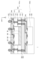
도 1a는 실시예에 따른 반도체 패키지의 제조 과정을 도시한 평면도이다. 도 1b는 실시예에 따른 제1 패키지를 도시한 평면도이다. 도 2a 내지 도 2f는 실시예에 따른 반도체 패키지의 제조 과정을 설명하기 위한 단면도들이다. 도 2a 내지 도 2e는 도 1a의 Ⅰ-Ⅰ'선을 따라 자른 단면들에 대응되고, 도 2f 및 도 2g는 도 1b의 Ⅱ-Ⅱ' 선을 따른 단면들에 대응된다. 1A is a plan view showing a manufacturing process of a semiconductor package according to an embodiment. Figure 1B is a plan view showing a first package according to an embodiment. 2A to 2F are cross-sectional views for explaining the manufacturing process of a semiconductor package according to an embodiment. FIGS. 2A to 2E correspond to cross-sections taken along line I-I' of FIG. 1A, and FIGS. 2f and 2g correspond to cross-sections taken along line II-II' of FIG. 1B.
도 1a 및 도 2a를 참조하면, 연결 기판(200)이 캐리어 기판(100) 상에 제공될 수 있다. 연결 기판(200)은 캐리어 접착층(150)에 의해 캐리어 기판(100) 상에 부착될 수 있다. 연결 기판(200)은 그 내부를 관통하는 홀(290)을 가질 수 있다. 연결 기판(200)은 베이스층들(210) 및 상기 베이스층들(210) 내의 도전부(220)를 포함할 수 있다. 일 예로, 인쇄회로기판(PCB)이 연결 기판(200)으로 사용될 수 있다. 도전부(220)는 하부 패드들(221), 배선 패턴(222), 비아들(223), 및 상부 패드들(224)을 포함할 수 있다. 하부 패드들(221)은 연결 기판(200)의 하면(200b) 상에 배치될 수 있다. 비아들(223)은 베이스층들(210) 중에서 적어도 하나를 관통할 수 있다. 배선 패턴(222)은 베이스층들(210) 사이에 개재되며, 비아들(223)과 접속할 수 있다. 상부 패드들(224)은 연결 기판(200)의 상면 상에 제공되며, 비아들(223) 중에서 적어도 하나와 접속할 수 있다. 상부 패드들(224)은 배선 패턴(222) 및 비아들(223)을 통해 하부 패드들(221)과 전기적으로 연결될 수 있다. 상부 패드들(224)은 하부 패드들(221)과 제3 방향(D3)을 따라 정렬되지 않을 수 있다. 여기에서, 제3 방향(D3)은 연결 기판(200)의 하면(200b)에 수직한 방향으로, 제1 방향(D1) 및 제2 방향(D2)은 연결 기판(200)의 하면(200b)과 나란한 방향으로 정의될 수 있다. 제1 방향(D1)은 제2 방향(D2)과 교차할 수 있다. Referring to FIGS. 1A and 2A , a
도 1a 및 도 2b를 참조하면, 제1 반도체칩(300)이 캐리어 기판(100) 상에 제공될 수 있다. 제1 반도체칩(300)은 연결 기판(200)의 홀(290) 내에 제공될 수 있다. 제1 반도체칩(300)은 그 하면(300b) 상에 배치된 제1 칩 패드들(301)을 포함할 수 있다. 제1 칩 패드들(301)은 캐리어 기판(100)을 향할 수 있다. 제1 반도체칩(300)은 실리콘을 포함할 수 있다.Referring to FIGS. 1A and 2B , a
금속층(ML)이 제1 반도체칩(300) 상에 배치될 수 있다. 금속층(ML)은 구리 또는 알루미늄을 포함할 수 있다. 금속층(ML)은 15μm 내지 25 μm의 두께(T1)를 가질 수 있다. 금속층(ML)은 비교적 높은 모듈러스를 가질 수 있다. 예를 들어, 금속층(ML)은 50 GPa 이상, 상세하게는, 50 GPa 내지 200 GPa의 모듈러스를 가질 수 있다. 이 때, 모듈러스는 영의 모듈러스(Young’s modulus)를 의미하며, 물체에 압력을 가했을 때, 영스 모듈러스가 높을수록 그 물체의 변형 정도는 작을 수 있다. 제1 반도체칩(300) 및 금속층(ML) 사이에 접착층(350)이 형성되어, 금속층(ML)이 제1 반도체칩(300)에 부착될 수 있다. 이하, 금속층(ML)의 형성에 대하여 보다 상세하게 설명한다. A metal layer ML may be disposed on the
도 3a는 실시예에 따른 금속층의 형성 공정을 설명하기 위한 평면도이다. 도 3b 내지 도 3d는 금속층의 형성과정을 도시한 단면도들로, 도 3a의 Ⅲ-Ⅲ'선을 따라 자른 단면들에 대응된다. Figure 3a is a plan view for explaining a metal layer forming process according to an embodiment. FIGS. 3B to 3D are cross-sectional views showing the formation process of the metal layer, and correspond to cross-sections taken along line III-III' in FIG. 3A.
도 3a 및 도 3b를 참조하면, 제1 반도체칩(300)을 포함하는 반도체 기판(1300)이 제공될 수 있다. 제1 반도체칩(300)은 반도체 기판(1300) 내에 복수로 제공될 수 있다. 반도체 기판(1300)은 실리콘과 같은 반도체로 만들어진 웨이퍼 레벨의 기판일 수 있다. 제1 반도체칩(300)은 제1 칩 패드들(301)을 가질 수 있다. Referring to FIGS. 3A and 3B , a semiconductor substrate 1300 including a
도 3a 및 도 3c를 참조하면, 금속층(ML)이 반도체 기판(1300) 상에 제공되어, 제1 반도체칩들(300)의 상면들을 덮을 수 있다. 금속층(ML)의 평면적 형상은 반도체 기판(1300)의 평면적 형상과 다른 것으로 도시되었으나, 이에 제한되지 않는다. 접착층(350)은 제1 반도체칩들(300) 및 금속층(ML) 사이에 형성될 수 있다. 접착층(350)은 열경화성 폴리머 또는 열가소성 폴리머일 수 있다. 예를 들어, 접착층(350)은 150℃ 이상, 상세하게, 150℃ 내지 250℃로 가열된 후, 상온(예를 들어, 대략 0℃ 내지 50℃)으로 냉각될 수 있다. 상기 가열 및 냉각 과정에 의해 접착층(350)은 경화 또는 소성 변형(plastic deformation)되어, 굳어질(solidify) 수 있다. 다른 예로, 접착층(350)은 생략되고, 제1 반도체칩들(300) 상에 씨드층(미도시)가 형성될 수 있다. 씨드층은 티타늄을 포함할 수 있다. 금속층(ML)은 스퍼터링 또는 도금법에 의해 상기 씨드층 상에 형성될 수 있다. 또 다른 예로, 금속층(ML)은 스프레이 코팅, 보다 상세하게 콜드 스프레이 공정에 의해 형성될 수 있다. 이 경우, 접착층(350) 또는 씨드층은 형성되지 않고, 금속층(ML)은 제1 반도체칩들(300)과 직접 물리적으로 접촉할 수 있다. Referring to FIGS. 3A and 3C , a metal layer ML may be provided on the semiconductor substrate 1300 to cover the top surfaces of the
도 3a 및 도 3d를 참조하면, 금속층(ML) 및 반도체 기판(도 3c에서 1300)이 쏘잉되어, 제1 반도체칩들(300)이 서로 분리될 수 있다. 쏘잉된 후, 각각의 제1 반도체칩들(300)의 너비(W1)는 그 상면 상의 금속층(ML)의 너비(W2)와 동일할 수 있다. 이하, 단수의 제1 반도체칩(300)에 대하여 기술한다. Referring to FIGS. 3A and 3D , the metal layer ML and the semiconductor substrate (1300 in FIG. 3C ) are sawed so that the
다시 도 2b를 도 3c와 함께 참조하면, 그 상면 상에 금속층(ML)이 제공된 제1 반도체칩(300)이 캐리어 기판(100) 상에 배치될 수 있다. 제1 반도체칩(300)은 그 상면 상의 금속층(ML)과 실질적으로 동시에 캐리어 기판(100) 상에 배치될 수 있다. 그러나, 제1 반도체칩(300) 및 금속층(ML)의 형성은 도 3a 내지 도 3c에서 설명한 방법에 제한되지 않고, 다양할 수 있다. 일 예로, 제1 반도체칩(300)이 캐리어 기판(100) 상에 배치된 후, 별도의 금속층(ML)이 제1 반도체칩(300) 상에 배치될 수 있다. 이 때, 금속층(ML)의 너비(W2)는 그와 대응되는 제1 반도체칩(300)의 너비(W1)와 동일 또는 상이할 수 있다. 다른 예로, 도 2b의 제1 반도체칩(300)의 배치는 도 2a의 연결 기판(200)의 배치 이전에 수행될 수 있다. 이 경우, 제1 반도체칩(300)이 캐리어 기판(100) 상에 배치되고, 홀(290)이 제1 반도체칩(300)과 정렬되도록, 연결 기판(200)이 캐리어 기판(100) 상에 배치될 수 있다. Referring again to FIG. 2B together with FIG. 3C, a
도 1a 및 도 2c를 참조하면, 제1 몰딩막(400)이 캐리어 기판(100) 상에 형성될 수 있다. 제1 몰딩막(400)은 연결 기판(200)의 상면 및 금속층(ML)의 상면을 덮을 수 있다. 제1 몰딩막(400)은 연결 기판(200)과 금속층(ML) 사이의 갭 및 연결 기판(200)과 제1 반도체칩(300) 사이의 갭에 제공될 수 있다. 제1 몰딩막(400)은 절연성 폴리머, 예를 들어, 에폭시계 폴리머를 포함할 수 있다. 개구부(401)가 제1 몰딩막(400) 내에 형성되어, 상부 패드들(224)을 노출시킬 수 있다. 다른 예로, 개구부(401)는 형성되지 않을 수 있다. 점선으로 도시한 바와 같이, 캐리어 기판(100) 및 캐리어 접착층(150)이 제거되어, 제1 반도체칩(300)의 하면(300b) 및 연결 기판(200)의 하면(200b)이 노출될 수 있다. Referring to FIGS. 1A and 2C , the
도 1a 및 도 2d를 참조하면, 절연 패턴들(510) 및 도전 패턴(520)이 제1 반도체칩(300)의 하면(200b) 및 연결 기판(200)의 하면(300b) 상에 형성되어, 제1 기판(500)이 제조될 수 있다. 제1 기판(500)은 재배선 기판일 수 있다. 도전 패턴(520)은 절연 패턴들(510) 사이의 도전층 및 절연 패턴들(510)을 관통하는 비아를 포함할 수 있다. 도전 패턴(520)은 제1 반도체칩(300)의 제1 칩 패드들(301) 및 연결 기판(200)의 하부 패드들(221)과 접속할 수 있다. 보호층(511)이 제1 기판(500)의 하면 상에 형성될 수 있다. 일 예로, 보호층(511)은 제1 몰딩막(400)과 동일할 물질을 포함할 수 있다. 그러나 보호층(511)의 물질은 이에 제한되지 않는다. 재배선 기판이 제1 기판(500)으로 사용되므로, 제1 기판(500)은 인쇄회로기판보다 얇은 두께(T2)를 가질 수 있다. 예를 들어, 제1 기판(500)은 0.01mm 이하, 바람직하게는, 0.02mm 이하의 두께(T2)를 가질 수 있다. 이에 따라, 반도체 패키지가 소형화될 수 있다.1A and 2D, insulating
외부 단자들(550)이 제1 기판(500)의 하면 상에 형성되어, 도전 패턴(520)과 접속할 수 있다. 외부 단자들(550)은 상부 패드들(224)과 제3 방향(D3)으로 정렬되지 않을 수 있다. 외부 단자들(550)의 개수는 상부 패드들(224)의 개수와 다를 수 있다. 외부 단자들(550)은 도전 패턴(520), 하부 패드들(221), 배선 패턴(222), 및 비아들(223)에 의해 상부 패드들(224)과 전기적으로 연결될 수 있다. 배선 패턴(222)이 연결 기판(200) 내에 제공되어, 상부 패드들(224)은 하부 패드들(221)과 제3 방향(D3)을 따라 정렬되지 않을 수 있다. 이에 따라, 제1 기판(500) 내의 도전 패턴(520)의 배치 및 개수에 대한 제약이 감소할 수 있다. 제1 기판(500)이 더욱 얇은 두께(T2)를 가질 수 있다.
도전 패턴(520)은 제1 반도체칩(300)보다 높은 열팽창계수를 가질 수 있다 예를 들어, 도전 패턴(520)은 대략 25ppm/℃의 열팽창계수를 가지고, 제1 반도체칩(300)은 대략 3 ppm/℃의 열팽창계수를 가질 수 있다. 도전 패턴(520) 및 제1 반도체칩(300)의 열팽창계수의 차이(CTE mismatch)에 의해, 반도체 패키지의 휨(warpage)이 발생할 수 있다. 실시예들에 따르면, 금속층(ML)의 열팽창계수는 제1 반도체칩(300)의 열팽창계수보다 높고, 도전 패턴(520)의 열팽창계수와 유사할 수 있다. 예를 들어, 금속층(ML)은 대략 25ppm/℃ 내지 50ppm/℃의 열팽창계수를 가질 수 있다. 금속층(ML)은 제1 반도체칩(300)을 사이에 두고 도전 패턴(520)과 대향될 수 있다. 제1 반도체칩(300) 및 도전 패턴(520)의 열팽창계수 차이(CTE mismatch)는 제1 반도체칩(300) 및 금속층(ML)의 열팽창계수 차이에 의해 상쇄될 수 있다. 이에 따라, 반도체 패키지의 휨이 방지될 수 있다. 실시예들에 따르면, 금속층(ML)은 높은 모듈러스(예를 들어, 50GPa 이상)를 가져, 반도체 패키지의 휨이 더욱 방지될 수 있다. 금속층(ML)이 25ppm/℃보다 낮은 열팽창계수를 가지거나, 50GPa보다 낮은 모듈러스를 가지거나, 또는 15μm보다 얇은 두께를 가지면, 금속층(ML)은 반도체 패키지의 휨을 방지하기 어려울 수 있다. 이와 달리, 금속층(ML)이 50ppm/℃보다 높은 열팽창계수를 가지거나 또는 25μm보다 두꺼운 두께를 가지면, 금속층(ML)과 제1 반도체칩(300)의 열팽창계수의 차이가 과도하게 클 수 있다. 이 경우, 금속층(ML)과 제1 반도체칩(300)의 열팽창계수의 차이에 의해 반도체 패키지의 휨이 발생할 수 있다. The
실시예들에 따르면, 접착층(350)은 도 2b에서 설명한 바와 같이 경화 또는 소성 변형되어, 딱딱할 수 있다. 접착층(350)에 의해 반도체 패키지의 휨이 더욱 방지될 수 있다. According to embodiments, the
금속층(ML)은 제1 반도체칩(300)보다 높은 열전도율을 가질 수 있다. 예를 들어, 금속층(ML)은 140W/mk 이상, 상세하게는, 140 W/mk 내지 300 W/mk 의 열전도율을 가질 수 있다 반도체 패키지 동작 시, 제1 반도체칩(300)에서 발생한 열은 ㄱ금속층(ML)을 통해 외부로 빠르게 방출될 수 있다. 이에 따라 반도체 패키지의 동작 신뢰성이 향상될 수 있다. 접착층(350)이 5μm보다 두꺼우면 제1 반도체칩(300)에서 발생한 열이 금속층(ML)으로 비교적 느리게 전달될 수 있다. 실시예들에 따르면, 접착층(350)은 0.01μm 내지 5μm의 두께(T3)를 가질 수 있다. The metal layer ML may have higher thermal conductivity than the
도 1a, 도 1b, 및 도 2e를 참조하면, 제1 기판(500) 및 연결 기판(200)이 쏘잉되어, 제1 패키지들(P100)이 형성될 수 있다. 제1 패키지들(P100) 각각은 도 1b와 같은 단면을 가질 수 있다. 제1 패키지(P100)의 연결 기판(200)은 홀(290)을 가질 수 있다. Referring to FIGS. 1A, 1B, and 2E, the
도 1b 및 도 2f를 참조하면, 제2 패키지(P200)가 도 2e의 제1 패키지(P100) 상에 실장되어, 반도체 패키지(1)가 제조될 수 있다. 제2 패키지(P200)는 제2 기판(700), 제2 반도체칩(800), 및 제2 몰딩막(900)을 포함할 수 있다. 제2 반도체칩(800)은 제2 기판(700) 상에 플립칩 실장될 수 있다. 도시된 바와 달리, 제2 반도체칩(800)은 본딩 와이어(미도시)에 의해 제2 기판(700)과 전기적으로 연결될 수 있다. 제2 몰딩막(900)이 제2 기판(700) 상에서 제2 반도체칩(800)을 덮을 수 있다. 제2 기판(700)의 하면 상에 연결 단자들(690)이 제공될 수 있다. 연결 단자들(690)이 상부 패드들(224)과 접속하여, 제2 패키지(P200)가 제1 패키지(P100)와 전기적으로 연결될 수 있다. Referring to FIGS. 1B and 2F , the second package P200 is mounted on the first package P100 of FIG. 2E to manufacture the
도 2g는 실시예에 따른 반도체 패키지를 도시한 단면도이다. 이하, 앞서 설명한 바와 중복되는 내용은 생략한다. Figure 2g is a cross-sectional view showing a semiconductor package according to an embodiment. Hereinafter, content that overlaps with what was previously described will be omitted.
도 2g를 참조하면, 반도체 패키지(2)는 적층된 제1 패키지(P100), 제3 패키지(P300), 및 제2 패키지(P200)를 포함할 수 있다. 제1 패키지(P100)는 도 1a 내지 도 2e에서 설명한 바와 같이 제조될 수 있다. 제3 패키지(P300)는 도 1a 내지 도 2e에서 설명한 제1 패키지(P100)와 동일한 방법에 의해 제조될 수 있다. 예를 들어, 제3 기판(500'), 제3 반도체칩(300'), 상부 접착층(350'), 상부 연결 기판(200'), 제3 몰딩막(400'), 및 금속층(ML')은 제1 기판(500), 제1 반도체칩(300), 접착층(350), 연결 기판(200), 제1 몰딩막(400), 및 금속층(ML)과 실질적으로 동일할 수 있다. 상부 베이스층들(210') 및 상부 도전부(220')는 도 2a의 베이스층들(210) 및 도전부(220)와 실질적으로 동일할 수 있다. 제1 패키지(P100) 및 제3 패키지(P300) 사이에 제1 연결 단자들(691)이 제공될 수 있다. 제1 연결단자들(691)은 상부 패드들(224) 및 제3 도전 패턴(520')과 접속할 수 있다. 제3 패키지(P300)는 제1 패키지(P100) 상에 단수개 제공되는 것으로 도시되었으나, 이와 달리, 제3 패키지(P300)는 복수 개 제공될 수 있다. Referring to FIG. 2G, the semiconductor package 2 may include a first package (P100), a third package (P300), and a second package (P200) that are stacked. The first package (P100) may be manufactured as described in FIGS. 1A to 2E. The third package (P300) may be manufactured by the same method as the first package (P100) described in FIGS. 1A to 2E. For example, the third substrate 500', the third semiconductor chip 300', the upper adhesive layer 350', the upper connection substrate 200', the third molding film 400', and the metal layer ML'. ) may be substantially the same as the
제2 패키지(P200)가 제3 패키지(P300) 상에 배치될 수 있다. 제2 패키지(P200)는 제2 기판(700), 제2 반도체칩(800), 및 제2 몰딩막(900)을 포함할 수 있다. 제2 패키지(P200) 및 제3 패키지(P300) 사이에 제2 연결 단자들(692)이 제공될 수 있다. 제2 패키지(P200)는 제2 연결 단자들(692)에 의해 제3 패키지(P300)과 전기적으로 연결될 수 있다. The second package (P200) may be placed on the third package (P300). The second package P200 may include a
도 4a는 실시예에 따른 제1 패키지를 도시한 평면도이다. 도 4b 및 도 4c는 실시예에 따른 제1 패키지의 제조 방법을 도시한 단면도들로, 도 4a의 Ⅳ-Ⅳ'선을 따라 자른 단면들에 대응된다. 이하에서, 설명의 간소화를 위하여, 단수의 제1 패키지의 제조에 대하여 도시 및 설명한다. 그러나, 아래의 실시예들이 웨이퍼 레벨의 제1 패키지의 제조를 배제하는 것은 아니다. 이하, 앞서 설명한 바와 중복되는 내용은 생략한다. Figure 4a is a plan view showing a first package according to an embodiment. FIGS. 4B and 4C are cross-sectional views showing a method of manufacturing a first package according to an embodiment, and correspond to cross-sections taken along line IV-IV' of FIG. 4A. Below, for the sake of simplicity of explanation, the manufacturing of a single first package is shown and described. However, the embodiments below do not exclude fabrication of the first package at the wafer level. Hereinafter, content that overlaps with what was previously described will be omitted.
도 4a 및 도 4b를 참조하면, 연결 기판(201) 및 제1 반도체칩(300)이 캐리어 기판(100) 상에 제공될 수 있다. 도 4a에 도시된 바와 같이, 연결 기판(201)은 사각형 형상을 가질 수 있다. 연결 기판(201)은 복수로 제공될 수 있다. 연결 기판들(201)은 제1 반도체칩(300)을 둘러싸며 배치될 수 있다. 도 4b와 같이, 연결 기판들(201) 각각은 베이스층(210) 및 도전부(220)를 포함할 수 있다. 도전부(220)는 하부 패드들(221), 비아들(223), 및 상부 패드들(224)을 포함할 수 있다. 도 2a의 연결 기판(200)과 달리, 배선 패턴(도 2a에서 222)는 생략되고, 비아들(223)은 하부 패드들(221) 및 상부 패드들(224)과 직접 접속할 수 있다. 비아들(223)은 베이스층(210)을 관통할 수 있다. 연결 기판들(201)은 제1 반도체칩(300)이 배치되기 이전 또는 이후에 캐리어 기판(100) 상에 배치될 수 있다. 금속층(ML)이 접착층(350)에 의해 제1 반도체칩(300) 상에 부착될 수 있다. 제1 반도체칩(300), 접착층(250), 및 금속층(ML)은 도 3a 내지 도 3d에서 설명한 바와 실질적으로 동일할 수 있다. 제1 몰딩막(400)은 제1 반도체칩(300) 및 금속층(ML)의 갭에 형성될 수 있다. 캐리어 기판(100) 및 캐리어 접착층(150)이 제거되고, 제1 반도체칩(300)의 하면(300b) 및 연결 기판들(200)의 하면들(201b)이 노출될 수 있다. Referring to FIGS. 4A and 4B , a connection substrate 201 and a
도 4a 및 도 4c를 참조하면, 제1 기판(500)이 제1 반도체칩(300)의 하면(300b) 및 연결 기판들(201)의 하면들(201b) 상에 형성되어, 제1 패키지(P101)이 제조될 수 있다. 제1 기판(500)은 절연 패턴들(510) 및 도전 패턴(520)을 포함할 수 있다. 외부 단자들(550)이 제1 기판(500)의 하면 상에 형성되어, 도전 패턴(520)과 접속할 수 있다. 제1 기판(500) 및 외부 단자들(550)의 형성 방법 및 전기적 연결은 도 2d에서 설명한 바와 동일할 수 있다. Referring to FIGS. 4A and 4C, the
도 5a는 실시예에 따른 제1 패키지를 도시한 단면도이다. 이하 앞서 설명한 바와 중복되는 내용은 생략한다. Figure 5a is a cross-sectional view showing a first package according to an embodiment. Hereinafter, content that overlaps with what was previously described will be omitted.
도 5a를 참조하면, 제1 패키지(P102)는 제1 기판(500), 제1 반도체칩(300), 연결 기판(200), 및 접착층(350), 및 제1 몰딩막(400)을 포함할 수 있다. 제1 기판(500), 제1 반도체칩(300), 및 연결 기판(200)은 도 1a 내지 도 2e에서 설명한 바와 실질적으로 동일한 방법에 의해 형성될 수 있다. 금속층(ML)의 상면 상에 상부 탄소층(360)이 제공될 수 있다. 상부 탄소층(360)은 카본 나노튜브, 그래핀, 또는 그라파이트를 포함할 수 있다. 일 예로, 상부 탄소층(360)이 금속층(ML) 상면 상에 직접 성장되고, 상기 금속층(ML)이 제1 반도체칩(300) 상에 배치될 수 있다. 이 경우, 상부 탄소층(360)의 너비 및 평면적 형상은 금속층(ML)의 너비 및 평면적 형상과 동일할 수 있다. 다른 예로, 상부 탄소층(360)은 모기판(미도시) 상에 성장된 후, 금속층(ML) 상에 제공될 수 있다. 상부 탄소층(360)은 제1 반도체칩(300)보다 높은 열전도율을 가질 수 있다. 이에 따라, 제1 패키지(P102) 동작 시, 제1 반도체칩(300)에서 발생하는 열이 금속층(ML) 및 상부 탄소층(360)을 통해 보다 빠르게 방출될 수 있다. 제1 반도체칩(300) 및 접착층(350) 사이에 하부 탄소층(미도시)이 더 개재될 수 있다. Referring to FIG. 5A, the first package (P102) includes a
제1 몰딩막(400)은 연결 기판(200)의 상면 및 상부 탄소층(360)의 상면을 덮을 수 있다. 제1 몰딩막(400)은 도전부(220)의 상면, 예를 들어, 상부 패드들(224)을 노출시키는 개구부들(401)을 가질 수 있다. 다른 예로, 개구부(401)는 생략될 수 있다. 제1 몰딩막(400)은 제1 반도체칩(300) 및 연결 기판(200)의 내측면(200c) 사이의 갭으로 연장될 수 있다. 제1 몰딩막(400)은 연결 기판(200)의 외측면(200d)을 덮지 않을 수 있다. 연결 기판(200)의 외측면(200d)은 연결 기판(200)의 내측면(200c)과 대향될 수 있다. The
도 5b는 실시예에 따른 제1 패키지를 도시한 단면도이다. 이하 앞서 설명한 바와 중복되는 내용은 생략한다.Figure 5b is a cross-sectional view showing a first package according to an embodiment. Hereinafter, content that overlaps with what was previously described will be omitted.
도 5b를 참조하면, 제1 패키지(P103)는 제1 기판(500), 제1 반도체칩(300), 연결 기판(200), 제1 몰딩막(400), 접착층(350)을 포함할 수 있다. 제1 반도체칩(300)은 그 내부에 발열원들(미도시)을 포함할 수 있다. 발열원들은 중앙 처리 장치(CPU), 메모리 인터페이스, 및 범용 직렬 버스(USB) 등과 같은 IP 블럭(IP Block)일 수 있다. IP 블럭은 반도체 직접회로를 구성하기 위해 필요한 기능을 하드웨어 또는 소프트웨어 상태로 정리한 블럭을 의미한다. 제1 반도체칩(300)의 동작 시, 발열원들 중에서 특정 열량 이상의 많은 열을 발생시키는 것을 핫 스팟(370)으로 정의될 수 있다. Referring to FIG. 5B, the first package (P103) may include a
리세스(380)가 제1 반도체칩(300)의 상면 상에 제공될 수 있다. 금속층(ML)은 상기 리세스(380) 내로 연장된 돌출부(MLP)를 포함할 수 있다. 예를 들어, 리세스(380), 금속층(ML), 및 돌출부(MLP)는 도 3a 및 도 3b의 웨이퍼 레벨의 제1 반도체칩(300) 상에 형성될 수 있다. 금속층(ML)이 제공된 제1 반도체칩(300)을 사용하여, 제1 패키지(P103)가 제조될 수 있다. 돌출부(MLP)는 핫 스팟(370)과 인접하여 배치될 수 있다. 일 예로, 돌출부(MLP)는 핫 스팟(370)과 제3 방향(D3)으로 정렬될 수 있다. 돌출부(MLP)의 단면의 형상 및 개수는 도시된 바에 한정되지 않고, 다양할 수 있다. 금속층(ML)이 돌출부(MLP)를 포함하여, 금속층(ML) 및 핫 스팟(370) 사이의 거리가 짧을 수 있다. 제1 반도체칩(300) 동작 시, 핫 스팟(370)에서 발생하는 열은 돌출부(MLP)를 통해 금속층(ML)으로 빠르게 전달될 수 있다. 이에 따라, 제1 반도체칩(300)의 동작 신뢰성이 더욱 향상될 수 있다. 금속층(ML)과 제1 반도체칩(300) 사이 및 돌출부(MLP)와 제1 반도체칩(300) 사이에 접착층(350)이 개재될 수 있다. 다른 예로, 접착층(350)은 생략될 수 있다. A recess 380 may be provided on the top surface of the
도 5c는 실시예에 따른 제1 패키지를 도시한 단면도이다. 이하 앞서 설명한 바와 중복되는 내용은 생략한다.Figure 5C is a cross-sectional view showing a first package according to an embodiment. Hereinafter, content that overlaps with what was previously described will be omitted.
도 5c를 참조하면, 제1 패키지(P104)는 제1 기판(500), 제1 하부 반도체칩(310), 제1 상부 반도체칩(320), 연결 기판(200), 제1 몰딩막(400), 접착층(350), 및 금속층(ML)을 포함할 수 있다. Referring to FIG. 5C, the first package (P104) includes a
제1 하부 반도체칩(310) 및 제1 상부 반도체칩(320)은 앞서 설명한 제1 반도체칩(300)과 실질적으로 동일한 물질을 포함할 수 있다. 제1 하부 반도체칩(310) 및 제1 상부 반도체칩(320)은 제1 기판(500) 상에서 연결 기판(200)의 홀(290) 내에 배치될 수 있다. 제1 하부 칩 패드(311)는 제1 하부 반도체칩(310)의 하면 상에 배치되며, 도전 패턴(520)과 접속할 수 있다. 제1 하부 반도체칩(310)은 그 내부를 관통하며, 제1 하부 칩 패드(311)와 접속하는 쓰루 비아(312)를 포함할 수 있다. 제1 상부 반도체칩(320)이 제1 하부 반도체칩(310) 상에 적층될 수 있다. 제1 상부 반도체칩(320)은 그 하면 상에 제1 상부 칩 패드(321)를 가질 수 있다. 제1 상부 칩 패드(321)는 쓰루 비아(312)와 접속하여, 제1 상부 반도체칩(320)이 제1 기판(500)과 전기적으로 연결될 수 있다. The first lower semiconductor chip 310 and the first upper semiconductor chip 320 may include substantially the same material as the
금속층(ML)이 제1 상부 반도체칩(320) 상에 배치될 수 있다. 금속층(ML)은 제1 반도체칩들(310, 320)보다 높은 열전도율 및 높은 열팽창계수를 가질 수 있다. 금속층(ML)은 제1 패키지(P104)의 휨을 방지/감소시킬 수 있다. The metal layer ML may be disposed on the first upper semiconductor chip 320 . The metal layer ML may have a higher thermal conductivity and a higher coefficient of thermal expansion than the first semiconductor chips 310 and 320. The metal layer ML may prevent/reduce bending of the first package P104.
도 5d 및 도 5e는 실시예들에 따른 제1 패키지를 각각 도시한 단면도들이다.FIGS. 5D and 5E are cross-sectional views each showing a first package according to embodiments.
도 5d 및 도 5e를 참조하면, 제1 패키지(P105, P106)는 제1 기판(500), 제1 반도체칩(300), 연결 기판(200), 제1 몰딩막(400), 접착층(350), 및 금속층(ML)을 포함할 수 있다. 제1 기판(500), 제1 몰딩막(400), 연결 기판(200), 및 금속층(ML)은 도 1a 내지 도 2e에서 설명한 바와 실질적으로 동일한 방법에 의해 형성될 수 있다. 제1 반도체칩(300)은 연결 기판(200)의 홀(290) 내에 복수로 제공될 수 있다. 제1 반도체칩들(300)은 서로 제1 방향(D1)으로 이격될 수 있다. Referring to FIGS. 5D and 5E, the first package (P105, P106) includes a
도 5d와 같이, 금속층(ML)은 단수로 제공되며, 제1 반도체칩(300)을 덮을 수 있다. 금속층(ML)의 너비(W2)는 제1 반도체칩들(300)의 너비들(W2)의 합과 동일하거나 더 넓을 수 있다. As shown in FIG. 5D, the metal layer ML is provided singly and can cover the
도 5e와 같이 금속층(ML)은 복수로 제공될 수 있다. 각 금속층들(ML)은 각 제1 반도체칩들(300) 상에 제공될 수 있다. 각 금속층(ML) 너비(W2)는 대응되는 각 제1 반도체칩(300)의 너비(W1)와 동일할 수 있다. As shown in FIG. 5E, multiple metal layers ML may be provided. Each metal layer ML may be provided on each
도 6a 내지 6c는 실시예에 따른 반도체 패키지의 제조를 도시한 단면도들이다. 이하, 앞서 설명한 바와 중복되는 내용은 생략한다. 6A to 6C are cross-sectional views showing the manufacturing of a semiconductor package according to an embodiment. Hereinafter, content that overlaps with what was previously described will be omitted.
도 6a를 참조하면, 제1 반도체칩(300), 연결 기판(200), 제1 몰딩막(400), 및 금속층(ML)이 캐리어 기판(100) 상에 배치될 수 있다. 도전부(220)는 접지 패턴(220G) 및 신호 패턴(220S)을 포함할 수 있다. 접지 패턴(220G)은 하부 접지 패드들(221G), 접지 배선 패턴(222G), 접지 비아들(223G), 및 상부 접지 패드들(224G)을 포함할 수 있다. 신호 패턴(220S)은 하부 신호 패드(221S), 신호 배선 패턴(222S), 신호 비아들(223S), 및 상부 신호 패드(224S)를 포함할 수 있다. 신호 패턴(220S)은 접지 패턴(220G)과 절연될 수 있다. 하부 패드들(221G, 221S) 및 상부 패드들(224G, 224S)은 연결 기판(200)의 하면(200b) 및 상면 상에 각각 제공될 수 있다. 배선 패턴들(222G, 222S)은 베이스층들(210) 사이에 개재될 수 있다. 비아들(223G, 223S)은 베이스층들(210) 중 적어도 하나를 관통할 수 있다. Referring to FIG. 6A , the
제1 반도체칩(300)은 제1 접지 칩 패드(301G) 및 제1 신호 칩 패드(301S)를 포함할 수 있다. 제1 접지 칩 패드(301G)는 제1 신호 칩 패드(301S)와 절연될 수 있다. 제1 몰딩막(400)은 연결 기판(200)의 상면 및 제1 반도체칩(300)의 측면 상에 제공되나, 제1 반도체칩(300)의 상면 및 상부 패드들(224G, 224S)의 상면들을 덮지 않을 수 있다. The
금속층(ML)이 제1 반도체칩(300)의 상면 상에 배치될 수 있다. 금속층(ML)은 도 2b에서 설명한 동일한 두께 및 모듈러스 그리고 도 2d에서 설명한 바와 같은 열팽창계수 및 열전도율을 가질 수 있다. 금속층(ML)의 너비(W2)는 제1 반도체칩(300)의 너비(W1)보다 넓을 수 있다. 금속층(ML)은 연결 기판(200)의 상부 접지 패드들(224G) 중에서 어느 하나 상으로 연장되어, 상기 상부 접지 패드들(224G) 중 어느 하나와 접속할 수 있다. 금속층(ML)은 상부 접지 패드들(224G) 중 다른 하나를 덮지 않을 수 있다. 금속층(ML)은 상부 신호 패드(224S)와 제1 방향(D1)으로 이격되며, 상부 신호 패드(224S)와 절연될 수 있다. 이후, 캐리어 기판(100) 및 캐리어 접착층(150)이 제거될 수 있다. The metal layer ML may be disposed on the top surface of the
도 6b를 참조하면, 제1 기판(500)이 제1 반도체칩(300)의 하면 및 연결 기판(200)의 하면 상에 형성되어, 제1 패키지(P107)가 제조될 수 있다. 제1 기판(500)은 절연 패턴들(510), 접지 도전 패턴(520G), 및 신호 도전 패턴(520S)을 포함할 수 있다. 도전 패턴들(520G, 520S)은 도 2d의 도전 패턴(520)과 동일한 방법에 의해 형성될 수 있다. 접지 도전 패턴(520G)은 제1 접지 칩 패드(301G) 및 하부 접지 패드들(221G)과 접속할 수 있다. 신호 도전 패턴(520S)은 제1 신호 칩 패드(301S) 및 하부 신호 패드(221S)와 접속할 수 있다. 신호 도전 패턴(520S)은 접지 도전 패턴(520G)과 절연될 수 있다. Referring to FIG. 6B, the
외부 단자들(550G, 550S)이 제1 기판(500)의 하면 상에 형성될 수 있다. 외부 단자들(550G, 550S)의 형성 및 배치는 도 2d에서 설명한 바와 실질적으로 동일할 수 있다. 외부 단자들(550G, 550S)은 접지 단자(550G) 및 신호 단자(550S)를 포함할 수 있다. 접지 단자(550G) 및 신호 단자(550S)는 접지 도전 패턴(520G) 및 신호 도전 패턴(520S)과 각각 접속할 수 있다. 금속층(ML)은 접지 패턴(220G), 접지 도전 패턴(520G), 및 접지 단자(550G)에 의해 접지될 수 있다. 다른 예로, 제1 기판(500)이 형성된 후, 금속층(ML)이 제1 반도체칩(300) 상에 배치될 수 있다. External terminals 550G and 550S may be formed on the lower surface of the
도 6c를 참조하면, 제2 기판(700), 제2 반도체칩(800), 및 제2 몰딩막(900)을 포함하는 제2 패키지(P200)가 준비될 수 있다. 제2 반도체칩(800)은 제2 접지 칩 패드(801G) 및 제2 신호 칩 패드(801S)를 가질 수 있다. 제2 기판(700)은 상부 접지 패턴(720G) 및 상부 신호 패턴(720S)을 포함할 수 있다. 상부 접지 패턴(720G) 및 상부 신호 패턴(720S)은 및 제2 신호 칩 패드(801S)와 각각 접속할 수 있다. 접지 연결 단자(690G) 및 신호 연결 단자(690S)가 제2 기판(700)의 하면 상에 제공되어, 상부 접지 패턴(720G) 및 상부 신호 패턴(720S)과 각각 접속할 수 있다. Referring to FIG. 6C, a second package P200 including a
제2 패키지(P200)가 도 6b의 제1 패키지(P107) 상에 배치될 수 있다. 이 때, 신호 연결 단자(690S)는 제1 패키지(P108)의 상부 신호 패드(224S)와 정렬될 수 있다. 접지 연결 단자(690G)은 상부 접지 패드들(224G) 중에서 금속층(ML)에 의해 노출된 것과 정렬될 수 있다. 솔더링에 의해, 신호 연결 단자(690S)는 상부 신호 패드(224S)와 접속할 수 있다. 접지 연결 단자(690G)는 상부 접지 패드들(224G) 중에서 금속층(ML)에 의해 노출된 것과 접속할 수 있다. 이에 따라, 반도체 패키지(3)가 제조될 수 있다.The second package (P200) may be placed on the first package (P107) of FIG. 6B. At this time, the signal connection terminal 690S may be aligned with the upper signal pad 224S of the first package (P108). The ground connection terminal 690G may be aligned with one of the upper ground pads 224G exposed by the metal layer ML. By soldering, the signal connection terminal 690S can be connected to the upper signal pad 224S. The ground connection terminal 690G may be connected to one of the upper ground pads 224G exposed by the metal layer ML. Accordingly, the semiconductor package 3 can be manufactured.
도 7a 내지 도 7d는 실시예에 따른 반도체 패키지의 제조 과정을 도시한 단면도들이다. 이하, 앞서 설명한 바와 중복되는 내용은 생략한다. 7A to 7D are cross-sectional views showing the manufacturing process of a semiconductor package according to an embodiment. Hereinafter, content that overlaps with what was previously described will be omitted.
도 7a를 참조하면, 제1 기판(500), 제1 반도체칩(300), 연결 기판(200), 및 제1 몰딩막(400)이 제공될 수 있다. 제1 기판(500), 제1 반도체칩(300), 연결 기판(200), 및 제1 몰딩막(400)은 도 1a 내지 도 2e에서 설명한 바와 실질적으로 동일한 방법에 의해 형성될 수 있다. 다만, 제1 반도체칩(300)의 상면(300a)은 연결 기판(200)의 상면(200a)과 실질적으로 동일한 레벨에 배치될 수 있다. 도전부(220)는 접지 패턴(220G) 및 신호 패턴(220S)을 포함할 수 있다. 도전부(220)와 제1 기판(500)의 전기적 연결은 도 6a에서 설명한 바와 동일할 수 있다. 이하, 설명의 간소화를 위해 복수의 상부 신호 패드들(224S) 및 단수의 상부 접지 패드(224G)에 대하여 기술하나, 상부 신호 패드들(224S) 및 상부 접지 패드(224G)의 개수가 이제 제한되는 것은 아니다. Referring to FIG. 7A, a
도 7b를 참조하면, 절연층(610), 금속층들(ML1, ML2), 금속 패턴(620), 및 금속 비아들(630G, 630S)를 포함하는 인터포저층(600)이 준비될 수 있다. 절연층(610)은 폴리머를 포함할 수 있다. 일 예로, 플렉서블 필름이 절연층(610)으로 사용될 수 있다. 절연층(610)은 서로 대향하는 제1 면(610a) 및 제2 면(610b)을 가질 수 있다. 금속층들(ML1, ML2)은 인터포저층(600) 내에 제공될 수 있다. 금속층들(ML1, ML2)은 절연층(610)의 제1 면(610a) 상에 배치될 수 있다. 제1 금속층(ML1)은 제2 금속층(ML2)과 제1 방향(D1)으로 이격되며, 전기적으로 절연될 수 있다. 제1 및 제2 금속층들(ML1, ML2)은 앞서 금속층(ML)의 예에서 바와 동일한 두께, 모듈러스, 열팽창계수, 및 열전도율을 가질 수 있다. 금속 패턴(620)은 절연층(610)의 제1 면(610a) 상에 제공될 수 있다. 금속 패턴(620)은 금속층들(ML1, ML2)과 제1 방향(D1)으로 이격되며, 전기적으로 절연될 수 있다. 일 예로, 금속 패턴(620)은 금속층들(ML1, ML2)과 동일한 공정에 의하여 형성될 수 있다. 이에 따라, 금속 패턴(620)은 금속층들(ML1, ML2)과 동일한 물질을 포함하며, 실질적으로 동일한 두께를 가질 수 있다. Referring to FIG. 7B, an interposer layer 600 including an insulating layer 610, metal layers ML1 and ML2, a metal pattern 620, and metal vias 630G and 630S may be prepared. The insulating layer 610 may include polymer. As an example, a flexible film may be used as the insulating layer 610. The insulating layer 610 may have a first surface 610a and a second surface 610b facing each other. Metal layers ML1 and ML2 may be provided in the interposer layer 600 . The metal layers ML1 and ML2 may be disposed on the first side 610a of the insulating layer 610 . The first metal layer ML1 is spaced apart from the second metal layer ML2 in the first direction D1 and may be electrically insulated. The first and second metal layers ML1 and ML2 may have the same thickness, modulus, coefficient of thermal expansion, and thermal conductivity as in the previous example of the metal layer ML. A metal pattern 620 may be provided on the first side 610a of the insulating layer 610. The metal pattern 620 is spaced apart from the metal layers ML1 and ML2 in the first direction D1 and may be electrically insulated. For example, the metal pattern 620 may be formed through the same process as the metal layers ML1 and ML2. Accordingly, the metal pattern 620 may include the same material as the metal layers ML1 and ML2 and may have substantially the same thickness.
금속 비아들(630G, 630S)이 절연층(610) 내에 제공될 수 있다. 금속 비아들(630G, 630S)의 상면들은 절연층(610)에 의해 노출될 수 있다. 금속 접지 비아(630G)는 제1 금속층(ML1) 상에 제공되며, 제1 금속층(ML1)과 접속할 수 있다. 금속 신호 비아(630S)는 복수로 제공될 수 있다. 금속 신호 비아들(630S)은 제2 금속층(ML2) 및 금속 신호 패턴(620S) 상에 각각 제공되며, 제2 금속층(ML2) 및 금속 신호 패턴(620S)과 각각 접속할 수 있다. Metal vias 630G and 630S may be provided in the insulating layer 610. Top surfaces of the metal vias 630G and 630S may be exposed by the insulating layer 610. The metal ground via 630G is provided on the first metal layer ML1 and can be connected to the first metal layer ML1. A plurality of metal signal vias 630S may be provided. The metal signal vias 630S are provided on the second metal layer ML2 and the metal signal pattern 620S, respectively, and can be connected to the second metal layer ML2 and the metal signal pattern 620S, respectively.
도 7c를 참조하면, 도 7b의 인터포저층(600)이 도 7a의 연결 기판(200) 및 제1 반도체칩(300) 상에 배치될 수 있다. 이 때, 절연층(610)의 제1 면(610a)이 제1 반도체칩(300)의 상면을 향할 수 있다. 제1 금속층(ML1) 및 제2 금속층(ML2)은 제1 반도체칩(300)을 덮을 수 있다. 제1 금속층(ML1)은 상부 접지 패드(224G) 상으로 연장되어, 상부 접지 패드(224G)와 접속할 수 있다. 제2 금속층(ML2)은 제1 반도체칩(300) 상에서 상부 신호 패드들(224S) 중 어느 하나 상으로 연장되며, 상부 신호 패드들(224S) 중 어느 하나와 접속할 수 있다. 금속 패턴(620)은 상부 신호 패드들(224S) 중에서 다른 하나와 접속할 수 있다. 금속층들(ML1, ML2) 및 제1 반도체칩(300) 사이에 접착층(350)이 개재될 수 있다. 이에 따라, 제1 패키지(P108)가 제조될 수 있다. Referring to FIG. 7C, the interposer layer 600 of FIG. 7B may be disposed on the
도 7d를 참조하면, 제2 패키지(P200)가 도 7c의 제1 패키지(P108) 상에 실장되어, 반도체 패키지(4)가 제조될 수 있다. 제2 반도체칩(800)은 제2 기판(700)과 도 6c에서 설명한 바와 같이 전기적으로 연결될 수 있다. 제2 접지 칩 패드(801G) 및 제2 신호 칩 패드(801S)는 상부 접지 패턴(720G) 및 상부 신호 패턴(720S)과 각각 접속할 수 있다. 접지 연결 단자(690G) 및 신호 연결 단자(690S)이 제2 기판(700)의 하면 상에 제공될 수 있다. 신호 연결 단자(690S)은 복수로 제공될 수 있다. 접지 연결 단자(690G) 및 신호 연결 단자들(690S)은 금속 접지 비아(630G) 및 금속 신호 비아들(630S)과 각각 접속할 수 있다. 제2 반도체칩(800)에서 발생한 전기적 신호 또는 제2 반도체칩(800)으로 전송되는 전기적 신호는 금속 신호 패턴(620S) 또는 제2 금속층(ML2)을 통해 신호 패턴(220S)으로 전달될 수 있다. 연결 단자들(690G, 690S)의 개수, 피치, 또는 배치는 상부 패드들(224G, 224S)의 개수, 피치, 또는 배치와 다를 수 있다. 인터포저층(600)이 제공되어, 제2 도전 패턴들(720G, 720S)의 배치 자유도가 증가될 수 있다. Referring to FIG. 7D, the second package (P200) is mounted on the first package (P108) of FIG. 7C, so that the semiconductor package 4 can be manufactured. The
도 8a 내지 도 8d는 실시예에 따른 반도체 패키지의 제조 과정을 도시한 단면도들이다. 이하 앞서 설명한 바와 중복되는 내용은 생략한다. 8A to 8D are cross-sectional views showing the manufacturing process of a semiconductor package according to an embodiment. Hereinafter, content that overlaps with what was previously described will be omitted.
도 8a를 참조하면, 제1 기판(500), 제1 반도체칩(300), 연결 기판(200), 및 제1 몰딩막(400)이 제공될 수 있다. 제1 기판(500), 제1 반도체칩(300), 연결 기판(200), 및 제1 몰딩막(400)은 도 7a에서 설명한 바와 동일할 수 있다. Referring to FIG. 8A, a
도 8b를 참조하면, 절연층(610), 금속층(ML), 금속 패턴들(620G, 620S), 및 금속 비아들(631G, 632G, 630S)을 포함하는 인터포저층(600)이 준비될 수 있다. 금속층(ML)이 인터포저층(600) 내에 제공될 수 있다. 예를 들어, 금속층(ML)은 절연층(610)의 제1 면(610a) 상에 배치될 수 있다. 금속 패턴들(620G, 620S)은 절연층(610)의 제2 면(610b) 상에 제공될 수 있다. 금속 접지 패턴(620G)은 금속 신호 패턴(620S)과 절연될 수 있다. Referring to FIG. 8B, an interposer layer 600 including an insulating layer 610, a metal layer ML, metal patterns 620G, 620S, and metal vias 631G, 632G, 630S can be prepared. there is. A metal layer ML may be provided in the interposer layer 600. For example, the metal layer ML may be disposed on the first surface 610a of the insulating layer 610. Metal patterns 620G and 620S may be provided on the second surface 610b of the insulating layer 610. The metal ground pattern 620G may be insulated from the metal signal pattern 620S.
제1 금속 접지 비아(631G), 제2 금속 접지 비아(632G), 및 금속 신호 비아들(630S)이 절연층(610) 내에 제공될 수 있다. 제1 금속 접지 비아(631G)는 금속층(ML) 및 금속 접지 패턴(620G) 사이에 개재되며, 금속층(ML) 및 금속 접지 패턴(620G)과 접속할 수 있다. 제2 금속 접지 비아(632G)는 접지 패턴(220G) 상에 배치되며, 금속층(ML)과 제1 방향(D1)으로 이격될 수 있다. 제2 금속 접지 비아(632G)의 일면은 절연층(610)에 의해 노출될 수 있다. 금속 신호 비아들(630S)은 금속 신호 패턴(620S)과 접속할 수 있다. 금속 신호 비아들(630S)의 일면들은 절연층(610)에 의해 노출될 수 있다. First metal ground vias 631G, second metal ground vias 632G, and metal signal vias 630S may be provided in the insulating layer 610. The first metal ground via 631G is interposed between the metal layer ML and the metal ground pattern 620G, and can be connected to the metal layer ML and the metal ground pattern 620G. The second metal ground via 632G is disposed on the ground pattern 220G and may be spaced apart from the metal layer ML in the first direction D1. One surface of the second metal ground via 632G may be exposed by the insulating layer 610. The metal signal vias 630S may be connected to the metal signal pattern 620S. One side of the metal signal vias 630S may be exposed by the insulating layer 610.
도 8c를 참조하면, 도 8b의 인터포저층(600)이 도 8a의 제1 반도체칩(300) 및 연결 기판(200) 상에 배치될 수 있다. 이 때, 절연층(610)의 제1 면(610a)이 제1 반도체칩(300)을 향하도록 배치되어, 금속층(ML)은 제1 반도체칩(300) 상에 제공될 수 있다. 제2 금속 접지 비아(632G) 및 금속 신호 비아들(630S)은 상부 접지 패드(224G) 및 상부 신호 패드들(224S)과 각각 접속할 수 있다. 금속층(ML)은 제1 금속 접지 비아(631G), 금속 접지 패턴(620G), 제2 금속 접지 비아(632G), 접지 패턴들(220G), 접지 도전 패턴(520G), 및 접지 단자(550G)를 통해 접지될 수 있다. 이에 따라, 제1 패키지(P109)가 제조될 수 있다. Referring to FIG. 8C, the interposer layer 600 of FIG. 8B may be disposed on the
도 8d를 참조하면, 제2 패키지(P200)가 도 8c의 제1 패키지(P109) 상에 실장되어, 반도체 패키지(5)가 제조될 수 있다. 제2 반도체칩(800)과 제2 기판(700) 사이의 전기적 연결은 도 7d에서 설명한 바와 동일할 수 있다. 연결 단자들(690G, 690S)이 제2 패키지(P200) 및 인터포저층(600) 사이에 형성될 수 있다. 접지 연결 단자(690G) 및 신호 연결 단자들(690S)은 금속 접지 패턴(620G) 및 금속 신호 패턴(620S)와 각각 접속할 수 있다. 이에 따라, 제2 패키지(P200)이 인터포저층(600)을 통해 제1 패키지(109)와 전기적으로 연결될 수 있다. Referring to FIG. 8D, the second package (P200) is mounted on the first package (P109) of FIG. 8C, so that the semiconductor package 5 can be manufactured. The electrical connection between the
도 9a는 실시예에 따른 제1 패키지를 도시한 단면도로, 도 1b의 Ⅱ-Ⅱ' 선을 따른 단면에 대응된다. 이하, 앞서 설명한 바와 중복되는 내용은 생략한다. FIG. 9A is a cross-sectional view showing a first package according to an embodiment, and corresponds to a cross-section taken along line II-II' of FIG. 1B. Hereinafter, content that overlaps with what was previously described will be omitted.
도 9a를 도 1b와 함께 참조하면, 제1 패키지(P110)는 제1 기판(500), 제1 반도체칩(300), 연결 기판(200), 및 접착층(350), 및 제1 몰딩막(400)을 포함할 수 있다. Referring to FIG. 9A together with FIG. 1B, the first package (P110) includes a
연결 기판(200)의 높이(H1)는 제1 반도체칩(300)의 높이(H2)보다 낮을 수 있다. 연결 기판(200)의 상면(200a)은 제1 반도체칩(300)의 상면(300a)보다 낮은 레벨에 배치될 수 있다. The height H1 of the
도 9b는 실시예에 따른 반도체 패키지를 도시한 단면도로, 도 1b의 Ⅱ-Ⅱ' 선을 따른 단면에 대응된다. 이하, 앞서 설명한 바와 중복되는 내용은 생략한다. FIG. 9B is a cross-sectional view showing a semiconductor package according to an embodiment, and corresponds to a cross-section taken along line II-II' of FIG. 1B. Hereinafter, content that overlaps with what was previously described will be omitted.
도 9b를 도 1b와 함께 참조하면, 반도체 패키지(7)는 도 9a의 제1 패키지(P110) 상에 실장된 제2 패키지(P201)를 포함할 수 있다. 제2 패키지(P201)는 제2 기판(700), 제2 반도체칩(800), 및 제2 몰딩막(900)을 포함할 수 있다. 제2 반도체칩(800)은 본딩 와이어(810)에 의해 제2 기판(700)과 전기적으로 연결되 수 있다. 도시된 바와 달리, 제2 반도체칩(800)은 복수 개로 제공될 수 있다. 연결 단자들(690)이 상부 패드들(224) 및 제2 기판(700) 사이에 제공될 수 있다. 연결 단자들(690)이 상부 패드들(224)과 접속하여, 제2 패키지(P201)가 제1 패키지(P110)와 전기적으로 연결될 수 있다. Referring to FIG. 9B together with FIG. 1B, the semiconductor package 7 may include a second package (P201) mounted on the first package (P110) of FIG. 9A. The second package P201 may include a
연결 기판(200)이 낮은 높이(H1)를 가져, 제2 기판(700)은 제1 반도체칩(300) 상의 제1 몰딩막(400)과 가깝게 배치될 수 있다. 예를 들어, 제2 기판(700) 및 제1 몰딩막(400) 사이의 간격(D)은 30μm보다 작을 수 있다. 이에 따라, 반도체 패키지(7)가 소형화될 수 있다.Since the
도 10a는 실시예에 따른 반도체 패키지를 도시한 단면도로, 도 1b의 Ⅱ-Ⅱ' 선을 따른 단면에 대응된다. 이하, 앞서 설명한 바와 중복되는 내용은 생략한다. FIG. 10A is a cross-sectional view of a semiconductor package according to an embodiment, and corresponds to a cross-section taken along line II-II' of FIG. 1B. Hereinafter, content that overlaps with what was previously described will be omitted.
도 10a를 도 1b와 함께 참조하면, 반도체 패키지(8)는 제1 패키지(P111) 및 제2 패키지(P201)를 포함할 수 있다. 제1 패키지(P110)는 제1 기판(500), 제1 반도체칩(300), 연결 기판(200), 및 제1 몰딩막(400)에 더하여, 접착층(350) 및 금속층(ML)을 포함할 수 있다. 접착층(350) 및 금속층(ML)이 제1 반도체칩(300) 상에 제공될 수 있다. 금속층(ML)은 제1 패키지(P111)의 휨을 방지/감소시킬 수 있다.제1 반도체칩(300)에서 발생한 열은 금속층(ML)을 통해 외부로 빠르게 방출될 수 있다. 다른 예로, 접착층(350)은 생략될 수 있다.Referring to FIG. 10A together with FIG. 1B, the semiconductor package 8 may include a first package (P111) and a second package (P201). The first package (P110) includes a
연결 기판(200)은 비교적 낮은 높이(H1)를 가질 수 있다. 예를 들어, 연결 기판(200)의 높이(H1)는 제1 반도체칩(300)의 높이(H2) 및 금속층(ML)의 높이(H3)의 합보다 작을 수 있다. 연결 기판(200)의 상면(200a)은 금속층(LM)의 상면(MLa)보다 낮은 레벨에 배치될 수 있다. 이에 따라, 제2 기판(700) 및 제1 몰딩막(400) 사이의 간격(D)은 30μm보다 작을 수 있다. 반도체 패키지(8)은 소형화될 수 있다. The
도 10b는 실시예에 따른 반도체 패키지를 도시한 단면도로, 도 1b의 Ⅱ-Ⅱ' 선을 따른 단면에 대응된다. 이하, 앞서 설명한 바와 중복되는 내용은 생략한다. FIG. 10B is a cross-sectional view of a semiconductor package according to an embodiment, and corresponds to a cross-section taken along line II-II' of FIG. 1B. Hereinafter, content that overlaps with what was previously described will be omitted.
도 10b를 도 1b와 함께 참조하면, 반도체 패키지(9)는 제1 패키지(P111) 및 제2 패키지(P201)를 포함할 수 있다. 제1 반도체칩(300), 연결 기판(200), 접착층(350), 및 금속층(ML)은 도 10a에서 설명한 바와 실질적으로 동일하게 배치될 수 있다.Referring to FIG. 10B together with FIG. 1B, the semiconductor package 9 may include a first package (P111) and a second package (P201). The
연결 기판(200)이 낮은 높이(H1)를 가져, 제1 반도체칩(300) 상의 제1 몰딩막(400)의 상면(400a)은 제2 기판(700)의 하면(700b)과 물리적으로 접촉할 수 있다. 이에 따라, 반도체 패키지(9)가 더욱 소형화될 수 있다. 반도체 패키지(9) 동작 시, 제1 반도체칩(300)에서 열이 발생할 수 있다. 제1 반도체칩(300), 제1 몰딩막(400), 접착층(350), 금속층(ML), 및 제2 패키지(P201)는 공기보다 높은 열전도율을 가질 수 있다. 제1 몰딩막(400)이 제2 기판(700)과 물리적으로 접촉하여, 제1 반도체칩(300)에서 발생한 열이 제2 패키지(P201)로 보다 빠르게 전달될 수 있다.The
Claims (10)
상기 재배선 기판 상에 배치되고, 그 내부를 관통하는 홀을 갖는 연결 기판;
상기 재배선 기판 상에 제공되며, 상기 연결 기판의 상기 홀 내에 제공된 반도체칩;
상기 반도체칩의 상면 상에 배치된 금속층; 및
상기 반도체칩 및 상기 연결 기판 사이의 갭에 제공되는 몰딩막을 포함하되,
상기 몰딩막은 상기 금속층의 상면 및 상기 연결 기판의 상면을 덮고,
상기 연결 기판은 베이스층들 및 상기 베이스층들 내의 도전부를 포함하고,
상기 연결 기판의 상면은 상기 금속층의 상면보다 낮은 레벨에 배치되고,
상기 몰딩막은 상기 연결 기판의 상면 상에 배치되는 제1 부분, 상기 금속층의 상면 상에 배치되는 제2 부분을 포함하고,
상기 제1 부분의 상면의 레벨은 상기 제2 부분의 상면의 레벨보다 낮은 반도체 패키지.
rewiring board;
a connection substrate disposed on the redistribution substrate and having a hole penetrating its interior;
a semiconductor chip provided on the redistribution substrate and within the hole of the connection substrate;
a metal layer disposed on the upper surface of the semiconductor chip; and
A molding film provided in the gap between the semiconductor chip and the connecting substrate,
The molding film covers the upper surface of the metal layer and the upper surface of the connecting substrate,
The connection substrate includes base layers and conductive portions in the base layers,
The upper surface of the connection substrate is disposed at a lower level than the upper surface of the metal layer,
The molding film includes a first part disposed on the upper surface of the connection substrate and a second part disposed on the upper surface of the metal layer,
A semiconductor package wherein the level of the top surface of the first part is lower than the level of the top surface of the second part.
상기 반도체칩 및 상기 금속층 사이에 제공된 접착층을 더 포함하되, 상기 접착층은 열경화성 폴리머 또는 열가소성 폴리머를 포함하는 반도체 패키지.According to clause 1,
A semiconductor package further comprising an adhesive layer provided between the semiconductor chip and the metal layer, wherein the adhesive layer includes a thermosetting polymer or a thermoplastic polymer.
상기 연결 기판 및 상기 금속층 상에 배치된 상부 패키지를 더 포함하되,
상기 상부 패키지는 상기 도전부와 전기적으로 연결되는 반도체 패키지.
According to clause 1,
Further comprising an upper package disposed on the connection substrate and the metal layer,
The upper package is a semiconductor package electrically connected to the conductive portion.
상기 재배선 기판은 절연 패턴들 및 상기 절연 패턴들 사이에 개재된 도전 패턴을 포함하되,
상기 금속층 및 상기 도전 패턴은 상기 반도체칩보다 높은 열팽창계수를 갖는 반도체 패키지.According to clause 1,
The redistribution substrate includes insulating patterns and a conductive pattern interposed between the insulating patterns,
A semiconductor package wherein the metal layer and the conductive pattern have a higher coefficient of thermal expansion than the semiconductor chip.
상기 기판 상에 배치되는 반도체칩;
상기 반도체칩 상의 제1 금속층;
상기 기판 상에서 상기 반도체칩과 옆으로 이격되며, 평면적 관점에서 상기 반도체칩을 둘러싸며 배치되는 연결 기판;
상기 연결 기판 및 상기 금속층 상에 배치된 상부 패키지;
상기 반도체칩 및 상기 연결 기판 사이의 갭에 제공되는 몰딩막을 포함하되,
상기 몰딩막은 상기 금속층의 상면 및 상기 연결 기판의 상면을 덮고,
상기 몰딩막은 상기 연결 기판의 상면 상에 배치되는 제1 부분, 상기 금속층의 상면 상에 배치되는 제2 부분을 포함하고,
상기 몰딩막의 상기 제2 부분과 상기 상부 패키지 사이의 거리는
상기 몰딩막의 상기 제1 부분과 상기 상부 패키지 사이의 거리보다 작고,
상기 연결 기판은 베이스층 및 상기 베이스층 내의 도전부를 포함하는 반도체 패키지.
Board;
a semiconductor chip disposed on the substrate;
a first metal layer on the semiconductor chip;
a connection substrate that is laterally spaced apart from the semiconductor chip on the substrate and surrounds the semiconductor chip in a plan view;
an upper package disposed on the connection substrate and the metal layer;
A molding film provided in the gap between the semiconductor chip and the connecting substrate,
The molding film covers the upper surface of the metal layer and the upper surface of the connecting substrate,
The molding film includes a first part disposed on the upper surface of the connection substrate and a second part disposed on the upper surface of the metal layer,
The distance between the second portion of the molding film and the upper package is
smaller than the distance between the first portion of the molding film and the upper package,
The connection substrate is a semiconductor package including a base layer and a conductive portion in the base layer.
상기 도전부는 접지 패턴 및 신호 패턴을 포함하되,
상기 제1 금속층은 상기 접지 패턴 상으로 연장되어, 상기 접지 패턴과 접속하며,
상기 제1 금속층은 상기 신호 패턴과 절연되는 반도체 패키지. According to clause 5,
The conductive part includes a ground pattern and a signal pattern,
The first metal layer extends over the ground pattern and connects to the ground pattern,
The first metal layer is insulated from the signal pattern.
상기 반도체칩 상에서 상기 제1 금속층과 이격 배치되는 제2 금속층을 더 포함하되,
상기 제2 금속층은 상기 신호 패턴 상으로 연장되며, 상기 신호 패턴과 접속하고,
상기 제2 금속층은 상기 접지 패턴과 절연되는 반도체 패키지.
According to clause 6,
It further includes a second metal layer spaced apart from the first metal layer on the semiconductor chip,
The second metal layer extends over the signal pattern and connects to the signal pattern,
The second metal layer is insulated from the ground pattern.
Priority Applications (4)
| Application Number | Priority Date | Filing Date | Title |
|---|---|---|---|
| TW106100653A TWI731914B (en) | 2016-01-14 | 2017-01-10 | Semiconductor packages |
| CN201710028178.0A CN106971993B (en) | 2016-01-14 | 2017-01-13 | semiconductor package |
| US15/406,925 US10347611B2 (en) | 2016-01-14 | 2017-01-16 | Semiconductor packages having redistribution substrate |
| US16/430,428 US10937771B2 (en) | 2016-01-14 | 2019-06-04 | Semiconductor packages |
Applications Claiming Priority (2)
| Application Number | Priority Date | Filing Date | Title |
|---|---|---|---|
| US201662278523P | 2016-01-14 | 2016-01-14 | |
| US62/278,523 | 2016-01-14 |
Publications (2)
| Publication Number | Publication Date |
|---|---|
| KR20170085932A KR20170085932A (en) | 2017-07-25 |
| KR102595276B1 true KR102595276B1 (en) | 2023-10-31 |
Family
ID=59422708
Family Applications (1)
| Application Number | Title | Priority Date | Filing Date |
|---|---|---|---|
| KR1020160059712A Active KR102595276B1 (en) | 2016-01-14 | 2016-05-16 | Semiconductor packages |
Country Status (3)
| Country | Link |
|---|---|
| US (1) | US10937771B2 (en) |
| KR (1) | KR102595276B1 (en) |
| TW (1) | TWI731914B (en) |
Families Citing this family (18)
| Publication number | Priority date | Publication date | Assignee | Title |
|---|---|---|---|---|
| CN110088894B (en) * | 2016-12-21 | 2023-09-12 | 株式会社村田制作所 | Manufacturing method of substrate with built-in electronic components, substrate with built-in electronic components, electronic component device and communication module |
| KR102586794B1 (en) * | 2018-06-08 | 2023-10-12 | 삼성전자주식회사 | Semiconductor package and a method for manufacturing the same |
| KR102568705B1 (en) * | 2018-10-05 | 2023-08-22 | 삼성전자주식회사 | Semiconductor package, method for semiconductor package and method for re-distribution layer structure |
| KR102600004B1 (en) * | 2018-12-26 | 2023-11-08 | 삼성전자주식회사 | Semiconductor package |
| KR102780351B1 (en) * | 2019-05-13 | 2025-03-12 | 삼성전자주식회사 | Fan-out semiconductor package |
| KR102584991B1 (en) * | 2019-06-14 | 2023-10-05 | 삼성전기주식회사 | Semiconductor package |
| KR102574409B1 (en) * | 2019-07-01 | 2023-09-04 | 삼성전기주식회사 | Semiconductor package |
| KR102928942B1 (en) * | 2020-05-26 | 2026-02-20 | 엘지이노텍 주식회사 | Package board and package board and manufacturing method thereof |
| US12040315B2 (en) * | 2020-10-20 | 2024-07-16 | Innolux Corporation | Electronic device |
| US11830842B2 (en) * | 2020-10-22 | 2023-11-28 | NXP USA., Inc. | Hybrid device assemblies and method of fabrication |
| US11616019B2 (en) * | 2020-12-21 | 2023-03-28 | Nvidia Corp. | Semiconductor assembly |
| CN112802764B (en) * | 2020-12-31 | 2024-03-26 | 上海易卜半导体有限公司 | Package and method of forming the same |
| KR102889512B1 (en) * | 2021-01-04 | 2025-11-21 | 삼성전자주식회사 | Semiconductor pacakge |
| KR20230167613A (en) | 2022-06-02 | 2023-12-11 | 삼성전자주식회사 | Semiconductor package |
| TWI890964B (en) * | 2022-11-08 | 2025-07-21 | 群創光電股份有限公司 | Electronic device |
| US11756848B1 (en) | 2023-01-17 | 2023-09-12 | PseudolithIC, Inc. | Chip integration into cavities of a host wafer using lateral dielectric material bonding |
| KR20240141420A (en) * | 2023-03-20 | 2024-09-27 | 삼성전자주식회사 | Semiconductor package |
| CN120261418A (en) * | 2024-01-04 | 2025-07-04 | 华为技术有限公司 | Chip packaging structure, electronic device and manufacturing method of chip packaging structure |
Family Cites Families (52)
| Publication number | Priority date | Publication date | Assignee | Title |
|---|---|---|---|---|
| CA2118994A1 (en) | 1993-06-21 | 1994-12-22 | Claude L. Bertin | Polyimide-insulated cube package of stacked semiconductor device chips |
| TW449844B (en) | 1997-05-17 | 2001-08-11 | Hyundai Electronics Ind | Ball grid array package having an integrated circuit chip |
| KR100394808B1 (en) | 2001-07-19 | 2003-08-14 | 삼성전자주식회사 | Wafer level stack chip package and method for manufacturing the same |
| TW529112B (en) | 2002-01-07 | 2003-04-21 | Advanced Semiconductor Eng | Flip-chip packaging having heat sink member and the manufacturing process thereof |
| TW577160B (en) | 2002-02-04 | 2004-02-21 | Casio Computer Co Ltd | Semiconductor device and manufacturing method thereof |
| JP3917946B2 (en) * | 2003-03-11 | 2007-05-23 | 富士通株式会社 | Multilayer semiconductor device |
| DE102004010956B9 (en) | 2004-03-03 | 2010-08-05 | Infineon Technologies Ag | Semiconductor device with a thin semiconductor chip and a rigid wiring substrate and method for the production and further processing of thin semiconductor chips |
| US7368668B2 (en) | 2006-02-03 | 2008-05-06 | Freescale Semiconductor Inc. | Ground shields for semiconductors |
| US7629684B2 (en) | 2006-04-04 | 2009-12-08 | Endicott Interconnect Technologies, Inc. | Adjustable thickness thermal interposer and electronic package utilizing same |
| KR100729362B1 (en) * | 2006-04-27 | 2007-06-15 | 삼성전자주식회사 | A semiconductor package having a heat dissipation device directly connected to an internal circuit and a method of manufacturing the same |
| US8409920B2 (en) | 2007-04-23 | 2013-04-02 | Stats Chippac Ltd. | Integrated circuit package system for package stacking and method of manufacture therefor |
| US20080258286A1 (en) | 2007-04-23 | 2008-10-23 | Texas Instruments Incorporated | High Input/Output, Low Profile Package-On-Package Semiconductor System |
| KR100874924B1 (en) | 2007-05-15 | 2008-12-19 | 삼성전자주식회사 | Embedded chip substrate and semiconductor package using the same |
| TW200910573A (en) * | 2007-08-16 | 2009-03-01 | Bridge Semiconductor Corp | Stacked semiconductor package structure with metal contact through via |
| KR20100009941A (en) | 2008-07-21 | 2010-01-29 | 삼성전자주식회사 | Semiconductor package having stepped molding compound with conductive via, method for formation of the same and stacked semiconductor package using the same |
| US8237257B2 (en) | 2008-09-25 | 2012-08-07 | King Dragon International Inc. | Substrate structure with die embedded inside and dual build-up layers over both side surfaces and method of the same |
| US8323439B2 (en) | 2009-03-08 | 2012-12-04 | Hewlett-Packard Development Company, L.P. | Depositing carbon nanotubes onto substrate |
| KR101077410B1 (en) * | 2009-05-15 | 2011-10-26 | 삼성전기주식회사 | Printed circuit board with electronic components embedded therein including cooling member and method for fabricating the same |
| US20100327419A1 (en) * | 2009-06-26 | 2010-12-30 | Sriram Muthukumar | Stacked-chip packages in package-on-package apparatus, methods of assembling same, and systems containing same |
| TWI473223B (en) * | 2009-08-19 | 2015-02-11 | 精材科技股份有限公司 | Chip package and method of manufacturing same |
| TWI502705B (en) * | 2009-08-19 | 2015-10-01 | 精材科技股份有限公司 | Chip package and method of manufacturing same |
| US9324672B2 (en) | 2009-08-21 | 2016-04-26 | Stats Chippac, Ltd. | Semiconductor device and method of forming dual-active sided semiconductor die in fan-out wafer level chip scale package |
| JP2011165741A (en) | 2010-02-05 | 2011-08-25 | Renesas Electronics Corp | Semiconductor device, and method of manufacturing the same |
| US8310050B2 (en) | 2010-02-10 | 2012-11-13 | Wei-Ming Chen | Electronic device package and fabrication method thereof |
| US8624364B2 (en) * | 2010-02-26 | 2014-01-07 | Stats Chippac Ltd. | Integrated circuit packaging system with encapsulation connector and method of manufacture thereof |
| US8299595B2 (en) | 2010-03-18 | 2012-10-30 | Stats Chippac Ltd. | Integrated circuit package system with package stacking and method of manufacture thereof |
| TW201218541A (en) | 2010-07-06 | 2012-05-01 | Horng-Yu Tsai | Electrical connector |
| TW201222748A (en) * | 2010-11-18 | 2012-06-01 | Xintec Inc | Chip package and fabrication method thereof |
| KR101242218B1 (en) | 2011-01-07 | 2013-03-11 | 에이텍 테크놀로지 코포레이션 | Lighting device and method for forming the same |
| TWI418003B (en) | 2011-04-28 | 2013-12-01 | 欣興電子股份有限公司 | Encapsulation structure of embedded electronic component and preparation method thereof |
| JP2012256675A (en) | 2011-06-08 | 2012-12-27 | Shinko Electric Ind Co Ltd | Wiring board, semiconductor device, and manufacturing method of semiconductor device |
| CN103858222A (en) | 2011-10-05 | 2014-06-11 | 弗利普芯片国际有限公司 | Wafer level applied thermal heat sink |
| WO2013098929A1 (en) * | 2011-12-26 | 2013-07-04 | 株式会社ザイキューブ | Semiconductor chip and semiconductor module mounted with same |
| KR20130075251A (en) | 2011-12-27 | 2013-07-05 | 삼성전자주식회사 | Semiconductor package having interposer comprising a plurality of segments |
| JP5987358B2 (en) | 2012-03-01 | 2016-09-07 | 株式会社ソシオネクスト | Semiconductor device and manufacturing method of semiconductor device |
| JP5977051B2 (en) | 2012-03-21 | 2016-08-24 | 新光電気工業株式会社 | Semiconductor package, semiconductor device, and semiconductor package manufacturing method |
| JP5574073B2 (en) | 2012-06-14 | 2014-08-20 | 株式会社村田製作所 | High frequency module |
| US9735087B2 (en) | 2012-09-20 | 2017-08-15 | Taiwan Semiconductor Manufacturing Company, Ltd. | Wafer level embedded heat spreader |
| KR102107038B1 (en) * | 2012-12-11 | 2020-05-07 | 삼성전기주식회사 | Chip embedded PCB(printed circuit board) and semiconductor package using the PCB, and manufacturing method of the PCB |
| US8956918B2 (en) | 2012-12-20 | 2015-02-17 | Infineon Technologies Ag | Method of manufacturing a chip arrangement comprising disposing a metal structure over a carrier |
| US9478474B2 (en) | 2012-12-28 | 2016-10-25 | Taiwan Semiconductor Manufacturing Company, Ltd. | Methods and apparatus for forming package-on-packages |
| KR20140094081A (en) | 2013-01-21 | 2014-07-30 | 삼성전자주식회사 | Semiconductor package having the heat slug electrical signal line and heat spreading function and a method for production thereof |
| KR102103375B1 (en) * | 2013-06-18 | 2020-04-22 | 삼성전자주식회사 | A semiconductor package |
| US20150008566A1 (en) | 2013-07-02 | 2015-01-08 | Texas Instruments Incorporated | Method and structure of panelized packaging of semiconductor devices |
| KR101514539B1 (en) * | 2013-08-29 | 2015-04-22 | 삼성전기주식회사 | Substrate embedding electronic component |
| KR102134133B1 (en) * | 2013-09-23 | 2020-07-16 | 삼성전자주식회사 | A semiconductor package and method of fabricating the same |
| KR102245770B1 (en) * | 2013-10-29 | 2021-04-28 | 삼성전자주식회사 | Semiconductor Package Device |
| KR20150049622A (en) * | 2013-10-30 | 2015-05-08 | 삼성전자주식회사 | Thermal boundary layer and package-on-package device including the same |
| US9559064B2 (en) * | 2013-12-04 | 2017-01-31 | Taiwan Semiconductor Manufacturing Company, Ltd. | Warpage control in package-on-package structures |
| US20150187675A1 (en) | 2013-12-31 | 2015-07-02 | Jinbang Tang | Methods and apparatus for dissipating heat from a die assembly |
| KR102351257B1 (en) | 2014-07-07 | 2022-01-17 | 삼성전자주식회사 | Semiconducor packages having residual stress and methods for fabricating the same |
| US9653411B1 (en) | 2015-12-18 | 2017-05-16 | Intel Corporation | Electronic package that includes fine powder coating |
-
2016
- 2016-05-16 KR KR1020160059712A patent/KR102595276B1/en active Active
-
2017
- 2017-01-10 TW TW106100653A patent/TWI731914B/en active
-
2019
- 2019-06-04 US US16/430,428 patent/US10937771B2/en active Active
Also Published As
| Publication number | Publication date |
|---|---|
| US20190287951A1 (en) | 2019-09-19 |
| TWI731914B (en) | 2021-07-01 |
| TW201735294A (en) | 2017-10-01 |
| KR20170085932A (en) | 2017-07-25 |
| US10937771B2 (en) | 2021-03-02 |
Similar Documents
| Publication | Publication Date | Title |
|---|---|---|
| KR102595276B1 (en) | Semiconductor packages | |
| CN106971993B (en) | semiconductor package | |
| CN101159254B (en) | Semiconductor device | |
| US7482204B2 (en) | Chip packaging process | |
| US6607942B1 (en) | Method of fabricating as grooved heat spreader for stress reduction in an IC package | |
| KR102404058B1 (en) | Semiconductor package | |
| KR102695151B1 (en) | Semiconductor package | |
| US11488883B1 (en) | Semiconductor device package having thermally conductive layers for heat dissipation | |
| US20200312734A1 (en) | Semiconductor package with an internal heat sink and method for manufacturing the same | |
| KR102726777B1 (en) | Semiconducotr device and semiconductor package having the same | |
| US20230069969A1 (en) | Package for several integrated circuits | |
| KR20210018577A (en) | Semiconductor package device | |
| US12237275B2 (en) | Semiconductor devices having supportive plating structures | |
| EP1744362B1 (en) | Semiconductor device and electronic apparatus | |
| TW202310244A (en) | Apparatus including direct-contact heat paths and methods of manufacturing the same | |
| US20040262746A1 (en) | High-density chip scale package and method of manufacturing the same | |
| US7235889B2 (en) | Integrated heatspreader for use in wire bonded ball grid array semiconductor packages | |
| US7479695B2 (en) | Low thermal resistance assembly for flip chip applications | |
| CN113257774B (en) | Semiconductor device packaging and manufacturing methods | |
| US20230387054A1 (en) | Semiconductor package | |
| US20200381400A1 (en) | Semiconductor package and semiconductor device including the same | |
| JP2005183879A (en) | High heat dissipation plastic package | |
| WO2014171403A1 (en) | Semiconductor device |
Legal Events
| Date | Code | Title | Description |
|---|---|---|---|
| PA0109 | Patent application |
St.27 status event code: A-0-1-A10-A12-nap-PA0109 |
|
| PG1501 | Laying open of application |
St.27 status event code: A-1-1-Q10-Q12-nap-PG1501 |
|
| A201 | Request for examination | ||
| PA0201 | Request for examination |
St.27 status event code: A-1-2-D10-D11-exm-PA0201 |
|
| E902 | Notification of reason for refusal | ||
| PE0902 | Notice of grounds for rejection |
St.27 status event code: A-1-2-D10-D21-exm-PE0902 |
|
| E13-X000 | Pre-grant limitation requested |
St.27 status event code: A-2-3-E10-E13-lim-X000 |
|
| P11-X000 | Amendment of application requested |
St.27 status event code: A-2-2-P10-P11-nap-X000 |
|
| P13-X000 | Application amended |
St.27 status event code: A-2-2-P10-P13-nap-X000 |
|
| E701 | Decision to grant or registration of patent right | ||
| PE0701 | Decision of registration |
St.27 status event code: A-1-2-D10-D22-exm-PE0701 |
|
| GRNT | Written decision to grant | ||
| PR0701 | Registration of establishment |
St.27 status event code: A-2-4-F10-F11-exm-PR0701 |
|
| PR1002 | Payment of registration fee |
St.27 status event code: A-2-2-U10-U11-oth-PR1002 Fee payment year number: 1 |
|
| PG1601 | Publication of registration |
St.27 status event code: A-4-4-Q10-Q13-nap-PG1601 |
|
| P22-X000 | Classification modified |
St.27 status event code: A-4-4-P10-P22-nap-X000 |