EP1744362B1 - Semiconductor device and electronic apparatus - Google Patents
Semiconductor device and electronic apparatus Download PDFInfo
- Publication number
- EP1744362B1 EP1744362B1 EP06014470.6A EP06014470A EP1744362B1 EP 1744362 B1 EP1744362 B1 EP 1744362B1 EP 06014470 A EP06014470 A EP 06014470A EP 1744362 B1 EP1744362 B1 EP 1744362B1
- Authority
- EP
- European Patent Office
- Prior art keywords
- semiconductor device
- substrate
- semiconductor chips
- semiconductor
- external connection
- Prior art date
- Legal status (The legal status is an assumption and is not a legal conclusion. Google has not performed a legal analysis and makes no representation as to the accuracy of the status listed.)
- Ceased
Links
Images


Classifications
-
- H—ELECTRICITY
- H10—SEMICONDUCTOR DEVICES; ELECTRIC SOLID-STATE DEVICES NOT OTHERWISE PROVIDED FOR
- H10W—GENERIC PACKAGES, INTERCONNECTIONS, CONNECTORS OR OTHER CONSTRUCTIONAL DETAILS OF DEVICES COVERED BY CLASS H10
- H10W90/00—Package configurations
- H10W90/701—Package configurations characterised by the relative positions of pads or connectors relative to package parts
-
- H—ELECTRICITY
- H10—SEMICONDUCTOR DEVICES; ELECTRIC SOLID-STATE DEVICES NOT OTHERWISE PROVIDED FOR
- H10W—GENERIC PACKAGES, INTERCONNECTIONS, CONNECTORS OR OTHER CONSTRUCTIONAL DETAILS OF DEVICES COVERED BY CLASS H10
- H10W72/00—Interconnections or connectors in packages
-
- H—ELECTRICITY
- H10—SEMICONDUCTOR DEVICES; ELECTRIC SOLID-STATE DEVICES NOT OTHERWISE PROVIDED FOR
- H10W—GENERIC PACKAGES, INTERCONNECTIONS, CONNECTORS OR OTHER CONSTRUCTIONAL DETAILS OF DEVICES COVERED BY CLASS H10
- H10W70/00—Package substrates; Interposers; Redistribution layers [RDL]
- H10W70/01—Manufacture or treatment
- H10W70/05—Manufacture or treatment of insulating or insulated package substrates, or of interposers, or of redistribution layers
- H10W70/093—Connecting or disconnecting other interconnections thereto or therefrom, e.g. connecting bond wires or bumps
-
- H—ELECTRICITY
- H10—SEMICONDUCTOR DEVICES; ELECTRIC SOLID-STATE DEVICES NOT OTHERWISE PROVIDED FOR
- H10W—GENERIC PACKAGES, INTERCONNECTIONS, CONNECTORS OR OTHER CONSTRUCTIONAL DETAILS OF DEVICES COVERED BY CLASS H10
- H10W70/00—Package substrates; Interposers; Redistribution layers [RDL]
- H10W70/60—Insulating or insulated package substrates; Interposers; Redistribution layers
- H10W70/62—Insulating or insulated package substrates; Interposers; Redistribution layers characterised by their interconnections
- H10W70/65—Shapes or dispositions of interconnections
-
- H—ELECTRICITY
- H10—SEMICONDUCTOR DEVICES; ELECTRIC SOLID-STATE DEVICES NOT OTHERWISE PROVIDED FOR
- H10W—GENERIC PACKAGES, INTERCONNECTIONS, CONNECTORS OR OTHER CONSTRUCTIONAL DETAILS OF DEVICES COVERED BY CLASS H10
- H10W74/00—Encapsulations, e.g. protective coatings
- H10W74/01—Manufacture or treatment
- H10W74/012—Manufacture or treatment of encapsulations on active surfaces of flip-chip devices, e.g. forming underfills
-
- H—ELECTRICITY
- H10—SEMICONDUCTOR DEVICES; ELECTRIC SOLID-STATE DEVICES NOT OTHERWISE PROVIDED FOR
- H10W—GENERIC PACKAGES, INTERCONNECTIONS, CONNECTORS OR OTHER CONSTRUCTIONAL DETAILS OF DEVICES COVERED BY CLASS H10
- H10W74/00—Encapsulations, e.g. protective coatings
- H10W74/10—Encapsulations, e.g. protective coatings characterised by their shape or disposition
- H10W74/15—Encapsulations, e.g. protective coatings characterised by their shape or disposition on active surfaces of flip-chip devices, e.g. underfills
-
- H—ELECTRICITY
- H10—SEMICONDUCTOR DEVICES; ELECTRIC SOLID-STATE DEVICES NOT OTHERWISE PROVIDED FOR
- H10W—GENERIC PACKAGES, INTERCONNECTIONS, CONNECTORS OR OTHER CONSTRUCTIONAL DETAILS OF DEVICES COVERED BY CLASS H10
- H10W90/00—Package configurations
-
- H—ELECTRICITY
- H10—SEMICONDUCTOR DEVICES; ELECTRIC SOLID-STATE DEVICES NOT OTHERWISE PROVIDED FOR
- H10W—GENERIC PACKAGES, INTERCONNECTIONS, CONNECTORS OR OTHER CONSTRUCTIONAL DETAILS OF DEVICES COVERED BY CLASS H10
- H10W70/00—Package substrates; Interposers; Redistribution layers [RDL]
- H10W70/60—Insulating or insulated package substrates; Interposers; Redistribution layers
- H10W70/62—Insulating or insulated package substrates; Interposers; Redistribution layers characterised by their interconnections
- H10W70/63—Vias, e.g. via plugs
-
- H—ELECTRICITY
- H10—SEMICONDUCTOR DEVICES; ELECTRIC SOLID-STATE DEVICES NOT OTHERWISE PROVIDED FOR
- H10W—GENERIC PACKAGES, INTERCONNECTIONS, CONNECTORS OR OTHER CONSTRUCTIONAL DETAILS OF DEVICES COVERED BY CLASS H10
- H10W72/00—Interconnections or connectors in packages
- H10W72/071—Connecting or disconnecting
- H10W72/072—Connecting or disconnecting of bump connectors
- H10W72/07251—Connecting or disconnecting of bump connectors characterised by changes in properties of the bump connectors during connecting
- H10W72/07254—Connecting or disconnecting of bump connectors characterised by changes in properties of the bump connectors during connecting changes in dispositions
-
- H—ELECTRICITY
- H10—SEMICONDUCTOR DEVICES; ELECTRIC SOLID-STATE DEVICES NOT OTHERWISE PROVIDED FOR
- H10W—GENERIC PACKAGES, INTERCONNECTIONS, CONNECTORS OR OTHER CONSTRUCTIONAL DETAILS OF DEVICES COVERED BY CLASS H10
- H10W72/00—Interconnections or connectors in packages
- H10W72/071—Connecting or disconnecting
- H10W72/073—Connecting or disconnecting of die-attach connectors
-
- H—ELECTRICITY
- H10—SEMICONDUCTOR DEVICES; ELECTRIC SOLID-STATE DEVICES NOT OTHERWISE PROVIDED FOR
- H10W—GENERIC PACKAGES, INTERCONNECTIONS, CONNECTORS OR OTHER CONSTRUCTIONAL DETAILS OF DEVICES COVERED BY CLASS H10
- H10W72/00—Interconnections or connectors in packages
- H10W72/20—Bump connectors, e.g. solder bumps or copper pillars; Dummy bumps; Thermal bumps
- H10W72/241—Dispositions, e.g. layouts
- H10W72/244—Dispositions, e.g. layouts relative to underlying supporting features, e.g. bond pads, RDLs or vias
-
- H—ELECTRICITY
- H10—SEMICONDUCTOR DEVICES; ELECTRIC SOLID-STATE DEVICES NOT OTHERWISE PROVIDED FOR
- H10W—GENERIC PACKAGES, INTERCONNECTIONS, CONNECTORS OR OTHER CONSTRUCTIONAL DETAILS OF DEVICES COVERED BY CLASS H10
- H10W72/00—Interconnections or connectors in packages
- H10W72/20—Bump connectors, e.g. solder bumps or copper pillars; Dummy bumps; Thermal bumps
- H10W72/241—Dispositions, e.g. layouts
- H10W72/247—Dispositions of multiple bumps
-
- H—ELECTRICITY
- H10—SEMICONDUCTOR DEVICES; ELECTRIC SOLID-STATE DEVICES NOT OTHERWISE PROVIDED FOR
- H10W—GENERIC PACKAGES, INTERCONNECTIONS, CONNECTORS OR OTHER CONSTRUCTIONAL DETAILS OF DEVICES COVERED BY CLASS H10
- H10W72/00—Interconnections or connectors in packages
- H10W72/20—Bump connectors, e.g. solder bumps or copper pillars; Dummy bumps; Thermal bumps
- H10W72/251—Materials
-
- H—ELECTRICITY
- H10—SEMICONDUCTOR DEVICES; ELECTRIC SOLID-STATE DEVICES NOT OTHERWISE PROVIDED FOR
- H10W—GENERIC PACKAGES, INTERCONNECTIONS, CONNECTORS OR OTHER CONSTRUCTIONAL DETAILS OF DEVICES COVERED BY CLASS H10
- H10W72/00—Interconnections or connectors in packages
- H10W72/20—Bump connectors, e.g. solder bumps or copper pillars; Dummy bumps; Thermal bumps
- H10W72/29—Bond pads specially adapted therefor
-
- H—ELECTRICITY
- H10—SEMICONDUCTOR DEVICES; ELECTRIC SOLID-STATE DEVICES NOT OTHERWISE PROVIDED FOR
- H10W—GENERIC PACKAGES, INTERCONNECTIONS, CONNECTORS OR OTHER CONSTRUCTIONAL DETAILS OF DEVICES COVERED BY CLASS H10
- H10W72/00—Interconnections or connectors in packages
- H10W72/851—Dispositions of multiple connectors or interconnections
- H10W72/853—On the same surface
- H10W72/856—Bump connectors and die-attach connectors
-
- H—ELECTRICITY
- H10—SEMICONDUCTOR DEVICES; ELECTRIC SOLID-STATE DEVICES NOT OTHERWISE PROVIDED FOR
- H10W—GENERIC PACKAGES, INTERCONNECTIONS, CONNECTORS OR OTHER CONSTRUCTIONAL DETAILS OF DEVICES COVERED BY CLASS H10
- H10W72/00—Interconnections or connectors in packages
- H10W72/851—Dispositions of multiple connectors or interconnections
- H10W72/874—On different surfaces
- H10W72/877—Bump connectors and die-attach connectors
-
- H—ELECTRICITY
- H10—SEMICONDUCTOR DEVICES; ELECTRIC SOLID-STATE DEVICES NOT OTHERWISE PROVIDED FOR
- H10W—GENERIC PACKAGES, INTERCONNECTIONS, CONNECTORS OR OTHER CONSTRUCTIONAL DETAILS OF DEVICES COVERED BY CLASS H10
- H10W72/00—Interconnections or connectors in packages
- H10W72/90—Bond pads, in general
- H10W72/921—Structures or relative sizes of bond pads
- H10W72/923—Bond pads having multiple stacked layers
-
- H—ELECTRICITY
- H10—SEMICONDUCTOR DEVICES; ELECTRIC SOLID-STATE DEVICES NOT OTHERWISE PROVIDED FOR
- H10W—GENERIC PACKAGES, INTERCONNECTIONS, CONNECTORS OR OTHER CONSTRUCTIONAL DETAILS OF DEVICES COVERED BY CLASS H10
- H10W72/00—Interconnections or connectors in packages
- H10W72/90—Bond pads, in general
- H10W72/951—Materials of bond pads
- H10W72/952—Materials of bond pads comprising metals or metalloids, e.g. PbSn, Ag or Cu
-
- H—ELECTRICITY
- H10—SEMICONDUCTOR DEVICES; ELECTRIC SOLID-STATE DEVICES NOT OTHERWISE PROVIDED FOR
- H10W—GENERIC PACKAGES, INTERCONNECTIONS, CONNECTORS OR OTHER CONSTRUCTIONAL DETAILS OF DEVICES COVERED BY CLASS H10
- H10W90/00—Package configurations
- H10W90/701—Package configurations characterised by the relative positions of pads or connectors relative to package parts
- H10W90/721—Package configurations characterised by the relative positions of pads or connectors relative to package parts of bump connectors
- H10W90/724—Package configurations characterised by the relative positions of pads or connectors relative to package parts of bump connectors between a chip and a stacked insulating package substrate, interposer or RDL
-
- H—ELECTRICITY
- H10—SEMICONDUCTOR DEVICES; ELECTRIC SOLID-STATE DEVICES NOT OTHERWISE PROVIDED FOR
- H10W—GENERIC PACKAGES, INTERCONNECTIONS, CONNECTORS OR OTHER CONSTRUCTIONAL DETAILS OF DEVICES COVERED BY CLASS H10
- H10W90/00—Package configurations
- H10W90/701—Package configurations characterised by the relative positions of pads or connectors relative to package parts
- H10W90/731—Package configurations characterised by the relative positions of pads or connectors relative to package parts of die-attach connectors
- H10W90/734—Package configurations characterised by the relative positions of pads or connectors relative to package parts of die-attach connectors between a chip and a stacked insulating package substrate, interposer or RDL
Definitions
- the present disclosure relates to a semiconductor device and an electronic apparatus, and particularly to a semiconductor device in which plural semiconductor chips are connected on the same substrate, and an electronic apparatus.
- system LSI in which memory or an ASIC, etc. are mixed and installed in one semiconductor chip has been developed as miniaturization of a semiconductor device in which a semiconductor chip is installed on a substrate.
- the system LSI requires time in a development period or an increase in manufacturing cost.
- Fig. 19 is a sectional view of an electronic apparatus comprising a semiconductor device in which plural semiconductor chips with different functions are closely connected on the same substrate.
- An electronic apparatus 100 has a semiconductor device 101, a mounting substrate 102 and a sealing resin 115 as shown in Fig. 19 .
- the semiconductor device 101 has a substrate 103 and semiconductor chips 104A, 104B.
- the substrate 103 has a base material 105, connection pads 106, 107, wirings 108, 116 and a protective film 109.
- the connection pads 106, 107 and the wirings 108, 116 are disposed on an upper surface 105A of the base material 105.
- the connection pads 106 are electrically connected to the semiconductor chips 104A, 104B.
- the connection pads 107 are electrically connected to the mounting substrate 102.
- the wiring 108 makes electrical connection between the connection pads 106 located in the vicinity of the center of the base material 105.
- the wiring 116 makes electrical connection between the connection pads 106 and the connection pads 107.
- the protective film 109 is disposed so as to cover the wirings 108, 116 with the connection pads 106, 107 exposed.
- the semiconductor chips 104A, 104B are semiconductor chips with different functions and are chips of, for example, memory or an ASIC.
- the semiconductor chips 104A, 104B are electrically connected to the connection pads 106 disposed on the substrate 103.
- An under fill resin 110 for reducing a difference in a thermal expansion coefficient is disposed between the semiconductor chips 104A, 104B and the substrate 103.
- the semiconductor device 101 configured as described above is attached to the mounting substrate 102 by an adhesive 111. Also, the connection pads 107 and connection pads 113 disposed on the mounting substrate 102 are connected by wires 114 (wire bonding connection). Also, the semiconductor device 101 connected by wire bonding is sealed by the sealing resin 115 for protecting the wires 114 (for example, see Japanese Patent Unexamined Publication No. 2005-39161 ).
- connection pads 107 are covered with the under fill resin 110 and electrical connection between the semiconductor device 101 and the mounting substrate 102 cannot be made.
- connection pads 107 are placed in a position separated from the semiconductor chips 104A, 104B so that the connection pads 107 are not covered with the under fill resin 110, there was a problem that a size (area) of the substrate 103 increases and the semiconductor device 101 cannot be miniaturized.
- connection pads 113 it is necessary to dispose the connection pads 113 in a position separated from the connection pads 107 so that the wires 114 can be placed in order to electrically connect the connection pads 107 to the connection pads 113 by the wires 114.
- a size (area) of the mounting substrate 102 increases and the electronic apparatus 100 cannot be miniaturized.
- US 2004/0043534 A1 discloses a semiconductor device which includes a first semiconductor chip, a substrate onto which the first semiconductor chip is flip-chip bonded and on which a concave is formed along one side of the first semiconductor chip which is flip-chip bonded, a second semiconductor chip which is flip-chip bonded onto a portion on the substrate opposite the first semiconductor chip across the concave on the substrate, and a resin applied to spaces between the substrate and the first and second semiconductor chips.
- US 2004/0053442 A1 concerns a semiconductor package comprising multiple stacked substrates having flip chips attached to the substrates with chip-on-board assembly techniques to achieve dense packaging.
- the substrates are preferably stacked atop one another by electric connections which are column-like structures.
- the electric connections achieve electric communication between the stacked substrates, must be of sufficient height to give clearance for the components mounted on the substrates, and should preferably be sufficiently strong to give support between the stacked substrates.
- US 2003/0227066 A1 discloses an apparatus and methods, wherein the reflowable electrically conductive interconnect material coupling the interconnects and/or land-side components of a microelectronic package is protected from elevated temperatures, such as those associated with reflow processes and environments which exceed the melting temperature of the interconnect material.
- One embodiment of the method provides covering the interconnect material about the interconnects and/or land-side components with heat-resistant curable material which protects the interconnect material from the elevated temperature and provides structural support to the interconnects and/or land-side components at the elevated temperature.
- EP 1 067 603 A2 discloses a semiconductor device wherein a logic chip, an analog chip, a memory chip, etc. are mixed by stacking them while stabilizing power supply lines and ground lines of each chip.
- the semiconductor device has an intermediate substrate having a conductive portion and also having, on its one surface, an external connection terminal conducted to the conductive portion; and semiconductor chips each of which has connection portions, and which are mounted on both the surfaces of the intermediate substrate.
- EP 1 137 067 A2 discloses a high density IC BGA package in which one or more IC chips are wire bonded to a BGA substrate in a conventional fashion and the BGA substrate is solder ball bonded to a printed wiring board. The standoff between the BGA substrate and the printed wiring board to which it is attached provides a BGA gap which accommodates one or more IC chips flip-chip bonded to the underside of the BGA substrate.
- JP 2002-368027 A describes a method of manufacturing a semiconductor device.
- a plurality of semiconductor chips by which bump electrodes formed on a face facing a substrate are electrically connected to the substrate, are mounted on the substrate.
- a plurality of ball electrodes which are electrically connected to the substrate, are mounted in regions in which the respective semiconductor chips on the substrate are not mounted in such a way that parts of the respective ball electrodes are higher than the respective semiconductor chips.
- a resin layer which seals the respective semiconductor chips and the respective ball electrodes is formed on the substrate in such a way that a part of the respective ball electrodes is exposed from the resin layer, and the substrate is then cut along dicing lines.
- the present invention intends to imrpove at least some of the above problems.
- the object is solved by the semiconductor device according to independent claim 1 and by the electronic apparatus according to claim 5.
- Embodiments of the present invention provide a semiconductor device and an electronic apparatus capable of achieving miniaturization and improving reliability of electrical connection between the semiconductor device and a mounting substrate.
- an external connection terminal on a substrate of the side to which plural semiconductor chips are connected and also protruding the external connection terminal beyond the plural semiconductor chips, for example, when an under fill resin is disposed between the plural semiconductor chips and the substrate, a connection portion (portion electrically connected to a mounting substrate etc.) of the external connection terminal is prevented from being covered with the under fill resin, so that reliability of electrical connection to a semiconductor device can be improved. Also, the external connection terminal is placed closer to the plural semiconductor chips than ever before and an area of the substrate is decreased and the semiconductor device can be miniaturized.
- an under fill resin is disposed between the plural semiconductor chips and the substrate, and a part of the external connection terminal located in the side of the substrate is covered with the under fill resin.
- the plural semiconductor chips may be semiconductor chips with different functions and may be placed mutually closely. By mutually closely placing the plural semiconductor chips with different functions thus, the plural semiconductor chips can achieve a function near to system LSI.
- an electronic apparatus comprising a semiconductor device as claimed in any one of claims 1-3, and a mounting substrate having a first connection pad opposed to the external connection terminal, and wherein the external connection terminal is electrically connected to the first connection pad.
- an area of the mounting substrate is decreased and an electronic apparatus can be miniaturized. Also, the need for a sealing resin which was required in the related-art electronic apparatus for making wire bonding connection between the semiconductor device and the mounting substrate is eliminated, so that a height of the electronic apparatus can be decreased. Further, the need for the sealing resin is eliminated, so that manufacturing cost of the electronic apparatus can be reduced.
- the mounting substrate further has a second connection pad
- the plural semiconductor chips comprise a metal layer on a surface opposite to a surface to which the substrate is connected, and the second connection pad may be electrically connected to the metal layer.
- Various implementations may include one or more the following advantages.
- a semiconductor device and an electronic apparatus capable of achieving miniaturization and improving reliability of electrical connection between the semiconductor device and a mounting substrate can be provided.
- the disclosure is also directed to apparatuses for carrying out the disclosed methods and including apparatus parts for performing each described method steps. These method steps may be performed by way of hardware components, a computer programmed by appropriate software, by any combination of the two or in any other manner. Furthermore, the invention is also directed to methods by which the described apparatus operates or is manufactured. It includes method steps for carrying out every function of the apparatus or manufacturing every part of the apparatus.
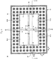
- Fig. 1 is a plan view of a semiconductor device according to a first embodiment of the invention
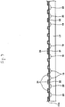
- Fig. 2 is a sectional view in a direction of line A-A of the semiconductor device shown in Fig. 1 .
- B shows a region (hereinafter called "a mounting region B") on a substrate 13 on which semiconductor chips 11-1, 11-2, 12-1, 12-2 are mounted. Also, in Fig.
- H1 shows a height (hereinafter called “a height H1") of the semiconductor chips 11-1, 11-2, 12-1, 12-2 in the case of using a surface 17A of a base material 17 as the reference and H2 shows a height (hereinafter called “a height H2") of external connection terminals 27 in the case of using the surface 17A of the base material 17 as the reference, respectively.
- a semiconductor device 10 has plural semiconductor chips 11-1, 11-2, 12-1, 12-2 (four chips in the present embodiment) and the substrate 13.
- the semiconductor chips 11-1, 11-2 are semiconductor chips with functions different from those of the semiconductor chips 12-1, 12-2.
- a semiconductor chip for memory can be used and in that case, as semiconductor chips 12-1, 12-2, for example, a semiconductor chip for ASIC can be used.
- a semiconductor substrate of the semiconductor chips 11-1, 11-2, 12-1, 12-2, for example, a silicon substrate can be used as a semiconductor substrate of the semiconductor chips 11-1, 11-2, 12-1, 12-2, for example.
- a silicon substrate can be used as the semiconductor substrate of the semiconductor chips 11-1, 11-2, 12-1, 12-2.
- Flip chip connection between the semiconductor chips 11-1, 11-2, 12-1, 12-2 and the substrate 13 is made through solder bumps 15 in a state that the semiconductor chips 11-1, 11-2, 12-1, 12-2 are in a mutually close state.
- a distance a (value indicating the extent of proximity) between the semiconductor chips 11-1, 11-2, 12-1, 12-2 can be set at, for example, 50 ⁇ m to 100 ⁇ m.
- a height of the semiconductor device 10 can be decreased as compared with the case of making wire bonding connection.
- An under fill resin 16 is disposed between the semiconductor chips 11-1, 11-2, 12-1, 12-2 and the substrate 13.
- the under fill resin 16 is means for reducing a difference between the semiconductor chips 11-1, 11-2, 12-1, 12-2 and the substrate 13 in a thermal expansion coefficient.
- an epoxy resin can be used as the under fill resin 16.
- the substrate 13 has a base material 17, connection pads 19, 20, wirings 21, 22, a protective film 24, an adhesion layer 25 and the external connection terminals 27.
- the base material 17 is formed in plate shape. Silicon is preferable as material of the base material 17. A difference between the substrate 13 and the semiconductor chips 11-1, 11-2, 12-1, 12-2 comprising a silicon substrate in a thermal expansion coefficient can be reduced by using silicon as material of the base material 17.
- connection pads 19, 20 and the wirings 21, 22 are respectively disposed on the surface 17A of the base material 17.
- the connection pads 19 are disposed on the base material 17 so as to correspond to the mounting region B of the semiconductor chips 11-1, 11-2, 12-1, 12-2.
- the connection pads 19 are electrically connected to the semiconductor chips 11-1, 11-2, 12-1, 12-2 through the solder bumps 15.
- connection pads 20 are disposed on the base material 17 so as to surround the mounting region B of the semiconductor chips 11-1, 11-2, 12-1, 12-2.
- the connection pads 20 are means for arranging the external connection terminals 27, and are electrically connected to the external connection terminals 27 through the adhesion layer 25.
- the wiring 21 is disposed in the vicinity of the center of the base material 17.
- the wiring 21 makes electrical connection between the connection pads 19 connected to the semiconductor chip 11-1 and the connection pads 19 connected to the semiconductor chip 11-2. Electrical connection between the semiconductor chips 11-1, 11-2 is made by this wiring 21. Also, electrical connection between the connection pads 19 connected to the semiconductor chip 12-1 and the connection pads 19 connected to the semiconductor chip 12-2 is made by the wiring 21 (not shown).
- the wiring 22 makes electrical connection between the connection pads 19 and the connection pad 20. Electrical connection between the external connection terminals 27 and each of the semiconductor chips 11-1, 11-2, 12-1, 12-2 is made by this wiring 22.
- a conductive material can be used and concretely, A1 can be used.
- the protective film 24 is disposed so as to cover the wirings 21, 22 and the surface 17A of the base material 17 with the connection pads 19, 20 exposed.
- material of the protective film 24 for example, a polyimide resin can be used.
- the adhesion layer 25 is disposed on the connection pads 19, 20.
- the adhesion layer 25 disposed on the connection pads 19 is means for improving properties of adhesion between the connection pads 19 and the solder bumps 15.
- the adhesion layer 25 disposed on the connection pads 20 is means for improving properties of adhesion between the connection pads 20 and the external connection terminals 27.
- the external connection terminals 27 are columnar conductive members protruding beyond the semiconductor chips 11-1, 11-2, 12-1, 12-2, and are disposed on the connection pads 20 on which the adhesion layer 25 is formed.
- the external connection terminals 27 are electrically connected to the semiconductor chips 11-1, 11-2, 12-1, 12-2 through the connection pads 20.
- the height H2 of the external connection terminal 27 is set so as to become higher than the height H1 of the semiconductor chips 11-1, 11-2, 12-1, 12-2 (H2>H1).
- the external connection terminal 27 is a terminal for making connection to a mounting substrate such as a motherboard (not shown).
- connection portions 27A portions electrically connected to a mounting substrate etc. of the external connection terminals 27 are prevented from being covered with the under fill resin 16, so that reliability of electrical connection between the semiconductor device 10 and a mounting substrate (not shown) can be improved.
- the external connection terminals 27 can be disposed closer to the semiconductor chips 11-1, 11-2, 12-1, 12-2 than ever before, so that a size (area) of the substrate 13 is decreased and the semiconductor device 10 can be miniaturized.
- a part of the external connection terminal 27 located in the side of the base material 17 is covered with the under fill resin 16.
- the external connection terminal 27 can be reinforced.
- a position of the external connection terminal 27 on the substrate 13 can be regulated by this reinforcement.
- the height H2 of the external connection terminal 27 can be set at 200 ⁇ m.
- a diameter R1 of the external connection terminal 27 can be set at, for example, 200 ⁇ m and in this case, an arrangement pitch P of the external connection terminals 27 can be set at, for example, 400 ⁇ m.
- a distance b between each of the semiconductor chips 11-1, 11-2, 12-1, 12-2 and the external connection terminal 27 closest to each of the semiconductor chips 11-1, 11-2, 12-1, 12-2 can be set at, for example, 50 ⁇ m to 300 ⁇ m, preferably, 50 ⁇ m.
- material of the external connection terminal 27 a conductive material can be used and concretely, Cu can be used.
- the semiconductor device of the embodiment by disposing the external connection terminals 27 protruding beyond the semiconductor chips 11-1, 11-2, 12-1, 12-2 on the surface 17A of the base material 17 to which plural semiconductor chips 11-1, 11-2, 12-1, 12-2 with different functions are connected, the connection portions 27A of the external connection terminals 27 are prevented from being covered with the under fill resin 16, so that the external connection terminals 27 are placed closer to the semiconductor chips 11-1, 11-2, 12-1, 12-2 than ever before and a size (area) of the substrate 13 is decreased and the semiconductor device 10 can be miniaturized.
- Figs. 3 to 9 are diagrams showing manufacturing steps of the semiconductor device according to the first embodiment.
- the same numerals are assigned to the same components as those of the semiconductor device 10 described above.
- connection pads 19, 20 and wirings 21, 22 are simultaneously formed on a surface 17A of a base material 17.
- a protective film 24 is formed so as to cover the wirings 21, 22 and the surface 17A of the base material 17 with the connection pads 19, 20 exposed.
- a silicon wafer having plural substrate formation regions (regions in which a substrate 13 is formed) is used as the base material 17 and an A1 film is formed on the surface 17A of the base material 17 by a sputtering method and thereafter, a resist layer patterned is formed on the A1 film and subsequently, the A1 film is etched by a dry etching method using the resist layer as a mask and the connection pads 19, 20 and the wirings 21, 22 are simultaneously formed.
- the protective film 24 is formed by, for example, applying a polyimide resin by a screen printing method.
- the A1 film may be formed using a vapor deposition method or a CVD method other than the sputtering method.
- an adhesion layer 25 is formed so as to cover an upper surface of the structure shown in Fig. 3 .
- the adhesion layer 25 for example, a Ti/Cu laminated film in which a Ti film and a Cu film are sequentially laminated by a sputtering method can be used.
- the adhesion layer 25 may be formed by a vapor deposition method or a CVD method, etc. other than the sputtering method.
- a resist layer 29 having openings 29A is formed on the structure shown in Fig. 4 .
- the openings 29A are openings for exposing the adhesion layer 25 formed on the connection pads 20.
- external connection terminals 27 are formed by precipitating a conductive metal film on the adhesion layer 25 exposed to the openings 29A by an electrolytic plating method using the adhesion layer 25 as a power feeding layer.
- a conductive metal film for example, a Cu film can be used.
- a height H2 of the external connection terminal 27 can be set at, for example, 200 ⁇ m.
- a diameter R1 of the external connection terminal 27 can be set at, for example, 200 ⁇ m and in this case, an arrangement pitch P of the external connection terminals 27 can be set at, for example, 400 ⁇ m.
- solder bump 15 is a bump in which solder disposed on each of the semiconductor chips 11-1, 11-2, 12-1, 12-2 and solder disposed on the adhesion layer 25 corresponding to the connection pads 19 are melted.
- a height H1 of the semiconductor chips 11-1, 11-2, 12-1, 12-2 can be set at, for example, 70 ⁇ m.
- an under fill resin 16 is filled between the semiconductor chips 11-1, 11-2, 12-1, 12-2 and the substrate 13 and also covers parts of the external connection terminals 27.
- the under fill resin 16 for example, an epoxy resin can be used.
- the semiconductor device 10 further may be sealed by a sealing resin with the surface 17A of the base material 17 exposed.
- a sealing resin with the surface 17A of the base material 17 exposed.
- the semiconductor device 10 is easy to be handled.
- a thermal expansion coefficient difference between the whole of the semiconductor device 10 and a mounting substrate (mounting substrate 61 in Fig. 16 ) of an electronic apparatus can be reduced since the whole thermal expansion coefficient of the semiconductor device 10 sealed by the sealing resin is increased in comparison with the thermal expansion coefficient of the semiconductor device which is not sealed.
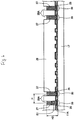
- Fig. 10 is a sectional view of a semiconductor device according to a modified example of the embodiment.
- the description is omitted by assigning the same numerals to the same components as those of the semiconductor device 10 described in Figs. 2 and 3 .
- a semiconductor device 45 has semiconductor chips 11-1, 11-2, 12-1, 12-2 and a substrate 46.
- the substrate 46 is configured in a manner similar to the substrate 13 except that conductive members 47 are further disposed in the configuration of the substrate 13 described above.
- the conductive members 47 are disposed on an adhesion layer 25 formed on connection pads 19.
- the conductive members 47 are electrically connected to the semiconductor chips 11-1, 11-2, 12-1, 12-2 through solder 48.
- a thickness of the conductive member 47 can be set at, for example, 15 ⁇ m to 20 ⁇ m.
- material of the conductive member 47 material having good adhesion to the solder is preferable and, for example, Cu can be used.
- the conductive members 47 By disposing the conductive members 47 on the adhesion layer 25 formed on the connection pads 19 thus, the amount of solder necessary in the case of connecting the semiconductor chips 11-1, 11-2, 12-1, 12-2 to the substrate 46 is decreased and manufacturing cost of the semiconductor device 45 can be reduced.
- Figs. 11 to 15 are diagrams showing manufacturing steps of the semiconductor device according to the modified example of the embodiment.
- the same numerals are assigned to the same components as those of the semiconductor device 45 described above.
- a manufacturing method of the semiconductor device 45 according to the modified example of the embodiment will be described with reference to Figs. 11 to 15 .
- the structure shown in Fig. 4 is formed by the steps of Figs. 4 and 5 described above.
- a resist layer 51 having openings 51A, 51B is formed on the structure shown in Fig. 4 .
- the openings 51A correspond to formation positions of conductive members 47, and an adhesion layer 25 formed on connection pads 19 is exposed.
- the openings 51B correspond to formation positions of external connection terminals 27, and the adhesion layer 25 formed on connection pads 20 is exposed.
- the conductive members 47 are formed in the openings 51A by precipitating a conductive metal film 52 on the adhesion layer 25 exposed to the openings 51A, 51B by an electrolytic plating method using the adhesion layer 25 as a power feeding layer.
- a conductive metal film 52 for example, a Cu film can be used.
- a thickness of the conductive metal film 52 can be set at, for example, 15 ⁇ m to 20 ⁇ m
- the resist layer 51 is removed after the conductive members 47 are formed.
- the conductive metal film 52 formed on the adhesion layer 25 corresponding to the openings 51A is illustrated as the conductive members 47.
- a resist layer 53 having openings 53A for exposing the conductive metal film 52 disposed over the connection pads 20 is formed and subsequently, a conductive metal film 54 is formed on the conductive metal film 52 by an electrolytic plating method using the conductive metal film 52 exposed from the openings 53A as a power feeding layer.
- the external connection terminals 27 made of the conductive metal film 52 and the conductive metal film 54 are formed.
- a height H2 of the external connection terminal 27 using a surface 17A of a base material 17 as the reference can be set at, for example, 200 ⁇ m.
- solder 48 is disposed on electrode pads (not shown) of the semiconductor chips 11-1, 11-2, 12-1, 12-2 and this solder 48 is electrically connected to the conductive members 47.
- the solder 48 is disposed on only the semiconductor chips 11-1, 11-2, 12-1, 12-2 and the semiconductor chips 11-1, 11-2, 12-1, 12-2 can be connected to the substrate 46, so that the amount of solder necessary for connection is decreased and manufacturing cost of the semiconductor device 45 can be reduced.
- the substrate 46 to which the semiconductor chips 11-1, 11-2, 12-1, 12-2 are connected is diced by dicing. Thereafter, the semiconductor device 45 is manufactured by performing processing similar to the step of Fig. 9 described above.
- Fig. 16 is a sectional view of an electronic apparatus comprising a semiconductor device of the embodiment.
- the same numerals are assigned to the same components as those of the semiconductor device 10 described above.
- an electronic apparatus 60 has a semiconductor device 10 and a mounting substrate 61.
- the mounting substrate 61 has connection pads 62 (first connection pads) and external connection terminals 63.
- connection pads 62 are disposed on an upper surface 61A of the mounting substrate 61 and are placed as opposed to external connection terminals 27 of the semiconductor device 10.
- the connection pads 62 are electrically connected to the external connection terminals 27 of the semiconductor device 10 through solder 65. Also, the connection pads 62 are electrically connected to the external connection terminals 63 by a wiring pattern (not shown).
- a motherboard can be used as the mounting substrate 61.
- connection pads 62 are placed inside the mounting substrate 61 than ever before and a size (area) of the mounting substrate 61 is decreased and the electronic apparatus 60 can be miniaturized.
- the need for the sealing resin 115 which was required in the related-art electronic apparatus 100 for making wire bonding connection between the semiconductor device 101 and the mounting substrate 102 is eliminated, so that manufacturing cost of the electronic apparatus 60 can be reduced and also a height of the electronic apparatus 60 can be decreased.
- the electronic apparatus 60 comprising the semiconductor device 10 and the mounting substrate 61 has been described as an example, but effect similar to that of the electronic apparatus 60 can also be obtained in an electronic apparatus in which a semiconductor 45 is disposed instead of the semiconductor device 10.
- Fig. 17 is a sectional view of a semiconductor device according to a second embodiment of the invention.
- the same numerals are assigned to the same components as those of the semiconductor device 10 described in the first embodiment.
- a semiconductor device 70 is configured in a manner similar to the semiconductor device 10 described above except that metal layers 71 are disposed on semiconductor chips 11-1, 11-2, 12-1, 12-2.
- the metal layers 71 are disposed on surfaces of the semiconductor chips 11-1, 11-2, 12-1, 12-2 opposite to the side connected to a substrate 13.
- a Ti/Au laminated film in which a Ti film and an Au film are sequentially laminated can be used.
- effect similar to that of the semiconductor device 10 of the first embodiment can also be obtained in the semiconductor device 70 of the present embodiment.
- Fig. 18 is a sectional view of an electronic apparatus comprising a semiconductor device of the embodiment.
- the same numerals are assigned to the same components as those of the electronic apparatus 60 described in the first embodiment.
- an electronic apparatus 75 has a semiconductor device 70 and a mounting substrate 76.
- the mounting substrate 76 is configured in a manner similar to the mounting substrate 61 described in the first embodiment except that connection pads 78 (second connection pads) are further disposed.
- the connection pads 78 are placed as opposed to the metal layers 71 disposed on the semiconductor chips 11-1, 11-2, 12-1, 12-2.
- the connection pads 78 are electrically connected to the metal layers 71 through solder 79.
- connection pads 78 by disposing the connection pads 78 on the mounting substrate 76 and electrically connecting the connection pads 78 to the metal layers 71 disposed on the semiconductor chips 11-1, 11-2, 12-1, 12-2 through the solder 79, heat generated in the semiconductor chips 11-1, 11-2, 12-1, 12-2 can be radiated efficiently.
- similar effect can also be obtained using a semiconductor device in which the metal layers 71 are disposed on the semiconductor chips 11-1, 11-2, 12-1, 12-2 of the semiconductor device 45 described in Fig. 10 instead of the semiconductor device 70.
- effect similar to that of the electronic apparatus 60 described in the first embodiment can also be obtained in the electronic apparatus 75 of the embodiment.
- the invention can be applied to a semiconductor device and an electronic apparatus capable of achieving miniaturization and improving reliability of electrical connection between the semiconductor device and a mounting substrate.
Landscapes
- Wire Bonding (AREA)
- Structures Or Materials For Encapsulating Or Coating Semiconductor Devices Or Solid State Devices (AREA)
Description
- The present disclosure relates to a semiconductor device and an electronic apparatus, and particularly to a semiconductor device in which plural semiconductor chips are connected on the same substrate, and an electronic apparatus.
- In the related art, system LSI in which memory or an ASIC, etc. are mixed and installed in one semiconductor chip has been developed as miniaturization of a semiconductor device in which a semiconductor chip is installed on a substrate. However, there were problems that the system LSI requires time in a development period or an increase in manufacturing cost.
- Therefore, there is a semiconductor device for achieving miniaturization by closely connecting plural semiconductor chips (for example, memory or an ASIC) with different functions on the same substrate (see
Fig. 19 ). -
Fig. 19 is a sectional view of an electronic apparatus comprising a semiconductor device in which plural semiconductor chips with different functions are closely connected on the same substrate. - An
electronic apparatus 100 has asemiconductor device 101, amounting substrate 102 and asealing resin 115 as shown inFig. 19 . Thesemiconductor device 101 has asubstrate 103 andsemiconductor chips - The
substrate 103 has abase material 105,connection pads wirings protective film 109. Theconnection pads wirings upper surface 105A of thebase material 105. Theconnection pads 106 are electrically connected to thesemiconductor chips connection pads 107 are electrically connected to themounting substrate 102. - The
wiring 108 makes electrical connection between theconnection pads 106 located in the vicinity of the center of thebase material 105. Thewiring 116 makes electrical connection between theconnection pads 106 and theconnection pads 107. Theprotective film 109 is disposed so as to cover thewirings connection pads - The
semiconductor chips semiconductor chips connection pads 106 disposed on thesubstrate 103. Anunder fill resin 110 for reducing a difference in a thermal expansion coefficient is disposed between thesemiconductor chips substrate 103. - The
semiconductor device 101 configured as described above is attached to themounting substrate 102 by an adhesive 111. Also, theconnection pads 107 andconnection pads 113 disposed on themounting substrate 102 are connected by wires 114 (wire bonding connection). Also, thesemiconductor device 101 connected by wire bonding is sealed by the sealingresin 115 for protecting the wires 114 (for example, see Japanese Patent Unexamined Publication No.2005-39161 - However, in the related-
art semiconductor device 101, there was a problem that theconnection pads 107 are covered with the under fillresin 110 and electrical connection between thesemiconductor device 101 and themounting substrate 102 cannot be made. - Also, when the
connection pads 107 are placed in a position separated from thesemiconductor chips connection pads 107 are not covered with theunder fill resin 110, there was a problem that a size (area) of thesubstrate 103 increases and thesemiconductor device 101 cannot be miniaturized. - Further, it is necessary to dispose the
connection pads 113 in a position separated from theconnection pads 107 so that thewires 114 can be placed in order to electrically connect theconnection pads 107 to theconnection pads 113 by thewires 114. As a result of that, there was a problem that a size (area) of themounting substrate 102 increases and theelectronic apparatus 100 cannot be miniaturized. - Also, when heights of the
wires 114 are higher than those of thesemiconductor chips wires 114 protrude from thesemiconductor chips sealing resin 115 becomes thick, so that there was a problem that a height H of theelectronic apparatus 100 increases and theelectronic apparatus 100 cannot be miniaturized. -
US 2004/0043534 A1 discloses a semiconductor device which includes a first semiconductor chip, a substrate onto which the first semiconductor chip is flip-chip bonded and on which a concave is formed along one side of the first semiconductor chip which is flip-chip bonded, a second semiconductor chip which is flip-chip bonded onto a portion on the substrate opposite the first semiconductor chip across the concave on the substrate, and a resin applied to spaces between the substrate and the first and second semiconductor chips. -
US 2004/0053442 A1 concerns a semiconductor package comprising multiple stacked substrates having flip chips attached to the substrates with chip-on-board assembly techniques to achieve dense packaging. The substrates are preferably stacked atop one another by electric connections which are column-like structures. The electric connections achieve electric communication between the stacked substrates, must be of sufficient height to give clearance for the components mounted on the substrates, and should preferably be sufficiently strong to give support between the stacked substrates. -
US 2003/0227066 A1 discloses an apparatus and methods, wherein the reflowable electrically conductive interconnect material coupling the interconnects and/or land-side components of a microelectronic package is protected from elevated temperatures, such as those associated with reflow processes and environments which exceed the melting temperature of the interconnect material. One embodiment of the method provides covering the interconnect material about the interconnects and/or land-side components with heat-resistant curable material which protects the interconnect material from the elevated temperature and provides structural support to the interconnects and/or land-side components at the elevated temperature. -
EP 1 067 603 A2 -
EP 1 137 067 A2 -
JP 2002-368027 A - The present invention intends to imrpove at least some of the above problems. The object is solved by the semiconductor device according to
independent claim 1 and by the electronic apparatus according to claim 5. - Further advantages, features, aspects and details of the invention are evident from the dependent claims, the description and the drawings.
- Embodiments of the present invention provide a semiconductor device and an electronic apparatus capable of achieving miniaturization and improving reliability of electrical connection between the semiconductor device and a mounting substrate.
- According to one aspect of one or more embodiments of the invention, there is provided a semiconductor device according to
claim 1. - According to the invention, by disposing an external connection terminal on a substrate of the side to which plural semiconductor chips are connected and also protruding the external connection terminal beyond the plural semiconductor chips, for example, when an under fill resin is disposed between the plural semiconductor chips and the substrate, a connection portion (portion electrically connected to a mounting substrate etc.) of the external connection terminal is prevented from being covered with the under fill resin, so that reliability of electrical connection to a semiconductor device can be improved. Also, the external connection terminal is placed closer to the plural semiconductor chips than ever before and an area of the substrate is decreased and the semiconductor device can be miniaturized.
- Also, an under fill resin is disposed between the plural semiconductor chips and the substrate, and a part of the external connection terminal located in the side of the substrate is covered with the under fill resin. By covering a part of the external connection terminal located in the side of the substrate with the under fill resin thus, the external connection terminal can be reinforced.
- Further, the plural semiconductor chips may be semiconductor chips with different functions and may be placed mutually closely. By mutually closely placing the plural semiconductor chips with different functions thus, the plural semiconductor chips can achieve a function near to system LSI.
- According to another aspect of one or more embodiments of the invention, there is provided an electronic apparatus comprising a semiconductor device as claimed in any one of claims 1-3, and a mounting substrate having a first connection pad opposed to the external connection terminal, and wherein the external connection terminal is electrically connected to the first connection pad.
- According to the invention, by disposing a first connection pad on a mounting substrate as opposed to an external connection terminal, an area of the mounting substrate is decreased and an electronic apparatus can be miniaturized. Also, the need for a sealing resin which was required in the related-art electronic apparatus for making wire bonding connection between the semiconductor device and the mounting substrate is eliminated, so that a height of the electronic apparatus can be decreased. Further, the need for the sealing resin is eliminated, so that manufacturing cost of the electronic apparatus can be reduced.
- Further, the mounting substrate further has a second connection pad, and the plural semiconductor chips comprise a metal layer on a surface opposite to a surface to which the substrate is connected, and the second connection pad may be electrically connected to the metal layer. As a result of this, heat accumulated in the plural semiconductor chips can be radiated efficiently.
- Various implementations may include one or more the following advantages. For example, a semiconductor device and an electronic apparatus capable of achieving miniaturization and improving reliability of electrical connection between the semiconductor device and a mounting substrate can be provided.
- The disclosure is also directed to apparatuses for carrying out the disclosed methods and including apparatus parts for performing each described method steps. These method steps may be performed by way of hardware components, a computer programmed by appropriate software, by any combination of the two or in any other manner. Furthermore, the invention is also directed to methods by which the described apparatus operates or is manufactured. It includes method steps for carrying out every function of the apparatus or manufacturing every part of the apparatus.
- Other features and advantages may be apparent from the following detailed description, the accompanying drawings and the claims.
-
-
Fig. 1 is a plan view of a semiconductor device according to a first embodiment of the invention. -
Fig. 2 is a sectional view in a direction of line A-A of the semiconductor device shown inFig. 1 . -
Fig. 3 is a diagram showing a manufacturing step of the semiconductor device according to the first embodiment (first). -
Fig. 4 is a diagram showing a manufacturing step of the semiconductor device according to the first embodiment (second). -
Fig. 5 is a diagram showing a manufacturing step of the semiconductor device according to the first embodiment (third). -
Fig. 6 is a diagram showing a manufacturing step of the semiconductor device according to the first embodiment (fourth). -
Fig. 7 is a diagram showing a manufacturing step of the semiconductor device according to the first embodiment (fifth). -
Fig. 8 is a diagram showing a manufacturing step of the semiconductor device according to the first embodiment (sixth). -
Fig. 9 is a diagram showing a manufacturing step of the semiconductor device according to the first embodiment (seventh). -
Fig. 10 is a sectional view of a semiconductor device according to a modified example of the embodiment. -
Fig. 11 is a diagram showing a manufacturing step of the semiconductor device according to the modified example of the embodiment (first). -
Fig. 12 is a diagram showing a manufacturing step of the semiconductor device according to the modified example of the embodiment (second). -
Fig. 13 is a diagram showing a manufacturing step of the semiconductor device according to the modified example of the embodiment (third). -
Fig. 14 is a diagram showing a manufacturing step of the semiconductor device according to the modified example of the embodiment (fourth). -
Fig. 15 is a diagram showing a manufacturing step of the semiconductor device according to the modified example of the embodiment (fifth). -
Fig. 16 is a sectional view of an electronic apparatus comprising a semiconductor device of the first embodiment. -
Fig. 17 is a sectional view of a semiconductor device according to a second embodiment of the invention. -
Fig. 18 is a sectional view of an electronic apparatus comprising a semiconductor device of the second embodiment. -
Fig. 19 is a sectional view of an electronic apparatus comprising a semiconductor device in which plural semiconductor chips with different functions are closely connected on the same substrate. - Next, embodiments of the invention will be described based on the drawings.
-
Fig. 1 is a plan view of a semiconductor device according to a first embodiment of the invention, andFig. 2 is a sectional view in a direction of line A-A of the semiconductor device shown inFig. 1 . InFig. 1 , B shows a region (hereinafter called "a mounting region B") on asubstrate 13 on which semiconductor chips 11-1, 11-2, 12-1, 12-2 are mounted. Also, inFig. 2 , H1 shows a height (hereinafter called "a height H1") of the semiconductor chips 11-1, 11-2, 12-1, 12-2 in the case of using asurface 17A of abase material 17 as the reference and H2 shows a height (hereinafter called "a height H2") ofexternal connection terminals 27 in the case of using thesurface 17A of thebase material 17 as the reference, respectively. - Referring to
Figs. 1 and2 , asemiconductor device 10 has plural semiconductor chips 11-1, 11-2, 12-1, 12-2 (four chips in the present embodiment) and thesubstrate 13. - The semiconductor chips 11-1, 11-2 are semiconductor chips with functions different from those of the semiconductor chips 12-1, 12-2. As the semiconductor chips 11-1, 11-2, for example, a semiconductor chip for memory can be used and in that case, as semiconductor chips 12-1, 12-2, for example, a semiconductor chip for ASIC can be used. Also, as a semiconductor substrate of the semiconductor chips 11-1, 11-2, 12-1, 12-2, for example, a silicon substrate can be used. The case of using the silicon substrate as the semiconductor substrate of the semiconductor chips 11-1, 11-2, 12-1, 12-2 will be described below as an example.
- Flip chip connection between the semiconductor chips 11-1, 11-2, 12-1, 12-2 and the
substrate 13 is made through solder bumps 15 in a state that the semiconductor chips 11-1, 11-2, 12-1, 12-2 are in a mutually close state. - By connecting the semiconductor chips 11-1, 11-2, 12-1, 12-2 to the
substrate 13 in the state that the semiconductor chips 11-1, 11-2, 12-1, 12-2 are in the close state thus, the semiconductor chips 11-1, 11-2, 12-1, 12-2 can achieve a function near to system LSI. A distance a (value indicating the extent of proximity) between the semiconductor chips 11-1, 11-2, 12-1, 12-2 can be set at, for example, 50 µm to 100 µm. - Also, by making flip chip connection of the semiconductor chips 11-1, 11-2, 12-1, 12-2, a height of the
semiconductor device 10 can be decreased as compared with the case of making wire bonding connection. - An under
fill resin 16 is disposed between the semiconductor chips 11-1, 11-2, 12-1, 12-2 and thesubstrate 13. The under fillresin 16 is means for reducing a difference between the semiconductor chips 11-1, 11-2, 12-1, 12-2 and thesubstrate 13 in a thermal expansion coefficient. As the under fillresin 16, for example, an epoxy resin can be used. - The
substrate 13 has abase material 17,connection pads protective film 24, anadhesion layer 25 and theexternal connection terminals 27. Thebase material 17 is formed in plate shape. Silicon is preferable as material of thebase material 17. A difference between thesubstrate 13 and the semiconductor chips 11-1, 11-2, 12-1, 12-2 comprising a silicon substrate in a thermal expansion coefficient can be reduced by using silicon as material of thebase material 17. - A plurality of the
connection pads wirings surface 17A of thebase material 17. Theconnection pads 19 are disposed on thebase material 17 so as to correspond to the mounting region B of the semiconductor chips 11-1, 11-2, 12-1, 12-2. Theconnection pads 19 are electrically connected to the semiconductor chips 11-1, 11-2, 12-1, 12-2 through the solder bumps 15. - The
connection pads 20 are disposed on thebase material 17 so as to surround the mounting region B of the semiconductor chips 11-1, 11-2, 12-1, 12-2. Theconnection pads 20 are means for arranging theexternal connection terminals 27, and are electrically connected to theexternal connection terminals 27 through theadhesion layer 25. - The
wiring 21 is disposed in the vicinity of the center of thebase material 17. Thewiring 21 makes electrical connection between theconnection pads 19 connected to the semiconductor chip 11-1 and theconnection pads 19 connected to the semiconductor chip 11-2. Electrical connection between the semiconductor chips 11-1, 11-2 is made by thiswiring 21. Also, electrical connection between theconnection pads 19 connected to the semiconductor chip 12-1 and theconnection pads 19 connected to the semiconductor chip 12-2 is made by the wiring 21 (not shown). - The
wiring 22 makes electrical connection between theconnection pads 19 and theconnection pad 20. Electrical connection between theexternal connection terminals 27 and each of the semiconductor chips 11-1, 11-2, 12-1, 12-2 is made by thiswiring 22. As material of theconnection pads wirings - The
protective film 24 is disposed so as to cover thewirings surface 17A of thebase material 17 with theconnection pads protective film 24, for example, a polyimide resin can be used. - The
adhesion layer 25 is disposed on theconnection pads adhesion layer 25 disposed on theconnection pads 19 is means for improving properties of adhesion between theconnection pads 19 and the solder bumps 15. Also, theadhesion layer 25 disposed on theconnection pads 20 is means for improving properties of adhesion between theconnection pads 20 and theexternal connection terminals 27. As theadhesion layer 25, for example, a Ti/Cu laminated film in which a Ti film and a Cu film are sequentially laminated from the side of theconnection pads - The
external connection terminals 27 are columnar conductive members protruding beyond the semiconductor chips 11-1, 11-2, 12-1, 12-2, and are disposed on theconnection pads 20 on which theadhesion layer 25 is formed. Theexternal connection terminals 27 are electrically connected to the semiconductor chips 11-1, 11-2, 12-1, 12-2 through theconnection pads 20. - The height H2 of the
external connection terminal 27 is set so as to become higher than the height H1 of the semiconductor chips 11-1, 11-2, 12-1, 12-2 (H2>H1). Theexternal connection terminal 27 is a terminal for making connection to a mounting substrate such as a motherboard (not shown). - By disposing the
external connection terminals 27 protruding beyond the semiconductor chips 11-1, 11-2, 12-1, 12-2 on thesurface 17A of thebase material 17 to which plural semiconductor chips 11-1, 11-2, 12-1, 12-2 are connected thus,connection portions 27A (portions electrically connected to a mounting substrate etc.) of theexternal connection terminals 27 are prevented from being covered with theunder fill resin 16, so that reliability of electrical connection between thesemiconductor device 10 and a mounting substrate (not shown) can be improved. - Also, the
external connection terminals 27 can be disposed closer to the semiconductor chips 11-1, 11-2, 12-1, 12-2 than ever before, so that a size (area) of thesubstrate 13 is decreased and thesemiconductor device 10 can be miniaturized. - Also, a part of the
external connection terminal 27 located in the side of thebase material 17 is covered with theunder fill resin 16. By covering a part of theexternal connection terminal 27 with theunder fill resin 16 thus, theexternal connection terminal 27 can be reinforced. Also, a position of theexternal connection terminal 27 on thesubstrate 13 can be regulated by this reinforcement. - For example, when the height H1 of the semiconductor chips 11-1, 11-2, 12-1, 12-2 is 70 µm, the height H2 of the
external connection terminal 27 can be set at 200 µm. Also, a diameter R1 of theexternal connection terminal 27 can be set at, for example, 200 µm and in this case, an arrangement pitch P of theexternal connection terminals 27 can be set at, for example, 400 µm. A distance b between each of the semiconductor chips 11-1, 11-2, 12-1, 12-2 and theexternal connection terminal 27 closest to each of the semiconductor chips 11-1, 11-2, 12-1, 12-2 can be set at, for example, 50 µm to 300 µm, preferably, 50 µm. As material of theexternal connection terminal 27, a conductive material can be used and concretely, Cu can be used. - According to the semiconductor device of the embodiment, by disposing the
external connection terminals 27 protruding beyond the semiconductor chips 11-1, 11-2, 12-1, 12-2 on thesurface 17A of thebase material 17 to which plural semiconductor chips 11-1, 11-2, 12-1, 12-2 with different functions are connected, theconnection portions 27A of theexternal connection terminals 27 are prevented from being covered with theunder fill resin 16, so that theexternal connection terminals 27 are placed closer to the semiconductor chips 11-1, 11-2, 12-1, 12-2 than ever before and a size (area) of thesubstrate 13 is decreased and thesemiconductor device 10 can be miniaturized. -
Figs. 3 to 9 are diagrams showing manufacturing steps of the semiconductor device according to the first embodiment. InFigs. 3 to 9 , the same numerals are assigned to the same components as those of thesemiconductor device 10 described above. - A manufacturing method of the semiconductor device according to the first embodiment will be described with reference to
Figs. 3 to 9 . First, in a step ofFig. 3 ,connection pads wirings surface 17A of abase material 17. Next, aprotective film 24 is formed so as to cover thewirings surface 17A of thebase material 17 with theconnection pads substrate 13 is formed) is used as thebase material 17 and an A1 film is formed on thesurface 17A of thebase material 17 by a sputtering method and thereafter, a resist layer patterned is formed on the A1 film and subsequently, the A1 film is etched by a dry etching method using the resist layer as a mask and theconnection pads wirings protective film 24 is formed by, for example, applying a polyimide resin by a screen printing method. In addition, the A1 film may be formed using a vapor deposition method or a CVD method other than the sputtering method. - Then, in a step of
Fig. 4 , anadhesion layer 25 is formed so as to cover an upper surface of the structure shown inFig. 3 . As theadhesion layer 25, for example, a Ti/Cu laminated film in which a Ti film and a Cu film are sequentially laminated by a sputtering method can be used. Theadhesion layer 25 may be formed by a vapor deposition method or a CVD method, etc. other than the sputtering method. - Then, in a step of
Fig. 5 , a resistlayer 29 havingopenings 29A is formed on the structure shown inFig. 4 . Theopenings 29A are openings for exposing theadhesion layer 25 formed on theconnection pads 20. - Then, in a step of
Fig. 6 ,external connection terminals 27 are formed by precipitating a conductive metal film on theadhesion layer 25 exposed to theopenings 29A by an electrolytic plating method using theadhesion layer 25 as a power feeding layer. As the conductive metal film, for example, a Cu film can be used. A height H2 of theexternal connection terminal 27 can be set at, for example, 200 µm. Also, a diameter R1 of theexternal connection terminal 27 can be set at, for example, 200 µm and in this case, an arrangement pitch P of theexternal connection terminals 27 can be set at, for example, 400 µm. - Then, in a step of
Fig. 7 , the resistlayer 29 is removed and thereafter, theadhesion layer 25 disposed in the portion other than theconnection pads substrate 13 is formed in each of the substrate formation regions on the silicon wafer. - Then, in a step of
Fig. 8 , semiconductor chips 11-1, 11-2, 12-1, 12-2 are connected through solder bumps 15 on theconnection pads 19 on which theadhesion layer 25 is disposed (flip chip connection). Thesolder bump 15 is a bump in which solder disposed on each of the semiconductor chips 11-1, 11-2, 12-1, 12-2 and solder disposed on theadhesion layer 25 corresponding to theconnection pads 19 are melted. A height H1 of the semiconductor chips 11-1, 11-2, 12-1, 12-2 can be set at, for example, 70 µm. Thereafter, thesubstrate 13 on which the semiconductor chips 11-1, 11-2, 12-1, 12-2 are mounted is diced by dicing. - Then, in a step of
Fig. 9 , an underfill resin 16 is filled between the semiconductor chips 11-1, 11-2, 12-1, 12-2 and thesubstrate 13 and also covers parts of theexternal connection terminals 27. As the under fillresin 16, for example, an epoxy resin can be used. By the manufacturing method described above, thesemiconductor device 10 is manufactured. - In this embodiment, the
semiconductor device 10 further may be sealed by a sealing resin with thesurface 17A of thebase material 17 exposed. By sealing thesemiconductor device 10 with the sealing resin, thesemiconductor device 10 is easy to be handled. Further, a thermal expansion coefficient difference between the whole of thesemiconductor device 10 and a mounting substrate (mountingsubstrate 61 inFig. 16 ) of an electronic apparatus can be reduced since the whole thermal expansion coefficient of thesemiconductor device 10 sealed by the sealing resin is increased in comparison with the thermal expansion coefficient of the semiconductor device which is not sealed. -
Fig. 10 is a sectional view of a semiconductor device according to a modified example of the embodiment. InFig. 10 , the description is omitted by assigning the same numerals to the same components as those of thesemiconductor device 10 described inFigs. 2 and3 . - Referring to
Fig. 10 , asemiconductor device 45 has semiconductor chips 11-1, 11-2, 12-1, 12-2 and asubstrate 46. - The
substrate 46 is configured in a manner similar to thesubstrate 13 except thatconductive members 47 are further disposed in the configuration of thesubstrate 13 described above. Theconductive members 47 are disposed on anadhesion layer 25 formed onconnection pads 19. Theconductive members 47 are electrically connected to the semiconductor chips 11-1, 11-2, 12-1, 12-2 throughsolder 48. A thickness of theconductive member 47 can be set at, for example, 15 µm to 20 µm. As material of theconductive member 47, material having good adhesion to the solder is preferable and, for example, Cu can be used. - By disposing the
conductive members 47 on theadhesion layer 25 formed on theconnection pads 19 thus, the amount of solder necessary in the case of connecting the semiconductor chips 11-1, 11-2, 12-1, 12-2 to thesubstrate 46 is decreased and manufacturing cost of thesemiconductor device 45 can be reduced. - In addition, effect similar to that of the
semiconductor device 10 described above can also be obtained in thesemiconductor device 45 configured above. -
Figs. 11 to 15 are diagrams showing manufacturing steps of the semiconductor device according to the modified example of the embodiment. InFigs. 11 to 15 , the same numerals are assigned to the same components as those of thesemiconductor device 45 described above. - Next, a manufacturing method of the
semiconductor device 45 according to the modified example of the embodiment will be described with reference toFigs. 11 to 15 . First, the structure shown inFig. 4 is formed by the steps ofFigs. 4 and5 described above. Next, in a step ofFig. 11 , a resistlayer 51 havingopenings Fig. 4 . Theopenings 51A correspond to formation positions ofconductive members 47, and anadhesion layer 25 formed onconnection pads 19 is exposed. Theopenings 51B correspond to formation positions ofexternal connection terminals 27, and theadhesion layer 25 formed onconnection pads 20 is exposed. - Then, in a step of
Fig. 12 , theconductive members 47 are formed in theopenings 51A by precipitating aconductive metal film 52 on theadhesion layer 25 exposed to theopenings adhesion layer 25 as a power feeding layer. As theconductive metal film 52, for example, a Cu film can be used. Also, a thickness of theconductive metal film 52 can be set at, for example, 15 µm to 20 µm The resistlayer 51 is removed after theconductive members 47 are formed. In addition, inFig. 12 , theconductive metal film 52 formed on theadhesion layer 25 corresponding to theopenings 51A is illustrated as theconductive members 47. - Then, in a step of
Fig. 13 , a resistlayer 53 havingopenings 53A for exposing theconductive metal film 52 disposed over theconnection pads 20 is formed and subsequently, aconductive metal film 54 is formed on theconductive metal film 52 by an electrolytic plating method using theconductive metal film 52 exposed from theopenings 53A as a power feeding layer. As a result of this, theexternal connection terminals 27 made of theconductive metal film 52 and theconductive metal film 54 are formed. Also, a height H2 of theexternal connection terminal 27 using asurface 17A of abase material 17 as the reference can be set at, for example, 200 µm. - Then, in a step of
Fig. 14 , the resistlayer 53 is removed and then, theadhesion layer 25 which is not exposed to theconductive members 47 and theexternal connection terminals 27 is removed. Then, in a step ofFig. 15 ,solder 48 is disposed on electrode pads (not shown) of the semiconductor chips 11-1, 11-2, 12-1, 12-2 and thissolder 48 is electrically connected to theconductive members 47. - By forming the
conductive members 47 on theadhesion layer 25 located over theconnection pads 19 thus, thesolder 48 is disposed on only the semiconductor chips 11-1, 11-2, 12-1, 12-2 and the semiconductor chips 11-1, 11-2, 12-1, 12-2 can be connected to thesubstrate 46, so that the amount of solder necessary for connection is decreased and manufacturing cost of thesemiconductor device 45 can be reduced. - Then, the
substrate 46 to which the semiconductor chips 11-1, 11-2, 12-1, 12-2 are connected is diced by dicing. Thereafter, thesemiconductor device 45 is manufactured by performing processing similar to the step ofFig. 9 described above. -
Fig. 16 is a sectional view of an electronic apparatus comprising a semiconductor device of the embodiment. InFig. 16 , the same numerals are assigned to the same components as those of thesemiconductor device 10 described above. - Referring to
Fig. 16 , anelectronic apparatus 60 has asemiconductor device 10 and a mountingsubstrate 61. The mountingsubstrate 61 has connection pads 62 (first connection pads) andexternal connection terminals 63. - The
connection pads 62 are disposed on anupper surface 61A of the mountingsubstrate 61 and are placed as opposed toexternal connection terminals 27 of thesemiconductor device 10. Theconnection pads 62 are electrically connected to theexternal connection terminals 27 of thesemiconductor device 10 throughsolder 65. Also, theconnection pads 62 are electrically connected to theexternal connection terminals 63 by a wiring pattern (not shown). As the mountingsubstrate 61, for example, a motherboard can be used. - According to the electronic apparatus of the embodiment, by disposing the
connection pads 62 on theupper surface 61A of the mountingsubstrate 61 as opposed to theexternal connection terminals 27 of thesemiconductor device 10, theconnection pads 62 are placed inside the mountingsubstrate 61 than ever before and a size (area) of the mountingsubstrate 61 is decreased and theelectronic apparatus 60 can be miniaturized. - Also, by connecting the
external connection terminals 27 of thesemiconductor device 10 to theconnection pads 62 of the mountingsubstrate 61 through thesolder 65, the need for the sealingresin 115 which was required in the related-artelectronic apparatus 100 for making wire bonding connection between thesemiconductor device 101 and the mountingsubstrate 102 is eliminated, so that manufacturing cost of theelectronic apparatus 60 can be reduced and also a height of theelectronic apparatus 60 can be decreased. - In addition, in
Fig. 16 , theelectronic apparatus 60 comprising thesemiconductor device 10 and the mountingsubstrate 61 has been described as an example, but effect similar to that of theelectronic apparatus 60 can also be obtained in an electronic apparatus in which asemiconductor 45 is disposed instead of thesemiconductor device 10. -
Fig. 17 is a sectional view of a semiconductor device according to a second embodiment of the invention. InFig. 17 , the same numerals are assigned to the same components as those of thesemiconductor device 10 described in the first embodiment. - Referring to
Fig. 17 , asemiconductor device 70 is configured in a manner similar to thesemiconductor device 10 described above except that metal layers 71 are disposed on semiconductor chips 11-1, 11-2, 12-1, 12-2. The metal layers 71 are disposed on surfaces of the semiconductor chips 11-1, 11-2, 12-1, 12-2 opposite to the side connected to asubstrate 13. As the metal layers 71, for example, a Ti/Au laminated film in which a Ti film and an Au film are sequentially laminated can be used. In addition, effect similar to that of thesemiconductor device 10 of the first embodiment can also be obtained in thesemiconductor device 70 of the present embodiment. -
Fig. 18 is a sectional view of an electronic apparatus comprising a semiconductor device of the embodiment. InFig. 18 , the same numerals are assigned to the same components as those of theelectronic apparatus 60 described in the first embodiment. - Referring to
Fig. 18 , anelectronic apparatus 75 has asemiconductor device 70 and a mountingsubstrate 76. The mountingsubstrate 76 is configured in a manner similar to the mountingsubstrate 61 described in the first embodiment except that connection pads 78 (second connection pads) are further disposed. Theconnection pads 78 are placed as opposed to the metal layers 71 disposed on the semiconductor chips 11-1, 11-2, 12-1, 12-2. Theconnection pads 78 are electrically connected to the metal layers 71 throughsolder 79. - According to the electronic apparatus of the embodiment, by disposing the
connection pads 78 on the mountingsubstrate 76 and electrically connecting theconnection pads 78 to the metal layers 71 disposed on the semiconductor chips 11-1, 11-2, 12-1, 12-2 through thesolder 79, heat generated in the semiconductor chips 11-1, 11-2, 12-1, 12-2 can be radiated efficiently. Also, in the electronic apparatus of the embodiment, similar effect can also be obtained using a semiconductor device in which the metal layers 71 are disposed on the semiconductor chips 11-1, 11-2, 12-1, 12-2 of thesemiconductor device 45 described inFig. 10 instead of thesemiconductor device 70. In addition, effect similar to that of theelectronic apparatus 60 described in the first embodiment can also be obtained in theelectronic apparatus 75 of the embodiment. - The preferred embodiments of the invention have been described above in detail, but the invention is not limited to such specific embodiments, and various modifications and changes can be made within the scope of the claims.
- The invention can be applied to a semiconductor device and an electronic apparatus capable of achieving miniaturization and improving reliability of electrical connection between the semiconductor device and a mounting substrate.
Claims (6)
- A semiconductor device (10; 45; 70) comprising:a plurality of semiconductor chips (11-1, 11-2, 12-1), each having a front and a back surface; anda substrate having a first and a second surface, an external connection terminal (27) being disposed on the first surface of the substrate (13; 46) and being electrically connected to said plurality of semiconductor chips,wherein the external connection terminal (27) is disposed on the substrate (13; 46) so as to surround the region where the semiconductor chips are mounted, said external connection terminal (27) protruding beyond said plurality of semiconductor chips, wherein
the semiconductor device further comprises a flip chip connection between the front surface of each of the plurality of semiconductor chips (11-1, 11-2, 12-1) and the first surface of the substrate, wherein an underfill resin is disposed between the plurality of semiconductor chips and the substrate (13; 46), and a part of the external connection terminal is covered with the underfill resin, and whereinthe back surface of each semiconductor chip is completely exposed from the underfill resin. - A semiconductor device as claimed in claim 1, wherein the external connection terminal is a columnar conductive member.
- A semiconductor device (10; 45; 70) as claimed in claim 1, wherein conductive members are disposed on the first surface of the substrate and opposed to the plurality of semiconductor chips (11-1, 11-2, 12-1), each of said semiconductor chips having solder disposed thereon, and the flip chip connection being made up by the conductor members and the solder.
- A semiconductor device as in any one of claims 1-3, wherein the plurality of semiconductor chips (11-1, 11-2, 12-1) are semiconductor chips with different functions and are placed mutually closely.
- An electronic apparatus (60; 75) comprising:a semiconductor device (10; 45; 70) as claimed in any one of claims 1-3; anda mounting substrate (61; 76) having a first connection pad opposed to the external connection terminal,wherein the external connection terminal (27) is electrically connected to the first connection pad.
- An electronic apparatus as claimed in claim 5, wherein the mounting substrate further has second connection pads, each semiconductor chip comprising a metal layer on its back surface , and each second connection pad being electrically connected to the metal layer of one of said plurality of semiconductor chips.
Applications Claiming Priority (1)
| Application Number | Priority Date | Filing Date | Title |
|---|---|---|---|
| JP2005206887A JP4498991B2 (en) | 2005-07-15 | 2005-07-15 | Semiconductor device and electronic device |
Publications (3)
| Publication Number | Publication Date |
|---|---|
| EP1744362A2 EP1744362A2 (en) | 2007-01-17 |
| EP1744362A3 EP1744362A3 (en) | 2010-01-20 |
| EP1744362B1 true EP1744362B1 (en) | 2016-12-21 |
Family
ID=37116069
Family Applications (1)
| Application Number | Title | Priority Date | Filing Date |
|---|---|---|---|
| EP06014470.6A Ceased EP1744362B1 (en) | 2005-07-15 | 2006-07-12 | Semiconductor device and electronic apparatus |
Country Status (4)
| Country | Link |
|---|---|
| US (1) | US8169073B2 (en) |
| EP (1) | EP1744362B1 (en) |
| JP (1) | JP4498991B2 (en) |
| KR (1) | KR101214499B1 (en) |
Families Citing this family (10)
| Publication number | Priority date | Publication date | Assignee | Title |
|---|---|---|---|---|
| US8174119B2 (en) * | 2006-11-10 | 2012-05-08 | Stats Chippac, Ltd. | Semiconductor package with embedded die |
| JP2009123763A (en) * | 2007-11-12 | 2009-06-04 | Denso Corp | Semiconductor device and manufacturing method thereof |
| JP4759582B2 (en) * | 2008-02-15 | 2011-08-31 | Okiセミコンダクタ株式会社 | Semiconductor device manufacturing method and semiconductor device |
| JP5854304B2 (en) * | 2011-01-19 | 2016-02-09 | 日立金属株式会社 | Method for producing RTB-based sintered magnet |
| US10971476B2 (en) * | 2014-02-18 | 2021-04-06 | Qualcomm Incorporated | Bottom package with metal post interconnections |
| US9852960B2 (en) * | 2016-03-17 | 2017-12-26 | International Business Machines Corporation | Underfill dispensing using funnels |
| JP2018037465A (en) * | 2016-08-29 | 2018-03-08 | ウシオ電機株式会社 | Semiconductor package and manufacturing method of the same |
| TWI610409B (en) * | 2016-08-30 | 2018-01-01 | Chipmos Technologies Inc. | Semiconductor package and method of manufacturing same |
| CN211858622U (en) | 2017-06-16 | 2020-11-03 | 株式会社村田制作所 | Circuit board and circuit module |
| KR102798789B1 (en) * | 2020-07-09 | 2025-04-22 | 삼성전자주식회사 | Semiconductor package |
Citations (1)
| Publication number | Priority date | Publication date | Assignee | Title |
|---|---|---|---|---|
| JP2002368027A (en) * | 2001-06-06 | 2002-12-20 | Matsushita Electric Ind Co Ltd | Method for manufacturing semiconductor device |
Family Cites Families (15)
| Publication number | Priority date | Publication date | Assignee | Title |
|---|---|---|---|---|
| US4761881A (en) * | 1986-09-15 | 1988-08-09 | International Business Machines Corporation | Single step solder process |
| DE69220333D1 (en) * | 1991-12-11 | 1997-07-17 | Ibm | Electronic assembly with protective encapsulation material |
| JP3110922B2 (en) * | 1993-08-12 | 2000-11-20 | 富士通株式会社 | Multi-chip module |
| JPH10209322A (en) * | 1997-01-22 | 1998-08-07 | Hitachi Ltd | Semiconductor device and its mounting structure |
| US5994166A (en) | 1997-03-10 | 1999-11-30 | Micron Technology, Inc. | Method of constructing stacked packages |
| JP2001024150A (en) | 1999-07-06 | 2001-01-26 | Sony Corp | Semiconductor device |
| JP3823636B2 (en) * | 1999-09-22 | 2006-09-20 | カシオ計算機株式会社 | Semiconductor chip module and manufacturing method thereof |
| US6437990B1 (en) * | 2000-03-20 | 2002-08-20 | Agere Systems Guardian Corp. | Multi-chip ball grid array IC packages |
| JP3768880B2 (en) * | 2001-12-28 | 2006-04-19 | 松下電器産業株式会社 | Flip chip mounting substrate, manufacturing method, and wireless device |
| US6911726B2 (en) * | 2002-06-07 | 2005-06-28 | Intel Corporation | Microelectronic packaging and methods for thermally protecting package interconnects and components |
| JP3639272B2 (en) * | 2002-08-30 | 2005-04-20 | 株式会社東芝 | Semiconductor device and method for manufacturing semiconductor device |
| JP2005039161A (en) | 2003-07-18 | 2005-02-10 | System Fabrication Technologies Inc | Three-dimensional high-density mounting system for semiconductor integrated circuit chips |
| US7732904B2 (en) * | 2003-10-10 | 2010-06-08 | Interconnect Portfolio Llc | Multi-surface contact IC packaging structures and assemblies |
| DE10348620A1 (en) | 2003-10-15 | 2005-06-02 | Infineon Technologies Ag | Semiconductor module with housing contacts |
| KR100441260B1 (en) * | 2003-10-20 | 2004-07-21 | 주식회사 케이이씨 | Rectifier diode package |
-
2005
- 2005-07-15 JP JP2005206887A patent/JP4498991B2/en not_active Expired - Fee Related
-
2006
- 2006-07-12 EP EP06014470.6A patent/EP1744362B1/en not_active Ceased
- 2006-07-12 US US11/457,026 patent/US8169073B2/en active Active
- 2006-07-13 KR KR1020060065646A patent/KR101214499B1/en not_active Expired - Fee Related
Patent Citations (1)
| Publication number | Priority date | Publication date | Assignee | Title |
|---|---|---|---|---|
| JP2002368027A (en) * | 2001-06-06 | 2002-12-20 | Matsushita Electric Ind Co Ltd | Method for manufacturing semiconductor device |
Also Published As
| Publication number | Publication date |
|---|---|
| KR101214499B1 (en) | 2012-12-24 |
| JP4498991B2 (en) | 2010-07-07 |
| US8169073B2 (en) | 2012-05-01 |
| EP1744362A3 (en) | 2010-01-20 |
| EP1744362A2 (en) | 2007-01-17 |
| JP2007027381A (en) | 2007-02-01 |
| US20070013064A1 (en) | 2007-01-18 |
| KR20070009427A (en) | 2007-01-18 |
Similar Documents
| Publication | Publication Date | Title |
|---|---|---|
| US5521435A (en) | Semiconductor device and a fabrication process thereof | |
| US7173330B2 (en) | Multiple chip semiconductor package | |
| US8916976B2 (en) | Semiconductor device and method of manufacturing the same | |
| US6995448B2 (en) | Semiconductor package including passive elements and method of manufacture | |
| US7161242B2 (en) | Semiconductor device, semiconductor device substrate, and manufacturing method thereof that can increase reliability in mounting a semiconductor element | |
| US6815254B2 (en) | Semiconductor package with multiple sides having package contacts | |
| EP0847088B1 (en) | method for manufacturing a semiconductor device | |
| EP0729180B1 (en) | Packaging multi-chip modules without wirebond interconnection | |
| US8835221B2 (en) | Integrated chip package structure using ceramic substrate and method of manufacturing the same | |
| US6573609B2 (en) | Microelectronic component with rigid interposer | |
| KR100540243B1 (en) | Semiconductor device and method for fabricating the same | |
| US7565737B2 (en) | Manufacturing method of package substrate | |
| KR20070045929A (en) | Electronic component embedded board and its manufacturing method | |
| JP2001291801A (en) | Direct mount chip scale package | |
| JP2000323516A (en) | Wiring board manufacturing method, wiring board and semiconductor device | |
| EP1744362B1 (en) | Semiconductor device and electronic apparatus | |
| TW200901396A (en) | Semiconductor device package having chips | |
| JP4130277B2 (en) | Semiconductor device and manufacturing method of semiconductor device | |
| EP1848029B1 (en) | Carrying structure of electronic components | |
| JP2004288815A (en) | Semiconductor device and its manufacturing method | |
| WO1998048449A2 (en) | Flip chip and chip scale package | |
| KR20090001250A (en) | Semiconductor package and connecting terminal formation method of semiconductor package | |
| KR20000044989A (en) | Multi chip ball grid array package | |
| JP2002270762A (en) | Semiconductor device | |
| HK1002400A (en) | Packaging multi-chip modules without wirebond interconnection |
Legal Events
| Date | Code | Title | Description |
|---|---|---|---|
| PUAI | Public reference made under article 153(3) epc to a published international application that has entered the european phase |
Free format text: ORIGINAL CODE: 0009012 |
|
| AK | Designated contracting states |
Kind code of ref document: A2 Designated state(s): AT BE BG CH CY CZ DE DK EE ES FI FR GB GR HU IE IS IT LI LT LU LV MC NL PL PT RO SE SI SK TR |
|
| AX | Request for extension of the european patent |
Extension state: AL BA HR MK YU |
|
| PUAL | Search report despatched |
Free format text: ORIGINAL CODE: 0009013 |
|
| AK | Designated contracting states |
Kind code of ref document: A3 Designated state(s): AT BE BG CH CY CZ DE DK EE ES FI FR GB GR HU IE IS IT LI LT LU LV MC NL PL PT RO SE SI SK TR |
|
| AX | Request for extension of the european patent |
Extension state: AL BA HR MK RS |
|
| 17P | Request for examination filed |
Effective date: 20100719 |
|
| AKX | Designation fees paid |
Designated state(s): DE |
|
| 17Q | First examination report despatched |
Effective date: 20150603 |
|
| REG | Reference to a national code |
Ref country code: DE Ref legal event code: R079 Ref document number: 602006051262 Country of ref document: DE Free format text: PREVIOUS MAIN CLASS: H01L0023498000 Ipc: H01L0021480000 |
|
| GRAJ | Information related to disapproval of communication of intention to grant by the applicant or resumption of examination proceedings by the epo deleted |
Free format text: ORIGINAL CODE: EPIDOSDIGR1 |
|
| GRAP | Despatch of communication of intention to grant a patent |
Free format text: ORIGINAL CODE: EPIDOSNIGR1 |
|
| RIC1 | Information provided on ipc code assigned before grant |
Ipc: H01L 21/56 20060101ALI20160607BHEP Ipc: H05K 1/14 20060101ALI20160607BHEP Ipc: H01L 25/065 20060101ALI20160607BHEP Ipc: H01L 21/48 20060101AFI20160607BHEP Ipc: H01L 23/498 20060101ALI20160607BHEP Ipc: H01L 23/485 20060101ALI20160607BHEP |
|
| INTG | Intention to grant announced |
Effective date: 20160707 |
|
| RAP1 | Party data changed (applicant data changed or rights of an application transferred) |
Owner name: SHINKO ELECTRIC INDUSTRIES CO., LTD. |
|
| RIN1 | Information on inventor provided before grant (corrected) |
Inventor name: HIGASHI, MITSUTOSHI Inventor name: MURAYAMA, KEI |
|
| GRAS | Grant fee paid |
Free format text: ORIGINAL CODE: EPIDOSNIGR3 |
|
| GRAA | (expected) grant |
Free format text: ORIGINAL CODE: 0009210 |
|
| AK | Designated contracting states |
Kind code of ref document: B1 Designated state(s): DE |
|
| REG | Reference to a national code |
Ref country code: DE Ref legal event code: R096 Ref document number: 602006051262 Country of ref document: DE |
|
| REG | Reference to a national code |
Ref country code: DE Ref legal event code: R097 Ref document number: 602006051262 Country of ref document: DE |
|
| PLBE | No opposition filed within time limit |
Free format text: ORIGINAL CODE: 0009261 |
|
| STAA | Information on the status of an ep patent application or granted ep patent |
Free format text: STATUS: NO OPPOSITION FILED WITHIN TIME LIMIT |
|
| 26N | No opposition filed |
Effective date: 20170922 |
|
| PGFP | Annual fee paid to national office [announced via postgrant information from national office to epo] |
Ref country code: DE Payment date: 20230531 Year of fee payment: 18 |
|
| REG | Reference to a national code |
Ref country code: DE Ref legal event code: R119 Ref document number: 602006051262 Country of ref document: DE |
|
| PG25 | Lapsed in a contracting state [announced via postgrant information from national office to epo] |
Ref country code: DE Free format text: LAPSE BECAUSE OF NON-PAYMENT OF DUE FEES Effective date: 20250201 |