KR102593562B1 - A redistribution substrate, a method for manufacturing the same, and a semiconductor package including the same - Google Patents
A redistribution substrate, a method for manufacturing the same, and a semiconductor package including the same Download PDFInfo
- Publication number
- KR102593562B1 KR102593562B1 KR1020190017514A KR20190017514A KR102593562B1 KR 102593562 B1 KR102593562 B1 KR 102593562B1 KR 1020190017514 A KR1020190017514 A KR 1020190017514A KR 20190017514 A KR20190017514 A KR 20190017514A KR 102593562 B1 KR102593562 B1 KR 102593562B1
- Authority
- KR
- South Korea
- Prior art keywords
- conductive pattern
- capacitor
- layer
- insulating layer
- pad
- Prior art date
- Legal status (The legal status is an assumption and is not a legal conclusion. Google has not performed a legal analysis and makes no representation as to the accuracy of the status listed.)
- Active
Links
Images


Classifications
-
- H01L23/525—
-
- H—ELECTRICITY
- H10—SEMICONDUCTOR DEVICES; ELECTRIC SOLID-STATE DEVICES NOT OTHERWISE PROVIDED FOR
- H10W—GENERIC PACKAGES, INTERCONNECTIONS, CONNECTORS OR OTHER CONSTRUCTIONAL DETAILS OF DEVICES COVERED BY CLASS H10
- H10W20/00—Interconnections in chips, wafers or substrates
- H10W20/40—Interconnections external to wafers or substrates, e.g. back-end-of-line [BEOL] metallisations or vias connecting to gate electrodes
- H10W20/49—Adaptable interconnections, e.g. fuses or antifuses
-
- H—ELECTRICITY
- H10—SEMICONDUCTOR DEVICES; ELECTRIC SOLID-STATE DEVICES NOT OTHERWISE PROVIDED FOR
- H10W—GENERIC PACKAGES, INTERCONNECTIONS, CONNECTORS OR OTHER CONSTRUCTIONAL DETAILS OF DEVICES COVERED BY CLASS H10
- H10W70/00—Package substrates; Interposers; Redistribution layers [RDL]
- H10W70/40—Leadframes
- H10W70/475—Capacitors in combination with leadframes
-
- H—ELECTRICITY
- H10—SEMICONDUCTOR DEVICES; ELECTRIC SOLID-STATE DEVICES NOT OTHERWISE PROVIDED FOR
- H10W—GENERIC PACKAGES, INTERCONNECTIONS, CONNECTORS OR OTHER CONSTRUCTIONAL DETAILS OF DEVICES COVERED BY CLASS H10
- H10W70/00—Package substrates; Interposers; Redistribution layers [RDL]
- H10W70/60—Insulating or insulated package substrates; Interposers; Redistribution layers
- H10W70/67—Insulating or insulated package substrates; Interposers; Redistribution layers characterised by their insulating layers or insulating parts
- H10W70/68—Shapes or dispositions thereof
- H10W70/685—Shapes or dispositions thereof comprising multiple insulating layers
-
- H01L23/12—
-
- H01L23/481—
-
- H01L23/485—
-
- H01L23/528—
-
- H01L24/06—
-
- H01L24/14—
-
- H01L28/75—
-
- H—ELECTRICITY
- H10—SEMICONDUCTOR DEVICES; ELECTRIC SOLID-STATE DEVICES NOT OTHERWISE PROVIDED FOR
- H10D—INORGANIC ELECTRIC SEMICONDUCTOR DEVICES
- H10D1/00—Resistors, capacitors or inductors
- H10D1/60—Capacitors
- H10D1/68—Capacitors having no potential barriers
-
- H—ELECTRICITY
- H10—SEMICONDUCTOR DEVICES; ELECTRIC SOLID-STATE DEVICES NOT OTHERWISE PROVIDED FOR
- H10D—INORGANIC ELECTRIC SEMICONDUCTOR DEVICES
- H10D1/00—Resistors, capacitors or inductors
- H10D1/60—Capacitors
- H10D1/68—Capacitors having no potential barriers
- H10D1/692—Electrodes
- H10D1/696—Electrodes comprising multiple layers, e.g. comprising a barrier layer and a metal layer
-
- H—ELECTRICITY
- H10—SEMICONDUCTOR DEVICES; ELECTRIC SOLID-STATE DEVICES NOT OTHERWISE PROVIDED FOR
- H10W—GENERIC PACKAGES, INTERCONNECTIONS, CONNECTORS OR OTHER CONSTRUCTIONAL DETAILS OF DEVICES COVERED BY CLASS H10
- H10W20/00—Interconnections in chips, wafers or substrates
- H10W20/01—Manufacture or treatment
- H10W20/031—Manufacture or treatment of conductive parts of the interconnections
- H10W20/032—Manufacture or treatment of conductive parts of the interconnections of conductive barrier, adhesion or liner layers
-
- H—ELECTRICITY
- H10—SEMICONDUCTOR DEVICES; ELECTRIC SOLID-STATE DEVICES NOT OTHERWISE PROVIDED FOR
- H10W—GENERIC PACKAGES, INTERCONNECTIONS, CONNECTORS OR OTHER CONSTRUCTIONAL DETAILS OF DEVICES COVERED BY CLASS H10
- H10W20/00—Interconnections in chips, wafers or substrates
- H10W20/01—Manufacture or treatment
- H10W20/071—Manufacture or treatment of dielectric parts thereof
- H10W20/081—Manufacture or treatment of dielectric parts thereof by forming openings in the dielectric parts
-
- H—ELECTRICITY
- H10—SEMICONDUCTOR DEVICES; ELECTRIC SOLID-STATE DEVICES NOT OTHERWISE PROVIDED FOR
- H10W—GENERIC PACKAGES, INTERCONNECTIONS, CONNECTORS OR OTHER CONSTRUCTIONAL DETAILS OF DEVICES COVERED BY CLASS H10
- H10W20/00—Interconnections in chips, wafers or substrates
- H10W20/20—Interconnections within wafers or substrates, e.g. through-silicon vias [TSV]
-
- H—ELECTRICITY
- H10—SEMICONDUCTOR DEVICES; ELECTRIC SOLID-STATE DEVICES NOT OTHERWISE PROVIDED FOR
- H10W—GENERIC PACKAGES, INTERCONNECTIONS, CONNECTORS OR OTHER CONSTRUCTIONAL DETAILS OF DEVICES COVERED BY CLASS H10
- H10W20/00—Interconnections in chips, wafers or substrates
- H10W20/40—Interconnections external to wafers or substrates, e.g. back-end-of-line [BEOL] metallisations or vias connecting to gate electrodes
- H10W20/41—Interconnections external to wafers or substrates, e.g. back-end-of-line [BEOL] metallisations or vias connecting to gate electrodes characterised by their conductive parts
- H10W20/42—Vias, e.g. via plugs
-
- H—ELECTRICITY
- H10—SEMICONDUCTOR DEVICES; ELECTRIC SOLID-STATE DEVICES NOT OTHERWISE PROVIDED FOR
- H10W—GENERIC PACKAGES, INTERCONNECTIONS, CONNECTORS OR OTHER CONSTRUCTIONAL DETAILS OF DEVICES COVERED BY CLASS H10
- H10W20/00—Interconnections in chips, wafers or substrates
- H10W20/40—Interconnections external to wafers or substrates, e.g. back-end-of-line [BEOL] metallisations or vias connecting to gate electrodes
- H10W20/41—Interconnections external to wafers or substrates, e.g. back-end-of-line [BEOL] metallisations or vias connecting to gate electrodes characterised by their conductive parts
- H10W20/425—Barrier, adhesion or liner layers
-
- H—ELECTRICITY
- H10—SEMICONDUCTOR DEVICES; ELECTRIC SOLID-STATE DEVICES NOT OTHERWISE PROVIDED FOR
- H10W—GENERIC PACKAGES, INTERCONNECTIONS, CONNECTORS OR OTHER CONSTRUCTIONAL DETAILS OF DEVICES COVERED BY CLASS H10
- H10W20/00—Interconnections in chips, wafers or substrates
- H10W20/40—Interconnections external to wafers or substrates, e.g. back-end-of-line [BEOL] metallisations or vias connecting to gate electrodes
- H10W20/41—Interconnections external to wafers or substrates, e.g. back-end-of-line [BEOL] metallisations or vias connecting to gate electrodes characterised by their conductive parts
- H10W20/43—Layouts of interconnections
-
- H—ELECTRICITY
- H10—SEMICONDUCTOR DEVICES; ELECTRIC SOLID-STATE DEVICES NOT OTHERWISE PROVIDED FOR
- H10W—GENERIC PACKAGES, INTERCONNECTIONS, CONNECTORS OR OTHER CONSTRUCTIONAL DETAILS OF DEVICES COVERED BY CLASS H10
- H10W44/00—Electrical arrangements for controlling or matching impedance
- H10W44/601—Capacitive arrangements
-
- H—ELECTRICITY
- H10—SEMICONDUCTOR DEVICES; ELECTRIC SOLID-STATE DEVICES NOT OTHERWISE PROVIDED FOR
- H10W—GENERIC PACKAGES, INTERCONNECTIONS, CONNECTORS OR OTHER CONSTRUCTIONAL DETAILS OF DEVICES COVERED BY CLASS H10
- H10W70/00—Package substrates; Interposers; Redistribution layers [RDL]
- H10W70/01—Manufacture or treatment
- H10W70/05—Manufacture or treatment of insulating or insulated package substrates, or of interposers, or of redistribution layers
- H10W70/095—Manufacture or treatment of insulating or insulated package substrates, or of interposers, or of redistribution layers of vias therein
-
- H—ELECTRICITY
- H10—SEMICONDUCTOR DEVICES; ELECTRIC SOLID-STATE DEVICES NOT OTHERWISE PROVIDED FOR
- H10W—GENERIC PACKAGES, INTERCONNECTIONS, CONNECTORS OR OTHER CONSTRUCTIONAL DETAILS OF DEVICES COVERED BY CLASS H10
- H10W70/00—Package substrates; Interposers; Redistribution layers [RDL]
- H10W70/60—Insulating or insulated package substrates; Interposers; Redistribution layers
- H10W70/62—Insulating or insulated package substrates; Interposers; Redistribution layers characterised by their interconnections
- H10W70/63—Vias, e.g. via plugs
- H10W70/635—Through-vias
-
- H—ELECTRICITY
- H10—SEMICONDUCTOR DEVICES; ELECTRIC SOLID-STATE DEVICES NOT OTHERWISE PROVIDED FOR
- H10W—GENERIC PACKAGES, INTERCONNECTIONS, CONNECTORS OR OTHER CONSTRUCTIONAL DETAILS OF DEVICES COVERED BY CLASS H10
- H10W72/00—Interconnections or connectors in packages
- H10W72/20—Bump connectors, e.g. solder bumps or copper pillars; Dummy bumps; Thermal bumps
-
- H—ELECTRICITY
- H10—SEMICONDUCTOR DEVICES; ELECTRIC SOLID-STATE DEVICES NOT OTHERWISE PROVIDED FOR
- H10W—GENERIC PACKAGES, INTERCONNECTIONS, CONNECTORS OR OTHER CONSTRUCTIONAL DETAILS OF DEVICES COVERED BY CLASS H10
- H10W72/00—Interconnections or connectors in packages
- H10W72/90—Bond pads, in general
-
- H—ELECTRICITY
- H10—SEMICONDUCTOR DEVICES; ELECTRIC SOLID-STATE DEVICES NOT OTHERWISE PROVIDED FOR
- H10W—GENERIC PACKAGES, INTERCONNECTIONS, CONNECTORS OR OTHER CONSTRUCTIONAL DETAILS OF DEVICES COVERED BY CLASS H10
- H10W70/00—Package substrates; Interposers; Redistribution layers [RDL]
- H10W70/60—Insulating or insulated package substrates; Interposers; Redistribution layers
- H10W70/62—Insulating or insulated package substrates; Interposers; Redistribution layers characterised by their interconnections
- H10W70/65—Shapes or dispositions of interconnections
- H10W70/652—Cross-sectional shapes
-
- H—ELECTRICITY
- H10—SEMICONDUCTOR DEVICES; ELECTRIC SOLID-STATE DEVICES NOT OTHERWISE PROVIDED FOR
- H10W—GENERIC PACKAGES, INTERCONNECTIONS, CONNECTORS OR OTHER CONSTRUCTIONAL DETAILS OF DEVICES COVERED BY CLASS H10
- H10W74/00—Encapsulations, e.g. protective coatings
-
- H—ELECTRICITY
- H10—SEMICONDUCTOR DEVICES; ELECTRIC SOLID-STATE DEVICES NOT OTHERWISE PROVIDED FOR
- H10W—GENERIC PACKAGES, INTERCONNECTIONS, CONNECTORS OR OTHER CONSTRUCTIONAL DETAILS OF DEVICES COVERED BY CLASS H10
- H10W90/00—Package configurations
- H10W90/701—Package configurations characterised by the relative positions of pads or connectors relative to package parts
- H10W90/721—Package configurations characterised by the relative positions of pads or connectors relative to package parts of bump connectors
- H10W90/724—Package configurations characterised by the relative positions of pads or connectors relative to package parts of bump connectors between a chip and a stacked insulating package substrate, interposer or RDL
Landscapes
- Production Of Multi-Layered Print Wiring Board (AREA)
- Internal Circuitry In Semiconductor Integrated Circuit Devices (AREA)
- Engineering & Computer Science (AREA)
- Power Engineering (AREA)
- Physics & Mathematics (AREA)
- Geometry (AREA)
Abstract
제 1 절연층 내에 배치되는 제 1 하부 패드 및 제 2 하부 패드를 포함하는 제 1 도전 패턴, 상기 제 1 절연층 상에 배치되는 제 1 상부 패드 및 제 2 상부 패드를 포함하는 제 2 도전 패턴, 상기 제 1 절연층 내에서 상기 제 1 하부 패드와 상기 제 1 상부 패드를 연결하는 제 1 비아, 상기 제 1 절연층 내에서 상기 제 2 하부 패드와 상기 제 2 상부 패드를 연결하는 제 2 비아, 및 상기 제 1 하부 패드와 상기 제 1 비아 사이에 제공되는 커패시터를 포함하는 재배선 기판을 제공한다.A first conductive pattern including a first lower pad and a second lower pad disposed in a first insulating layer, a second conductive pattern including a first upper pad and a second upper pad disposed on the first insulating layer, A first via connecting the first lower pad and the first upper pad within the first insulating layer, a second via connecting the second lower pad and the second upper pad within the first insulating layer, and a capacitor provided between the first lower pad and the first via.

Description
본 발명은 재배선 기판, 이의 제조 방법, 및 이를 포함하는 반도체 패키지에 관한 것이다.The present invention relates to a redistribution substrate, a manufacturing method thereof, and a semiconductor package including the same.
반도체 패키지는 집적회로 칩을 전자제품에 사용하기 적합한 형태로 구현한 것이다. 통상적으로 반도체 패키지는 인쇄 회로 기판(PCB) 상에 반도체 칩을 실장하고 본딩 와이어 내지 범프를 이용하여 이들을 전기적으로 연결하는 것이 일반적이다. 전자 산업의 발달로 전자 부품의 고기능화, 고속화 및 소형화 요구가 증대되고 있다.A semiconductor package is an integrated circuit chip implemented in a form suitable for use in electronic products. Typically, a semiconductor package mounts a semiconductor chip on a printed circuit board (PCB) and electrically connects them using bonding wires or bumps. With the development of the electronics industry, demands for higher functionality, higher speed, and smaller electronic components are increasing.
한편, 반도체 칩이 고집적화됨에 따라 반도체 칩의 크기는 점차 줄어들고 있다. 그러나 반도체 칩이 작아짐에 따라, 원하는 수의 배선의 형성이 어려워지고 있다. 이러한 추세에 대응하여, 웨이퍼 레벨 패키지(wafer level package) 및 패널 레벨 패키지(panel level package)가 제공되고 있다.Meanwhile, as semiconductor chips become more highly integrated, the size of semiconductor chips is gradually decreasing. However, as semiconductor chips become smaller, it becomes difficult to form a desired number of wiring lines. In response to this trend, wafer level packages and panel level packages are being provided.
본 발명이 해결하고자 하는 과제는 소형화된 재배선 기판 및 이를 포함하는 반도체 패키지를 제공하는데 있다.The problem to be solved by the present invention is to provide a miniaturized redistribution substrate and a semiconductor package including the same.
본 발명이 해결하고자 하는 다른 과제는 신뢰성이 향상된 재배선 기판 및 이를 포함하는 반도체 패키지를 제공하는데 있다.Another problem to be solved by the present invention is to provide a redistribution substrate with improved reliability and a semiconductor package including the same.
본 발명이 해결하고자 하는 과제는 이상에서 언급한 과제에 제한되지 않으며, 언급되지 않은 또 다른 과제들은 아래의 기재로부터 당업자에게 명확하게 이해될 수 있을 것이다.The problem to be solved by the present invention is not limited to the problems mentioned above, and other problems not mentioned will be clearly understood by those skilled in the art from the description below.
상술한 기술적 과제들을 해결하기 위한 본 발명의 실시예들에 따른 재배선 기판은 제 1 절연층 내에 배치되는 제 1 하부 패드 및 제 2 하부 패드를 포함하는 제 1 도전 패턴, 상기 제 1 절연층 상에 배치되는 제 1 상부 패드 및 제 2 상부 패드를 포함하는 제 2 도전 패턴, 상기 제 1 절연층 내에서 상기 제 1 하부 패드와 상기 제 1 상부 패드를 연결하는 제 1 비아, 상기 제 1 절연층 내에서 상기 제 2 하부 패드와 상기 제 2 상부 패드를 연결하는 제 2 비아, 및 상기 제 1 하부 패드와 상기 제 1 비아 사이에 제공되는 커패시터를 포함할 수 있다.A redistribution substrate according to embodiments of the present invention for solving the above-described technical problems includes a first conductive pattern including a first lower pad and a second lower pad disposed in a first insulating layer, and a first conductive pattern on the first insulating layer. a second conductive pattern including a first upper pad and a second upper pad disposed in, a first via connecting the first lower pad and the first upper pad within the first insulating layer, and the first insulating layer It may include a second via connecting the second lower pad and the second upper pad, and a capacitor provided between the first lower pad and the first via.
상술한 기술적 과제들을 해결하기 위한 본 발명의 실시예들에 따른 재배선 기판은 제 1 도전 패턴, 상기 제 1 도전 패턴의 상면에 연결되는 제 1 비아, 상기 제 1 도전 패턴과 상기 제 1 비아 사이에 제공되는 커패시터, 상기 제 1 비아 상의 제 2 도전 패턴, 상기 제 2 도전 패턴은 상기 제 1 비아와 연결되는 상부 패드 및 상기 상부 패드와 이격되어 배치되는 상부 배선들을 포함하고, 및 상기 상부 패드의 상면에 연결되는 제 2 비아를 포함할 수 있다. 상기 커패시터는 상기 제 1 도전 패턴의 상면 상에 순차적으로 적층되는 베리어층, 유전층 및 상부 전극을 포함할 수 있다.A redistribution substrate according to embodiments of the present invention for solving the above-described technical problems includes a first conductive pattern, a first via connected to the upper surface of the first conductive pattern, and a space between the first conductive pattern and the first via. A capacitor provided in, a second conductive pattern on the first via, the second conductive pattern includes an upper pad connected to the first via and upper wires spaced apart from the upper pad, and the upper pad It may include a second via connected to the top surface. The capacitor may include a barrier layer, a dielectric layer, and an upper electrode sequentially stacked on the top surface of the first conductive pattern.
상술한 기술적 과제들을 해결하기 위한 본 발명의 실시예들에 따른 반도체 패키지는 절연층 내에 수직으로 이격되어 배치되는 제 1 도전 패턴 및 제 2 도전 패턴, 상기 제 1 도전 패턴과 상기 제 2 도전 패턴을 연결하는 제 1 비아들, 상기 제 1 도전 패턴과 상기 제 1 비아들의 어느 하나 사이에 제공되는 커패시터, 상기 제 2 도전 패턴 상에 배치되는 제 2 비아들, 상기 절연층 상에서 상기 제 2 비아들에 연결되는 언더 범프 패드들, 및 상기 언더 범프 패드들에 실장되는 반도체 칩을 포함할 수 있다.A semiconductor package according to embodiments of the present invention for solving the above-described technical problems includes a first conductive pattern and a second conductive pattern, the first conductive pattern and the second conductive pattern, arranged to be vertically spaced apart in an insulating layer. Connecting first vias, a capacitor provided between the first conductive pattern and one of the first vias, second vias disposed on the second conductive pattern, and on the insulating layer to the second vias It may include under bump pads connected to each other, and a semiconductor chip mounted on the under bump pads.
상술한 기술적 과제들을 해결하기 위한 본 발명의 실시예들에 따른 재배선 기판의 제조 방법은 기판 상에 제 1 도전 패턴을 형성하는 것, 상기 제 1 도전 패턴 상에 베리어층, 유전층 및 상부 전극을 순차적으로 적층하여 커패시터를 형성하는 것, 상기 제 1 도전 패턴 및 상기 커패시터를 덮는 제 1 절연층을 형성하는 것, 상기 제 1 절연층은 상기 커패시터의 상면을 노출하는 제 1 관통 홀을 갖고, 및 상기 제 1 절연층 상에 제 1 비아 및 제 2 도전 패턴을 형성하는 것을 포함할 수 있다. 상기 제 1 비아는 상기 제 1 관통 홀 내에 형성되어 상기 커패시터와 연결될 수 있다.A method of manufacturing a redistribution substrate according to embodiments of the present invention to solve the above-described technical problems includes forming a first conductive pattern on a substrate, and forming a barrier layer, a dielectric layer, and an upper electrode on the first conductive pattern. Forming a capacitor by sequentially stacking, forming a first insulating layer covering the first conductive pattern and the capacitor, the first insulating layer having a first through hole exposing a top surface of the capacitor, and It may include forming a first via and a second conductive pattern on the first insulating layer. The first via may be formed in the first through hole and connected to the capacitor.
상술한 기술적 과제들을 해결하기 위한 본 발명의 실시예들에 따른 재배선 기판의 제조 방법은 제 1 도전 패턴을 형성하는 것, 상기 제 1 도전 패턴 상에 상기 제 1 도전 패턴을 노출시키는 제 1 리세스를 갖는 제 1 절연층을 형성하는 것, 상기 리세스 내에 베리어층, 유전층 및 상부 전극을 순차적으로 증착하여 상기 제 1 리세스의 하부를 채우는 커패시터를 형성하는 것, 및 상기 절연층 상에 제 1 비아 및 제 2 도전 패턴을 형성하는 것을 포함할 수 있다. 상기 제 1 비아는 상기 제 1 리세스의 잔부를 채우도록 형성되어 상기 커패시터와 연결될 수 있다.A method of manufacturing a redistribution substrate according to embodiments of the present invention for solving the above-mentioned technical problems includes forming a first conductive pattern, a first layer exposing the first conductive pattern on the first conductive pattern, forming a first insulating layer having a recess, sequentially depositing a barrier layer, a dielectric layer, and an upper electrode within the recess to form a capacitor filling the lower portion of the first recess, and forming a first insulating layer on the insulating layer. It may include forming one via and a second conductive pattern. The first via may be formed to fill the remainder of the first recess and be connected to the capacitor.
본 발명의 실시예들에 따른 커패시터는 재배선 기판 내에 제공될 수 있다. 즉, 재배선 기판은 그의 내부에 커패시터를 배치하기 위한 별도의 공간이 필요하지 않을 수 있으며, 재배선 기판 및 이를 포함하는 반도체 패키지의 소형화에 기여할 수 있다. 더하여, 커패시터는 베리어층을 포함하여 커패시터의 전극으로 이용되는 제 1 도전 패턴으로부터 금속 물질이 확산되어 유전층이 손상되는 것을 방지할 수 있다. 즉, 재배선 기판 및 이를 포함하는 반도체 패키지의 신뢰성이 향상될 수 있다.Capacitors according to embodiments of the present invention may be provided in a redistribution substrate. That is, the redistribution substrate may not require a separate space to place a capacitor inside the redistribution substrate, and may contribute to miniaturization of the redistribution substrate and the semiconductor package including the same. In addition, the capacitor includes a barrier layer to prevent damage to the dielectric layer due to diffusion of metal material from the first conductive pattern used as an electrode of the capacitor. In other words, the reliability of the redistribution substrate and the semiconductor package including it can be improved.
도 1은 본 발명의 실시예들에 따른 반도체 패키지를 설명하기 위한 단면도이다.
도 2는 도 1의 A영역을 확대 도시한 도면이다.
도 3은 본 발명의 실시예들에 따른 반도체 패키지를 설명하기 위한 단면도이다.
도 4는 도 3의 B영역을 확대 도시한 도면이다.
도 5는 본 발명의 실시예들에 따른 반도체 패키지를 설명하기 위한 단면도이다.
도 6은 본 발명의 실시예들에 따른 반도체 패키지를 설명하기 위한 단면도이다.
도 7 내지 도 19는 본 발명의 실시예들에 따른 재배선 기판의 제조 방법을 설명하기 위한 단면도들이다.
도 20 내지 도 22는 본 발명의 실시예들에 따른 재배선 기판의 제조 방법을 설명하기 위한 단면도들이다.1 is a cross-sectional view illustrating a semiconductor package according to embodiments of the present invention.
FIG. 2 is an enlarged view of area A of FIG. 1.
Figure 3 is a cross-sectional view for explaining a semiconductor package according to embodiments of the present invention.
FIG. 4 is an enlarged view of area B of FIG. 3.
Figure 5 is a cross-sectional view for explaining a semiconductor package according to embodiments of the present invention.
Figure 6 is a cross-sectional view for explaining a semiconductor package according to embodiments of the present invention.
7 to 19 are cross-sectional views for explaining a method of manufacturing a redistribution substrate according to embodiments of the present invention.
20 to 22 are cross-sectional views for explaining a method of manufacturing a redistribution substrate according to embodiments of the present invention.
도면들 참조하여 본 발명의 개념에 따른 재배선 기판 및 반도체 패키지를 설명한다.A redistribution substrate and a semiconductor package according to the concept of the present invention will be described with reference to the drawings.
도 1은 본 발명의 실시예들에 따른 반도체 패키지를 설명하기 위한 단면도이다. 도 2는 도 1의 A영역을 확대 도시한 도면이다.1 is a cross-sectional view illustrating a semiconductor package according to embodiments of the present invention. FIG. 2 is an enlarged view of area A of FIG. 1.
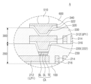
도 1을 참조하여, 본 발명의 실시예들에 따른 반도체 패키지(10)는 재배선 기판(400), 반도체 칩(500) 및 몰딩층(600)을 포함할 수 있다.Referring to FIG. 1 , a
재배선 기판(400)은 반도체 칩(500)의 하면과 몰딩층(600)의 하면 상에 제공될 수 있다. 재배선 기판(400)의 두께는 반도체 칩(500)의 두께보다 작을 수 있다. 재배선 기판(400)은 적어도 하나의 배선층을 포함할 수 있다. 배선층은 복수 개로 제공될 수 있다. 실시예에서, 재배선 기판(400)은 제 1 배선층(200) 및 제 2 배선층(300)을 포함할 수 있다. 이하, 도 1과 도 2를 함께 참조하여 재배선 기판(400)에 대해 상세히 설명한다.The
도 1을 참조하여, 지지 기판(100)이 제공될 수 있다. 지지 기판(100)은 실리콘 기판 또는 절연 기판을 포함할 수 있다. 지지 기판(100)은 필요에 따라 제공되지 않을 수 있다.Referring to FIG. 1, a
지지 기판(100) 상에 제 1 배선층(200)이 제공될 수 있다. 제 1 배선층(200)은 제 1 도전 패턴(210), 제 1 비아들(220), 제 1 절연층(230) 및 커패시터(CA)를 포함할 수 있다.A
지지 기판(100) 상에 제 1 도전 패턴(210)이 제공될 수 있다. 제 1 도전 패턴(210)은 하부 패드들(212) 및 제 1 배선들(214)을 포함할 수 있다. 여기서, 제 1 배선들(214)은 지지 기판(100)의 상면과 평행한 방향으로 연장되어 전기 회로를 구성하는 구성 요소로 정의되고, 하부 패드들(212)은 제 1 배선들(214)보다 넓은 폭을 갖도록 형성되어 제 1 배선들(214) 및 제 1 비아들(220)이 접속되는 구성 요소로 정의될 수 있다. 하부 패드들(212)은 서로 이격되어 배치되는 제 1 하부 패드(LP1) 및 제 2 하부 패드(LP2)를 포함할 수 있다. 제 1 배선들(214)은 하부 패드들(212)의 사이(예를 들어, 제 1 하부 패드(LP1)과 제 2 하부 패드(LP2)의 사이) 또는 하부 패드들(212)의 일측에 위치할 수 있다. 제 1 배선들(214)은 하부 패드들(212)과 전기적으로 연결될 수 있다. 이하에서, 전기적으로 연결된다는 것은 직접 또는 간접적으로 연결되는 것을 포함할 수 있다. 제 1 도전 패턴(210)은 도전성 물질을 포함할 수 있다. 예를 들면, 제 1 도전 패턴(210)은 구리(Cu), 구리 합금 또는 알루미늄(Al)을 포함할 수 있다.A first
제 1 도전 패턴(210)과 지지 기판(100) 사이에 제 1 시드막(216)이 제공될 수 있다. 제 1 시드막(216)은 구리(Cu)를 포함할 수 있다. 제 1 시드막(216)은 약 5Å 내지 50Å의 두께를 가질 수 있다.A
제 1 도전 패턴(210) 상에 제 1 비아들(220)이 배치될 수 있다. 일 예로, 제 1 비아들(220)은 하부 패드들(212)의 적어도 하나의 상면 상에 배치될 수 있다. 여기서, 제 1 비아들(220)은 제 1 배선층(200) 내의 제 1 도전 패턴(210)과 제 2 배선층(300)의 후술되는 제 2 도전 패턴(310)을 수직으로 연결하는 구성 요소로 정의될 수 있다. 제 1 비아들(220)의 측면은 제 1 도전 패턴(210)의 상면에 경사질 수 있다. 상세하게는, 제 1 비아들(220)은 제 1 도전 패턴(210)으로부터 멀어질수록 큰 폭을 갖는 테이퍼진(tapered) 형상을 가질 수 있다. 제 1 비아들(220)은 제 1 하부 패드(LP1) 상에 제공되는 제 1 서브 비아(222) 및 제 2 하부 패드(LP2) 상에 제공되는 제 2 서브 비아(224)를 포함할 수 있다. 제 1 비아들(220)은 하부 패드들(212)을 통해 제 1 배선들(214)에 전기적으로 연결될 수 있다. 제 1 비아들(220)은 도전성 물질을 포함할 수 있다. 예를 들면, 제 1 비아들(220)은 구리(Cu), 구리 합금 또는 알루미늄(Al)을 포함할 수 있다.
제 1 서브 비아(222)와 제 1 하부 패드(LP1) 사이에 커패시터(CA)가 제공될 수 있다. 커패시터(CA)는 제 1 하부 패드(LP1)의 상면 상에 배치될 수 있다. 제 1 하부 패드(LP1), 커패시터(CA) 및 제 1 서브 비아(222)는 수직으로 중첩될 수 있다. 커패시터(CA)의 폭은 제 1 하부 패드(LP1)의 폭과 같거나 작을 수 있다. 커패시터(CA)의 폭은 제 1 서브 비아(222)의 폭과 같거나 클 수 있다. 커패시터(CA)는 순차적으로 적층되는 베리어층(BL), 유전층(DL) 및 상부 전극(TE)을 포함할 수 있다. 이때, 베리어층(BL)의 폭, 유전층(DL)의 폭 및 상부 전극(TE)의 폭을 동일할 수 있다. 제 1 하부 패드(LP1)는 커패시터(CA)의 하부 전극의 역할을 할 수 있다. 이하, 도 2를 함께 참조하여 커패시터(CA)의 구성을 상세히 설명한다.A capacitor CA may be provided between the
도 1 및 도 2를 참조하여, 제 1 하부 패드(LP1) 상에 베리어층(BL)이 배치될 수 있다. 베리어층(BL)은 타이타늄 질화물(TiN), 타이타늄 알루미늄(TiAl), 타이타늄 알루미늄 질화물(TiAlN), 타이타늄 질화물(TiN)을 함유하는 금속 화합물, 탄탈럼 질화물(TaN), 탄탈럼 알루미늄 질화물(TaAlN), 탄탈럼 알루미늄 탄질화물(TaAlCN) 또는 탄탈럼 질화물(TaN)을 함유하는 금속 화합물을 포함할 수 있다. 베리어층(BL)은 제 1 하부 패드(LP1)와 함께 커패시터(CA)의 하부 전극의 역할을 할 수 있다. 베리어층(BL)은 제 1 하부 패드(LP1)의 금속 물질이 유전층(DL)으로 확산되는 것을 방지할 수 있다Referring to FIGS. 1 and 2 , a barrier layer BL may be disposed on the first lower pad LP1. The barrier layer (BL) is made of titanium nitride (TiN), titanium aluminum (TiAl), titanium aluminum nitride (TiAlN), a metal compound containing titanium nitride (TiN), tantalum nitride (TaN), and tantalum aluminum nitride (TaAlN). , it may include a metal compound containing tantalum aluminum carbonitride (TaAlCN) or tantalum nitride (TaN). The barrier layer BL may serve as a lower electrode of the capacitor CA together with the first lower pad LP1. The barrier layer BL may prevent the metal material of the first lower pad LP1 from diffusing into the dielectric layer DL.
베리어층(BL) 상에 유전층(DL)이 배치될 수 있다. 유전층(DL)은 고유전(high-K) 물질을 포함할 수 있다. 예를 들어, 고유전 물질은 실리콘 질화물(SiNx), 지르코늄 산화물(ZrO2), 하프늄 산화물(HfO2), 타이타늄 산화물(TiO2), 탄탈럼 산화물(Ta2O5), 알루미늄 산화물(Al2O3), 스트론튬 타이타늄 산화물(SrTiO3) 또는 바륨 타이타늄 산화물(BaTiO3)을 포함하나, 이에 한정되지 않는다.A dielectric layer (DL) may be disposed on the barrier layer (BL). The dielectric layer DL may include a high-k material. For example , high dielectric materials include silicon nitride ( SiN 2 O 3 ), strontium titanium oxide (SrTiO 3 ), or barium titanium oxide (BaTiO 3 ), but is not limited thereto.
유전층(DL) 상에 상부 전극(TE)이 배치될 수 있다. 상부 전극(TE)은 도전 물질을 포함할 수 있다. 상부 전극(TE)은 금속 또는 도전성의 금속 화합물을 포함할 수 있다. 일 예로, 금속 화합물은 타이타늄 질화물(TiN), 타이타늄 알루미늄(TiAl), 타이타늄 알루미늄 질화물(TiAlN), 타이타늄 질화물(TiN)을 함유하는 금속 화합물, 탄탈럼 질화물(TaN), 탄탈럼 알루미늄 질화물(TaAlN), 탄탈럼 알루미늄 탄질화물(TaAlCN) 또는 탄탈럼 질화물(TaN)을 함유하는 금속 화합물을 포함할 수 있다. 상부 전극(TE)은 커패시터(CA)의 전극 역할을 할 수 있다. 상부 전극(TE)이 금속 화합물을 포함하는 경우, 상부 전극(TE)은 후술되는 제 2 도전 패턴(310)의 금속 물질이 유전층(DL)으로 확산되는 것을 방지할 수 있다An upper electrode (TE) may be disposed on the dielectric layer (DL). The upper electrode (TE) may include a conductive material. The upper electrode (TE) may include metal or a conductive metal compound. For example, the metal compound is titanium nitride (TiN), titanium aluminum (TiAl), titanium aluminum nitride (TiAlN), a metal compound containing titanium nitride (TiN), tantalum nitride (TaN), tantalum aluminum nitride (TaAlN). , it may include a metal compound containing tantalum aluminum carbonitride (TaAlCN) or tantalum nitride (TaN). The upper electrode (TE) may serve as an electrode of the capacitor (CA). When the upper electrode TE includes a metal compound, the upper electrode TE can prevent the metal material of the second
커패시터(CA)가 제 1 하부 패드(LP1) 상에 제공됨에 따라, 제 1 서브 비아(222)는 제 1 하부 패드(LP1) 상에서 커패시터(CA) 및 제 2 배선층(300)의 후술되는 제 2 도전 패턴(310)을 연결하고, 제 2 서브 비아(224)는 제 2 하부 패드(LP2) 상에서 제 2 하부 패드(LP2) 및 제 2 배선층(300)의 제 2 도전 패턴(310)을 연결할 수 있다. 제 1 서브 비아(222)는 커패시터(CA)의 상면 상에 접속되고, 제 2 서브 비아(224)는 제 2 하부 패드(LP2)의 상면 상에 접속될 수 있다. 이에 따라, 제 1 서브 비아(222)의 높이는 제 2 서브 비아(224)의 높이보다 낮을 수 있다. 상세하게는, 제 1 서브 비아(222)의 높이와 커패시터(CA)의 높이의 합은 제 2 서브 비아(224)의 높이와 동일할 수 있다.As the capacitor CA is provided on the first lower pad LP1, the
도 1을 계속 참조하여, 지지 기판(100) 상에 제 1 절연층(230)이 제공될 수 있다. 제 1 절연층(230)은 제 1 도전 패턴(210)을 덮고, 제 1 비아들(220)을 둘러쌀 수 있다. 제 1 절연층(230)은 제 1 하부 패드(LP1)의 상면의 적어도 일부, 제 2 하부 패드(LP2)의 상면, 및 커패시터(CA)의 측면(즉, 베리어층(BL)의 측면, 유전층(DL)의 측면 및 상부 전극(TE)의 측면)과 접할 수 있다. 이때, 커패시터(CA)의 폭이 제 1 하부 패드(LP1)의 폭과 동일한 경우, 제 1 절연층(230)은 제 1 하부 패드(LP1)의 상면과 접하지 않을 수도 있다. 제 1 절연층(230)의 상면은 제 1 비아들(220)의 상면과 공면(coplanar)을 이룰 수 있다. 제 1 절연층(230)은 실리콘 산화물(SiOx), 실리콘 질화물(SiNx), 실리콘 산화질화물(SiON)과 같은 무기 물질 및/또는 폴리아미드 계열의 고분자 물질을 포함하나, 이에 한정되지 않는다.Continuing to refer to FIG. 1 , a first insulating
제 1 비아들(220)과 제 1 도전 패턴(210) 사이에 제 2 시드막(316)이 제공될 수 있다. 제 2 시드막(316)은 제 1 비아들(220)의 하면 및 측면을 덮을 수 있다. 제 2 시드막(316)은 제 1 하부 패드(LP1) 상에서 커패시터(CA)와 제 1 서브 비아(222) 사이에 개재될 수 있고, 제 2 하부 패드(LP2) 상에서 제 2 하부 패드(LP2)와 제 2 서브 비아(224) 사이에 개재될 수 있다. 제 2 시드막(316)은 제 1 비아들(220)과 제 1 절연층(230)을 이격시킬 수 있다. 제 2 시드막(316)은 제 2 도전 패턴(310)과 제 1 절연층(230) 사이로 연장될 수 있다. 즉, 제 2 시드막(316)은 제 2 도전 패턴(310)의 하면 상에 제공될 수 있다. 제 2 시드막(316)은 구리(Cu)를 포함할 수 있다. 제 2 시드막(316)은 약 5Å 내지 50 Å의 두께를 가질 수 있다.A
제 2 배선층(300)은 제 1 배선층(200) 상에 제공될 수 있다. 제 2 배선층(300)은 제 2 도전 패턴(310), 제 2 비아(320) 및 제 2 절연층(330)을 포함할 수 있다.The
제 1 배선층(200) 상에 제 2 도전 패턴(310)이 제공될 수 있다. 제 2 도전 패턴(310)은 상부 패드들(312) 및 제 2 배선들(314)을 포함할 수 있다. 여기서, 제 2 배선들(314)은 제 1 배선층(200)의 상면과 평행한 방향으로 연장되어 전기 회로를 구성하는 구성 요소로 정의되고, 상부 패드들(312)은 제 2 배선들(314)보다 넓은 폭으로 형성되어 제 2 배선들(314) 및 제 2 비아들(320)이 접속되는 구성 요소로 정의될 수 있다. 상부 패드들(312)은 서로 이격되어 배치되는 제 1 상부 패드(UP1) 및 제 2 상부 패드(UP2)를 포함할 수 있다. 상부 패드들(312) 중 일부는 제 1 비아들(220) 상에 배치되어, 제 1 비아들(220)에 접속될 수 있다. 예를 들어, 제 1 상부 패드(UP1)는 제 1 서브 비아(222)와 접하고, 제 2 상부 패드(UP2)는 제 2 서브 비아(224)와 접할 수 있다. 이때, 제 1 상부 패드(UP1)와 제 1 하부 패드(LP1) 사이의 간격은 제 2 상부 패드(UP2)와 제 2 하부 패드(LP2) 사이의 간격과 동일할 수 있다. 상부 패드들(312)은 제 1 비아들(220)을 통해 하부 패드들(212)과 전기적으로 연결될 수 있다. 예를 들어, 제 1 상부 패드(UP1)는 제 1 서브 비아(222) 및 커패시터(CA)를 통해 제 1 하부 패드(LP1)와 연결되고, 제 2 상부 패드(UP2)는 제 2 서브 비아(224)를 통해 제 2 하부 패드(LP2)와 연결될 수 있다. 제 2 배선들(314)은 제 1 절연층(230) 상에 배치될 수 있다. 평면적 관점에서, 제 2 배선들(314)은 상부 패드들(312)의 사이 또는 상부 패드들(312)의 일측에 위치할 수 있다. 제 2 배선들(314)은 재배선 역할을 할 수 있다. 제 2 배선들(314)은 상부 패드들(312)과 전기적으로 연결될 수 있다. 제 2 도전 패턴(310)의 일부는 제 1 비아들(220)과 일체로 제공될 수 있다. 예를 들어, 제 2 도전 패턴(310)의 일부는 제 1 비아들(220)과 동일한 물질을 포함할 수 있다. 제 2 도전 패턴(310)은 도전성 물질을 포함할 수 있다. 예를 들면, 제 2 도전 패턴(310)은 구리(Cu), 구리 합금 또는 알루미늄(Al)을 포함할 수 있다.A second
제 2 도전 패턴(310) 상에 제 2 비아들(320)이 배치될 수 있다. 제 2 비아들(320)은 상부 패드들(312)의 상면 상에 각각 배치될 수 있다. 여기서, 제 2 비아들(320)은 제 2 배선층(300) 내의 제 2 도전 패턴(310)과 후술되는 언더 범프 패드들(340)을 수직으로 연결하는 구성 요소로 정의될 수 있다. 제 2 비아들(320)의 측면은 제 2 도전 패턴(310)의 상면에 경사질 수 있다. 상세하게는, 제 2 비아들(320)은 제 2 도전 패턴(310)으로부터 멀어질수록 큰 폭을 갖는 테이퍼진(tapered) 형상을 가질 수 있다. 제 2 비아들(320)은 상부 패드들(312)을 통해 제 2 배선들(314)에 전기적으로 연결될 수 있다. 제 2 비아들(320)은 도전성 물질을 포함할 수 있다.
제 1 배선층(200) 상에 제 2 절연층(330)이 제공될 수 있다. 제 2 절연층(330)은 제 2 도전 패턴(310)을 덮고, 제 2 비아들(320)을 둘러쌀 수 있다. 제 2 절연층(330)은 제 2 도전 패턴(310)의 측면과 접할 수 있다. 제 2 절연층(330)은 실리콘 산화물(SiOx), 실리콘 질화물(SiNx), 실리콘 산화질화물(SiON)과 같은 무기 물질 및/또는 폴리아미드 계열의 고분자 물질을 포함하나, 이에 한정되지 않는다.A second insulating
제 2 비아들(320)의 상면 상에 언더 범프 패드들(340)이 배치될 수 있다. 언더 범프 패드들(340)는 제 2 비아들(320)보다 넓은 폭으로 형성되어 제 2 비아들(320) 및 반도체 칩(500)의 후술되는 연결 단자들(510)이 접속되는 구성 요소로 정의될 수 있다. 언더 범프 패드들(340)의 폭은 상부 패드들(312)의 폭보다 클 수 있다. 언더 범프 패드들(340)의 폭은 제 2 비아들(320)의 상면의 폭보다 클 수 있다. 언더 범프 패드들(340)은 제 2 비아들(320)과 일체로 제공될 수 있다. 예를 들어, 언더 범프 패드들(340)은 제 2 비아들(320)과 동일한 물질을 포함할 수 있다. 언더 범프 패드들(340)은 도전성 물질을 포함할 수 있다.Under
제 1 도전 패턴(210)은 제 1 절연층(230) 내에서 제 1 절연층(230)의 상면과 평행한 방향으로 연장되는 회로들(예를 들어, 제 1 배선들(214) 및 하부 패드들(212))을 포함하고, 제 2 도전 패턴(310)은 제 2 절연층(330) 내에서 제 2 절연층(330)의 상면과 평행한 방향으로 연장되는 회로들(예를 들어, 제 2 배선들(314) 및 상부 패드들(312))을 포함할 수 있다. 제 1 비아들(220)은 제 1 도전 패턴(210)과 제 2 도전 패턴(310)을 상하로 연결하고, 제 2 도전 패턴(310)과 언더 범프 패드들(340)을 상하로 연결할 수 있다.The first
본 발명의 실시예들에 따르면, 커패시터(CA)는 재배선 기판(400) 내에 제공될 수 있다. 상세하게는, 커패시터(CA)가 제 1 배선층(200)의 제 1 도전 패턴(210)과 제 2 배선층(300)의 제 2 도전 패턴(310) 사이에 제공되며, 재배선 기판(400)의 도전 패턴들(210, 310)이 커패시터(CA)의 전극들로 이용될 수 있다. 즉, 재배선 기판(400)은 그의 내부에 커패시터(CA)를 배치하기 위한 별도의 공간이 필요하지 않을 수 있으며, 재배선 기판(400) 및 이를 포함하는 반도체 패키지(10)의 소형화에 기여할 수 있다. 더하여, 커패시터(CA)는 베리어층(BL)을 포함하여 커패시터(CA)의 전극으로 이용되는 제 1 도전 패턴(210)으로부터 금속 물질이 확산되어 유전층(DL)이 손상되는 것을 방지할 수 있다. 즉, 재배선 기판(400) 및 이를 포함하는 반도체 패키지(10)의 신뢰성이 향상될 수 있다.According to embodiments of the present invention, the capacitor CA may be provided in the
도 1을 계속 참조하여, 제 2 비아들(320)과 제 2 도전 패턴(310) 사이에 제 3 시드막(322)이 제공될 수 있다. 제 3 시드막(322)은 제 2 비아들(320)의 하면으로부터 제 2 비아들(320)의 측면을 따라 제 2 절연층(330)과 언더 범프 패드들(340) 사이로 연장될 수 있다. 즉, 제 3 시드막(322)은 제 2 비아들(320) 및 언더 범프 패드들(340)과 제 2 절연층(330)을 이격시킬 수 있다. 이상과 같이, 본 발명에 따른 재배선 기판(400)이 제공될 수 있다.Continuing to refer to FIG. 1 , a
반도체 칩(500)은 재배선 기판(400)의 상면 상에 위치될 수 있다. 재배선 기판(400)을 향하는 반도체 칩(500)의 하면은 활성면일 수 있다. 반도체 칩(500)은 실리콘(Si)을 포함할 수 있다. 반도체 칩(500)은 재배선 기판(400)에 플립 칩(flip chip) 방식으로 실장될 수 있다. 일 예로, 반도체 칩(500)은 그의 하면 상에 제공된 연결 단자들(510)을 가질 수 있다. 연결 단자들(510)은 재배선 기판(400)의 언더 범프 패드들(340)에 접속될 수 있다. 연결 단자들(510)은 솔더 볼 또는 솔더 범프를 포함할 수 있다. 반도체 칩(500)은 재배선 기판(400)의 언더 범프 패드들(340) 및 제 2 비아들(320)을 통해 제 2 배선들(314)과 전기적으로 연결될 수 있다. 재배선 기판(400)은 제 2 배선들(314)을 이용하여 반도체 칩(500)을 재배선할 수 있다.The
다른 실시예들에 따르면, 재배선 기판(400) 상에 제공되는 반도체 칩(500)은 그의 내부에 트랜지스터를 포함하지 않을 수 있다. 즉, 도시된 바와는 다르게, 재배선 기판(400) 상에 칩(chip)이 아닌 인터포저(interposer) 기판이 배치될 수 있다. 상기 인터포저 기판은 실리콘(Si)을 포함할 수 있다. 상기 인터포저 기판은 그의 상면 상에 배선을 위한 회로를 가질 수 있다. 상기 인터포저 기판은 필요에 따라 몰드막에 의해 둘러싸일 수 있다. 여기서, 상기 몰드막은 후술되는 몰딩층(600)과 구별되는 구성요소이다. 상기 몰드막은 재배선 기판(400) 상에서 상기 인터포저 기판을 매립할 수 있다. 즉, 상기 인터포저 기판은 상기 몰드막에 의해 덮일 수 있다. 상기 인터포저 기판 상에는 적어도 하나의 소자(일 예로, 트랜지스터를 포함하는 칩 또는 반도체 패키지 내에서 요구되는 전자 소자 등)가 제공될 수 있다. 상기 적어도 하나의 소자는 상기 몰드막 또는 상기 인터포저 기판을 관통하는 비아(via) 등을 이용하여 재배선 기판(400) 및 상기 인터포저 기판에 전기적으로 연결될 수 있다. 또는, 상기 몰드막이 제공되지 않는 경우, 상기 적어도 하나의 소자는 상기 인터포저 기판 상이 직접 실장될 수 있다. 상기 소자가 복수로 제공되는 경우, 상기 소자들은 상기 인터포저 기판을 통해 상호 전기적으로 연결될 수 있다. 필요에 따라, 상기 적어도 하나의 소자와 상기 인터포저 기판(또는 상기 몰드막) 사이에 상기 적어도 하나의 소자를 지지하기 위한 추가 기판이 제공될 수 있다. 이때, 상기 적어도 하나의 소자는 상기 추가 기판에 실장될 수 있으며, 상기 적어도 하나의 소자는 상기 추가 기판 및 상기 비아를 통해 상기 인터포저 기판과 재배선 기판(400)에 전기적으로 연결될 수 있다. 이하, 재배선 기판(400) 상에 반도체 칩(500)이 제공되는 것을 기준으로 계속 설명한다.According to other embodiments, the
몰딩층(600)은 재배선 기판(400) 상에 제공될 수 있다. 몰딩층(600)은 재배선 기판(400)의 상면 상에서 반도체 칩(500)을 덮을 수 있다. 예를 들어, 몰딩층(600)은 반도체 칩(500)의 상면 및 측면을 덮을 수 있다. 몰딩층(600)은 반도체 칩(500)과 재배선 기판(400) 사이의 공간을 채울 수 있다. 몰딩층(600)은 에폭시계 폴리머와 같은 절연 물질을 포함할 수 있다. 이와는 다르게, 반도체 칩(500)과 재배선 기판(400) 사이의 공간은 언더필(under fill) 부재로 채워질 수 있다.The
도 3은 본 발명의 실시예들에 따른 반도체 패키지를 설명하기 위한 단면도이다. 도 4는 도 3의 B영역을 확대 도시한 도면이다. 이하 앞서 설명한 바와 중복되는 내용은 설명의 편의를 위하여 생략한다.Figure 3 is a cross-sectional view for explaining a semiconductor package according to embodiments of the present invention. FIG. 4 is an enlarged view of area B of FIG. 3. Hereinafter, content that overlaps with what was previously described will be omitted for convenience of explanation.
도 3 및 도 4를 참조하여, 커패시터(CA)는 제 1 비아들(220)과 동일/유사한 형상을 가질 수 있다. 상세하게는, 제 1 서브 비아(222)는 제 2 도전 패턴(310)으로부터 멀어질수록 작아지는 폭을 갖는 테이퍼진(tapered) 형상을 갖고, 커패시터(CA)는 제 1 서브 비아(222)로부터 멀어질수록 작아지는 폭을 갖는 테이퍼진 형상을 가질 수 있다. 이때, 커패시터(CA)의 측면은 제 1 서브 비아(222)의 측면과 공면(coplanar)을 이룰 수 있다. 이에 따라, 상부 전극(TE)의 폭이 유전층(DL)의 폭보다 크고, 유전층(DL)의 폭이 베리어층(BL)의 폭보다 클 수 있다. 커패시터(CA)의 상면의 폭은 제 1 서브 비아(222)의 하면의 폭과 동일할 수 있다.Referring to FIGS. 3 and 4 , the capacitor CA may have the same/similar shape as the
다른 실시예들에 따르면, 재배선 기판(400)은 둘 이상의 배선층들을 포함할 수 있다. 도 5는 본 발명의 실시예들에 따른 반도체 패키지를 설명하기 위한 단면도이다.According to other embodiments, the
도 5를 참조하여, 재배선 기판(400)은 제 1 배선층(200)과 제 2 배선층(300) 사이에 제공되는 제 3 배선층(700)을 더 포함할 수 있다. 지지 기판(100) 상에 제 1 배선층(200), 제 2 배선층(300) 및 제 3 배선층(700)이 제공될 수 있다.Referring to FIG. 5 , the
제 1 배선층(200)은 제 1 도전 패턴(210), 제 1 비아들(220), 제 1 절연층(230) 및 제 1 커패시터(CA1)를 포함할 수 있다. 제 1 커패시터(CA1)는 제 1 도전 패턴(210)의 제 1 하부 패드(LP1)의 상면 상에 순차적으로 적층되는 제 1 베리어층(BL1), 제 1 유전층(DL1) 및 제 1 상부 전극(TE1)을 포함할 수 있다. 제 1 비아들(220)은 제 1 커패시터(CA1) 및 제 2 하부 패드(LP2)에 접속될 수 있다.The
제 2 배선층(300)은 제 1 배선층(200) 상에 제공될 수 있다. 제 2 배선층(300)은 제 2 도전 패턴(310), 제 2 비아(320) 및 제 2 절연층(330)를 포함할 수 있다.The
제 3 배선층(700)은 제 1 배선층(200)과 제 2 배선층(300) 사이에 제공될 수 있다. 제 3 배선층(700)은 제 3 도전 패턴(710), 제 3 비아들(720) 및 제 3 절연층(730)을 포함할 수 있다.The
제 1 배선층(200) 상에 제 3 도전 패턴(710)이 제공될 수 있다. 제 3 도전 패턴(710)은 중간 패드들(712) 및 제 3 배선들(714)을 포함할 수 있다. 중간 패드들(712)의 일부는 제 1 비아들(220) 상에 배치되어, 제 1 비아들(220)에 접속될 수 있다. 중간 패드들(712)의 폭은 제 1 비아들(220)의 폭보다 클 수 있다. 중간 패드들(712)은 서로 이격되어 배치되는 제 1 중간 패드(MP1) 및 제 2 중간 패드(MP2)를 포함할 수 있다. 제 3 배선들(714)은 중간 패드들(712)의 사이 또는 중간 패드들(712)의 일측에 위치할 수 있다. 제 3 배선들(714)은 재배선 역할을 할 수 있다.A third
제 3 도전 패턴(710) 상에 제 3 비아들(720)이 배치될 수 있다. 일 예로, 제 3 비아들(720)은 중간 패드들(712)의 적어도 하나의 상면 상에 배치될 수 있다. 중간 패드들(712) 상의 제 3 비아들(720)은 상부 패드들(312)에 접속될 수 있다. 제 3 비아들(720)은 제 3 도전 패턴(710)으로부터 멀어질수록 큰 폭을 갖는 테이퍼진(tapered) 형상을 가질 수 있다. 제 3 비아들(720)은 제 1 중간 패드(MP1) 상에 제공되는 제 3 서브 비아(722) 및 제 2 중간 패드(MP2) 상에 제공되는 제 4 서브 비아(724)를 포함할 수 있다. 제 3 비아들(720)은 중간 패드들(712)을 통해 제 3 배선들(714)에 전기적으로 연결될 수 있다.
제 3 서브 비아(722)와 제 1 중간 패드(MP1) 사이에 제 2 커패시터(CA2)가 제공될 수 있다. 제 2 커패시터(CA2)는 제 1 중간 패드(MP1)의 상면 상에 배치될 수 있다. 제 2 커패시터(CA2)의 폭은 제 1 중간 패드(MP1)의 폭과 같거나 작을 수 있다. 제 2 커패시터(CA2)의 폭은 제 3 서브 비아(722)의 폭과 같거나 클 수 있다. 제 2 커패시터(CA2)는 순차적으로 적층되는 제 2 베리어층(BL2), 제 2 유전층(DL2) 및 제 2 상부 전극(TE2)을 포함할 수 있다. 이때, 제 2 베리어층(BL2)의 폭, 제 2 유전층(DL2)의 폭 및 제 2 상부 전극(TE2)의 폭을 동일할 수 있다. 제 1 중간 패드(MP1)는 제 2 커패시터(CA2)의 하부 전극의 역할을 할 수 있다.A second capacitor CA2 may be provided between the
제 1 중간 패드(MP1) 상에 제 2 베리어층(BL2)이 배치될 수 있다. 제 2 베리어층(BL2)은 제 1 중간 패드(MP1)와 함께 제 2 커패시터(CA2)의 하부 전극의 역할을 할 수 있다. 제 2 베리어층(BL2)은 제 1 중간 패드(MP1)의 금속 물질이 제 2 유전층(DL2)으로 확산되는 것을 방지할 수 있다The second barrier layer BL2 may be disposed on the first intermediate pad MP1. The second barrier layer BL2 may serve as a lower electrode of the second capacitor CA2 together with the first intermediate pad MP1. The second barrier layer BL2 may prevent the metal material of the first intermediate pad MP1 from diffusing into the second dielectric layer DL2.
제 2 베리어층(BL2) 상에 제 2 유전층(DL2)이 배치될 수 있다. 제 2 유전층(DL2)은 고유전(high-K) 물질을 포함할 수 있다.The second dielectric layer DL2 may be disposed on the second barrier layer BL2. The second dielectric layer DL2 may include a high-k material.
제 2 유전층(DL2) 상에 제 2 상부 전극(TE2)이 배치될 수 있다. 제 2 상부 전극(TE2)은 도전 물질을 포함할 수 있다. 제 2 상부 전극(TE2)은 제 2 커패시터(CA2)의 전극 역할을 할 수 있다. 제 2 상부 전극(TE2)이 금속 화합물을 포함하는 경우, 제 2 상부 전극(TE2)은 제 2 도전 패턴(310)의 금속 물질이 제 2 유전층(DL2)으로 확산되는 것을 방지할 수 있다The second upper electrode TE2 may be disposed on the second dielectric layer DL2. The second upper electrode TE2 may include a conductive material. The second upper electrode TE2 may serve as an electrode of the second capacitor CA2. When the second upper electrode TE2 includes a metal compound, the second upper electrode TE2 may prevent the metal material of the second
제 2 커패시터(CA2)가 제 1 중간 패드(MP1) 상에 제공됨에 따라, 제 3 서브 비아(722)는 제 1 중간 패드(MP1) 상에서 제 2 커패시터(CA2) 및 제 2 배선층(300)의 제 2 도전 패턴(310)을 연결하고, 제 4 서브 비아(724)는 제 2 중간 패드(MP2) 상에서 제 2 중간 패드(MP2) 및 제 2 배선층(300)의 제 2 도전 패턴(310)을 연결할 수 있다. 제 3 서브 비아(722)는 제 2 커패시터(CA2)의 상면 상에 접속되고, 제 4 서브 비아(724)는 제 2 중간 패드(MP2)의 상면 상에 접속될 수 있다. 이에 따라, 제 3 서브 비아(722)의 높이는 제 4 서브 비아(724)의 높이보다 낮을 수 있다. 상세하게는, 제 3 서브 비아(722)의 높이와 제 2 커패시터(CA2)의 높이의 합은 제 4 서브 비아(724)의 높이와 동일할 수 있다.As the second capacitor CA2 is provided on the first intermediate pad MP1, the
제 3 비아들(720)과 제 3 도전 패턴(710) 사이에 제 4 시드막(716)이 제공될 수 있다. 제 4 시드막(716)은 제 3 비아들(720)의 하면으로부터 제 3 비아들(720)의 측면을 따라 제 3 절연층(730)과 제 2 도전 패턴(310) 사이로 연장될 수 있다.A
제 1 배선층(200) 상에 제 3 절연층(730)이 제공될 수 있다. 제 3 절연층(730)은 제 3 도전 패턴(710) 및 제 2 커패시터(CA2)를 덮고, 제 3 비아들(720)을 둘러쌀 수 있다. 제 3 절연층(730)은 제 3 비아들(720)의 측면, 제 2 커패시터(CA2)의 상면 및 제 3 도전 패턴(710)의 상면과 접할 수 있다. 제 3 절연층(730)은 제 2 배선층(300)의 하면과 접할 수 있다.A third insulating
도 5에서 3개의 배선층들(200, 300, 700)을 포함하는 재배선 기판(400)을 개시하였으나, 본 발명이 이에 한정되는 것은 아니다. 재배선 기판(400)은 셋 이상의 복수의 배선층들을 포함할 수 있다.Although the
본 발명의 실시예들에 따르면, 복수의 커패시터들(CA1, CA2)은 재배선 기판(400) 내에 제공될 수 있다. 즉, 재배선 기판(400)은 그의 내부에 커패시터들(CA1, CA2)을 배치하기 위한 별도의 공간이 필요하지 않을 수 있으며, 재배선 기판(400) 및 이를 포함하는 반도체 패키지(12)의 소형화에 기여할 수 있다.According to embodiments of the present invention, a plurality of capacitors CA1 and CA2 may be provided in the
다른 실시예들에 따르면, 재배선 기판(400)은 제 1 배선층(200) 아래에 외부 접속을 위한 외부 단자들이 제공될 수 있다. 도 6은 본 발명의 실시예들에 따른 반도체 패키지를 설명하기 위한 단면도이다.According to other embodiments, the
도 6을 참조하여, 재배선 기판(400)의 하면 상에 지지 기판(100, 도 1 참조)이 아닌 보호층(800)이 제공될 수 있다. 보호층(800)은 에폭시(epoxy)계 폴리머와 같은 절연성 폴리머, ABF(Ajinomoto Build-up Film), 유기물질 또는 무기물질을 포함할 수 있다. 외부 단자들(830)이 보호층(800)의 하면 상에 배치될 수 있다. 외부 단자들(830)은 보호층(800)을 관통하여 제 1 도전 패턴(210)과 접속되는 외부 패드들(810) 상에 배치될 수 있다. 외부 단자들(830)은 외부 패드들(810)을 통해 재배선 기판(400)의 하부 패드들(212)과 전기적으로 연결될 수 있다. 외부 패드들(810)과 보호층(800) 사이에 베리어 금속막(820)이 제공될 수 있다. 일 예로, 보호층(800)은 하부 패드들(212)을 노출시키는 리세스를 갖고, 베리어 금속막(820)은 상기 리세스의 바닥면 및 내벽을 덮을 수 있다. 외부 패드들(810)은 상기 리세스를 채우도록 베리어 금속막(820) 상에 배치될 수 있다. 외부 단자들(830)은 솔더 볼 또는 솔더 범프를 포함할 수 있다. 외부 패드들(810)은 구리(Cu)와 같은 금속을 포함할 수 있다. 베리어 금속막(820)은 탄탈럼(Ta), 탄탈럼 질화물(TaN), 탄탈럼 실리콘 질화물(TaSiN), 타이타늄(Ti), 타이타늄 질화물(TiN), 타이타늄 실리콘 질화물(TiSiN), 텅스텐(W), 및 텅스텐 질화물(WN) 중 적어도 하나를 포함할 수 있다.Referring to FIG. 6 , a
도 7 내지 도 19는 본 발명의 실시예들에 따른 재배선 기판의 제조 방법을 설명하기 위한 단면도들이다.7 to 19 are cross-sectional views for explaining a method of manufacturing a redistribution substrate according to embodiments of the present invention.
도 7을 참조하여, 지지 기판(100) 상에 제 1 도전 패턴(210)이 형성될 수 있다. 예를 들어, 지지 기판(100) 상에 제 1 시드막(216)을 형성한 후, 제 1 시드막(216) 상에 리세스들을 갖는 식각 마스크가 형성될 수 있다. 상기 리세스들은 제 1 도전 패턴(210)이 형성되는 영역을 정의할 수 있다. 도금 공정 등을 통해 상기 리세스들 내에 도전 물질을 채워 제 1 도전 패턴(210)이 형성될 수 있다. 이후, 상기 식각 마스크와 제 1 시드막(216)의 일부가 제거될 수 있다. 제 1 시드막(216)은 지지 기판(100)과 제 1 도전 패턴(210) 사이에 잔여할 수 있다. 또는, 지지 기판(100) 상에 도전 물질을 증착한 후, 상기 도전 물질을 패터닝하여 제 1 도전 패턴(210)이 형성될 수 있다. 제 1 도전 패턴(210)은 하부 패드들(212) 및 제 1 배선들(214)을 포함할 수 있다. 하부 패드들(212) 제 1 하부 패드(LP1) 및 제 2 하부 패드(LP2)를 포함할 수 있다.Referring to FIG. 7 , a first
도 8을 참조하여, 지지 기판(100) 상에 제 1 마스크 패턴(MSP1)이 형성될 수 있다. 예를 들어, 지지 기판(100), 제 1 도전 패턴(210) 및 제 1 시드막(216) 상에 감광성 하드마스크 물질을 도포하여 제 1 마스크 패턴(MSP1)이 형성될 수 있다. 감광성 하드마스크 물질은 레진, 감광 물질, 가교제, 및 용제를 포함할 수 있다.Referring to FIG. 8 , a first mask pattern MSP1 may be formed on the
이후, 제 1 마스크 패턴(MSP1)에 리세스(RS)가 형성될 수 있다. 예를 들어, 제 1 마스크 패턴(MSP1) 중 노광된 부분은 현상액에 의해 용해되고, 노광되지 않은 부분은 현상액에 의해 용해되지 않을 수 있다. 리세스(RS)는 제 1 마스크 패턴(MSP1)을 관통하여 제 1 하부 패드(LP1)의 상면을 노출할 수 있다. 리세스(RS)의 폭은 제 1 하부 패드(LP1)의 폭과 같거나 작을 수 있다.Afterwards, a recess RS may be formed in the first mask pattern MSP1. For example, the exposed portion of the first mask pattern MSP1 may be dissolved by the developer, and the unexposed portion may not be dissolved by the developer. The recess RS may penetrate the first mask pattern MSP1 and expose the top surface of the first lower pad LP1. The width of the recess RS may be equal to or smaller than the width of the first lower pad LP1.
이와는 다르게, 도 9에 도시된 바와 같이, 제 1 마스크 패턴(MSP1)은 사전에 리세스(RS)가 형성된 마스크일 수 있다. 이 경우, 제 1 마스크 패턴(MSP1)은 평판 형태를 가질 수 있으며, 제 1 도전 패턴(210) 상에 배치될 수 있다. 제 1 마스크 패턴(MSP1)은 제 1 도전 패턴(210)을 사이에 두고 지지 기판(100)과 이격될 수 있으며, 제 1 도전 패턴(210)의 하부 패드들(212) 사이의 공간, 하부 패드들(212)과 제 1 배선들(214) 사이의 공간, 및 제 1 배선들(214) 사이의 공간에 공극(AG)이 형성될 수 있다. 사전에 리세스(RS)가 형성된 제 1 마스크 패턴(MSP1)은 금속 마스크 또는 절연 물질을 포함하는 하드 마스크일 수 있다. 이하, 도 8을 기준으로 계속 설명한다.Alternatively, as shown in FIG. 9 , the first mask pattern MSP1 may be a mask in which a recess RS is formed in advance. In this case, the first mask pattern MSP1 may have a flat shape and may be disposed on the first
도 10을 참조하여, 제 1 마스크 패턴(MSP1)의 리세스(RS) 내에 커패시터(CA)가 형성될 수 있다. 예를 들어, 리세스(RS)에 의해 노출되는 제 1 하부 패드(LP1)의 상면 상에 베리어층(BL), 유전층(DL) 및 상부 전극(TE)이 순차적으로 증착될 수 있다. 베리어층(BL), 유전층(DL) 및 상부 전극(TE)은 화학 기상 증착(CVD) 공정 등을 이용하여 형성될 수 있다. 상세하게는, 제 1 하부 패드(LP1) 및 제 1 마스크 패턴(MSP1) 상에 베리어막을 증착한 후, 상기 베리어막이 리세스(RS) 내에 잔여하도록 패터닝 공정이 수행되어 베리어층(BL)이 형성될 수 있다. 베리어층(BL) 및 제 1 마스크 패턴(MSP1) 상에 유전막을 증착한 후, 상기 유전막이 리세스(RS) 내에 잔여하도록 패터닝 공정이 수행되어 유전층(DL)이 형성될 수 있다. 유전층(DL) 및 제 1 마스크 패턴(MSP1) 상에 도전막을 증착한 후, 상기 도전막이 리세스(RS) 내에 잔여하도록 패터닝 공정이 수행되어 상부 전극(TE)이 형성될 수 있다. 이후, 제 1 마스크 패턴(MSP1)은 제거될 수 있다. 상기와 같이 커패시터(CA)가 형성될 수 있다.Referring to FIG. 10 , a capacitor CA may be formed in the recess RS of the first mask pattern MSP1. For example, the barrier layer BL, the dielectric layer DL, and the upper electrode TE may be sequentially deposited on the upper surface of the first lower pad LP1 exposed by the recess RS. The barrier layer (BL), dielectric layer (DL), and upper electrode (TE) may be formed using a chemical vapor deposition (CVD) process, etc. In detail, after depositing a barrier film on the first lower pad LP1 and the first mask pattern MSP1, a patterning process is performed so that the barrier film remains in the recess RS to form the barrier layer BL. It can be. After depositing a dielectric layer on the barrier layer BL and the first mask pattern MSP1, a patterning process is performed so that the dielectric layer remains in the recess RS to form the dielectric layer DL. After depositing a conductive film on the dielectric layer DL and the first mask pattern MSP1, a patterning process is performed so that the conductive film remains in the recess RS to form the upper electrode TE. Afterwards, the first mask pattern MSP1 may be removed. The capacitor CA may be formed as described above.
이와는 다르게, 도 11에 도시된 바와 같이, 제 1 하부 패드(LP1) 및 제 1 마스크 패턴(MSP1) 상에 베리어막(BLa), 유전막(DLa) 및 도전막(TEa)이 순차적으로 적층될 수 있다. 베리어막(BLa), 유전막(DLa) 및 도전막(TEa)은 리세스(RS)의 내부를 컨포멀하게 덮을 수 있다. 이후, 도 12에 도시된 바와 이, 리세스(RS)를 채우는 제 2 마스크 패턴(MSP2)을 형성한 후, 제 1 마스크 패턴(MSP1)의 상면 상에 위치하는 베리어막(BLa)의 일부, 유전막(DLa)의 일부 및 도전막(TEa)의 일부가 제거될 수 있다. 이때, 베리어막(BLa), 유전막(DLa) 및 도전막(TEa)은 제 1 하부 패드(LP1)와 제 2 마스크 패턴(MSP2) 사이에 잔여할 수 있다. 이후, 제 1 마스크 패턴(MSP1) 및 제 2 마스크 패턴(MSP2)은 제거될 수 있다. 상기와 같이 커패시터(CA)가 형성될 수 있다.Alternatively, as shown in FIG. 11, a barrier layer (BLa), a dielectric layer (DLa), and a conductive layer (TEa) may be sequentially stacked on the first lower pad (LP1) and the first mask pattern (MSP1). there is. The barrier layer (BLa), dielectric layer (DLa), and conductive layer (TEa) may conformally cover the inside of the recess (RS). Thereafter, as shown in FIG. 12, after forming the second mask pattern MSP2 filling the recess RS, the barrier layer BLa located on the upper surface of the first mask pattern MSP1 is formed. A portion of the dielectric layer (DLa) and a portion of the conductive layer (TEa) may be removed. At this time, the barrier layer BLa, dielectric layer DLa, and conductive layer TEa may remain between the first lower pad LP1 and the second mask pattern MSP2. Thereafter, the first mask pattern MSP1 and the second mask pattern MSP2 may be removed. The capacitor CA may be formed as described above.
다른 실시예들에 따르면, 도 13에 도시된 바와 같이, 도 7의 결과물 상에 베리어막(BLa), 유전막(DLa) 및 도전막(TEa)이 순차적으로 적층될 수 있다. 베리어막(BLa), 유전막(DLa) 및 도전막(TEa)은 제 1 도전 패턴(210)을 덮을 수 있다. 도전막(TEa) 상에 제 2 마스크 패턴(MSP2)이 형성될 수 있다. 제 2 마스크 패턴(MSP2)은 제 1 하부 패드(LP1) 상에 형성될 수 있다. 제 2 마스크 패턴(MSP2)을 식각 마스크로 베리어막(BLa), 유전막(DLa) 및 도전막(TEa)이 식각될 수 있다. 이후, 제 2 마스크 패턴(MSP2)은 제거될 수 있다. 상기와 같이 커패시터(CA)가 형성될 수 있다. 이하 도 10을 기준으로 계속 설명한다.According to other embodiments, as shown in FIG. 13, a barrier layer (BLa), a dielectric layer (DLa), and a conductive layer (TEa) may be sequentially stacked on the result of FIG. 7. A barrier layer (BLa), a dielectric layer (DLa), and a conductive layer (TEa) may cover the first
도 14를 참조하여, 도 10의 결과물에서 제 1 마스크 패턴(MSP1)이 제거된 후, 지지 기판(100) 상에 제 1 절연층(230)이 형성될 수 있다. 예를 들어, 지지 기판(100), 제 1 도전 패턴(210) 및 커패시터(CA) 상에 봉지재를 도포 또는 증착하여 제 1 절연층(230)이 형성될 수 있다. 제 1 절연층(230)은 PECVD(Plasma Enhanced CVD), HDPCVD(High Density Plasma CVD), APCVD(Atmospheric Pressure CVD), 스핀 코팅(spin coating) 등을 이용하여 형성될 수 있다. 제 1 절연층(230)은 제 1 도전 패턴(210) 및 커패시터(CA)를 매립할 수 있다. 필요에 따라, 제 1 절연층(230)에 경화 공정이 수행될 수 있다.Referring to FIG. 14 , after the first mask pattern MSP1 is removed from the result of FIG. 10 , the first insulating
도 15를 참조하여, 제 1 절연층(230)에 제 1 관통 홀들(TH1)이 형성될 수 있다. 예를 들어, 제 1 절연층(230) 상에 식각 공정을 수행하여 제 1 관통 홀들(TH1)이 형성될 수 있다. 이때, 상기 식각 공정에 의해 제 1 절연층(230)의 상부가 과식각될 수 있으며, 이에 따라 제 1 관통 홀들(TH1)은 제 1 도전 패턴(210)으로부터 멀어질수록 넓은 폭을 갖는 테이퍼진(tapered) 형상을 가질 수 있다. 제 1 관통 홀들(TH1)은 제 1 절연층(230)을 관통하여 커패시터(CA)의 상면 및 하부 패드들(212)의 상면을 노출할 수 있다. 상세하게는, 제 1 하부 패드(LP1) 상에서 제 1 관통 홀들(TH1)의 어느 하나는 커패시터(CA)의 상면을 노출시키고, 제 2 하부 패드(LP2) 상에서 제 1 관통 홀들(TH1)의 다른 하나는 제 2 하부 패드(LP2)의 상면을 노출시킬 수 있다. 제 1 관통 홀들(TH1)의 최하단의 폭은 커패시터(CA)의 폭보다 작을 수 있다. 제 1 관통 홀들(TH1)은 제 2 비아들(320)이 형성되는 영역을 정의할 수 있다.Referring to FIG. 15 , first through holes TH1 may be formed in the first insulating
이후, 제 1 절연층(230) 상에 제 2 시드막(316)이 형성될 수 있다. 제 2 시드막(316)은 제 1 절연층(230)의 상면, 제 1 관통 홀들(TH1)의 바닥면 및 제 1 관통 홀들(TH1)의 내측면을 따라 형성될 수 있다.Thereafter, a
도 16을 참조하여, 제 1 절연층(230) 상에 제 1 감광성 막(PS1)이 형성될 수 있다. 제 1 감광성 막(PS1)은 제 1 비아들(220) 및 제 2 도전 패턴(310)을 형성하기 위한 마스크 패턴일 수 있다. 예를 들어, 제 2 시드막(316) 상에 감광성 하드마스크 물질을 도포하여 제 1 감광성 막(PS1)이 형성될 수 있다. 이후, 제 1 감광성 막(PS1)에 제 2 도전 패턴(310)이 형성되는 영역을 정의하는 제 2 관통 홀들(TH2)가 형성될 수 있다. 제 2 관통 홀들(TH2)는 제 1 관통 홀들(TH1) 상에 형성되어, 제 1 절연층(230)의 제 1 관통 홀들(TH1)과 연통될 수 있다. 제 2 관통 홀들(TH2)는 제 2 시드막(316)의 상면을 노출할 수 있다. 제 2 관통 홀들(TH2)의 평면 형상은 제 1 관통 홀들(TH1)의 평면 형상과 동일하거나, 더 클 수 있다.Referring to FIG. 16 , a first photosensitive layer PS1 may be formed on the first insulating
이후, 하부 패드들(212) 상에 제 1 비아들(220) 및 제 2 도전 패턴(310)이 형성될 수 있다. 제 1 비아들(220)은 제 1 관통 홀들(TH1) 내에 도전 물질을 채워 형성될 수 있다. 예를 들어, 제 1 관통 홀들(TH1)에 의해 노출된 제 2 시드막(316)을 시드로 이용하여, 제 1 관통 홀들(TH1) 내에 상기 도전 물질을 채우는 도금 공정이 수행될 수 있다. 제 1 관통 홀들(TH1)의 형상에 따라, 제 1 비아들(220)은 제 1 도전 패턴(210)으로부터 멀어질수록 폭이 증가하는 테이퍼진 형상으로 형성될 수 있다. 제 2 도전 패턴(310)은 제 1 감광성 막(PS1)의 제 2 관통 홀들(TH2) 내에 도전 물질을 채워 형성될 수 있다. 예를 들어, 제 2 관통 홀들(TH2)에 의해 노출된 제 1 비아들(220)을 시드로 이용하여, 제 2 관통 홀들(TH2) 내에 상기 도전 물질 도금 공정이 수행될 수 있다. 제 1 비아들(220)을 형성하는 공정과 제 2 도전 패턴(310)을 형성하는 공정을 나누어 설명하였으나, 제 1 비아들(220)을 형성하는 공정과 제 2 도전 패턴(310)을 형성하는 공정은 연속적으로 수행될 수 있으며, 제 1 비아들(220)과 제 2 도전 패턴(310)은 일체로 형성될 수 있다. 다른 실시예들에 따르면, 제 1 비아들(220)이 형성된 후, 별도의 공정을 통해 제 2 도전 패턴(310)이 형성될 수 있다. 상기와 같은 공정을 수행하여 제 1 배선층(200)이 형성될 수 있다.Thereafter,
도 17을 참조하여, 제 1 배선층(200) 상에 제 2 절연층(330)이 형성될 수 있다. 예를 들어, 제 1 절연층(230) 및 제 2 도전 패턴(310) 상에 봉지재를 도포 또는 증착하여 제 2 절연층(330)이 형성될 수 있다. 제 2 절연층(330)은 PECVD, HDPCVD, APCVD, 스핀 코팅 등을 이용하여 형성될 수 있다. 제 2 절연층(330)은 제 2 도전 패턴(310)을 매립할 수 있다. 필요에 따라, 제 2 절연층(330)에 경화 공정이 수행될 수 있다.Referring to FIG. 17, a second insulating
이후, 제 2 절연층(330)에 제 3 관통 홀들(TH3)이 형성될 수 있다. 예를 들어, 제 2 절연층(330) 상에 식각 공정을 수행하여 제 3 관통 홀들(TH3)이 형성될 수 있다. 이때, 상기 식각 공정에 의해 제 2 절연층(330)의 상부가 과식각될 수 있으며, 이에 따라 제 3 관통 홀들(TH3)은 제 2 도전 패턴(310)으로부터 멀어질수록 넓은 폭을 갖는 테이퍼진 형상을 가질 수 있다. 제 3 관통 홀들(TH3)은 제 2 절연층(330)을 관통하여 상부 패드들(312)의 상면을 노출할 수 있다. 제 3 관통 홀들(TH3)은 제 2 비아들(320)이 형성되는 영역을 정의할 수 있다.Thereafter, third through holes TH3 may be formed in the second insulating
도 18을 참조하여, 2 절연층(330) 상에 제 3 시드막(322)이 형성될 수 있다. 제 3 시드막(322)은 제 2 절연층(330)의 상면, 제 3 관통 홀들(TH3)의 바닥면 및 제 3 관통 홀들(TH3)의 내측면을 따라 형성될 수 있다.Referring to FIG. 18 , a
제 2 절연층(330) 상에 제 2 감광성 막(PS2)이 형성될 수 있다. 제 2 감광성 막(PS2)은 제 2 비아들(320) 및 언더 범프 패드들(340)을 형성하기 위한 마스크 패턴일 수 있다. 예를 들어, 제 3 시드막(322) 상에 감광성 하드마스크 물질을 도포하여 제 2 감광성 막(PS2)이 형성될 수 있다. 이후, 제 2 감광성 막(PS2)에 제 4 관통 홀들(TH4)이 형성될 수 있다. 제 4 관통 홀들(TH4)은 제 3 관통 홀들(TH3) 상에 형성될 수 있다. 즉, 제 2 감광성 막(PS2)의 제 4 관통 홀들(TH4)은 제 2 절연층(330)의 제 3 관통 홀들(TH3)과 연통될 수 있다. 제 4 관통 홀들(TH4)은 제 3 시드막(322)의 상면을 노출할 수 있다. 제 4 관통 홀들(TH4)은 언더 범프 패드들(340)이 형성되는 영역을 정의할 수 있다. 제 4 관통 홀들(TH4)의 평면 형상은 제 3 관통 홀들(TH3)의 평면 형상과 동일하거나, 더 클 수 있다.A second photosensitive layer PS2 may be formed on the second insulating
도 19를 참조하여, 상부 패드들(312) 상에 제 2 비아들(320) 및 언더 범프 패드들(340)이 형성될 수 있다. 제 2 비아들(320)은 제 3 관통 홀들(TH3) 내에 도전 물질을 채워 형성될 수 있다. 예를 들어, 제 3 관통 홀들(TH3)에 의해 노출된 제 3 시드막(322)을 시드로 이용하여, 제 3 관통 홀들(TH3) 내에 상기 도전 물질을 채우는 도금 공정이 수행될 수 있다. 제 3 관통 홀들(TH3)의 형상에 따라, 제 2 비아들(320)은 제 2 도전 패턴(310)으로부터 멀어질수록 폭이 증가하는 테이퍼진 형상으로 형성될 수 있다. 언더 범프 패드들(340)은 제 4 관통 홀들(TH4) 내에 도전 물질을 채워 형성될 수 있다. 예를 들어, 제 4 관통 홀들(TH4)에 의해 노출된 제 2 비아들(320)을 시드로 이용하여, 제 4 관통 홀들(TH4) 내에 상기 도전 물질 도금 공정이 수행될 수 있다. 제 2 비아들(320)을 형성하는 공정과 언더 범프 패드들(340)을 형성하는 공정을 나누어 설명하였으나, 제 2 비아들(320)을 형성하는 공정과 언더 범프 패드들(340)을 형성하는 공정은 연속적으로 수행될 수 있으며, 제 2 비아들(320)과 언더 범프 패드들(340)은 일체로 형성될 수 있다. 다른 실시예들에 따르면, 제 2 비아들(320)이 형성된 후, 별도의 공정을 통해 언더 범프 패드들(340)이 형성될 수 있다. 상기와 같은 공정을 수행하여 제 1 배선층(200) 상에 제 2 배선층(300)이 형성될 수 있다.Referring to FIG. 19 ,
이후, 제 2 감광성 막(PS2)이 제거되어 재배선 기판(400)이 제조될 수 있다.Thereafter, the second photosensitive layer PS2 may be removed to manufacture the
도 1을 다시 참조하여, 재배선 기판(400) 상에 반도체 칩(500)이 실장될 수 있다. 일 예로, 반도체 칩(500)은 플립 칩(flip chip) 방식으로 재배선 기판(400)의 언더 범프 패드들(340)에 접속될 수 있다.Referring again to FIG. 1, the
재배선 기판(400) 상에 몰딩층(600)이 형성될 수 있다. 예를 들어, 절연 물질이 반도체 칩(500)을 덮도록 재배선 기판(400) 상에 공급될 수 있다. 상기와 같은 공정을 통해 도 1의 반도체 패키지(10)가 제조될 수 있다.A
다른 실시예들에 따르면, 도 1의 반도체 패키지(10)에 외부 단자들을 형성하기 위한 공정이 더 수행될 수 있다. 도 6을 참조하여, 지지 기판(100)이 제거되어 재배선 기판(400)의 하면이 노출될 수 있다. 재배선 기판(400) 아래에 보호층(800)이 형성될 수 있다. 예를 들어, 에폭시(epoxy)계 폴리머와 같은 절연성 폴리머, ABF(Ajinomoto Build-up Film), 유기물질 또는 무기물질을 재배선 기판(400)의 하면 상에 공급하여 보호층(800)이 형성될 수 있다. 이후, 보호층(800)에 하부 패드들(212)을 노출시키는 그루브들을 형성한 후, 상기 그루브들 내에 도전물질을 채워 베리어 금속막(820) 및 외부 패드들(810)이 형성될 수 있다. 외부 패드들(810) 상에 솔더 볼 또는 솔더 범프와 같은 외부 단자들(830)을 제공하여 도 6의 반도체 패키지(13)가 제조될 수 있다.According to other embodiments, a process for forming external terminals in the
도 20 내지 도 22는 본 발명의 실시예들에 따른 재배선 기판의 제조 방법을 설명하기 위한 단면도들이다.20 to 22 are cross-sectional views for explaining a method of manufacturing a redistribution substrate according to embodiments of the present invention.
도 20을 참조하여, 도 7의 결과물 상에, 제 1 절연층(230)이 형성될 수 있다. 예를 들어, 지지 기판(100) 및 제 1 도전 패턴(210) 상에 봉지재를 도포 또는 증착하여 제 1 절연층(230)이 형성될 수 있다. 제 1 절연층(230)은 PECVD(Plasma Enhanced CVD), HDPCVD(High Density Plasma CVD), APCVD(Atmospheric Pressure CVD), 스핀 코팅(spin coating) 등을 이용하여 형성될 수 있다. 제 1 절연층(230)은 제 1 도전 패턴(210)을 매립할 수 있다.Referring to FIG. 20, a first insulating
이후, 제 1 절연층(230)에 제 1 관통 홀들(TH1)이 형성될 수 있다. 예를 들어, 제 1 절연층(230) 상에 식각 공정을 수행하여 제 1 관통 홀들(TH1)이 형성될 수 있다. 이때, 상기 식각 공정에 의해 제 1 절연층(230)의 상부가 과식각될 수 있으며, 이에 따라 제 1 관통 홀들(TH1)은 제 1 도전 패턴(210)으로부터 멀어질수록 넓은 폭을 갖는 테이퍼진(tapered) 형상을 가질 수 있다. 제 1 관통 홀들(TH1)은 제 1 절연층(230)을 관통하여 하부 패드들(212)의 상면을 노출할 수 있다.Thereafter, first through holes TH1 may be formed in the first insulating
도 21을 참조하여, 제 1 관통 홀들(TH1)의 어느 하나 내에 커패시터(CA)가 형성될 수 있다. 예를 들어, 제 1 관통 홀들(TH1)에 의해 노출되는 제 1 하부 패드(LP1)의 상면 상에 베리어층(BL), 유전층(DL) 및 상부 전극(TE)이 순차적으로 증착될 수 있다. 베리어층(BL), 유전층(DL) 및 상부 전극(TE)은 화학 기상 증착(CVD) 공정 등을 이용하여 형성될 수 있다. 커패시터(CA)는 제 1 하부 패드(LP1) 상에 위치하는 제 1 관통 홀들(TH1)의 어느 하나의 하부를 채울 수 있다. 상기와 같이 커패시터(CA)가 형성될 수 있다.Referring to FIG. 21 , a capacitor CA may be formed in one of the first through holes TH1. For example, a barrier layer BL, a dielectric layer DL, and an upper electrode TE may be sequentially deposited on the upper surface of the first lower pad LP1 exposed by the first through holes TH1. The barrier layer (BL), dielectric layer (DL), and upper electrode (TE) may be formed using a chemical vapor deposition (CVD) process, etc. The capacitor CA may fill the lower portion of one of the first through holes TH1 located on the first lower pad LP1. The capacitor CA may be formed as described above.
도 22를 참조하여, 제 1 절연층(230) 상에 제 2 시드막(316)이 형성될 수 있다. 제 2 시드막(316)은 제 1 절연층(230)의 상면, 제 1 관통 홀들(TH1)의 바닥면 및 제 1 관통 홀들(TH1)의 내측면을 따라 형성될 수 있다. 이때, 제 2 시드막(316)은 제 1 하부 패드(LP1) 상에서 커패시터(CA)의 상면과 접하고, 제 2 하부 패드(LP2) 상에서 제 2 하부 패드(LP2)의 상면과 접할 수 있다.Referring to FIG. 22, a
이후, 도 16내지 도 19를 참조하여 설명한 바와 동일한 공정이 수행되어 도 3 및 도4를 참조하여 설명한 재배선 기판(400)이 형성될 수 있다.Thereafter, the same process as described with reference to FIGS. 16 to 19 may be performed to form the
이상, 첨부된 도면들을 참조하여 본 발명의 실시예들을 설명하였지만, 본 발명이 속하는 기술분야에서 통상의 지식을 가진 자는 본 발명이 그 기술적 사상이나 필수적인 특징을 변경하지 않고서 다른 구체적인 형태로 실시될 수 있다는 것을 이해할 수 있을 것이다. 그러므로 이상에서 기술한 실시예들은 모든 면에서 예시적인 것이며 한정적이 아닌 것으로 이해해야만 한다.Above, embodiments of the present invention have been described with reference to the attached drawings, but those skilled in the art will understand that the present invention can be implemented in other specific forms without changing the technical idea or essential features. You will understand that it exists. Therefore, the embodiments described above should be understood in all respects as illustrative and not restrictive.
10: 반도체 패키지
100: 지지 기판 200: 제 1 배선층
210: 제 1 도전 패턴 220: 제 1 비아
230: 제 1 절연층 300: 제 2 배선층
310: 제 2 도전 패턴 320: 제 2 비아
330: 제 2 절연층 400: 재배선 기판
500: 반도체 칩 600: 몰딩층
CA: 커패시터 BL: 베리어층
DL: 유전체층 TE: 상부 전극10: Semiconductor package
100: support substrate 200: first wiring layer
210: first conduction pattern 220: first via
230: first insulating layer 300: second wiring layer
310: second challenge pattern 320: second via
330: second insulating layer 400: rewiring substrate
500: semiconductor chip 600: molding layer
CA: capacitor BL: barrier layer
DL: dielectric layer TE: top electrode
Claims (20)
상기 제 1 절연층 상에 배치되는 제 1 상부 패드 및 제 2 상부 패드를 포함하는 제 2 도전 패턴;
상기 제 1 절연층 내에서 상기 제 1 하부 패드와 상기 제 1 상부 패드를 연결하는 제 1 비아;
상기 제 1 절연층 내에서 상기 제 2 하부 패드와 상기 제 2 상부 패드를 연결하는 제 2 비아; 및
상기 제 1 하부 패드와 상기 제 1 비아 사이에 제공되는 커패시터를 포함하되,
상기 커패시터의 하면과 수직한 방향으로 상기 커패시터의 두께는 상기 제 1 하부 패드의 두께보다 작고,
상기 커패시터의 폭은 상기 제 1 하부 패드의 폭보다 작거나 같고, 상기 제 1 비아의 폭보다 크거나 같은 재배선 기판.a first conductive pattern including a first lower pad and a second lower pad disposed in the first insulating layer;
a second conductive pattern including a first upper pad and a second upper pad disposed on the first insulating layer;
a first via connecting the first lower pad and the first upper pad within the first insulating layer;
a second via connecting the second lower pad and the second upper pad within the first insulating layer; and
Including a capacitor provided between the first lower pad and the first via,
The thickness of the capacitor in a direction perpendicular to the lower surface of the capacitor is smaller than the thickness of the first lower pad,
The width of the capacitor is less than or equal to the width of the first lower pad and greater than or equal to the width of the first via.
상기 커패시터는 상기 제 1 하부 패드의 상면 상에 순차적으로 적층되는 베리어층, 유전층 및 상부 전극을 포함하되,
상기 베리어층은 상기 제 1 하부 패드의 상면과 접하고, 상기 상부 전극은 상기 제 1 비아와 접속되는 재배선 기판.According to claim 1,
The capacitor includes a barrier layer, a dielectric layer, and an upper electrode sequentially stacked on the upper surface of the first lower pad,
The barrier layer is in contact with the upper surface of the first lower pad, and the upper electrode is connected to the first via.
상기 베리어층의 측면들, 상기 유전층의 측면들 및 상기 상부 전극의 측면들은 상기 제 1 절연층과 접하는 재배선 기판.According to claim 2,
A redistribution substrate wherein side surfaces of the barrier layer, side surfaces of the dielectric layer, and side surfaces of the upper electrode are in contact with the first insulating layer.
상기 베리어층의 폭, 상기 유전층의 폭 및 상기 상부 전극의 폭은 동일한 재배선 기판.According to claim 2,
A redistribution substrate in which the width of the barrier layer, the width of the dielectric layer, and the width of the upper electrode are the same.
상기 커패시터는 상기 제 2 도전 패턴으로부터 멀어질수록 폭이 작아지는 폭을 갖는 테이퍼진(tapered) 형상을 갖되,
상기 베리어층의 측면, 상기 유전층의 측면 및 상기 상부 전극의 측면은 공면(coplanar)을 이루는 재배선 기판.According to claim 2,
The capacitor has a tapered shape with a width that becomes smaller as the distance from the second conductive pattern increases,
A redistribution substrate wherein a side surface of the barrier layer, a side surface of the dielectric layer, and a side surface of the upper electrode are coplanar.
상기 제 1 비아의 높이와 상기 커패시터의 높이의 합은 상기 제 2 비아의 높이와 동일한 재배선 기판.According to claim 1,
A redistribution substrate wherein the sum of the height of the first via and the height of the capacitor is equal to the height of the second via.
상기 제 2 비아는 상기 제 2 상부 패드와 직접적으로 접하고, 상기 제 2 하부 패드의 상면 상에 접속되는 재배선 기판.According to claim 1,
The second via is in direct contact with the second upper pad and is connected to the upper surface of the second lower pad.
상기 제 1 하부 패드, 상기 커패시터 및 상기 제 1 비아는 수직 중첩되는 재배선 기판.
According to claim 1,
A redistribution substrate in which the first lower pad, the capacitor, and the first via vertically overlap.
상기 제 1 도전 패턴과 상기 제 2 도전 패턴을 연결하는 제 1 비아들;
상기 제 1 도전 패턴과 상기 제 1 비아들의 어느 하나 사이에 제공되는 커패시터;
상기 제 2 도전 패턴 상에 배치되는 제 2 비아들;
상기 절연층 상에서 상기 제 2 비아들에 연결되는 언더 범프 패드들; 및
상기 언더 범프 패드들에 실장되는 반도체 칩을 포함하되,
상기 제 1 도전 패턴의 하면과 수직한 방향으로, 상기 제 1 도전 패턴의 상기 하면과 상기 제 2 비아들의 상면 사이의 거리는 상기 반도체 칩의 두께보다 작은 반도체 패키지.a first conductive pattern and a second conductive pattern arranged to be vertically spaced apart within the insulating layer;
first vias connecting the first conductive pattern and the second conductive pattern;
a capacitor provided between the first conductive pattern and one of the first vias;
second vias disposed on the second conductive pattern;
under bump pads connected to the second vias on the insulating layer; and
Including a semiconductor chip mounted on the under bump pads,
A semiconductor package wherein, in a direction perpendicular to the lower surface of the first conductive pattern, the distance between the lower surface of the first conductive pattern and the upper surface of the second vias is smaller than the thickness of the semiconductor chip.
상기 커패시터는 상기 제 1 도전 패턴의 상면 상에 순차적으로 적층되는 베리어층, 유전층 및 상부 전극을 포함하는 반도체 패키지.According to claim 10,
The capacitor is a semiconductor package including a barrier layer, a dielectric layer, and an upper electrode sequentially stacked on an upper surface of the first conductive pattern.
상기 베리어층은 상기 제 1 도전 패턴의 상면과 접하고, 상기 상부 전극은 상기 제 1 비아들의 어느 하나와 접속되는 반도체 패키지.According to claim 11,
The barrier layer is in contact with the upper surface of the first conductive pattern, and the upper electrode is connected to one of the first vias.
상기 커패시터의 폭은 상기 제 1 도전 패턴의 폭보다 작거나 같고, 상기 제 1 비아의 폭보다 크거나 같은 반도체 패키지.According to claim 10,
A semiconductor package wherein the capacitor has a width less than or equal to the width of the first conductive pattern and is greater than or equal to a width of the first via.
상기 커패시터의 측면들은 상기 절연층과 접하는 반도체 패키지.
According to claim 10,
A semiconductor package wherein side surfaces of the capacitor are in contact with the insulating layer.
상기 제 1 도전 패턴 상에 베리어층, 유전층 및 상부 전극을 순차적으로 적층하여 커패시터를 형성하는 것;
상기 제 1 도전 패턴 및 상기 커패시터를 덮는 제 1 절연층을 형성하는 것, 상기 제 1 절연층은 상기 커패시터의 상면을 노출하는 제 1 관통 홀을 갖고; 및
상기 제 1 절연층 상에 제 1 비아 및 제 2 도전 패턴을 형성하는 것을 포함하되,
상기 제 1 비아는 상기 제 1 관통 홀 내에 형성되어 상기 커패시터와 연결되고,
상기 커패시터의 하면과 수직한 방향으로 상기 커패시터의 두께는 상기 제 1 도전 패턴의 두께보다 작은 재배선 기판의 제조 방법.forming a first conductive pattern on the substrate;
forming a capacitor by sequentially stacking a barrier layer, a dielectric layer, and an upper electrode on the first conductive pattern;
forming a first insulating layer covering the first conductive pattern and the capacitor, the first insulating layer having a first through hole exposing a top surface of the capacitor; and
Including forming a first via and a second conductive pattern on the first insulating layer,
The first via is formed in the first through hole and connected to the capacitor,
A method of manufacturing a redistribution substrate in which the thickness of the capacitor in a direction perpendicular to the lower surface of the capacitor is smaller than the thickness of the first conductive pattern.
상기 커패시터를 형성하는 것은:
상기 제 1 도전 패턴 상에 상기 제 1 도전 패턴을 노출시키는 제 1 리세스를 갖는 제 1 마스크 패턴을 제공하는 것;
상기 제 1 리세스 내에 상기 베리어층, 상기 유전층 및 상기 상부 전극을 순차적으로 증착하는 것; 및
상기 제 1 마스크 패턴을 제거하는 것을 포함하는 재배선 기판의 제조 방법.According to claim 15,
Forming the capacitor:
providing a first mask pattern on the first conductive pattern and having a first recess exposing the first conductive pattern;
sequentially depositing the barrier layer, the dielectric layer, and the upper electrode within the first recess; and
A method of manufacturing a redistribution substrate including removing the first mask pattern.
상기 제 1 리세스의 폭은 상기 제 1 도전 패턴의 폭보다 작고, 상기 제 1 비아의 폭보다 큰 재배선 기판의 제조 방법.According to claim 16,
A method of manufacturing a redistribution substrate wherein the width of the first recess is smaller than the width of the first conductive pattern and larger than the width of the first via.
상기 커패시터를 형성하는 것은:
상기 제 1 도전 패턴을 덮도록 베리어막, 유전막 및 상부 전극막을 순차적으로 증착하는 것; 및
상기 제 1 도전 패턴의 상면 상에 잔여하도록 상기 베리어막, 상기 유전막 및 상기 상부 전극막을 패터닝하는 것을 포함하는 재배선 기판의 제조 방법.According to claim 15,
Forming the capacitor:
sequentially depositing a barrier film, a dielectric film, and an upper electrode film to cover the first conductive pattern; and
A method of manufacturing a redistribution substrate including patterning the barrier layer, the dielectric layer, and the upper electrode layer to remain on the top surface of the first conductive pattern.
상기 제 1 비아 및 상기 제 2 도전 패턴을 형성하는 것은:
상기 제 1 절연층 및 상기 제 1 관통 홀의 바닥면과 내벽을 덮는 시드막을 형성하는 것;
상기 제 1 절연층 상에 상기 제 1 관통 홀을 노출시키는 제 2 리세스를 갖는 제 2 마스크 패턴을 형성하는 것; 및
상기 시드막을 시드로 상기 제 2 리세스 내에 도전 물질을 채우는 것을 포함하는 재배선 기판의 제조 방법.According to claim 15,
Forming the first via and the second conductive pattern:
forming a seed film covering the first insulating layer and a bottom surface and inner wall of the first through hole;
forming a second mask pattern having a second recess exposing the first through hole on the first insulating layer; and
A method of manufacturing a redistribution substrate including filling the second recess with a conductive material using the seed film as a seed.
상기 제 1 도전 패턴의 상면에 연결되는 제 1 비아;
상기 제 1 도전 패턴과 상기 제 1 비아 사이에 제공되는 커패시터;
상기 제 1 비아 상의 제 2 도전 패턴, 상기 제 2 도전 패턴은 상기 제 1 비아와 연결되는 상부 패드 및 상기 상부 패드와 이격되어 배치되는 상부 배선들을 포함하고;
상기 상부 패드의 상면에 연결되는 제 2 비아; 및
상기 제 2 비아의 상면에 전기적으로 연결되는 반도체 칩을 포함하되,
상기 제 1 도전 패턴의 하면에 수직한 방향으로 상기 제 1 도전 패턴의 상기 하면과 상기 제 2 비아의 상기 상면 사이의 거리는 상기 반도체 칩의 두께보다 작고,
상기 커패시터는 상기 제 1 도전 패턴의 상면 상에 순차적으로 적층되는 베리어층, 유전층 및 상부 전극을 포함하는 재배선 기판.first challenge pattern;
a first via connected to the top surface of the first conductive pattern;
a capacitor provided between the first conductive pattern and the first via;
a second conductive pattern on the first via, the second conductive pattern including an upper pad connected to the first via and upper wires spaced apart from the upper pad;
a second via connected to the top surface of the upper pad; and
Includes a semiconductor chip electrically connected to the upper surface of the second via,
The distance between the lower surface of the first conductive pattern and the upper surface of the second via in a direction perpendicular to the lower surface of the first conductive pattern is smaller than the thickness of the semiconductor chip,
The capacitor is a redistribution substrate including a barrier layer, a dielectric layer, and an upper electrode sequentially stacked on an upper surface of the first conductive pattern.
Priority Applications (5)
| Application Number | Priority Date | Filing Date | Title |
|---|---|---|---|
| KR1020190017514A KR102593562B1 (en) | 2019-02-15 | 2019-02-15 | A redistribution substrate, a method for manufacturing the same, and a semiconductor package including the same |
| US16/676,716 US11075149B2 (en) | 2019-02-15 | 2019-11-07 | Redistribution substrate, method of manufacturing the same, and semiconductor package including the same |
| CN201911105300.5A CN111584455B (en) | 2019-02-15 | 2019-11-12 | Redistribution substrate, method for manufacturing redistribution substrate, and semiconductor package |
| TW108144022A TW202044524A (en) | 2019-02-15 | 2019-12-03 | Redistribution substrate |
| US17/341,510 US11626354B2 (en) | 2019-02-15 | 2021-06-08 | Method of manufacturing redistribution substrate |
Applications Claiming Priority (1)
| Application Number | Priority Date | Filing Date | Title |
|---|---|---|---|
| KR1020190017514A KR102593562B1 (en) | 2019-02-15 | 2019-02-15 | A redistribution substrate, a method for manufacturing the same, and a semiconductor package including the same |
Publications (2)
| Publication Number | Publication Date |
|---|---|
| KR20200099655A KR20200099655A (en) | 2020-08-25 |
| KR102593562B1 true KR102593562B1 (en) | 2023-10-25 |
Family
ID=72042233
Family Applications (1)
| Application Number | Title | Priority Date | Filing Date |
|---|---|---|---|
| KR1020190017514A Active KR102593562B1 (en) | 2019-02-15 | 2019-02-15 | A redistribution substrate, a method for manufacturing the same, and a semiconductor package including the same |
Country Status (4)
| Country | Link |
|---|---|
| US (2) | US11075149B2 (en) |
| KR (1) | KR102593562B1 (en) |
| CN (1) | CN111584455B (en) |
| TW (1) | TW202044524A (en) |
Families Citing this family (12)
| Publication number | Priority date | Publication date | Assignee | Title |
|---|---|---|---|---|
| US11824040B2 (en) * | 2019-09-27 | 2023-11-21 | Taiwan Semiconductor Manufacturing Company, Ltd. | Package component, electronic device and manufacturing method thereof |
| US11171084B2 (en) * | 2020-04-06 | 2021-11-09 | International Business Machines Corporation | Top via with next level line selective growth |
| US11508665B2 (en) * | 2020-06-23 | 2022-11-22 | Taiwan Semiconductor Manufacturing Co., Ltd. | Packages with thick RDLs and thin RDLs stacked alternatingly |
| KR102877704B1 (en) | 2020-09-09 | 2025-10-28 | 삼성전자주식회사 | Semiconductor package and method of fabricating the same |
| KR102849159B1 (en) * | 2020-10-27 | 2025-08-25 | 삼성전자주식회사 | Semiconductor package |
| US11862588B2 (en) * | 2021-01-14 | 2024-01-02 | Taiwan Semiconductor Manufacturing Co., Ltd. | Semiconductor device and method |
| TWI758167B (en) * | 2021-04-21 | 2022-03-11 | 欣興電子股份有限公司 | Package structure and manufacturing method thereof |
| KR102674846B1 (en) | 2021-11-09 | 2024-06-14 | 주식회사 코윈디에스티 | Redistributed layer process method for using laser beam |
| CN114400286B (en) * | 2022-01-14 | 2023-04-07 | 成都海威华芯科技有限公司 | High-reliability through hole capacitor and manufacturing method |
| US12575398B2 (en) | 2022-08-05 | 2026-03-10 | Samsung Electronics Co., Ltd. | Interconnection structure and method of fabricating the same |
| TWI840996B (en) * | 2022-10-13 | 2024-05-01 | 群創光電股份有限公司 | Electronic device and manufacturing method thereof |
| TWI891364B (en) * | 2024-05-13 | 2025-07-21 | 華東科技股份有限公司 | Fan-out Wafer Level Packaging Unit |
Citations (2)
| Publication number | Priority date | Publication date | Assignee | Title |
|---|---|---|---|---|
| US20080153245A1 (en) | 2006-12-21 | 2008-06-26 | Stats Chippac, Ltd. | Semiconductor Device and Method of Forming Passive Devices |
| US20140264748A1 (en) | 2013-03-15 | 2014-09-18 | Hitachi, Ltd. | Manufacturing method of semiconductor device and semiconductor device |
Family Cites Families (15)
| Publication number | Priority date | Publication date | Assignee | Title |
|---|---|---|---|---|
| US5973910A (en) | 1991-12-31 | 1999-10-26 | Intel Corporation | Decoupling capacitor in an integrated circuit |
| JP3407204B2 (en) * | 1992-07-23 | 2003-05-19 | オリンパス光学工業株式会社 | Ferroelectric integrated circuit and method of manufacturing the same |
| JP2004023078A (en) * | 2002-06-20 | 2004-01-22 | Fujitsu Ltd | Method for manufacturing semiconductor device |
| US6891248B2 (en) | 2002-08-23 | 2005-05-10 | Micron Technology, Inc. | Semiconductor component with on board capacitor |
| JP2006093261A (en) * | 2004-09-22 | 2006-04-06 | Toray Ind Inc | Capacitor built-in mounting board and method for manufacturing the same |
| KR100588373B1 (en) * | 2004-12-30 | 2006-06-12 | 매그나칩 반도체 유한회사 | Method of forming a semiconductor device |
| JP4772586B2 (en) * | 2006-05-12 | 2011-09-14 | 日本メクトロン株式会社 | Circuit board manufacturing method |
| CN101364587A (en) * | 2007-08-10 | 2009-02-11 | 全懋精密科技股份有限公司 | Circuit Board Structure and Manufacturing Method for Embedding Capacitive Elements |
| JP2010123904A (en) * | 2008-11-21 | 2010-06-03 | Taiyo Yuden Co Ltd | Thin-film multilayer wiring board and method of manufacturing same |
| US8372689B2 (en) | 2010-01-21 | 2013-02-12 | Advanced Semiconductor Engineering, Inc. | Wafer-level semiconductor device packages with three-dimensional fan-out and manufacturing methods thereof |
| JP2011253944A (en) | 2010-06-02 | 2011-12-15 | Toshiba Corp | Semiconductor device and manufacturing method of the same |
| US9818817B2 (en) | 2013-02-12 | 2017-11-14 | Qualcomm Incorporated | Metal-insulator-metal capacitor over conductive layer |
| US9324780B2 (en) * | 2013-11-01 | 2016-04-26 | Taiwan Semiconductor Manufacturing Co., Ltd. | Metal-insulator-metal (MIM) capacitor structure including redistribution layer |
| US9577025B2 (en) * | 2014-01-31 | 2017-02-21 | Qualcomm Incorporated | Metal-insulator-metal (MIM) capacitor in redistribution layer (RDL) of an integrated device |
| US9704796B1 (en) * | 2016-02-11 | 2017-07-11 | Qualcomm Incorporated | Integrated device comprising a capacitor that includes multiple pins and at least one pin that traverses a plate of the capacitor |
-
2019
- 2019-02-15 KR KR1020190017514A patent/KR102593562B1/en active Active
- 2019-11-07 US US16/676,716 patent/US11075149B2/en active Active
- 2019-11-12 CN CN201911105300.5A patent/CN111584455B/en active Active
- 2019-12-03 TW TW108144022A patent/TW202044524A/en unknown
-
2021
- 2021-06-08 US US17/341,510 patent/US11626354B2/en active Active
Patent Citations (2)
| Publication number | Priority date | Publication date | Assignee | Title |
|---|---|---|---|---|
| US20080153245A1 (en) | 2006-12-21 | 2008-06-26 | Stats Chippac, Ltd. | Semiconductor Device and Method of Forming Passive Devices |
| US20140264748A1 (en) | 2013-03-15 | 2014-09-18 | Hitachi, Ltd. | Manufacturing method of semiconductor device and semiconductor device |
Also Published As
| Publication number | Publication date |
|---|---|
| US20200266136A1 (en) | 2020-08-20 |
| KR20200099655A (en) | 2020-08-25 |
| TW202044524A (en) | 2020-12-01 |
| CN111584455B (en) | 2024-09-20 |
| US20210296163A1 (en) | 2021-09-23 |
| US11626354B2 (en) | 2023-04-11 |
| US11075149B2 (en) | 2021-07-27 |
| CN111584455A (en) | 2020-08-25 |
Similar Documents
| Publication | Publication Date | Title |
|---|---|---|
| KR102593562B1 (en) | A redistribution substrate, a method for manufacturing the same, and a semiconductor package including the same | |
| CN107808860B (en) | Fan-out wafer level package type semiconductor package and package-on-package type semiconductor package including same | |
| US11973028B2 (en) | Redistribution substrate, method of fabricating the same, and semiconductor package including the same | |
| US12519086B2 (en) | Semiconductor package with redistribution substrate | |
| KR20120025081A (en) | Semiconductor device and method of manufacturing the semiconductor device | |
| US12347760B2 (en) | Interconnection structure and semiconductor package including the same | |
| KR102809407B1 (en) | Semiconductor package | |
| US12261105B2 (en) | Semiconductor package | |
| KR102900025B1 (en) | Semiconductor package | |
| US20250192016A1 (en) | Semiconductor package | |
| CN112054005B (en) | Electronic package and manufacturing method thereof | |
| KR20210145568A (en) | Semiconductor devices including stacked substrates and method for fabricating the same | |
| US20230411275A1 (en) | Semiconductor package and method of fabricating the same | |
| KR20240080228A (en) | Semiconductor package and method for manufacturing the same | |
| US20240429192A1 (en) | Semiconductor package and method of manufacturing the same | |
| US20240266188A1 (en) | Semiconductor package and method of fabricating the same | |
| US20230148143A1 (en) | Semiconductor package | |
| KR20240093049A (en) | Semiconductor package | |
| KR20230068128A (en) | Semiconductor Device and Semiconductor Package including the same | |
| KR20250112354A (en) | Semiconductor package | |
| KR20240076449A (en) | Semiconductor package | |
| KR20240094727A (en) | Semiconductor package and method for manufacturing the same | |
| KR20240068821A (en) | semiconductor package and method of manufacturing the same | |
| KR20230048196A (en) | Semiconductor package and method fabricating of the same |
Legal Events
| Date | Code | Title | Description |
|---|---|---|---|
| PA0109 | Patent application |
St.27 status event code: A-0-1-A10-A12-nap-PA0109 |
|
| PG1501 | Laying open of application |
St.27 status event code: A-1-1-Q10-Q12-nap-PG1501 |
|
| P11-X000 | Amendment of application requested |
St.27 status event code: A-2-2-P10-P11-nap-X000 |
|
| P13-X000 | Application amended |
St.27 status event code: A-2-2-P10-P13-nap-X000 |
|
| PA0201 | Request for examination |
St.27 status event code: A-1-2-D10-D11-exm-PA0201 |
|
| E902 | Notification of reason for refusal | ||
| PE0902 | Notice of grounds for rejection |
St.27 status event code: A-1-2-D10-D21-exm-PE0902 |
|
| P22-X000 | Classification modified |
St.27 status event code: A-2-2-P10-P22-nap-X000 |
|
| E13-X000 | Pre-grant limitation requested |
St.27 status event code: A-2-3-E10-E13-lim-X000 |
|
| P11-X000 | Amendment of application requested |
St.27 status event code: A-2-2-P10-P11-nap-X000 |
|
| P13-X000 | Application amended |
St.27 status event code: A-2-2-P10-P13-nap-X000 |
|
| E701 | Decision to grant or registration of patent right | ||
| PE0701 | Decision of registration |
St.27 status event code: A-1-2-D10-D22-exm-PE0701 |
|
| PR0701 | Registration of establishment |
St.27 status event code: A-2-4-F10-F11-exm-PR0701 |
|
| PR1002 | Payment of registration fee |
St.27 status event code: A-2-2-U10-U11-oth-PR1002 Fee payment year number: 1 |
|
| PG1601 | Publication of registration |
St.27 status event code: A-4-4-Q10-Q13-nap-PG1601 |
|
| P22-X000 | Classification modified |
St.27 status event code: A-4-4-P10-P22-nap-X000 |
|
| P22-X000 | Classification modified |
St.27 status event code: A-4-4-P10-P22-nap-X000 |