KR102236287B1 - Bootstrap Capacitor Overvoltage Management Circuit for GaN Transistor-Based Power Converters - Google Patents
Bootstrap Capacitor Overvoltage Management Circuit for GaN Transistor-Based Power Converters Download PDFInfo
- Publication number
- KR102236287B1 KR102236287B1 KR1020197018715A KR20197018715A KR102236287B1 KR 102236287 B1 KR102236287 B1 KR 102236287B1 KR 1020197018715 A KR1020197018715 A KR 1020197018715A KR 20197018715 A KR20197018715 A KR 20197018715A KR 102236287 B1 KR102236287 B1 KR 102236287B1
- Authority
- KR
- South Korea
- Prior art keywords
- shunt
- diode
- transistor
- gate
- low
- Prior art date
- Legal status (The legal status is an assumption and is not a legal conclusion. Google has not performed a legal analysis and makes no representation as to the accuracy of the status listed.)
- Active
Links
Images









Classifications
-
- H—ELECTRICITY
- H03—ELECTRONIC CIRCUITRY
- H03K—PULSE TECHNIQUE
- H03K17/00—Electronic switching or gating, i.e. not by contact-making and –breaking
- H03K17/51—Electronic switching or gating, i.e. not by contact-making and –breaking characterised by the components used
- H03K17/56—Electronic switching or gating, i.e. not by contact-making and –breaking characterised by the components used by the use, as active elements, of semiconductor devices
- H03K17/567—Circuits characterised by the use of more than one type of semiconductor device, e.g. BIMOS, composite devices such as IGBT
-
- G—PHYSICS
- G05—CONTROLLING; REGULATING
- G05F—SYSTEMS FOR REGULATING ELECTRIC OR MAGNETIC VARIABLES
- G05F1/00—Automatic systems in which deviations of an electric quantity from one or more predetermined values are detected at the output of the system and fed back to a device within the system to restore the detected quantity to its predetermined value or values, i.e. retroactive systems
- G05F1/10—Regulating voltage or current
- G05F1/46—Regulating voltage or current wherein the variable actually regulated by the final control device is DC
- G05F1/56—Regulating voltage or current wherein the variable actually regulated by the final control device is DC using semiconductor devices in series with the load as final control devices
- G05F1/565—Regulating voltage or current wherein the variable actually regulated by the final control device is DC using semiconductor devices in series with the load as final control devices sensing a condition of the system or its load in addition to means responsive to deviations in the output of the system, e.g. current, voltage, power factor
- G05F1/569—Regulating voltage or current wherein the variable actually regulated by the final control device is DC using semiconductor devices in series with the load as final control devices sensing a condition of the system or its load in addition to means responsive to deviations in the output of the system, e.g. current, voltage, power factor for protection
- G05F1/571—Regulating voltage or current wherein the variable actually regulated by the final control device is DC using semiconductor devices in series with the load as final control devices sensing a condition of the system or its load in addition to means responsive to deviations in the output of the system, e.g. current, voltage, power factor for protection with overvoltage detector
-
- H01L29/2003—
-
- H—ELECTRICITY
- H02—GENERATION; CONVERSION OR DISTRIBUTION OF ELECTRIC POWER
- H02M—APPARATUS FOR CONVERSION BETWEEN AC AND AC, BETWEEN AC AND DC, OR BETWEEN DC AND DC, AND FOR USE WITH MAINS OR SIMILAR POWER SUPPLY SYSTEMS; CONVERSION OF DC OR AC INPUT POWER INTO SURGE OUTPUT POWER; CONTROL OR REGULATION THEREOF
- H02M1/00—Details of apparatus for conversion
- H02M1/0003—Details of control, feedback or regulation circuits
-
- H—ELECTRICITY
- H02—GENERATION; CONVERSION OR DISTRIBUTION OF ELECTRIC POWER
- H02M—APPARATUS FOR CONVERSION BETWEEN AC AND AC, BETWEEN AC AND DC, OR BETWEEN DC AND DC, AND FOR USE WITH MAINS OR SIMILAR POWER SUPPLY SYSTEMS; CONVERSION OF DC OR AC INPUT POWER INTO SURGE OUTPUT POWER; CONTROL OR REGULATION THEREOF
- H02M1/00—Details of apparatus for conversion
- H02M1/0003—Details of control, feedback or regulation circuits
- H02M1/0006—Arrangements for supplying an adequate voltage to the control circuit of converters
-
- H—ELECTRICITY
- H02—GENERATION; CONVERSION OR DISTRIBUTION OF ELECTRIC POWER
- H02M—APPARATUS FOR CONVERSION BETWEEN AC AND AC, BETWEEN AC AND DC, OR BETWEEN DC AND DC, AND FOR USE WITH MAINS OR SIMILAR POWER SUPPLY SYSTEMS; CONVERSION OF DC OR AC INPUT POWER INTO SURGE OUTPUT POWER; CONTROL OR REGULATION THEREOF
- H02M3/00—Conversion of DC power input into DC power output
- H02M3/02—Conversion of DC power input into DC power output without intermediate conversion into AC
- H02M3/04—Conversion of DC power input into DC power output without intermediate conversion into AC by static converters
- H02M3/10—Conversion of DC power input into DC power output without intermediate conversion into AC by static converters using discharge tubes with control electrode or semiconductor devices with control electrode
- H02M3/145—Conversion of DC power input into DC power output without intermediate conversion into AC by static converters using discharge tubes with control electrode or semiconductor devices with control electrode using devices of a triode or transistor type requiring continuous application of a control signal
- H02M3/155—Conversion of DC power input into DC power output without intermediate conversion into AC by static converters using discharge tubes with control electrode or semiconductor devices with control electrode using devices of a triode or transistor type requiring continuous application of a control signal using semiconductor devices only
- H02M3/156—Conversion of DC power input into DC power output without intermediate conversion into AC by static converters using discharge tubes with control electrode or semiconductor devices with control electrode using devices of a triode or transistor type requiring continuous application of a control signal using semiconductor devices only with automatic control of output voltage or current, e.g. switching regulators
- H02M3/158—Conversion of DC power input into DC power output without intermediate conversion into AC by static converters using discharge tubes with control electrode or semiconductor devices with control electrode using devices of a triode or transistor type requiring continuous application of a control signal using semiconductor devices only with automatic control of output voltage or current, e.g. switching regulators including plural semiconductor devices as final control devices for a single load
-
- H—ELECTRICITY
- H03—ELECTRONIC CIRCUITRY
- H03K—PULSE TECHNIQUE
- H03K17/00—Electronic switching or gating, i.e. not by contact-making and –breaking
- H03K17/04—Modifications for accelerating switching
- H03K17/042—Modifications for accelerating switching by feedback from the output circuit to the control circuit
- H03K17/04206—Modifications for accelerating switching by feedback from the output circuit to the control circuit in field-effect transistor switches
-
- H—ELECTRICITY
- H03—ELECTRONIC CIRCUITRY
- H03K—PULSE TECHNIQUE
- H03K17/00—Electronic switching or gating, i.e. not by contact-making and –breaking
- H03K17/06—Modifications for ensuring a fully conducting state
- H03K17/063—Modifications for ensuring a fully conducting state in field-effect transistor switches
-
- H—ELECTRICITY
- H03—ELECTRONIC CIRCUITRY
- H03K—PULSE TECHNIQUE
- H03K17/00—Electronic switching or gating, i.e. not by contact-making and –breaking
- H03K17/08—Modifications for protecting switching circuit against overcurrent or overvoltage
- H03K17/081—Modifications for protecting switching circuit against overcurrent or overvoltage without feedback from the output circuit to the control circuit
- H03K17/0812—Modifications for protecting switching circuit against overcurrent or overvoltage without feedback from the output circuit to the control circuit by measures taken in the control circuit
- H03K17/08122—Modifications for protecting switching circuit against overcurrent or overvoltage without feedback from the output circuit to the control circuit by measures taken in the control circuit in field-effect transistor switches
-
- H—ELECTRICITY
- H03—ELECTRONIC CIRCUITRY
- H03K—PULSE TECHNIQUE
- H03K17/00—Electronic switching or gating, i.e. not by contact-making and –breaking
- H03K17/51—Electronic switching or gating, i.e. not by contact-making and –breaking characterised by the components used
- H03K17/56—Electronic switching or gating, i.e. not by contact-making and –breaking characterised by the components used by the use, as active elements, of semiconductor devices
- H03K17/687—Electronic switching or gating, i.e. not by contact-making and –breaking characterised by the components used by the use, as active elements, of semiconductor devices the devices being field-effect transistors
- H03K17/6871—Electronic switching or gating, i.e. not by contact-making and –breaking characterised by the components used by the use, as active elements, of semiconductor devices the devices being field-effect transistors the output circuit comprising more than one controlled field-effect transistor
-
- H—ELECTRICITY
- H10—SEMICONDUCTOR DEVICES; ELECTRIC SOLID-STATE DEVICES NOT OTHERWISE PROVIDED FOR
- H10D—INORGANIC ELECTRIC SEMICONDUCTOR DEVICES
- H10D62/00—Semiconductor bodies, or regions thereof, of devices having potential barriers
- H10D62/80—Semiconductor bodies, or regions thereof, of devices having potential barriers characterised by the materials
- H10D62/85—Semiconductor bodies, or regions thereof, of devices having potential barriers characterised by the materials being Group III-V materials, e.g. GaAs
- H10D62/8503—Nitride Group III-V materials, e.g. AlN or GaN
-
- H—ELECTRICITY
- H02—GENERATION; CONVERSION OR DISTRIBUTION OF ELECTRIC POWER
- H02M—APPARATUS FOR CONVERSION BETWEEN AC AND AC, BETWEEN AC AND DC, OR BETWEEN DC AND DC, AND FOR USE WITH MAINS OR SIMILAR POWER SUPPLY SYSTEMS; CONVERSION OF DC OR AC INPUT POWER INTO SURGE OUTPUT POWER; CONTROL OR REGULATION THEREOF
- H02M1/00—Details of apparatus for conversion
- H02M1/32—Means for protecting converters other than automatic disconnection
-
- H—ELECTRICITY
- H03—ELECTRONIC CIRCUITRY
- H03K—PULSE TECHNIQUE
- H03K2217/00—Indexing scheme related to electronic switching or gating, i.e. not by contact-making or -breaking covered by H03K17/00
- H03K2217/0063—High side switches, i.e. the higher potential [DC] or life wire [AC] being directly connected to the switch and not via the load
-
- H—ELECTRICITY
- H03—ELECTRONIC CIRCUITRY
- H03K—PULSE TECHNIQUE
- H03K2217/00—Indexing scheme related to electronic switching or gating, i.e. not by contact-making or -breaking covered by H03K17/00
- H03K2217/0072—Low side switches, i.e. the lower potential [DC] or neutral wire [AC] being directly connected to the switch and not via the load
-
- H—ELECTRICITY
- H03—ELECTRONIC CIRCUITRY
- H03K—PULSE TECHNIQUE
- H03K2217/00—Indexing scheme related to electronic switching or gating, i.e. not by contact-making or -breaking covered by H03K17/00
- H03K2217/0081—Power supply means, e.g. to the switch driver
-
- H—ELECTRICITY
- H10—SEMICONDUCTOR DEVICES; ELECTRIC SOLID-STATE DEVICES NOT OTHERWISE PROVIDED FOR
- H10D—INORGANIC ELECTRIC SEMICONDUCTOR DEVICES
- H10D30/00—Field-effect transistors [FET]
- H10D30/60—Insulated-gate field-effect transistors [IGFET]
- H10D30/64—Double-diffused metal-oxide semiconductor [DMOS] FETs
-
- Y—GENERAL TAGGING OF NEW TECHNOLOGICAL DEVELOPMENTS; GENERAL TAGGING OF CROSS-SECTIONAL TECHNOLOGIES SPANNING OVER SEVERAL SECTIONS OF THE IPC; TECHNICAL SUBJECTS COVERED BY FORMER USPC CROSS-REFERENCE ART COLLECTIONS [XRACs] AND DIGESTS
- Y02—TECHNOLOGIES OR APPLICATIONS FOR MITIGATION OR ADAPTATION AGAINST CLIMATE CHANGE
- Y02B—CLIMATE CHANGE MITIGATION TECHNOLOGIES RELATED TO BUILDINGS, e.g. HOUSING, HOUSE APPLIANCES OR RELATED END-USER APPLICATIONS
- Y02B70/00—Technologies for an efficient end-user side electric power management and consumption
- Y02B70/10—Technologies improving the efficiency by using switched-mode power supplies [SMPS], i.e. efficient power electronics conversion e.g. power factor correction or reduction of losses in power supplies or efficient standby modes
Landscapes
- Engineering & Computer Science (AREA)
- Power Engineering (AREA)
- Physics & Mathematics (AREA)
- Electromagnetism (AREA)
- General Physics & Mathematics (AREA)
- Radar, Positioning & Navigation (AREA)
- Automation & Control Theory (AREA)
- Power Conversion In General (AREA)
- Electronic Switches (AREA)
- Dc-Dc Converters (AREA)
Abstract
본 발명은 인핸스먼트 모드 GaN 트랜지스터로 형성된 하프 브리지 트랜지스터 회로용 구동 회로에 관한 것이다. 션트 다이오드는 부스트랩 커패시터와 접지 사이의 노드에서 부트스트랩 커패시터에 연결되며, 상기 션트 다이오드는 션트 저항에 의해 하프 브리지의 중간점 노드로부터 분리된다. 상기 션트 다이오드는 바람직하게는 하프 브리지의 하이사이드 및 로우사이드 트랜지스터가 모두 오프일 때 데드-타임 충전 주기 동안에 부트스트랩 커패시터를 충전하기 위한 저전압 강하 경로를 제공한다.The present invention relates to a driving circuit for a half-bridge transistor circuit formed of an enhancement mode GaN transistor. The shunt diode is connected to the bootstrap capacitor at a node between the boosttrap capacitor and ground, which is separated from the midpoint node of the half bridge by a shunt resistor. The shunt diode preferably provides a low voltage drop path for charging the bootstrap capacitor during a dead-time charge period when both the high side and low side transistors of the half bridge are off.

Description
본 발명은 GaN 트랜지스터 기반 파워 컨버터용 부트스트랩 커패시터의 과전압을 관리하기 위한 전기 회로에 관한 것이다.The present invention relates to an electric circuit for managing overvoltage of a bootstrap capacitor for a GaN transistor-based power converter.
개시 이래로, 정상 오프 인핸스먼트 모드(normally off enhancement mode, 이하 "e-모드"라 한다) 갈륨 나이트라이드(GaN) 트랜지스터는 종래의 실리콘 기술에 비해 우수한 회로 내 성능을 입증해왔다. 일반적으로, e-모드 GaN 트랜지스터 및 와이드 밴드갭 전력 소자들은 실리콘 MOSFET 기술에 비해 높은 성능을 발휘할 수 있으며, 우수한 전력 소자들의 성능을 완전히 활용하고 고유한 소자 특성들을 중심으로 설계를 최적화하기 위한 향상된 애플리케이션 기초의 개발을 이끌어왔다.Since its inception, a normally off enhancement mode ("e-mode") gallium nitride (GaN) transistor has demonstrated superior in-circuit performance compared to conventional silicon technology. In general, e-mode GaN transistors and wide bandgap power devices can outperform silicon MOSFET technology, and are an improved application to fully utilize the performance of superior power devices and optimize designs around unique device characteristics. Has led the development of the foundation.
e-모드 GaN 트랜지스터의 고유한 소자 특성 중 하나는 표준 실리콘 MOSFET에 비해 더 낮은 최대 게이트 전압 캐퍼빌리티(capability)를 갖는다는 것이다. 구체적으로, 제조업체의 권장 게이트 전압과 디바이스의 최대 게이트 전압의 차이로 정의되는 게이트 오버헤드 마진(gate overhead margin)은, 실리콘 MOSFET 이전 것들과 비교할 때 GaN 트랜지스터가 더 작다. 따라서, e-모드 GaN 트랜지스터, 특히 비-접지 기준 e-모드 GaN 트랜지스터(non-ground referenced e-mode GaN transistors)가 구동될 때, 게이트 구동 회로는 트랜지스터의 최대 게이트 구동 전압을 초과하지 않도록 설계되어야 한다.One of the unique device characteristics of e-mode GaN transistors is that they have a lower maximum gate voltage capability compared to standard silicon MOSFETs. Specifically, the gate overhead margin, defined as the difference between the manufacturer's recommended gate voltage and the device's maximum gate voltage, is smaller for GaN transistors when compared to pre-Si MOSFETs. Therefore, when e-mode GaN transistors, especially non-ground referenced e-mode GaN transistors are driven, the gate driving circuit must be designed so as not to exceed the maximum gate driving voltage of the transistor. do.
많은 전력 전자 토폴로지의 경우, 동기식 벅(synchronous buck), 동기식 부스트, 절연된 풀 브리지, 절연된 하프 브리지, LLC 및 그 밖의 많은 것들과 같은 하프 브리지 기반 토폴로지를 포함하여, 비-접지 기준 전력 트랜지스터(non-ground referenced power transistor)가 사용된다. 상기 비-접지 기준 소자에 대한 게이트 전압은 부트스트랩 회로를 사용하여 생성된다 -- 벅 컨버터 구성에 대한 회로, 전류 흐름 및 타이밍 다이어그램이 도 1a, 1b-1d, 1e에 각각 도시된다.For many power electronics topologies, non-ground reference power transistors (including half bridge based topologies such as synchronous buck, synchronous boost, isolated full bridge, isolated half bridge, LLC and many others) non-ground referenced power transistor) is used. The gate voltage for the non-ground reference element is generated using a bootstrap circuit-circuit, current flow and timing diagrams for the buck converter configuration are shown in Figs. 1A, 1B-1D and 1E, respectively.
도 1a에 도시된 바와 같이, 종래의 벅 컨버터 부트스트랩 드라이버 회로는 Q1 및 Q2로 표시된 한 쌍의 트랜지스터(12 및 14)를 포함한다. 전형적으로, 트랜지스터(12 및 14)는 각각 하이사이드 스위치 및 로우사이드 스위치로 지칭된다. 하이사이드 트랜지스터(12)의 소스는 하프 브리지 출력(VSW)에서 로우사이드 트랜지스터(14)의 드레인에 연결된다. 하이사이드 트랜지스터(12)의 드레인은 고전압 소스 VIN(18)에 연결되고, 로우사이드 트랜지스터(12)의 소스는 접지에 연결된다. 또한, 하이사이드 트랜지스터(12)의 게이트는 게이트 드라이버 IC의 게이트 구동 출력 GH에 연결되고, 로우사이드 트랜지스터(14)의 게이트는 게이트 드라이버 IC의 게이트 구동 출력 GL에 연결된다. 게이트 드라이버는 본 기술 분야에서 잘 알려져 있으므로 여기서 상세히 설명하지 않는다. 그러나, 이러한 구성은 동작하는 동안 하나의 트랜지스터 Q1 또는 Q2 (12 또는 14)가 스위치 온 되고 다른 트랜지스터가 스위치 오프 되거나 그 반대일 수 있음을 이해하여야 한다.As shown in Fig. 1A, a conventional buck converter bootstrap driver circuit includes a pair of
도 1a에 더 도시된 바와 같이, 구동 전압 소스 VDR(20)는 게이트 드라이버 IC의 입력단에 연결된다. 부트스트랩 커패시터 CB(22)는 게이트 드라이버 IC와 병렬로 연결되고, 부트스트랩 다이오드 DB(24)는 구동 전압 소스 VDR(20)와 부트스트랩 커패시터(22) 사이에 연결된다.As further shown in Fig. 1A, the driving
t1 및 t2 구간 동안(도 1e), 접지 기준(로우사이드) 트랜지스터 Q2(14)가 도통할 때(도 1b 및 1c에 도시된 바와 같이 구동 전압 소스 VDR(20)로부터 접지로의 전류 경로에 의해, 트랜지스터 Q2(14)를 통해), 플로팅 부트스트랩 커패시터 CB(22)는 효과적으로 접지되며 상기 부트스트랩 커패시터는 충전될 수 있다. 구체적으로, 로우사이드 트랜지스터 Q2(14)가 도통할 때, 부트스트랩 커패시터 CB(22)는 다음과 같이 충전된다:During periods t 1 and t 2 (Fig. 1e), when the ground reference (low side) transistor Q2 (14) conducts (as shown in Figs. 1b and 1c, the current from the driving voltage source V DR 20 to the ground) By path, through transistor Q2 (14)), the floating bootstrap capacitor C B (22) is effectively grounded and the bootstrap capacitor can be charged. Specifically, when the low-side transistor Q2 (14) conducts, the bootstrap capacitor C B (22) is charged as follows:
VCB = VDR - VRDB - VDB + VQ2 V CB = V DR -V RDB -V DB + V Q2
여기서 VDR은 드라이버 전압이고, VDB는 부트스트랩 다이오드(24)의 순방향 전압 강하(forward drop)이며, VRDB는 부트스트랩 커패시터 충전 속도를 제한하기 위한 부가적인 저항(RDB)에 걸친 전압강하이며, VQ2는 로우사이드 트랜지스터 Q2(14)의 양단 전압이다. 부트스트랩 커패시터 CB(22)가 완전히 충전되면, 부트스트랩 다이오드 DB(24)는 충전 사이클을 차단 및 종료할 것이다.Where V DR is the driver voltage, V DB is the forward drop of the
하이사이드 트랜지스터(12)(Q2)의 온-사이클(on-cycle) 동안, 스위치 노드(VSW)와 등가인 드라이버 IC 게이트 리턴 GR에 대한 부트스트랩 커패시터 CB(22)는, 드라이버 IC 게이트 출력 GH을 통하여 하이사이드 디바이스 Q1(12)를 구동하기 위해 이용된다. 상기 부트스트랩 구동 주기는, 도 1e의 t3으로 식별되며, 전류 경로는 도 1d에 도시되어 있다.During the on-cycle of the high-side transistor 12 (Q2), the bootstrap capacitor C B 22 for the driver IC gate return GR, which is equivalent to the switch node V SW , is the driver IC gate output. It is used to drive the high
로우사이드 디바이스 Q2(14)가 구동되면, 시간 주기 t1에서, 부트스트랩 다이오드 DB(24) 양단에 전압 강하(VDB 

데드-타임(dead-time) 동안, 시간 구간 t2에서, Q1 및 Q2가 모두 드라이브 오프될 때, e-모드 GaN 트랜지스터의 "바디-다이오드(body-diode)" 기능은 부하 전류를 전도한다. GaN 트랜지스터는 실리콘 MOSFET에서 일반적인 p-n 접합 바디 다이오드를 갖지 않는다게이트-투-소스(gate-to-source) 전압이 0인 경우, GaN 트랜지스터는 게이트 영역 아래에 전자를 갖지 않고 오프(off)된다. 드레인 전압이 감소함에 따라, 게이트에 대한 양의 바이어스가 생성되고, 임계 전압에 도달하면, 게이트 아래에 도전성 채널을 형성하기에 충분한 전자가 존재하게 된다. GaN 트랜지스터의 다수 캐리어 "바디-다이오드" 기능은, 고주파수 스위칭에서 매우 유용한 역 회복 전하(reverse recovery charge)인, QRR가 없는 이점을 갖지만, 종래의 실리콘 MOSFET 바디 다이오드보다 큰 순방향 강하(forward drop)를 생성한다. 보다 큰 순방향 강하는 관련된 전도 손실(conduction losses)을 증가시키고, 종래의 부트스트랩 구동 회로에서 e-모드 GaN 트랜지스터에 대한 과전압 조건을 형성할 것이다.During the dead-time, in time interval t2, when both Q1 and Q2 are driven off, the "body-diode" function of the e-mode GaN transistor conducts the load current. GaN transistors do not have a typical pn junction body diode in silicon MOSFETs When the gate-to-source voltage is zero, the GaN transistor does not have electrons under the gate region and is turned off. As the drain voltage decreases, a positive bias is created for the gate, and when the threshold voltage is reached, there are enough electrons to form a conductive channel under the gate. The multi-carrier "body-diode" function of GaN transistors has the advantage of no Q RR, which is a very useful reverse recovery charge in high frequency switching, but has a greater forward drop than conventional silicon MOSFET body diodes. Create A larger forward drop will increase the associated conduction losses and create an overvoltage condition for the e-mode GaN transistor in a conventional bootstrap drive circuit.
보다 구체적으로, 데드-타임(dead-time)인 시간 구간 t2 동안, 부트스트랩 다이오드 DB(24)의 전압 강하(0.3-0.7V)와 비교하여, 로우사이드 GaN 트랜지스터 Q2(14)의 더 큰 역전도(reverse conduction) 전압(DB)은, 상기 식에 따라 부트스트랩 커패시터 CB(22) 양단의 전압을 증가시켜, VDR보다 높은 부트스트랩 커패시터 CB(22)의 잠재적 과충전을 초래하고, 이는 하이사이드 트랜지스터 Q1(12)가 구동될 때 잠재적으로 손상시키고 수명을 제한한다 More specifically, compared to the voltage drop (0.3-0.7V) of the bootstrap diode D B (24) during the time period t2, which is the dead-time, the larger of the low-side GaN transistor Q2 (14). The reverse conduction voltage (D B ) increases the voltage across the bootstrap capacitor C B (22) according to the above equation, resulting in a potential overcharge of the bootstrap capacitor C B (22) higher than V DR and , Which potentially damages the high-side transistor Q1(12) when driven and limits its lifetime.
도 1의 종래의 부트스트래핑(bootstrapping) 회로를 갖는 GaN 기반 디자인의 게이트-투-소스 파형이 도 2에 도시되어 있다. t2 데드-타임 조건에서(t2 


종래의 기술에서, 전술한 부트스트랩 커패시터 과전압 조건을 피하기 위한 다수의 수정된 부트스트랩 구동 회로들이 제안되었다.In the prior art, a number of modified bootstrap driving circuits have been proposed to avoid the above-described bootstrap capacitor overvoltage condition.
미국특허 제8,593,211호에서는, 액티브 클램핑 스위치가 부트스트랩 다이오드와 직렬로 삽입되어 있다.. 데드-타임 t2 동안, 클램핑 스위치는 충전 경로를 차단하기 위해 드라이브 오프 되어 과전압을 제한한다. 이 설계는 부트스트랩 충전 기간을 능동적으로 제어한다. 그러나 이러한 설계는 복잡성을 증가시킨다 -- IC는 다양한 회로 동작 조건을 능동적으로 모니터링하고 비교해야 하며, 추가적인 소자(액티브 클램핑 스위치)는 높은 IC 기생 손실(parasitic losses)을 가져온다.In U.S. Patent No. 8,593,211, an active clamping switch is inserted in series with the bootstrap diode. During dead-time t2, the clamping switch is driven off to cut off the charging path to limit the overvoltage. This design actively controls the duration of the bootstrap charge. However, this design increases complexity-the IC must actively monitor and compare various circuit operating conditions, and additional components (active clamping switches) lead to high IC parasitic losses.
전술한 과전압 문제에 대한 또 다른 종래 기술의 해결책은 제너 다이오드(Zener diode)를 부트스트랩 커패시터에 병렬로 삽입하는 것이다. 부트스트랩 커패시터 전압이 다이오드의 제너 전압(Zener voltage)을 초과하면, 제너 다이오드는 부트스트랩 커패시터(CB) 양단의 전압을 클램핑한다. 이러한 솔루션은 회로에 오직 하나의 부품(제너 다이오드) 추가를 요구하므로 간단하다. 그러나 클램핑은 제너(Zener)에서 과전압이 소산되는(dissipated) 소산적인 방법이다. 따라서, 이 회로는 모든 종래 기술의 솔루션 중 가장 높은 게이트 구동 손실을 갖는다.Another prior art solution to the above-described overvoltage problem is to insert a Zener diode into the bootstrap capacitor in parallel. When the voltage of the bootstrap capacitor exceeds the Zener voltage of the diode, the Zener diode clamps the voltage across the bootstrap capacitor C B. Such a solution is simple as it only requires adding one component (Zener diode) to the circuit. However, clamping is a dissipative method in which the overvoltage is dissipated in the Zener. Thus, this circuit has the highest gate drive loss of all prior art solutions.
과전압 문제에 대한 또 다른 종래 기술의 해결책은 쇼트키 다이오드(Schottkey diode)를 로우사이드 e-모드 GaN 트랜지스터(Q2)와 병렬로 삽입하는 것이다. 데드-타임 t2 동안, e-모드 GaN 디바이스(Q2)보다 훨씬 낮은 순방향 전압을 갖는 쇼트키 다이오드가 전도되어 과전압을 제한한다. Q2와 병렬로 쇼트키 다이오드를 추가하는 것이 과전압을 제한하고 전력단 손실(power stage losses)을 최소화하지만, 이 솔루션의 효율성은 쇼트키 다이오드의 성능 및 패키지 기생 특성에 크게 좌우된다. 수많은 애플리케이션에서, 예를 들어 더 높은 전압 및 더 높은 전류의 경우 적절한 쇼트키 다이오드가 없어 회로를 구현할 수 없다. Another prior art solution to the overvoltage problem is to insert a Schottkey diode in parallel with the low-side e-mode GaN transistor Q2. During the dead-time t2, a Schottky diode with a much lower forward voltage than the e-mode GaN device Q2 conducts to limit the overvoltage. While adding a Schottky diode in parallel with Q2 limits overvoltage and minimizes power stage losses, the effectiveness of this solution is highly dependent on the Schottky diode's performance and package parasitics. In many applications, for example higher voltages and higher currents, circuits cannot be implemented without suitable Schottky diodes.
또 다른 종래 기술의 해결책은 상기 솔루션에서와 같이 부트스트랩 커패시터를 충전하기 위한 저전압 강하 경로를 제공하기 위해 쇼트키 다이오드를 추가할 뿐만 아니라 쇼트키를 다이오드를 통해 흐를 수 있는 전력 전류를 제한하기 위한 게이트 저항을 추가하는 것이고, 이로써 사용 가능한 쇼트키 다이오드의 선택을 향상시킨다. 게이트 저항은 하이사이드 트랜지스터 Q1의 턴-온 및 턴-오프 저항으로서 동작한다. 그러나, 턴-온 및 턴-오프 저항을 증가시키면 Q1 전력 소자의 스위칭 관련 손실이 크게 증가하고 전력 스테이지 성능이 현저하게 저하된다. 또한, 특히 고전압 애플리케이션의 경우, 적합한 DQ2가 없으므로 솔루션이 제한적이거나 구현 불가능하다.Another prior art solution is to add a Schottky diode to provide a low voltage drop path for charging the bootstrap capacitor, as in the above solution, as well as a gate to limit the power current that can flow through the Schottky diode. It is to add a resistor, which improves the selection of available Schottky diodes. The gate resistor acts as a turn-on and turn-off resistor of the high-side transistor Q1. However, increasing the turn-on and turn-off resistance greatly increases the switching-related losses of the Q1 power element and significantly degrades the power stage performance. In addition, especially for high voltage applications, there is no suitable D Q2 , so the solution is limited or impossible to implement.
다른 종래 기술의 회로는 동기(synchronous) 부트스트랩 GaN FET 이며, 미국 특허 제9,667,245호에서 설명된다. 이 회로에서는 부트스트랩 다이오드가 Q2의 게이트로부터 구동되는 e-모드 GaN 트랜지스터로 대체되며, 과전압을 능동적으로 조절하고 고주파 구동 손실을 최소화한다. 이 회로의 단점은 회로의 복잡성이며, 추가적인 구성 요소가 요구된다. 또한, 부트스트랩 트랜지스터는 풀 하프 브리지 전원 전압을 차단할 수 있는 고전압 트랜지스터여야 한다.Another prior art circuit is a synchronous bootstrap GaN FET and is described in U.S. Patent No. 9,667,245. In this circuit, the bootstrap diode is replaced with an e-mode GaN transistor driven from the gate of Q2, actively regulating overvoltage and minimizing high frequency drive losses. The downside of this circuit is the complexity of the circuit, and additional components are required. In addition, the bootstrap transistor must be a high voltage transistor capable of blocking the full half bridge power supply voltage.
따라서, 전술한 부트스트랩 커패시터 과전압 조건을 회피하면서도 전술한 종래의 해결책들의 결점을 극복하기 위한 구동회로가 요구된다.Accordingly, there is a need for a driving circuit to overcome the drawbacks of the above-described conventional solutions while avoiding the above-described bootstrap capacitor overvoltage condition.
본 발명은 노드 VB에서 부트스트랩 커패시터 및 접지(ground)에 연결된 션트 다이오드를 제공함으로써, 전술한 게이트 구동 과전압 조건을 회피하고 전술한 종래 기술의 결점을 극복할 수 있는, 변형된 하프 브리지 트랜지스터 회로용 구동 회로를 제공한다. 상기 션트 다이오드는 션트 저항에 의해 상기 하프 브리지의 중간점 노드(VSW)로부터 분리된다. 션트 다이오드는 바람직하게는 하프 브리지의 하이사이드 및 로우사이드 트랜지스터가 모두 오프될 때 데드-타임 충전 주기 동안 부트스트랩 커패시터를 충전하기 위한 저전압 강하 경로를 제공한다. 션트 레지스터는 션트 다이오드를 통해 전류를 제어 및 제한한다.The present invention provides a bootstrap capacitor at node V B and a shunt diode connected to ground, thereby avoiding the gate driving overvoltage condition described above and overcoming the drawbacks of the prior art, a modified half-bridge transistor circuit. It provides a driving circuit for The shunt diode is separated from the midpoint node V SW of the half bridge by a shunt resistor. The shunt diode preferably provides a low voltage drop path for charging the bootstrap capacitor during a dead-time charge period when both the high side and low side transistors of the half bridge are off. The shunt resistor controls and limits the current through the shunt diode.
바람직하게는, 본 발명의 회로에서, 하이사이드 트랜지스터의 소스는 게이트 드라이버의 게이트 구동 리턴(GR)에 직접 연결되어, 하이사이드 트랜지스터의 턴-오프 정류(turn off commutation)에 대한 턴-오프 저항을 제거한다.Preferably, in the circuit of the present invention, the source of the high-side transistor is directly connected to the gate drive return (GR) of the gate driver, thereby providing a turn-off resistance for turn-off commutation of the high-side transistor. Remove.
본 발명의 회로는 특히 인핸스먼트 모드 GaN 트랜지스터를 사용하는 하프 브리지 회로에 관한 것이고, 전술한 바와 같이 트랜지스터가 구동 오프될 때 부하 전류를 전도하는 "바디-다이오드(body diode)" 기능을 갖지만, 종래의 실리콘 모스펫(MOSFET) 바디 다이오드보다 큰 순방향 전압 강하를 갖는다. 상기 GaN 트랜지스터의 큰 역전도(reverse conduction) 전압 강하는 부트스트랩 커패시터의 과충전을 야기할 것이다. 부트스트랩 커패시터를 충전하기 위한 저전압 강하 경로를 제공하기 위한 션트 다이오드를 추가함으로써, 본 발명은 하이사이드 GaN 트랜지스터에 대한 과전압 조건을 회피한다. The circuit of the present invention relates in particular to a half-bridge circuit using an enhancement mode GaN transistor, and has a "body diode" function that conducts a load current when the transistor is driven off as described above. The silicon MOSFET of the body has a larger forward voltage drop than that of the diode. The large reverse conduction voltage drop of the GaN transistor will cause overcharging of the bootstrap capacitor. By adding a shunt diode to provide a low voltage drop path for charging the bootstrap capacitor, the present invention avoids the overvoltage condition for the high side GaN transistor.
본 발명의 제2 실시예에서, 턴-온 다이오드는 션트 저항에 대해 전기적으로 역-병렬(anti-parallel)로 연결된다. 본 발명의 제3 실시예에서, 턴-온 저항은 턴-온 다이오드와 직렬로 제공된다. 본 발명의 제4 실시예에서, 제2 션트 다이오드는 션트 저항과 전기적으로 직렬로 연결된다.In the second embodiment of the present invention, the turn-on diode is electrically anti-parallel to the shunt resistor. In the third embodiment of the present invention, the turn-on resistor is provided in series with the turn-on diode. In the fourth embodiment of the present invention, the second shunt diode is electrically connected in series with the shunt resistor.
본 발명의 다른 특징과 장점들은 후술하는 설명이 도면과 관련하여 읽혀질 때 명백해질 것이다.
도 1a는 하프 브리지로 배열된 e-모드 GaN 트랜지스터를 구동하는 종래의 벅 컨버터 부트스트랩 회로를 도시하며, 도 1b 내지 1d는 여러 시간 주기에서 회로를 통과하는 전류 경로를 나타내며, 도 1e는 상기 회로의 타이밍 다이어그램이다.
도 2는 도 1a의 종래 부트스트래핑 회로를 구비한 GaN 기반 설계의 게이트-투-소스 파형을 나타낸다.
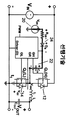
도 3a는 본 발명 회로의 제1 실시예를 나타내고, 도 3b는 제1 실시예의 특정 세부사항을 나타내며, 도 3c 내지 도 3e는 여러 시간 주기 동안의 전류 경로를 나타내고, 도 3e는 상기 회로의 타이밍 다이어그램이다.
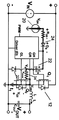
도 4a는 턴-온 다이오드를 갖는 본 발명 회로의 제2 실시예를 나타내고, 도 4b 내지 도 4d는 여러 시간 주기에서의 전류 경로를 나타내며, 도 4e는 선택적인 턴-온 저항의 추가를 보여준다.
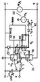
도 5는 제2 션트 다이오드를 갖는 본 발명 회로의 제3 실시예를 나타낸다.
도 6은 본 발명이 더 높은 수의 레벨을 갖는 컨버터로 확장된 제4 실시예를 나타낸다.
도 7a는 션트 다이오드로 대체된 션트 트랜지스터를 갖는 본 발명 회로의 제5 실시예를 나타내고, 도 7b는 제5 실시예의 특정 세부사항을 나타낸다.Other features and advantages of the present invention will become apparent when the following description is read in connection with the drawings.
1A shows a conventional buck converter bootstrap circuit for driving an e-mode GaN transistor arranged in a half bridge, FIGS. 1B to 1D show current paths through the circuit in several time periods, and FIG. 1E is the circuit. Is the timing diagram.
FIG. 2 shows a gate-to-source waveform of a GaN-based design with the conventional bootstrapping circuit of FIG. 1A.
Fig. 3a shows a first embodiment of the inventive circuit, Fig. 3b shows specific details of the first embodiment, Figs. 3c to 3e show the current path for several time periods, and Fig. 3e is the timing of the circuit It's a diagram.
Fig. 4a shows a second embodiment of the inventive circuit with a turn-on diode, Figs. 4b-4d show the current paths in several time periods, and Fig. 4e shows the addition of an optional turn-on resistor.
5 shows a third embodiment of the inventive circuit with a second shunt diode.
6 shows a fourth embodiment in which the invention is extended to a converter with a higher number of levels.
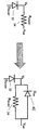
Fig. 7a shows a fifth embodiment of the circuit of the present invention with a shunt transistor replaced by a shunt diode, and Fig. 7b shows specific details of the fifth embodiment.
다음의 상세한 설명에서, 본 발명의 예시적인 실시예가 참조된다. 예시적인 실시예들은 당업자가 이들을 실시할 수 있도록 충분히 상세하게 설명된다. 다른 실시예가 채용될 수 있고 본 발명의 범위 및 사상을 벗어나지 않고 다양한 변경이 이루어질 수 있음을 이해해야 한다.In the following detailed description, reference is made to exemplary embodiments of the present invention. Exemplary embodiments are described in sufficient detail to enable any person skilled in the art to practice them. It should be understood that other embodiments may be employed and various changes may be made without departing from the scope and spirit of the present invention.
도 3a를 참조하면, 본 발명의 회로는 션트 저항 RSHUNT(34)에 의해 전력 회로로부터 분리되고(노드 GR/VSW), 그 캐소드에서 노드 VB에 연결되어, 데드-타임 충전 주기 t2 동안 부트스트랩 커패시터 CB(22)를 충전하기 위한 저전압 강하 경로를 제공한다. 션트 레지스터 RSHUNT(34)는 션트 다이오드 DSHUNT(32)를 통해 전류를 제어하고 제한한다.3A, the circuit of the present invention is separated from the power circuit by a shunt resistor R SHUNT 34 (node GR/V SW ), and connected to node V B at its cathode, during the dead-time charging period t2. Provides a low voltage drop path for charging the bootstrap capacitor C B (22). The shunt resistor R SHUNT (34) controls and limits the current through the shunt diode D SHUNT (32).
바람직하게는, 하이사이드 GaN 트랜지스터 Q1(12)의 소스는 게이트 구동 리턴(GR)에 직접 연결되어, 하이사이드 GaN 트랜지스터 Q1(12)의 턴-오프 정류(commutation)를 위한 턴-오프 저항을 제거한다. Preferably, the source of the high-side GaN transistor Q1 (12) is directly connected to the gate drive return (GR), eliminating the turn-off resistance for turn-off commutation of the high-side GaN transistor Q1 (12). do.
션트 다이오드 DSHUNT(32)는 부트스트랩 다이오드 DB(24)와 유사하거나 동일한 특성을 갖도록 설계/선택되어 구동 전압 VDR에 가장 가까운 부트스트랩 커패시터 전압 VCB를 제공할 수 있다. 선택적으로, 션트 다이오드 DSHUNT(32)는 부트스트랩 다이오드 DB(24)와 상이한 특성을 갖도록 설계/선택되어 구동 전압 VDR 이상 및/또는 이하의 전압을 생성할 수 있다. 션트 다이오드 DSHUNT(32)는 기존의 또는 쇼트키(Schottky) 다이오드로 구현될 수 있지만, VIN을 지원하는 전압 캐퍼빌리티를 가져야 한다. The
도 3c를 참조하면, 도 3a의 회로의 동작에 있어서, 주기 t1 동안, 종래 기술에서와 같이, 전력 트랜지스터 Q2는 드라이브-온(driven on) 되어 낮은 임피던스 및 전압 강하를 가지며, 부트스트랩 커패시터 충전 경로는 Q2를 통과하며, 이는 션트 다이오드 DSHUNT(32)를 차단하여 션트 네트워크를 비활성화시킨다. 도 3d에 도시된 바와 같이, 주기 t2 동안, 전력 트랜지스터 Q1 및 Q2는 드라이브-오프(driven off) 되고, Q2는 높은 전압 강하를 가지며, 이는 션트 다이오드 DSHUNT(32)를 도통시켜 션트 네트워크를 활성화시킨다. 따라서 부트스트랩 커패시터 충전 경로는 Q2를 통과하는 대신 션트 다이오드 DSHUNT(32)를 통과한다. 도 3e에 도시된 바와 같이, 주기 t3 동안, 전력 트랜지스터 Q1는 부트스트랩 커패시터에 의해 드라이브-온 되고 DSHUNT 네트워크는 비활성화된다.3C, in the operation of the circuit of FIG. 3A, during period t1, as in the prior art, power transistor Q2 is driven on to have a low impedance and voltage drop, and a bootstrap capacitor charging path Passes through Q2, which blocks the shunt diode D SHUNT (32), deactivating the shunt network. 3D, during period t2, power transistors Q1 and Q2 are driven off, Q2 has a high voltage drop, which conducts shunt diode D SHUNT 32 to activate the shunt network. Let it. So, instead of going through Q2, the bootstrap capacitor charging path goes through the shunt diode D SHUNT (32). As shown in Fig. 3e, during period t3, the power transistor Q1 is driven on by the bootstrap capacitor and the D SHUNT network is deactivated.
본 발명의 회로는 여러 가지 이유로 전술한 종래 기술의 회로보다 유리하다. 첫째, 션트 다이오드 DSHUNT(32)는 전술한 종래 기술의 회로에서와 같이 쇼트키 다이오드일 필요가 없으며, 이는 본 발명이 더 많은 종류의 애플리케이션에 적합하도록 만든다. 둘째로, 게이트 저항을 갖는 전술한 종래 기술의 회로에서는 이루어지지 않는, 전력 회로로부터 션트 저항 RSHUNT(34)을 분리하는 것은, RSHUNT가 독립적으로 설계될 수 있도록 하여 턴-오프 정류에 영향을 주지 않으면서 DSHUNT에 의해 처리되는 전류를 최적화할 수 있고, 이는 전력 스테이지 성능을 향상시킨다. 본 발명은 전술한 액티브 클램핑 스위치 및 동기식 부트스트랩 회로보다 훨씬 간단하다. 마지막으로, 션트 다이오드(32)는 소산적(dissipative)이지 않기 때문에, 본 발명은 전술한 종래 기술의 제너 다이오드 솔루션보다도 훨씬 우수한 성능을 나타낸다.The circuit of the present invention is advantageous over the circuit of the prior art described above for various reasons. First, the
도 3a에 도시된 본 발명의 회로의 단점은, 션트 저항 RSHUNT(34)이 턴-온 저항으로서 동작하여, 로우사이드 트랜지스터 Q1의 턴-온 정류에 영향을 미치는 것이다. 따라서, 도 4a에 도시된 본 발명의 제2 실시예에서, 도 3a의 실시예의 턴-온 속도를 개선하기 위해, Q1의 턴-온을 위한 역병렬(antiparallel) 턴-온 다이오드(40)(DON)가 제공된다. 제2 실시예에서, t2 데드-타임 주기 동안(도 4c에 도시된), RSHUNT 브랜치는 션트 다이오드 DSHUNT(32)를 통해 전도된 전류를 제어하고 부트스트랩 커패시터 충전을 제한한다. 도 4d에 도시된 것처럼, t3 턴-온 주기 동안, DON 브랜치는 활성화되어, 낮은 임피던스 경로를 제공하여 트랜지스터 Q1의 턴-온 속도를 향상시킨다. 바람직하게도, 도 4a의 제2 실시예는 Q1의 턴-온 또는 턴-오프 경로에서 저항을 갖지 않으므로, RSHUNT/DSHUNT 네트워크를 이용하여 부트스트랩 커패시터 과전압을 관리하면서 전력 디바이스의 최상의 스위칭 성능을 제공한다. 따라서, 도 3a에 도시된 제1 실시예와는 달리, 도 4a의 제2 실시예에서는, 션트 저항(34)이 하이사이드 트랜지스터 Q1의 전력 스위칭에 영향을 미치지 않는다. 선택적으로는, 도 4e에 도시된 것처럼, 턴-온 저항을 제공하기 위해 직렬 저항 RON(42)이 추가될 수 있다.A disadvantage of the circuit of the present invention shown in Fig. 3A is that the
도 5에 도시된 본 발명의 제3 실시예에서, 제2 션트 다이오드 DSHUNT2(52)는 션트 저항(RSHUNT)과 직렬로 삽입되어 유효 임피던스(effective impedance) 및 전압 강하에 대한 추가적인 제어를 제공할 수 있다.In the third embodiment of the present invention shown in Figure 5, the second shunt diode D SHUNT 2 (52) is inserted in series with the shunt resistor (R SHUNT ) to provide additional control for the effective impedance and voltage drop. Can provide.
도 6에 도시된 제4 실시예에서, 본 발명은 더 높은 레벨의 컨버터로 확장된다. 도 6에는 본 발명의 제1 실시예의 구현이 도시되었지만, 여기서 설명된 본 발명의 다른 실시예들 또한 유사한 방식으로 더 높은 수의 레벨을 갖는 컨버터로 확장될 수 있다.In the fourth embodiment shown in Fig. 6, the invention is extended to a higher level converter. Although the implementation of the first embodiment of the present invention is shown in Fig. 6, other embodiments of the present invention described herein can also be extended to converters with a higher number of levels in a similar manner.
도 7a 및 도 7b에 도시된 본 발명의 제5 실시예에서, 션트 다이오드 DSHUNT(32)는 능동(active) 반도체, 즉 트랜지스터 Q1(12)의 상보 게이트 구동 신호로 구동되는 트랜지스터 QSHUNT(70)로 대체될 수 있다. 미국 특허 제8,536,847호에는 부트스트랩 구동 회로에서 유사한 방식으로 트랜지스터(Q3)가 사용되는 회로가 개시되어 있지만, 이 특허의 회로는 전원 핀(power pin) 및 게이트 구동 핀(gate drive pin)이 상이한 전위를 기준으로 하기 때문에 복잡한 레퍼런스 전압 회로(reference voltage circuit)를 필요로 한다. 동일한 전위를 기준으로 하면, 더 작은 Q3에서 전원 전류가 전도되지 않도록 제한하는 밸런싱 방법이 없을 것이다. 이에 비해, 본 발명에서는, 션트 저항 RSHUNT(34)은 간단히 트랜지스터 QSHUNT(70)와 로우사이드 트랜지스터 Q2(14) 사이의 충전 비율을 제어하기 위해 임피던스를 제공하며, 이들은 모두 GND를 기준으로 하고, 이는 기준 전압 회로를 요구하지 않으면서 전원 핀과 게이트 구동 핀이 직접 연결되도록 허용한다.In the fifth embodiment of the present invention shown in Figs. 7A and 7B, the
전술한 여러 실시예들에서, 본 발명의 회로는 개별적으로(discretely) 또는 모놀리식으로 완전히 통합되어 단일 집적 회로로 구현될 수 있다. 상기 회로의 다양한 다이오드는 능동 스위치로 구현될 수 있다. 또한, 본 발명의 게이트 구동 회로는 전력 디바이스 및 수동 소자와 함께 칩 내에 집적될 수 있다. In the various embodiments described above, the circuits of the present invention may be implemented discretely or monolithically and completely integrated into a single integrated circuit. Various diodes of the circuit can be implemented as active switches. Further, the gate driving circuit of the present invention can be integrated in a chip together with a power device and a passive element.
상기 설명과 도면은 본 명세서에 설명된 특징 및 이점을 달성하는 특정 실시예를 설명하기 위한 것으로 간주된다. 특정 회로에 대한 변경 및 대체는 당업자에게 자명할 것이다. 따라서, 본 발명의 실시예는 전술한 설명과 도면에 의해 제한되는 것으로 간주되지 않는다.The above description and drawings are considered to be illustrative of specific embodiments that achieve the features and advantages described herein. Changes and substitutions for specific circuits will be apparent to those skilled in the art. Accordingly, embodiments of the present invention are not considered to be limited by the foregoing description and drawings.
Claims (15)
각각 소스, 드레인 및 게이트를 가지는 하이사이드 트랜지스터 및 로우사이드 트랜지스터 -상기 하이사이드 트랜지스터의 소스는 제1 노드에서 상기 로우사이드 트랜지스터의 드레인에 전기적으로 연결됨-;
상기 하이사이드 트랜지스터의 게이트에 전기적으로 결합된 게이트 드라이버;
상기 게이트 드라이버와 전기적으로 병렬로 결합된 부트스트랩(bootstrap) 커패시터;
캐노드 및 애노드를 가지는 션트 다이오드 -상기 션트 다이오드의 캐소드는 제2 노드에서 상기 커패시터에 연결되고, 상기 션트 다이오드의 애노드는 접지에 연결되고, 상기 션트 다이오드는 저전압 강하 경로를 제공하여 상기 부트스트랩 커패시터를 충전함-; 및
상기 션트 다이오드를 상기 제1 노드로부터 분리하고, 상기 션트 다이오드를 통하는 전류를 제어 및 제한하기 위해, 상기 제1 노드 및 제2 노드 사이에 전기적으로 연결된 션트 레지스터를 포함하는, 하프 브리지 토폴로지로 배열된 전기 회로.
As an electrical circuit arranged in a half bridge topology,
A high-side transistor and a low-side transistor each having a source, a drain, and a gate, wherein a source of the high-side transistor is electrically connected to a drain of the low-side transistor at a first node;
A gate driver electrically coupled to the gate of the high-side transistor;
A bootstrap capacitor electrically coupled in parallel with the gate driver;
Shunt diode having a cathode and an anode-The cathode of the shunt diode is connected to the capacitor at a second node, the anode of the shunt diode is connected to ground, and the shunt diode provides a low voltage drop path to the bootstrap capacitor. To charge -; And
Arranged in a half-bridge topology, comprising a shunt resistor electrically connected between the first node and the second node to separate the shunt diode from the first node and to control and limit the current through the shunt diode. Electrical circuit.
상기 하이사이드 및 로우사이드 트랜지스터는 인핸스먼트(enhancement) 모드 GaN 트랜지스터인 것을 특징으로 하는 전기 회로.
The method of claim 1,
Wherein the high-side and low-side transistors are enhancement mode GaN transistors.
상기 션트 레지스터와 전기적으로 역병렬(anti-parallel)로 연결된 턴-온 다이오드를 더 포함하는 것을 특징으로 하는 전기 회로.
The method of claim 1,
And a turn-on diode electrically connected to the shunt resistor in anti-parallel.
상기 턴-온 다이오드와 직렬로 연결된 턴-온 레지스터를 더 포함하는 것을 특징으로 하는 전기 회로.
The method of claim 3,
And a turn-on resistor connected in series with the turn-on diode.
제2 션트 다이오드를 더 포함하고, 상기 제2 션트 다이오드는 상기 션트 레지스터와 직렬로 연결되는 것을 특징으로 하는 전기 회로.
The method of claim 3,
The electric circuit further comprising a second shunt diode, wherein the second shunt diode is connected in series with the shunt resistor.
추가적인 하이사이드 트랜지스터들의 소스에 각각 연결된 추가적인 션트 다이오드들 및 션트 레지스터들을 더 포함하는 것을 특징으로 하는 전기 회로.
The method of claim 1,
The electrical circuit further comprising additional shunt diodes and shunt resistors each connected to a source of additional high side transistors.
상기 션트 다이오드는 션트 트랜지스터로 대체되고, 상기 션트 트랜지스터는 상기 로우사이드 트랜지스터의 게이트에 인가된 신호에 상보적인(complementary) 게이트 구동 신호로 구동되는 것을 특징으로 하는 전기 회로.
The method of claim 1,
Wherein the shunt diode is replaced by a shunt transistor, and the shunt transistor is driven with a gate driving signal complementary to a signal applied to a gate of the low-side transistor.
상기 게이트 드라이버, 상기 부트스트랩 커패시터, 상기 션트 다이오드 및 상기 션트 레지스터는 모두 모놀리식으로(monolithically) 단일 집적 회로에 집적되는 것을 특징으로 하는 전기 회로.
The method of claim 1,
Wherein the gate driver, the bootstrap capacitor, the shunt diode and the shunt resistor are all monolithically integrated into a single integrated circuit.
상기 집적 회로는 상기 하이사이드 및 로우사이드 트랜지스터들과 상기 회로의 수동 소자들을 포함하는 것을 특징으로 하는 전기 회로.
The method of claim 8,
Wherein the integrated circuit includes the high-side and low-side transistors and passive elements of the circuit.
상기 전기 회로의 하프 브리지는 각각 소스, 드레인 및 게이터를 갖는 하이사이드 트랜지스터 및 로우사이드 트랜지스터를 포함하고, 상기 하이사이드 트랜지스터의 소스는 제1 노드에서 상기 로우사이드 트랜지스터의 드레인에 전기적으로 연결되고, 상기 전기 회로는 상기 하이사이드 트랜지스터의 게이트에 전기적으로 결합된 게이트 드라이버, 상기 게이트 드라이버와 전기적으로 병렬(parallel)로 연결된 부트스트랩 커패시터를 더 포함하고,
상기 방법은 상기 하이사이드 및 로우사이드 트랜지스터가 모두 오프(off)일 때, 상기 로우사이드 트랜지스터와 전기적으로 병렬로 연결된 션트 네트워크를 통해, 상기 부트스트랩 커패시터를 충전하는 단계를 포함하며, 상기 션트 네트워크는 상기 로우사이드 트랜지스터의 역전압 강하와 비교하여 저전압 강하 충전 경로를 제공하며,
상기 션트 네트워크는,
캐노드 및 애노드를 가지는 션트 다이오드 -상기 션트 다이오드의 캐소드는 제2 노드에서 상기 커패시터에 연결되고, 상기 션트 다이오드의 애노드는 접지에 연결됨-, 및
상기 션트 다이오드를 상기 제1 노드로부터 분리하고, 상기 션트 다이오드를 통해 전류를 제어 및 제한하기 위해, 상기 제1 노드 및 제2 노드 사이에 전기적으로 연결된 션트 레지스터를 포함하는, 하프 브리지 구성으로 배열된 전기 회로에서 게이트 구동 과전압을 피하는 방법.
As a method of avoiding gate drive overvoltage in an electric circuit arranged in a half-bridge configuration,
The half bridge of the electric circuit includes a high-side transistor and a low-side transistor each having a source, a drain, and a gate, and a source of the high-side transistor is electrically connected to a drain of the low-side transistor at a first node, and the The electric circuit further includes a gate driver electrically coupled to the gate of the high side transistor, and a bootstrap capacitor electrically coupled to the gate driver in parallel,
The method includes charging the bootstrap capacitor through a shunt network electrically connected in parallel with the low-side transistor when both the high-side and low-side transistors are off, the shunt network Compared with the reverse voltage drop of the low-side transistor, a low voltage drop charging path is provided,
The shunt network,
A shunt diode having a cathode and an anode, the cathode of the shunt diode is connected to the capacitor at a second node, and the anode of the shunt diode is connected to ground, and
Arranged in a half-bridge configuration, comprising a shunt resistor electrically connected between the first node and the second node to separate the shunt diode from the first node and control and limit current through the shunt diode. How to avoid gate drive overvoltage in electrical circuits.
상기 하이사이드 및 로우사이드 트랜지스터는 인핸스먼트(enhancement) 모드 GaN 트랜지스터인 것을 특징으로 하는 방법.
The method of claim 10,
Wherein the high-side and low-side transistors are enhancement mode GaN transistors.
상기 션트 네트워크는 상기 션트 레지스터와 전기적으로 역병렬(anti-parallel)로 연결된 턴-온 다이오드를 더 포함하는 것을 특징으로 하는 방법.
The method of claim 10,
The shunt network further comprises a turn-on diode electrically connected to the shunt resistor in anti-parallel.
상기 션트 네트워크는 상기 턴-온 다이오드와 직렬로 연결된 턴-온 레지스터를 더 포함하는 것을 특징으로 하는 방법.
The method of claim 12,
Wherein the shunt network further comprises a turn-on resistor connected in series with the turn-on diode.
제2 션트 다이오드를 더 포함하고, 상기 제2 션트 다이오드는 상기 션트 레지스터와 직렬로 배치되는 것을 특징으로 하는 방법.
The method of claim 13,
And a second shunt diode, wherein the second shunt diode is disposed in series with the shunt resistor.
상기 션트 다이오드는 션트 트랜지스터로 대체되고, 상기 션트 트랜지스터는 상기 로우사이드 트랜지스터의 게이트에 인가된 신호에 상보적인(complementary) 게이트 구동 신호로 구동되는 것을 특징으로 하는 방법.The method of claim 10,
Wherein the shunt diode is replaced by a shunt transistor, and the shunt transistor is driven with a gate driving signal complementary to a signal applied to a gate of the low-side transistor.
Applications Claiming Priority (3)
| Application Number | Priority Date | Filing Date | Title |
|---|---|---|---|
| US201662428854P | 2016-12-01 | 2016-12-01 | |
| US62/428,854 | 2016-12-01 | ||
| PCT/US2017/063442 WO2018102299A1 (en) | 2016-12-01 | 2017-11-28 | Bootstrap capacitor over-voltage management circuit for gan transistor based power converters |
Publications (2)
| Publication Number | Publication Date |
|---|---|
| KR20190089200A KR20190089200A (en) | 2019-07-30 |
| KR102236287B1 true KR102236287B1 (en) | 2021-04-07 |
Family
ID=62241923
Family Applications (1)
| Application Number | Title | Priority Date | Filing Date |
|---|---|---|---|
| KR1020197018715A Active KR102236287B1 (en) | 2016-12-01 | 2017-11-28 | Bootstrap Capacitor Overvoltage Management Circuit for GaN Transistor-Based Power Converters |
Country Status (7)
| Country | Link |
|---|---|
| US (1) | US10454472B2 (en) |
| JP (1) | JP6839280B2 (en) |
| KR (1) | KR102236287B1 (en) |
| CN (1) | CN110024290B (en) |
| DE (1) | DE112017006120B4 (en) |
| TW (1) | TWI655835B (en) |
| WO (1) | WO2018102299A1 (en) |
Families Citing this family (29)
| Publication number | Priority date | Publication date | Assignee | Title |
|---|---|---|---|---|
| US8827889B2 (en) | 2012-05-21 | 2014-09-09 | University Of Washington Through Its Center For Commercialization | Method and system for powering implantable devices |
| US9960620B2 (en) | 2014-09-16 | 2018-05-01 | Navitas Semiconductor, Inc. | Bootstrap capacitor charging circuit for GaN devices |
| JP6819256B2 (en) * | 2016-12-07 | 2021-01-27 | 富士電機株式会社 | A drive circuit and a semiconductor module including the circuit |
| US10644601B2 (en) * | 2018-06-22 | 2020-05-05 | Taiwan Semiconductor Manufacturing Co., Ltd. | Dead-time conduction loss reduction for buck power converters |
| CN110635687B (en) * | 2018-06-22 | 2021-02-02 | 台湾积体电路制造股份有限公司 | Buck converter circuit and buck conversion method |
| CN112425057A (en) * | 2018-07-19 | 2021-02-26 | 三菱电机株式会社 | Power conversion device, motor drive device, and air conditioner |
| TWI732280B (en) * | 2018-08-28 | 2021-07-01 | 美商高效電源轉換公司 | CASCADED BOOTSTRAPPING GaN POWER SWITCH AND DRIVER |
| US10574229B1 (en) | 2019-01-23 | 2020-02-25 | Tagore Technology, Inc. | System and device for high-side supply |
| CN109873626B (en) * | 2019-03-27 | 2024-10-29 | 重庆瑜欣平瑞电子股份有限公司 | An IGBT negative voltage shutdown circuit |
| US11258444B2 (en) * | 2019-05-17 | 2022-02-22 | Schneider Electric It Corporation | Devices and methods for high-efficiency power switching with cascode GaN |
| DE102019207981A1 (en) * | 2019-05-31 | 2020-12-03 | Robert Bosch Gmbh | Circuit arrangement with at least one half bridge |
| CN110661427B (en) * | 2019-09-27 | 2020-07-24 | 浙江大学 | Digital control device of active clamp flyback AC-DC converter based on GaN device |
| EP3806333A1 (en) * | 2019-10-08 | 2021-04-14 | Delta Electronics, Inc. | Gate-driving circuit |
| WO2021079611A1 (en) | 2019-10-23 | 2021-04-29 | ローム株式会社 | Laser diode drive circuit |
| CN110824322B (en) * | 2019-10-30 | 2022-02-15 | 英诺赛科(珠海)科技有限公司 | Apparatus and method for measuring high electron mobility transistors |
| JP7308137B2 (en) * | 2019-12-03 | 2023-07-13 | ローム株式会社 | Gate drive and control circuits for switching circuits, switching power supplies |
| CN115280655A (en) * | 2020-04-06 | 2022-11-01 | 罗姆股份有限公司 | Switching circuit, switching power supply, gate driver circuit of switching power supply, and control circuit of switching power supply |
| CN111865149B (en) * | 2020-09-07 | 2022-04-05 | 珠海格力电器股份有限公司 | Motor control circuit and brushless direct current motor |
| CN113054962B (en) * | 2021-03-25 | 2024-03-19 | 苏州华太电子技术股份有限公司 | Co-source co-grid GaN power device and half-bridge application circuit thereof |
| US11973063B2 (en) | 2021-07-19 | 2024-04-30 | Infineon Technologies Ag | Semiconductor package with low parasitic connection to passive device |
| TWI780918B (en) * | 2021-09-17 | 2022-10-11 | 國立陽明交通大學 | Synchronous buck converter using a single gate driver control |
| US12212310B2 (en) * | 2021-10-12 | 2025-01-28 | Tagore Technology, Inc. | Gate bias circuit for a driver monolithically integrated with a GAN power FET |
| CN114400994B (en) * | 2022-01-10 | 2024-06-14 | 宁波正洋汽车部件有限公司 | NMOS high-side switch control circuit and method based on capacitor bootstrap boost |
| KR20230133004A (en) * | 2022-03-10 | 2023-09-19 | 현대자동차주식회사 | Laser driver for driving vcsel |
| JPWO2023228635A1 (en) * | 2022-05-25 | 2023-11-30 | ||
| CN116054572B (en) * | 2023-01-29 | 2025-06-24 | 苏州浪潮智能科技有限公司 | Control circuit of Buck power supply circuit |
| DE102024210682A1 (en) | 2024-11-07 | 2026-05-07 | Robert Bosch Gesellschaft mit beschränkter Haftung | Device and method for adaptive control of dead time in a half-bridge circuit |
| CN119675423B (en) * | 2024-12-02 | 2025-11-14 | 河南嘉晨智能控制股份有限公司 | A high-side MOS driving circuit |
| CN119652083B (en) * | 2024-12-05 | 2025-11-07 | 苏州大学 | Gallium nitride half-bridge type driving circuit |
Citations (1)
| Publication number | Priority date | Publication date | Assignee | Title |
|---|---|---|---|---|
| US20030151447A1 (en) | 2000-07-25 | 2003-08-14 | Stmicroelectronics S.R.L. | Bootstrap circuit in DC/DC static converters |
Family Cites Families (21)
| Publication number | Priority date | Publication date | Assignee | Title |
|---|---|---|---|---|
| US4760282A (en) * | 1986-11-13 | 1988-07-26 | National Semiconductor Corporation | High-speed, bootstrap driver circuit |
| US5408150A (en) * | 1992-06-04 | 1995-04-18 | Linear Technology Corporation | Circuit for driving two power mosfets in a half-bridge configuration |
| JP2601505Y2 (en) * | 1993-04-30 | 1999-11-22 | 株式会社島津製作所 | Bridge inverter circuit |
| US5373435A (en) * | 1993-05-07 | 1994-12-13 | Philips Electronics North America Corporation | High voltage integrated circuit driver for half-bridge circuit employing a bootstrap diode emulator |
| SG66453A1 (en) * | 1997-04-23 | 1999-07-20 | Int Rectifier Corp | Resistor in series with bootstrap diode for monolithic gate device |
| US20030015144A1 (en) * | 2001-06-18 | 2003-01-23 | Harold Bennett | Push-through pet food container and dispenser |
| WO2008114455A1 (en) * | 2007-03-21 | 2008-09-25 | Fujitsu Microelectronics Limited | Switching capacity generation circuit |
| US20080290841A1 (en) * | 2007-05-23 | 2008-11-27 | Richtek Technology Corporation | Charging Circuit for Bootstrap Capacitor and Integrated Driver Circuit Using Same |
| JP5191711B2 (en) * | 2007-09-05 | 2013-05-08 | 株式会社ジャパンディスプレイイースト | Liquid crystal display |
| JP5071248B2 (en) * | 2008-06-03 | 2012-11-14 | 住友電気工業株式会社 | Laser diode drive circuit |
| CA2767457C (en) * | 2009-09-10 | 2016-03-29 | E Craftsmen Associates Ltd. | Bootstrap startup and assist circuit |
| WO2011100971A2 (en) * | 2010-02-18 | 2011-08-25 | Danfoss Drives A/S | Method for implementing bootstrap-supply charging in a motor controller at energized motor and motor controller using such a method |
| US9136836B2 (en) | 2011-03-21 | 2015-09-15 | Semiconductor Components Industries, Llc | Converter including a bootstrap circuit and method |
| JP2013062717A (en) | 2011-09-14 | 2013-04-04 | Mitsubishi Electric Corp | Semiconductor device |
| US8593211B2 (en) * | 2012-03-16 | 2013-11-26 | Texas Instruments Incorporated | System and apparatus for driver circuit for protection of gates of GaN FETs |
| US8619445B1 (en) | 2013-03-15 | 2013-12-31 | Arctic Sand Technologies, Inc. | Protection of switched capacitor power converter |
| JP5991939B2 (en) * | 2013-03-25 | 2016-09-14 | 三菱電機株式会社 | Semiconductor device driving circuit and semiconductor device driving apparatus |
| JP6252388B2 (en) * | 2014-07-11 | 2017-12-27 | スズキ株式会社 | Engine valve gear |
| US9960620B2 (en) * | 2014-09-16 | 2018-05-01 | Navitas Semiconductor, Inc. | Bootstrap capacitor charging circuit for GaN devices |
| US9667245B2 (en) * | 2014-10-10 | 2017-05-30 | Efficient Power Conversion Corporation | High voltage zero QRR bootstrap supply |
| CN204244063U (en) * | 2014-10-24 | 2015-04-01 | 意法半导体研发(深圳)有限公司 | Anti-phase buck-boost type inverter drive circuit |
-
2017
- 2017-11-28 KR KR1020197018715A patent/KR102236287B1/en active Active
- 2017-11-28 WO PCT/US2017/063442 patent/WO2018102299A1/en not_active Ceased
- 2017-11-28 DE DE112017006120.2T patent/DE112017006120B4/en active Active
- 2017-11-28 CN CN201780073908.7A patent/CN110024290B/en active Active
- 2017-11-28 US US15/824,275 patent/US10454472B2/en active Active
- 2017-11-28 JP JP2019528691A patent/JP6839280B2/en active Active
- 2017-11-30 TW TW106141834A patent/TWI655835B/en active
Patent Citations (1)
| Publication number | Priority date | Publication date | Assignee | Title |
|---|---|---|---|---|
| US20030151447A1 (en) | 2000-07-25 | 2003-08-14 | Stmicroelectronics S.R.L. | Bootstrap circuit in DC/DC static converters |
Also Published As
| Publication number | Publication date |
|---|---|
| WO2018102299A1 (en) | 2018-06-07 |
| CN110024290B (en) | 2021-04-13 |
| JP6839280B2 (en) | 2021-03-03 |
| JP2019537417A (en) | 2019-12-19 |
| DE112017006120T5 (en) | 2019-09-05 |
| TWI655835B (en) | 2019-04-01 |
| TW201826677A (en) | 2018-07-16 |
| US20180159529A1 (en) | 2018-06-07 |
| CN110024290A (en) | 2019-07-16 |
| US10454472B2 (en) | 2019-10-22 |
| DE112017006120B4 (en) | 2020-12-10 |
| KR20190089200A (en) | 2019-07-30 |
Similar Documents
| Publication | Publication Date | Title |
|---|---|---|
| KR102236287B1 (en) | Bootstrap Capacitor Overvoltage Management Circuit for GaN Transistor-Based Power Converters | |
| KR102812897B1 (en) | INTEGRATED FAILSAFE PULLDOWN CIRCUIT FOR GaN SWITCH | |
| US8253398B2 (en) | Semiconductor device | |
| US9741702B2 (en) | Semiconductor power modules and devices | |
| JP6314073B2 (en) | Method and circuit for operating a circuit | |
| US10475909B2 (en) | Electric assembly including a bipolar switching device and a wide bandgap transistor | |
| CN104158536B (en) | Circuit with multiple bipolar transistors and the method for controlling the circuit | |
| IL95438A (en) | Switching circuit | |
| US20080068868A1 (en) | Power MESFET Rectifier | |
| JP6988256B2 (en) | Power converter | |
| CN115411711A (en) | Normally-off power switch with integrated fail-safe pull-down circuit and controllable turn-off time | |
| US20220345124A1 (en) | Efficient Switching Circuit | |
| US10186859B2 (en) | Reverse current protection for a switching unit | |
| US9219412B2 (en) | Buck converter with reverse current protection, and a photovoltaic system | |
| JP5832845B2 (en) | Semiconductor module and power conversion module | |
| US20240421810A1 (en) | Adaptive ringing clamp | |
| US12231042B2 (en) | Isolation connections for high-voltage power stage |
Legal Events
| Date | Code | Title | Description |
|---|---|---|---|
| PA0105 | International application |
Patent event date: 20190627 Patent event code: PA01051R01D Comment text: International Patent Application |
|
| PG1501 | Laying open of application | ||
| A201 | Request for examination | ||
| A302 | Request for accelerated examination | ||
| PA0201 | Request for examination |
Patent event code: PA02012R01D Patent event date: 20201102 Comment text: Request for Examination of Application |
|
| PA0302 | Request for accelerated examination |
Patent event date: 20201102 Patent event code: PA03022R01D Comment text: Request for Accelerated Examination |
|
| E902 | Notification of reason for refusal | ||
| PE0902 | Notice of grounds for rejection |
Comment text: Notification of reason for refusal Patent event date: 20201120 Patent event code: PE09021S01D |
|
| E701 | Decision to grant or registration of patent right | ||
| PE0701 | Decision of registration |
Patent event code: PE07011S01D Comment text: Decision to Grant Registration Patent event date: 20210128 |
|
| GRNT | Written decision to grant | ||
| PR0701 | Registration of establishment |
Comment text: Registration of Establishment Patent event date: 20210330 Patent event code: PR07011E01D |
|
| PR1002 | Payment of registration fee |
Payment date: 20210331 End annual number: 3 Start annual number: 1 |
|
| PG1601 | Publication of registration | ||
| PR1001 | Payment of annual fee |
Payment date: 20240304 Start annual number: 4 End annual number: 4 |
|
| PR1001 | Payment of annual fee |
Payment date: 20250217 Start annual number: 5 End annual number: 5 |