KR101865754B1 - Semiconductor device and method for fabricating the device - Google Patents
Semiconductor device and method for fabricating the device Download PDFInfo
- Publication number
- KR101865754B1 KR101865754B1 KR1020110065545A KR20110065545A KR101865754B1 KR 101865754 B1 KR101865754 B1 KR 101865754B1 KR 1020110065545 A KR1020110065545 A KR 1020110065545A KR 20110065545 A KR20110065545 A KR 20110065545A KR 101865754 B1 KR101865754 B1 KR 101865754B1
- Authority
- KR
- South Korea
- Prior art keywords
- region
- layer
- channel
- forming
- stress generating
- Prior art date
- Legal status (The legal status is an assumption and is not a legal conclusion. Google has not performed a legal analysis and makes no representation as to the accuracy of the status listed.)
- Active
Links
Images


Classifications
-
- H—ELECTRICITY
- H10—SEMICONDUCTOR DEVICES; ELECTRIC SOLID-STATE DEVICES NOT OTHERWISE PROVIDED FOR
- H10D—INORGANIC ELECTRIC SEMICONDUCTOR DEVICES
- H10D84/00—Integrated devices formed in or on semiconductor substrates that comprise only semiconducting layers, e.g. on Si wafers or on GaAs-on-Si wafers
- H10D84/01—Manufacture or treatment
- H10D84/0123—Integrating together multiple components covered by H10D12/00 or H10D30/00, e.g. integrating multiple IGBTs
- H10D84/0126—Integrating together multiple components covered by H10D12/00 or H10D30/00, e.g. integrating multiple IGBTs the components including insulated gates, e.g. IGFETs
- H10D84/0165—Integrating together multiple components covered by H10D12/00 or H10D30/00, e.g. integrating multiple IGBTs the components including insulated gates, e.g. IGFETs the components including complementary IGFETs, e.g. CMOS devices
- H10D84/0167—Manufacturing their channels
-
- H—ELECTRICITY
- H10—SEMICONDUCTOR DEVICES; ELECTRIC SOLID-STATE DEVICES NOT OTHERWISE PROVIDED FOR
- H10D—INORGANIC ELECTRIC SEMICONDUCTOR DEVICES
- H10D30/00—Field-effect transistors [FET]
- H10D30/01—Manufacture or treatment
- H10D30/021—Manufacture or treatment of FETs having insulated gates [IGFET]
- H10D30/027—Manufacture or treatment of FETs having insulated gates [IGFET] of lateral single-gate IGFETs
- H10D30/0278—Manufacture or treatment of FETs having insulated gates [IGFET] of lateral single-gate IGFETs forming single crystalline channels on wafers after forming insulating device isolations
-
- H—ELECTRICITY
- H10—SEMICONDUCTOR DEVICES; ELECTRIC SOLID-STATE DEVICES NOT OTHERWISE PROVIDED FOR
- H10D—INORGANIC ELECTRIC SEMICONDUCTOR DEVICES
- H10D30/00—Field-effect transistors [FET]
- H10D30/01—Manufacture or treatment
- H10D30/021—Manufacture or treatment of FETs having insulated gates [IGFET]
- H10D30/028—Manufacture or treatment of FETs having insulated gates [IGFET] of double-diffused metal oxide semiconductor [DMOS] FETs
- H10D30/0291—Manufacture or treatment of FETs having insulated gates [IGFET] of double-diffused metal oxide semiconductor [DMOS] FETs of vertical DMOS [VDMOS] FETs
-
- H—ELECTRICITY
- H10—SEMICONDUCTOR DEVICES; ELECTRIC SOLID-STATE DEVICES NOT OTHERWISE PROVIDED FOR
- H10D—INORGANIC ELECTRIC SEMICONDUCTOR DEVICES
- H10D30/00—Field-effect transistors [FET]
- H10D30/60—Insulated-gate field-effect transistors [IGFET]
-
- H—ELECTRICITY
- H10—SEMICONDUCTOR DEVICES; ELECTRIC SOLID-STATE DEVICES NOT OTHERWISE PROVIDED FOR
- H10D—INORGANIC ELECTRIC SEMICONDUCTOR DEVICES
- H10D30/00—Field-effect transistors [FET]
- H10D30/60—Insulated-gate field-effect transistors [IGFET]
- H10D30/791—Arrangements for exerting mechanical stress on the crystal lattice of the channel regions
- H10D30/797—Arrangements for exerting mechanical stress on the crystal lattice of the channel regions being in source or drain regions, e.g. SiGe source or drain
-
- H—ELECTRICITY
- H10—SEMICONDUCTOR DEVICES; ELECTRIC SOLID-STATE DEVICES NOT OTHERWISE PROVIDED FOR
- H10D—INORGANIC ELECTRIC SEMICONDUCTOR DEVICES
- H10D62/00—Semiconductor bodies, or regions thereof, of devices having potential barriers
- H10D62/80—Semiconductor bodies, or regions thereof, of devices having potential barriers characterised by the materials
- H10D62/82—Heterojunctions
- H10D62/822—Heterojunctions comprising only Group IV materials heterojunctions, e.g. Si/Ge heterojunctions
-
- H—ELECTRICITY
- H10—SEMICONDUCTOR DEVICES; ELECTRIC SOLID-STATE DEVICES NOT OTHERWISE PROVIDED FOR
- H10D—INORGANIC ELECTRIC SEMICONDUCTOR DEVICES
- H10D62/00—Semiconductor bodies, or regions thereof, of devices having potential barriers
- H10D62/80—Semiconductor bodies, or regions thereof, of devices having potential barriers characterised by the materials
- H10D62/83—Semiconductor bodies, or regions thereof, of devices having potential barriers characterised by the materials being Group IV materials, e.g. B-doped Si or undoped Ge
- H10D62/832—Semiconductor bodies, or regions thereof, of devices having potential barriers characterised by the materials being Group IV materials, e.g. B-doped Si or undoped Ge being Group IV materials comprising two or more elements, e.g. SiGe
- H10D62/8325—Silicon carbide
-
- H—ELECTRICITY
- H10—SEMICONDUCTOR DEVICES; ELECTRIC SOLID-STATE DEVICES NOT OTHERWISE PROVIDED FOR
- H10D—INORGANIC ELECTRIC SEMICONDUCTOR DEVICES
- H10D64/00—Electrodes of devices having potential barriers
- H10D64/01—Manufacture or treatment
- H10D64/017—Manufacture or treatment using dummy gates in processes wherein at least parts of the final gates are self-aligned to the dummy gates, i.e. replacement gate processes
-
- H—ELECTRICITY
- H10—SEMICONDUCTOR DEVICES; ELECTRIC SOLID-STATE DEVICES NOT OTHERWISE PROVIDED FOR
- H10D—INORGANIC ELECTRIC SEMICONDUCTOR DEVICES
- H10D64/00—Electrodes of devices having potential barriers
- H10D64/01—Manufacture or treatment
- H10D64/025—Manufacture or treatment forming recessed gates, e.g. by using local oxidation
- H10D64/027—Manufacture or treatment forming recessed gates, e.g. by using local oxidation by etching at gate locations
-
- H—ELECTRICITY
- H10—SEMICONDUCTOR DEVICES; ELECTRIC SOLID-STATE DEVICES NOT OTHERWISE PROVIDED FOR
- H10D—INORGANIC ELECTRIC SEMICONDUCTOR DEVICES
- H10D84/00—Integrated devices formed in or on semiconductor substrates that comprise only semiconducting layers, e.g. on Si wafers or on GaAs-on-Si wafers
- H10D84/01—Manufacture or treatment
- H10D84/0123—Integrating together multiple components covered by H10D12/00 or H10D30/00, e.g. integrating multiple IGBTs
- H10D84/0126—Integrating together multiple components covered by H10D12/00 or H10D30/00, e.g. integrating multiple IGBTs the components including insulated gates, e.g. IGFETs
- H10D84/0165—Integrating together multiple components covered by H10D12/00 or H10D30/00, e.g. integrating multiple IGBTs the components including insulated gates, e.g. IGFETs the components including complementary IGFETs, e.g. CMOS devices
- H10D84/017—Manufacturing their source or drain regions, e.g. silicided source or drain regions
-
- H—ELECTRICITY
- H10—SEMICONDUCTOR DEVICES; ELECTRIC SOLID-STATE DEVICES NOT OTHERWISE PROVIDED FOR
- H10D—INORGANIC ELECTRIC SEMICONDUCTOR DEVICES
- H10D84/00—Integrated devices formed in or on semiconductor substrates that comprise only semiconducting layers, e.g. on Si wafers or on GaAs-on-Si wafers
- H10D84/01—Manufacture or treatment
- H10D84/02—Manufacture or treatment characterised by using material-based technologies
- H10D84/03—Manufacture or treatment characterised by using material-based technologies using Group IV technology, e.g. silicon technology or silicon-carbide [SiC] technology
- H10D84/038—Manufacture or treatment characterised by using material-based technologies using Group IV technology, e.g. silicon technology or silicon-carbide [SiC] technology using silicon technology, e.g. SiGe
Landscapes
- Insulated Gate Type Field-Effect Transistor (AREA)
- Chemical & Material Sciences (AREA)
- Crystallography & Structural Chemistry (AREA)
- Electrodes Of Semiconductors (AREA)
Abstract
반도체 장치의 제조 방법이 제공된다. 반도체 기판과, 반도체 기판 상에 에피택셜 성장을 통해 형성된 프리 에피층(pre-epitaxial layer)을 제공하고, 프리 에피층 상에 더미 게이트 및 층간 절연막을 형성하고, 더미 게이트 및 더미 게이트 하부의 프리 에피층을 제거하여 서로 이격된 소오스 에피층 및 드레인 에피층을 형성하고, 소오스 에피층 및 드레인 에피층 사이에 선택 에피택셜 성장(selective epitaxial growth)을 통해 채널 에피층을 형성하고, 채널 에피층 상에 게이트 전극을 형성하는 것을 포함한다.A method of manufacturing a semiconductor device is provided. A semiconductor device comprising: a semiconductor substrate; and a pre-epitaxial layer formed through epitaxial growth on the semiconductor substrate, wherein a dummy gate and an interlayer insulating film are formed on the pre-epi layer, Layer is removed to form a source epitaxial layer and a drain epitaxial layer spaced apart from each other, a channel epitaxial growth is formed between the source epitaxial layer and the drain epitaxial layer by selective epitaxial growth, and a channel epitaxial layer is formed on the channel epitaxial layer Forming a gate electrode.
Description
본 발명은 반도체 장치 및 그 제조 방법에 관한 것이다.The present invention relates to a semiconductor device and a manufacturing method thereof.
고집적 반도체 장치를 제조하는데 있어서, 장치의 성능 향상을 위해 채널 내부에서 캐리어(carrier)의 이동도(mobility)를 증가시키는 방법이 연구되고 있다. 캐리어의 이동도를 증가시키는 방법으로는 예를 들어, 장치 내에 응력층을 형성하여 채널 영역을 인장(tensile) 또는 압축(compressive)시키는 방법을 들 수 있다.In the manufacture of highly integrated semiconductor devices, methods for increasing the mobility of carriers within the channel to improve the performance of the device have been studied. As a method of increasing the mobility of the carrier, for example, a method of forming a stress layer in the device to tensile or compress the channel region can be mentioned.
구체적으로, 전자가 주(major) 캐리어인 NMOS 영역은 인장 응력층을 형성하고 정공(hole)이 주 캐리어인 PMOS 영역은 압축 응력층을 형성할 수 있다. 또한, 응력 효과를 더욱 크게 하기 위하여 소오스 영역 및 드레인 영역을 예를 들어, 에피택셜 성장 공정 등을 통해 인장 응력층 또는 압축 응력층으로 형성할 수도 있다.Specifically, the NMOS region in which electrons are the major carriers forms a tensile stress layer and the PMOS region in which holes are the main carriers can form a compressive stress layer. In order to further increase the stress effect, the source region and the drain region may be formed as a tensile stress layer or a compressive stress layer through, for example, an epitaxial growth process or the like.
이 때, 에피택셜 성장 공정을 통해 형성되는 소오스 영역 및 드레인 영역에는 결정이 일 방향으로 고르게 성장되어 적층 결함(stacking fault) 등의 결함이 없어야 신뢰성 있는 반도체 장치의 제조가 가능하다.At this time, crystals are uniformly grown in one direction in the source region and the drain region formed through the epitaxial growth process, so that a reliable semiconductor device can be manufactured without any defects such as stacking faults.
또한, 소오스 영역 및 드레인 영역과 같은 응력층은 채널 영역에 최대한 응력을 주는 것이 좋으므로, 채널 영역의 표면과 가능한한 넓은 면적에서 맞닿도록 형성되어야 장치의 성능 향상으로 연결될 수 있다.In addition, since the stress layer such as the source region and the drain region is preferably stressed to the channel region as much as possible, it must be formed so as to be in contact with the surface of the channel region as wide as possible.
본 발명이 해결하고자 하는 기술적 과제는 성능이 향상된 반도체 장치를 제공하는 것이다.SUMMARY OF THE INVENTION It is an object of the present invention to provide a semiconductor device with improved performance.
본 발명이 해결하고자 하는 다른 기술적 과제는 성능이 향상된 반도체 장치를 제조할 수 있는 반도체 장치의 제조 방법을 제공하는 것이다.It is another object of the present invention to provide a method of manufacturing a semiconductor device capable of manufacturing a semiconductor device with improved performance.
본 발명의 기술적 과제들은 이상에서 언급한 기술적 과제로 제한되지 않으며, 언급되지 않은 또 다른 기술적 과제들은 아래의 기재로부터 당업자에게 명확하게 이해될 수 있을 것이다.The technical objects of the present invention are not limited to the technical matters mentioned above, and other technical subjects not mentioned can be clearly understood by those skilled in the art from the following description.
상기 기술적 과제를 달성하기 위한 본 발명의 일 실시예에 따른 반도체 장치는, 반도체 기판의 채널 영역 상에 형성된 채널 에피층(epitaxial layer), 채널 에피층 양측에 각각 형성된 소오스 에피층 및 드레인 에피층, 채널 에피층 상에 형성된 메탈 게이트 전극, 및 소오스 에피층 및 드레인 에피층 상에 형성된 층간 절연막을 포함한다.According to an aspect of the present invention, there is provided a semiconductor device including a channel epitaxial layer formed on a channel region of a semiconductor substrate, a source epitaxial layer and a drain epitaxial layer formed on both sides of the channel epitaxial layer, A metal gate electrode formed on the channel epi layer, and an interlayer insulating film formed on the source epi layer and the drain epi layer.
상기 기술적 과제를 달성하기 위한 본 발명의 다른 실시예에 따른 반도체 장치는, 제1 및 제2 영역을 포함하는 반도체 기판, 제1 영역 상에 형성된 제1 채널 에피층, 제1 채널 에피층 양 측에 각각 형성되되, 제1 채널 에피층 양 측면 전면에 걸쳐 압축 응력을 가하는 제1 소오스 및 드레인 에피층, 제2 영역 상에 형성된 제2 채널 에피층, 제2 채널 에피층 양 측에 각각 형성되되, 제2 채널 에피층 양 측면 전면에 걸쳐 인장 응력을 가하는 제2 소오스 및 드레인 에피층, 제1 및 제2 채널 에피층 상에 각각 형성된 제1 및 제2 메탈 게이트, 및 제1 소오스 및 드레인 에피층과 제2 소오스 및 드레인 에피층 상에 형성된 층간 절연막를 포함한다.According to another aspect of the present invention, there is provided a semiconductor device comprising: a semiconductor substrate including first and second regions; a first channel epitaxial layer formed on the first region; A first channel epitaxial layer formed on the second region, and a second channel epitaxial layer formed on both sides of the second channel epitaxial layer, each of the first channel epitaxial layer and the second channel epitaxial layer being formed on the first channel epitaxial layer and the second channel epitaxial layer, A second source and drain epitaxial layer that applies a tensile stress over both sides of the second channel epitaxial layer, first and second metal gates respectively formed on the first and second channel epitaxial layers, and first and second source and drain epitaxial layers, And an interlayer insulating film formed on the second source and drain epi layer.
상기 다른 기술적 과제를 달성하기 위한 본 발명의 일 실시예에 따른 반도체 장치의 제조 방법은, 반도체 기판과, 반도체 기판 상에 에피택셜 성장을 통해 형성된 프리 에피층(pre-epitaxial layer)을 제공하고, 프리 에피층 상에 더미 게이트 및 층간 절연막을 형성하고, 더미 게이트 및 더미 게이트 하부의 프리 에피층을 제거하여 서로 이격된 소오스 에피층 및 드레인 에피층을 형성하고, 소오스 에피층 및 드레인 에피층 사이에 선택 에피택셜 성장(selective epitaxial growth)을 통해 채널 에피층을 형성하고, 채널 에피층 상에 게이트 전극을 형성하는 것을 포함한다.According to another aspect of the present invention, there is provided a method of manufacturing a semiconductor device, including: providing a semiconductor substrate, a pre-epitaxial layer formed on the semiconductor substrate by epitaxial growth, Forming a dummy gate and an interlayer insulating film on the free epi layer, removing the free epi layer below the dummy gate and the dummy gate to form a source epitaxial layer and a drain epi layer spaced apart from each other, Forming a channel epitaxial layer through selective epitaxial growth, and forming a gate electrode on the channel epitaxial layer.
상기 다른 기술적 과제를 달성하기 위한 본 발명의 다른 실시예에 따른 반도체 장치의 제조 방법은, 반도체 기판 상에 더미 게이트를 형성하고, 반도체 기판 상에 에피택셜 성장을 통해 소오스 및 드레인 에피층을 형성하고, 소오스 및 드레인 에피층 상에 층간 절연막을 형성하고 이를 평탄화하여 더미 게이트를 노출시키고, 노출된 더미 게이트를 제거하여 반도체 기판의 상면 중 적어도 일부를 노출시키고, 노출된 반도체 기판의 상면 상에 선택 에피택셜 성장을 통해 채널 에피층을 형성하고, 채널 에피층 상에 게이트 전극을 형성하는 것을 포함한다.According to another aspect of the present invention, there is provided a method of fabricating a semiconductor device, comprising: forming a dummy gate on a semiconductor substrate; forming a source and drain epitaxial layer on the semiconductor substrate through epitaxial growth; , An interlayer insulating film is formed on the source and drain epitaxial layers and is planarized to expose the dummy gate, the exposed dummy gate is removed to expose at least a part of the upper surface of the semiconductor substrate, and a selective epitaxial Forming a channel epilayer through the facet growth, and forming a gate electrode on the channel epi layer.
상기 다른 기술적 과제를 달성하기 위한 본 발명의 또 다른 실시예에 따른 반도체 장치의 제조 방법은, 제1 및 제2 영역을 포함하는 반도체 기판과, 제1 영역 상에 에피택셜 성장을 통해 형성된 제1 프리 에피층과, 제2 영역 상에 애피택셜 성장을 통해 형성된 제2 프리 에피층을 제공하고, 제1 및 제2 프리 에피층 상에 각각 제1 및 제2 더미 게이트와 층간 절연막을 형성하고, 제1 및 제2 더미 게이트 및 제1 및 제2 더미 게이트 하부의 제1 및 제2 프리 에피층을 제거하여, 반도체 기판의 상면을 노출시키는 제1 및 제2 트렌치를 형성하고, 제1 및 제2 트렌치에 각각 선택 에피택셜 성장을 통해 제1 및 제2 채널 에피층을 형성하고, 제1 및 제2 채널 에피층 상에 각각 제1 및 제2 게이트 전극을 형성하는 것을 포함한다.According to another aspect of the present invention, there is provided a method of manufacturing a semiconductor device including a semiconductor substrate including first and second regions, a first region formed on the first region by epitaxial growth, Providing a free epi layer and a second free epi layer formed on the second region through epitaxial growth, forming first and second dummy gates and an interlayer insulating film on the first and second free epilayers respectively, The first and second dummy gates and the first and second free epilayers under the first and second dummy gates are removed to form first and second trenches exposing the upper surface of the semiconductor substrate, Forming a first and second channel epilayer through selective epitaxial growth on each of the two trenches, and forming first and second gate electrodes on the first and second channel epilayer, respectively.
상기 다른 기술적 과제를 달성하기 위한 본 발명의 또 다른 실시예에 따른 반도체 장치의 제조 방법은, PMOS 영역 및 NMOS 영역을 포함하는 반도체 기판과, PMOS 영역 상에 에피택셜 성장을 통해 형성된 실리콘 저마늄(SiGe) 에피층과, NMOS 영역 상에 에피택셜 성장을 통해 형성된 실리콘 카본(SiC) 에피층을 제공하고, 실리콘 저마늄 및 실리콘 카본 에피층 상에 각각 제1 및 제2 버퍼 산화막 패턴과 제1 및 제2 더미 게이트를 형성하고, 제1 및 제2 버퍼 산화막 패턴과 제1 및 제2 더미 게이트의 양 측에 각각 제1 및 제2 게이트 스페이서를 형성하고, 제1 및 제2 게이트 스페이서 사이의 제1 및 제2 더미 게이트, 제1 및 제2 버퍼 산화막 패턴, 실리콘 저마늄 에피층 및 실리콘 카본 에피층을 제거하여 반도체 기판의 상면을 노출시키는 제1 및 제2 트렌치를 형성하고, 제1 및 제2 트렌치에 각각 선택 에피택셜 성장을 통해 제1 및 제2 실리콘(Si) 채널 에피층을 형성하고, 제1 및 제2 실리콘(Si) 채널 에피층 상에 각각 제1 및 제2 게이트 스페이서의 측벽을 따라 연장되는 제1 및 제2 게이트 절연막을 형성하고, 제1 및 제2 게이트 절연막 상에 각각 제1 및 제2 메탈 게이트 전극을 형성하는 것을 포함한다.According to another aspect of the present invention, there is provided a method of manufacturing a semiconductor device including a semiconductor substrate including a PMOS region and an NMOS region, a silicon germanium layer formed through epitaxial growth on the PMOS region, SiGe) epitaxial layer formed on the NMOS region and a silicon carbon (SiC) epitaxial layer formed through epitaxial growth on the NMOS region, wherein the first and second buffer oxide film patterns are formed on the silicon germanium and silicon carbon epitaxial layers, First and second gate spacers are formed on both sides of the first and second buffer oxide film patterns and the first and second dummy gates, 1 and the second dummy gate, the first and second buffer oxide film patterns, the silicon germanium epilayer and the silicon carbon epi layer are removed to form first and second trenches exposing the upper surface of the semiconductor substrate, Forming a first and a second silicon (Si) channel epilayer through selective epitaxial growth on a second trench, respectively, and forming a first and a second silicon (Si) channel epitaxial layer on the first and second silicon Forming first and second gate insulating films extending along the sidewalls and forming first and second metal gate electrodes on the first and second gate insulating films, respectively.
기타 실시예들의 구체적인 사항들은 상세한 설명 및 도면들에 포함되어 있다.The details of other embodiments are included in the detailed description and drawings.
도 1은 본 발명의 일 실시예에 따른 반도체 장치의 단면도이다.
도 2 내지 도 7은 도 1에 도시된 반도체 장치의 제조 방법을 설명하기 위한 중간단계 도면들이다.
도 8은 본 발명의 다른 실시예에 따른 반도체 장치의 단면도이다.
도 9는 도 8에 도시된 반도체 장치의 제조 방법을 설명하기 위한 중간단계 도면이다.
도 10은 본 발명의 또 다른 실시예에 따른 반도체 장치의 단면도이다.
도 11 내지 도 18은 도 10에 도시된 반도체 장치의 제조 방법을 설명하기 위한 중간단계 도면들이다.
도 19는 본 발명의 또 다른 실시예에 따른 반도체 장치의 단면도이다.
도 20은 도 19에 도시된 반도체 장치의 제조 방법을 설명하기 위한 중간단계 도면이다.
도 21는 본 발명의 또 다른 실시예에 따른 반도체 장치의 단면도이다.
도 22는 도 21에 도시된 반도체 장치의 제조 방법을 설명하기 위한 중간단계 도면이다.1 is a cross-sectional view of a semiconductor device according to an embodiment of the present invention.
FIGS. 2 to 7 are intermediate steps for explaining a method of manufacturing the semiconductor device shown in FIG. 1. FIG.
8 is a cross-sectional view of a semiconductor device according to another embodiment of the present invention.
FIG. 9 is an intermediate step diagram for explaining the manufacturing method of the semiconductor device shown in FIG.
10 is a cross-sectional view of a semiconductor device according to another embodiment of the present invention.
FIGS. 11 to 18 are intermediate diagrams for explaining the manufacturing method of the semiconductor device shown in FIG.
19 is a cross-sectional view of a semiconductor device according to another embodiment of the present invention.
Fig. 20 is an intermediate step diagram for explaining a manufacturing method of the semiconductor device shown in Fig. 19;
21 is a cross-sectional view of a semiconductor device according to another embodiment of the present invention.
22 is an intermediate step diagram for explaining the manufacturing method of the semiconductor device shown in FIG.
본 발명의 이점 및 특징, 그리고 그것들을 달성하는 방법은 첨부되는 도면과 함께 상세하게 후술되어 있는 실시예들을 참조하면 명확해질 것이다. 그러나 본 발명은 이하에서 개시되는 실시예들에 한정되는 것이 아니라 서로 다른 다양한 형태로 구현될 것이며, 단지 본 실시예들은 본 발명의 개시가 완전하도록 하며, 본 발명이 속하는 기술분야에서 통상의 지식을 가진 자에게 발명의 범주를 완전하게 알려주기 위해 제공되는 것이며, 본 발명은 청구항의 범주에 의해 정의될 뿐이다. 도면에서 표시된 구성요소의 크기 및 상대적인 크기는 설명의 명료성을 위해 과장된 것일 수 있다. 명세서 전체에 걸쳐 동일 참조 부호는 동일 구성 요소를 지칭하며, "및/또는"은 언급된 아이템들의 각각 및 하나 이상의 모든 조합을 포함한다.BRIEF DESCRIPTION OF THE DRAWINGS The advantages and features of the present invention, and the manner of achieving them, will be apparent from and elucidated with reference to the embodiments described hereinafter in conjunction with the accompanying drawings. The present invention may, however, be embodied in many different forms and should not be construed as being limited to the embodiments set forth herein. Rather, these embodiments are provided so that this disclosure will be thorough and complete, and will fully convey the scope of the invention to those skilled in the art. Is provided to fully convey the scope of the invention to those skilled in the art, and the invention is only defined by the scope of the claims. The dimensions and relative sizes of the components shown in the figures may be exaggerated for clarity of description. Like reference numerals refer to like elements throughout the specification and "and / or" include each and every combination of one or more of the mentioned items.
소자(elements) 또는 층이 다른 소자 또는 층의 "위(on)" 또는 "상(on)"으로 지칭되는 것은 다른 소자 또는 층의 바로 위뿐만 아니라 중간에 다른 층 또는 다른 소자를 개재한 경우를 모두 포함한다. 반면, 소자가 "직접 위(directly on)" 또는 "바로 위"로 지칭되는 것은 중간에 다른 소자 또는 층을 개재하지 않은 것을 나타낸다.It is to be understood that when an element or layer is referred to as being "on" or " on "of another element or layer, All included. On the other hand, a device being referred to as "directly on" or "directly above " indicates that no other device or layer is interposed in between.
비록 제1, 제2 등이 다양한 소자나 구성요소들을 서술하기 위해서 사용되나, 이들 소자나 구성요소들은 이들 용어에 의해 제한되지 않음은 물론이다. 이들 용어들은 단지 하나의 소자나 구성요소를 다른 소자나 구성요소와 구별하기 위하여 사용하는 것이다. 따라서, 이하에서 언급되는 제1 소자나 구성요소는 본 발명의 기술적 사상 내에서 제2 소자나 구성요소 일 수도 있음은 물론이다.Although the first, second, etc. are used to describe various elements or components, it is needless to say that these elements or components are not limited by these terms. These terms are used only to distinguish one element or component from another. Therefore, it is needless to say that the first element or the constituent element mentioned below may be the second element or constituent element within the technical spirit of the present invention.
다른 정의가 없다면, 본 명세서에서 사용되는 모든 용어(기술 및 과학적 용어를 포함)는 본 발명이 속하는 기술분야에서 통상의 지식을 가진 자에게 공통적으로 이해될 수 있는 의미로 사용될 수 있을 것이다. 또 일반적으로 사용되는 사전에 정의되어 있는 용어들은 명백하게 특별히 정의되어 있지 않는 한 이상적으로 또는 과도하게 해석되지 않는다.Unless defined otherwise, all terms (including technical and scientific terms) used herein may be used in a sense commonly understood by one of ordinary skill in the art to which this invention belongs. Also, commonly used predefined terms are not ideally or excessively interpreted unless explicitly defined otherwise.
도 1은 본 발명의 일 실시예에 따른 반도체 장치의 단면도이다.1 is a cross-sectional view of a semiconductor device according to an embodiment of the present invention.
도 1을 참조하면, 반도체 장치는 반도체 기판(100), 채널 에피층(channel epitaxial layer)(120), 소오스 에피층(source epitaxial layer)(112), 드레인 에피층(drain epitaxial layer)(114), 게이트 전극(130), 및 층간 절연막(150)을 포함한다.1, a semiconductor device includes a
반도체 기판(100)은 예를 들어, 벌크(bulk) 실리콘 기판, 실리콘-온-인슐레이터(silicon on insulator: SOI) 기판, 게르마늄 기판, 게르마늄-온-인슐레이터(germanium on insulator: GOI) 기판, 실리콘-게르마늄 기판, 또는 선택 에피택셜 성장(SEG; Selective Epitaxial Growth)을 수행하여 획득한 에피택셜 박막의 기판일 수 있다.The
채널 에피층(120)은 반도체 기판(100)의 채널 영역(C) 상에 형성될 수 있다. 이러한 채널 에피층(120)은 선택 에피택셜 성장을 통해 형성될 수 있다.The
소오스 및 드레인 에피층(112, 114)은 채널 에피층(120)의 양 측에 각각 형성될 수 있다. 이러한 소오스 및 드레인 에피층(112, 114)은 채널 에피층(120)과 면 접촉하도록 형성될 수 있다. 구체적으로, 소오스 에피층(112)은 채널 에피층(120)과 제1 접촉면(J)을 통해 면 접촉할 수 있고, 드레인 에피층(114)은 채널 에피층(120)과 제2 접촉면(K)을 통해 면 접촉할 수 있다. 여기서, 소오스 및 드레인 에피층(112, 114)은 예를 들어, 불순물이 포함된 실리콘(Si) 에피층일 수 있고, 채널 에피층(120)은 실리콘(Si) 에피층일 수 있다. 구체적으로, 소오스 및 드레인 에피층(112, 114)은 저마늄(Ge) 또는 카본(C) 중 적어도 어느 하나를 포함하는 실리콘(Si) 에피층일 수 있고, 채널 에피층(120)은 불순물을 포함하지 않은 실리콘(Si) 에피층일 수 있다.The source and
만약, 소오스 및 드레인 에피층(112, 114)이 실리콘 저마늄(SiGe) 에피층일 경우, 채널 에피층(120)은 압축 응력(compressive stress)을 받을 수 있다. 따라서, 채널 에피층(120)의 주 캐리어가 정공(hole)일 경우, 캐리어의 이동도(mobility)가 향상될 수 있다.If the source and
특히, 본 실시예에서 소오스 및 드레인 에피층(112, 114)은 채널 에피층(120)과 채널 에피층(120)의 측면 전면에 걸쳐 면 접촉 하게 되므로, 채널 에피층(120)의 측면 전면에 걸쳐 고르게 압축 응력을 가할 수 있게 된다. 따라서, 소오스 및 드레인 에피층(112, 114)이 채널 에피층(120)에 점(point) 접촉하거나, 채널 에피층(120)의 측면 일부에 국소적으로 면 접촉하는 경우에 비해, 캐리어의 이동도를 크게 향상시킬 수 있게 된다. 따라서, 반도체 장치의 성능이 크게 향상되게 된다.Particularly, in this embodiment, since the source and
한편, 비록 도시하지는 않았지만, 소오스 및 드레인 에피층(112, 114)이 만약 실리콘 카본(SiC) 에피층일 경우, 채널 에피층(120)은 인장 응력(tensile stress)을 받을 수 있다. 채널 에피층(120)의 주 캐리어가 전자(electron)라면, 앞서 압축 응력의 경우와 마찬가지로 채널 에피층(120)의 측면 전면에 걸쳐 고르게 인장 응력을 가할 수 있기 때문에, 채널 에피층(120) 내 캐리어의 이동도를 크게 향상될 수 있다.On the other hand, although not shown, when the source and
본 실시예에 따른 소오스 및 드레인 에피층(112, 114)을 이루는 결정의 성장 방향은 일 방향으로 고르게 형성될 수 있다. 구체적으로, 소오스 및 드레인 에피층(112, 114)을 이루는 결정은 반도체 기판(100)에 수직인 방향(예를 들어, Y)으로 고르게 성장될 수 있다. 이는 소오스 및 드레인 에피층(112, 114)이 반도체 기판(100) 상에 예를 들어, Y방향으로 에피택셜 성장되어 형성되었기 때문일 수 있다.The crystal growth directions of the source and drain
한편, 도 1에서는 소오스 에피층(112)이 채널 에피층(120)의 좌측에 형성되고, 드레인 에피층(114)이 채널 에피층(120)의 우측에 형성된 것이 도시되어 있으나, 본 발명이 이에 제한되는 것은 아니다. 필요에 따라 소오스 에피층(112)과 채널 에피층(120)은 서로 위치를 바꿔 형성될 수 있다.1, the
게이트 전극(130)은 채널 에피층(120) 상에 형성될 수 있다. 특히, 본 실시예서 게이트 전극(130)은 예를 들어, 메탈(metal) 게이트 전극(130)일 수 있다. 이러한 게이트 전극(130)을 구성하는 메탈로는 예를 들어, 구리(Cu), 알루미늄(Al), 텅스텐(W), 타이타늄 나이트라이드(TiN) 등을 들 수 있으나, 본 발명에 이에 제한되는 것은 아니다.A
층간 절연막(150)은 소오스 및 드레인 에피층(112, 114) 상에 형성될 수 있다. 이러한 층간 절연막(150)은 예를 들어, 실리콘 나이트라이드(SiNx) 또는 실리콘 옥사이드(SiOx) 등의 물질로 이루어질 수 있으나, 본 발명이 이에 제한되는 것은 아니다.An interlayer insulating
이하, 도 1에 도시된 반도체 장치를 제조할 수 있는 예시적인 일 제조 방법에 대해 설명하도록 한다.Hereinafter, one exemplary manufacturing method capable of manufacturing the semiconductor device shown in Fig. 1 will be described.
도 2 내지 도 5는 도 1에 도시된 반도체 장치의 제조 방법을 설명하기 위한 중간단계 도면들이다.FIGS. 2 to 5 are intermediate steps for explaining the method of manufacturing the semiconductor device shown in FIG. 1. FIG.
도 2를 참조하면, 반도체 기판(100) 상에 에피택셜 성장(epitaxial growing)을 통해 프리 에피층(pre-epitaxial layer)(110)을 형성한다. 이러한 프리 에피층(110)은 저마늄(Ge) 또는 카본(C)등의 불순물이 포함된 실리콘(Si) 에피층일 수 있다.Referring to FIG. 2, a
다음 도 3을 참조하면, 프리 에피층(110) 상에 더미 게이트(120) 및 층간 절연막(150)을 형성한다. 더미 게이트(120)는 일반적으로 공지된 제조 방법을 통해 형성하는 것이 가능하다. 일 예로, 프리 에피층(110) 상에 예를 들어, 폴리 실리콘(poly-si) 등으로 이루어진 도전층(미도시)을 형성하고, 이를 패터닝(patterning)함으로써 더미 게이트(120)를 형성할 수 있다. 이러한 더미 게이트(120)는 폴리 실리콘(poly-si) 등의 도전 물질로 이루어질 수 있으나, 본 발명이 이에 제한되는 것은 아니다. 3, a
층간 절연막(150) 역시 일반적으로 공지된 제조 방법을 통해 형성하는 것이 가능하다. 일 예로, 더미 게이트(120)를 형성한 후, 프리 에피층(110) 및 더미 게이트(120) 상에 절연 물질(미도시)을 형성하고, 더미 게이트(120)의 상면이 노출될 때까지 절연 물질(미도시)을 평탄화하여 층간 절연막(150)을 형성할 수 있다.The
다음 도 4를 참조하면, 더미 게이트(도 3의 120) 및 더미 게이트(도 3의 120) 하부의 프리 에피층(110)을 제거하여, 서로 이격된 소오스 에피층(112) 및 드레인(114) 에피층을 형성한다. 이 때, 더미 게이트(도 3의 120) 및 더미 게이트(도 3의 120) 하부의 프리 에피층(110)을 제거하는 것은, 예를 들어, 반도체 기판(100)의 상면이 노출될 때까지, 더미 게이트(도 3의 120) 및 더미 게이트(도 3의 120) 하부의 프리 에피층(110)을 식각(etching)하는 것을 포함할 수 있다. 이 때, 더미 게이트(도 3의 120) 하부의 프리 에피층(110)은 반도체 기판(100)의 상면이 노출될 때까지 충분한 시간에 걸쳐 식각될 수 있다.4, the
다음 도 5를 참조하면, 소오스 에피층(112) 및 드레인 에피층(114) 사이에 선택 에피택셜 성장(SEG; Selective Epitaxial Growth)을 통해 채널 에피층(120)을 형성한다. 여기서 채널 에피층(120)은 예를 들어, 선택 에피택셜 성장을 통해 형성되는 실리콘(Si) 에피층일 수 있다. 그리고, 이 경우 채널 에피층(120)은 노출된 반도체 기판(100)의 상면 상에는 형성되나, 층간 절연막(150) 상에는 형성되지 않을 수 있다.5, a
만약, 소오스 에피층(112) 및 드레인 에피층(114)이 실리콘 저마늄(SiGe) 에피층이라면, 이러한 채널 에피층(120)은 양 측면에서 압축 응력을 받으며 Y 방향으로 에피택셜 성장될 수 있다. 또한, 비록 도시하지는 않았지만, 소오스 에피층(112) 및 드레인 에피층(114)이 실리콘 카본(SiC) 에피층이라면, 이러한 채널 에피층(120)은 양 측면에서 인장 응력을 받으며 예를 들어, Y 방향으로 에피택셜 성장될 수 있다.If the source
본 실시예에서는 이렇게 채널 에피층(120)이 양 측면 전면에 걸쳐 압축 응력 또는 인장 응력을 받으며 성장되므로, 최대한 넓은 접촉면에서 골고루 응력을 받는 채널 에피층(120)을 형성할 수 있게 된다.In this embodiment, the
또한, 본 실시예에서는 반도체 기판(100) 상에 일 방향(예를 들어, Y)으로 프리 에피층(110)을 에피택셜 성장을 통해 형성하고, 이를 패터닝하여 소오스 에피층(112)과 드레인 에피층(114)을 형성한다. 따라서, 소오스 에피층(112)과 드레인 에피층(114)을 이루는 결정의 성장 방향도 일 방향(예를 들어, Y)으로 고르게 성장되게 된다.In this embodiment, a
만약, 반도체 기판(100)에 트렌치(미도시) 등을 형성하고 이러한 트렌치(미도시)에 소오스 에피층(112)과 드레인 에피층(114)을 형성하게 되면, 트렌치(미도시)의 형상에 따라 여러 방향으로 결정이 성장되어 소오스 에피층(112)과 드레인 에피층(114)이 형성될 수 있다. 이 경우, 각 방향에서 성장해온 성장 결정은 일정 영역에서 서로 교차하게 되는데, 이 때 서로 교차하는 성장 결정의 격자 구조 차이로 인해 적층 결함(stacking fault)이 발생할 수 있다.If a trench (not shown) or the like is formed in the
하지만, 본 실시예의 경우, 소오스 에피층(112)과 드레인 에피층(114)을 이루는 결정의 성장 방향이 일 방향(예를 들어, Y)으로 고르게 성장되므로, 이러한 적층 결함이 발생되는 것을 사전에 예방할 수 있다. 따라서, 반도체 장치의 신뢰성을 높일 수 있으며, 나아가 반도체 장치의 성능을 향상시킬 수 있다.However, in the case of this embodiment, since the growth direction of the crystal constituting the source
다시 도 1을 참조하면, 채널 에피층(120) 상에 게이트 전극(130)을 형성한다. 이러한 게이트 전극(130)은 예를 들어, 층간 절연막(150) 사이의 채널 에피층(120) 상에 메탈을 채우고, 이를 평탄화함으로써 형성할 수 있다. 이에 관한 보다 구체적인 사항은 추후 보다 구체적으로 설명하도록 한다.Referring again to FIG. 1, a
한편, 도 1에 도시된 본 발명의 일 실시예에 따른 반도체 장치는 이와 다른 제조 방법을 통해 제조하는 것도 가능하다. 이하, 도 1에 도시된 반도체 장치를 제조할 수 있는 예시적인 다른 제조 방법에 대해 설명하도록 한다.Meanwhile, the semiconductor device according to an embodiment of the present invention shown in FIG. 1 may be manufactured by another manufacturing method. Hereinafter, another exemplary manufacturing method capable of manufacturing the semiconductor device shown in Fig. 1 will be described.
도 6 및 도 7은 도 1에 도시된 반도체 장치의 제조 방법을 설명하기 위한 중간단계 도면들이다.FIGS. 6 and 7 are intermediate diagrams for explaining the manufacturing method of the semiconductor device shown in FIG.
도 6을 참조하면, 반도체 기판(100) 상에 더미 게이트(121)를 형성한다. 이 때, 더미 게이트(121)는 예를 들어, 반도체 기판(100) 상에 절연층(미도시)을 형성하고 이를 패터닝함으로써 형성할 수 있다.Referring to FIG. 6, a
다음 도 7을 참조하면, 반도체 기판(100) 상에 에피택셜 성장을 통해 소오스 에피층(112) 및 드레인 에피층(114)을 형성한다. 이 때, 특히 소오스 에피층(112)과 드레인 에피층(114)은 선택 에피택셜 성장을 통해 더미 게이트(121) 양 측에 형성될 수 있다.7, a
예를 들어, 더미 게이트(121)를 실리콘 나이트라이드(SiNx) 또는 실리콘 옥사이드(SiOx)등의 절연 물질로 형성하고 선택 에피택셜 성장 공정을 수행하면, 더미 게이트(121) 상에는 에피층이 형성되지 않고, 반도체 기판(100) 상에는 에피택셜 성장이 일어나게 된다. 따라서, 도시된 것과 같이 더미 게이트(121) 양 측에 선택적으로 소오스 에피층(112)과 드레인 에피층(114)을 형성할 수 있다.For example, when the
한편, 도 7에는 선택 에피택셜 성장 공정을 통해 더미 게이트(121) 양 측에 선택적으로 소오스 에피층(112)과 드레인 에피층(114)이 형성된 것만 도시되어 있으나, 본 발명이 이에 제한되는 것은 아니다. 후술하겠지만, 더미 게이트(121)는 소오스 에피층(112)과 드레인 에피층(114) 형성 후 제거되므로, 더미 게이트(121) 상에 에피층이 형성되더라도 무방하다.In FIG. 7, only the source
이후, 소오스 에피층(112)과 드레인 에피층(114) 상에 층간 절연막(150)을 형성하고, 도 4에 도시된 것과 같이, 더미 게이트(도 7의 121)를 제거하여 반도체 기판(100)의 상면 중 적어도 일부(예를 들어, 채널 영역)를 노출시킨다. 그리고, 도 5에 도시된 것과 같이, 노출된 반도체 기판(100)의 상면 상에 선택 에피택셜 성장을 통해 채널 에피층(120)을 형성하고, 채널 에피층(120) 상에 게이트 전극(도 1의 130)을 형성하면 도 1에 도시된 반도체 장치를 제조할 수 있게 된다.An interlayer insulating
다음, 도 8 및 도 9를 참조하여 본 발명의 다른 실시예에 따른 반도체 장치 및 그 제조 방법에 대해 설명하도록 한다. 이하에서는 앞서 설명한 실시예들과 동일한 사항에 대해서는 중복된 설명을 생략하고, 그 차이점에 대해서만 설명하도록 한다.Next, a semiconductor device and a manufacturing method thereof according to another embodiment of the present invention will be described with reference to FIGS. 8 and 9. FIG. Hereinafter, duplicate descriptions will be omitted for the same elements as those of the above-described embodiments, and only differences will be described.
도 8은 본 발명의 다른 실시예에 따른 반도체 장치의 단면도이다. 도 9는 도 8에 도시된 반도체 장치의 제조 방법을 설명하기 위한 중간단계 도면이다.8 is a cross-sectional view of a semiconductor device according to another embodiment of the present invention. FIG. 9 is an intermediate step diagram for explaining the manufacturing method of the semiconductor device shown in FIG.
도 8을 참조하면, 반도체 장치의 채널 에피층(121)은 반도체 기판(100)의 채널 영역(C) 상에 형성되되, 반도체 기판(100)에 형성된 채널 트렌치(105) 내에 형성될 수 있다. 즉, 채널 에피층(121)의 하면은 소오스 에피층(112) 및 드레인 에피층(114)의 하면보다 낮게 형성될 수 있다.8, the
이렇게 형성된 채널 에피층(121)의 상부 영역은 측면 전면에 걸쳐 소오스 에피층(112) 및 드레인 에피층(114)으로부터 압축 응력(또는 인장 응력)을 받게 된다. 따라서, 채널 에피층(121)내의 케리어 이동도를 효과적으로 향상시킬 수 있다.The upper region of the
본 실시예에 따른 반도체 장치는 일반적으로 공지된 다양한 제조 방법을 통해 형성하는 것이 가능하다. 그 일 예로, 더미 게이트(도 3의 120) 하부의 프리 에피층(도 3의 110) 또는 더미 게이트(도 7의 121)를 오버 에치(over etch)하여 도 9에 도시된 것과 같이 반도체 기판(100)에 채널 트렌치(105)를 형성한 후, 채널 트렌치(105) 상에 채널 에피층(도 8의 121)을 애피택셜 성장시킴으로써 본 실시예에 따른 반도체 장치를 형성하는 것이 가능하다.The semiconductor device according to the present embodiment can be formed through various generally known manufacturing methods. As an example, overetching the pre-epi layer (110 in FIG. 3) or the dummy gate (121 in FIG. 7) under the dummy gate (120 in FIG. 3) It is possible to form the semiconductor device according to the present embodiment by forming the
다음 도 10을 참조하여, 본 발명의 또 다른 실시예에 따른 반도체 장치에 대해 설명한다. 이하에서도, 앞서 설명한 실시예들과 차이점을 중심으로 설명하도록 한다.Next, a semiconductor device according to still another embodiment of the present invention will be described with reference to FIG. Hereinafter, differences from the above-described embodiments will be mainly described.
도 10은 본 발명의 또 다른 실시예에 따른 반도체 장치의 단면도이다.10 is a cross-sectional view of a semiconductor device according to another embodiment of the present invention.
도 10을 참조하면, 반도체 장치는 반도체 기판(200), 제1 및 제2 채널 에피층(272, 274), 제1 및 제2 소오스 에피층(212A, 214A), 제1 및 제2 드레인 에피층(212B, 214B), 제1 및 제2 게이트 전극(292, 294), 층간 절연막(250)을 포함한다.10, a semiconductor device includes a
반도체 기판(200)은 제1 영역(I)과 제2 영역(II)을 포함할 수 있다. 본 실시예에서, 제1 영역(I)은 예를 들어, PMOS 소자가 형성되는 영역일 수 있고, 제2 영역(II)은 NMOS 소자가 형성되는 영역일 수 있다. 하지만, 본 발명이 이에 제한되는 것은 아니며, 제1 영역(I)과 제2 영역(II)에 형성되는 소자들은 얼마든지 변형될 수 있다. 즉, 도시되지는 않았으나, 제1 영역(I)에 NMOS 소자가 형성되고, 제2 영역(II)에 PMOS 소자가 형성되는 것도 가능하며, 제1 및 제2 영역(I, II)에 모두 NMOS 소자 또는 PMOS 소자가 형성되는 것도 가능하다.The
반도체 기판(200)에는 소자 분리막(202)이 형성될 수 있다. 이러한 소자 분리막(202)은 반도체 기판(100)에 형성된 트렌치에 매립된 절연막(STI; Shallow Trench Isolation)일 수 있으나, 본 발명이 이에 제한되는 것은 아니다.A
또한, 도 10에서는 소자 분리막(202)의 높이가 반도체 기판(200)의 상면과 동일한 것이 도시되어 있으나, 본 발명이 이에 제한되는 것은 아니다. 필요에 따라 소자 분리막(202)의 상면은 반도체 기판(200)의 상면보다 높게 형성될 수도 있고, 낮게 형성될 수도 있다.10, the height of the
제1 및 제2 채널 에피층(272, 274)은 반도체 기판(200)의 채널 영역(C) 상에 형성될 수 있다. 구체적으로, 제1 채널 에피층(272)은 반도체 기판(200)의 제1 영역(I)의 채널 영역 채널 영역(C) 상에 형성될 수 있고, 제2 채널 에피층(274)은 반도체 기판(200)의 제2 영역(II)의 채널 영역 채널 영역(C) 상에 형성될 수 있다.The first and
제1 채널 에피층(272) 양 측에는 제1 소오스 에피층(212A)과 제1 드레인 에피층(212B)이 형성될 수 있고, 제2 채널 에피층(274) 양 측에는 제2 소오스 에피층(214A)과 제2 드레인 에피층(214B)이 형성될 수 있다.A
이러한, 제1 및 제2 소오스 에피층(212A, 214A)과 제1 및 제2 드레인 에피층(212B, 214B)은 각각 제1 및 제2 채널 에피층(272, 274)) 양 측의 반도체 기판(200) 상에 형성될 수 있다. 구체적으로, 제1 및 제2 소오스 에피층(212A, 214A)과 제1 및 제2 드레인 에피층(212B, 214B)은 반도체 기판(200) 상에는 형성되나, 소자 분리막(202) 상에는 미형성될 수 있다.The first and
제1 및 제2 채널 에피층(272, 274) 상에는 각각 제1 및 제2 게이트 절연막(282, 284)이 형성될 수 있다. 이러한 제1 및 제2 게이트 절연막(282, 284)은 각각 제1 및 제2 게이트 스페이서(242, 244)의 측벽을 따라 연장된 형태로 형성될 수 있다.First and second
비록 상세히 도시하지는 않았지만, 본 실시예에서 제1 및 제2 게이트 절연막(282, 284)은 예를 들어, 각각 계면 산화막(interfacial oxide layer)(미도시)과 고유전율막(high-k oxide layer)(미도시)의 이중막 구조로 형성될 수 있다. 이러한 계면 산화막(미도시)을 이루는 물질로는 SiO2를 예로 들 수 있고, 고유전율막(미도시)을 이루는 물질로는 HfO2, Al2O3, ZrO2, TaO2 등을 예로 들 수 있으나, 본 발명이 이에 제한되는 것은 아니다.Although not shown in detail, in this embodiment, the first and second
제1 및 제2 게이트 절연막(282, 284) 상에는 각각 제1 및 제2 게이트 전극(292, 294)이 형성될 수 있다. 본 실시예에서, 제1 및 제2 게이트 전극(292, 294)은 메탈 게이트 전극일 수 있다.First and
제1 및 제2 게이트 전극(292, 294) 양 측(또는, 제1 및 제2 게이트 절연막(282, 284)의 양 측)에는 각각 제1 및 제2 게이트 스페이서(242, 244)가 형성될 수 있다. 이러한 제1 및 제2 게이트 스페이서(242, 244)는 예를 들어, 실리콘 나이트라이드(SiNx) 또는 실리콘 옥사이드(SiOx) 등의 절연 물질로 이루어질 수 있으나, 본 발명이 이에 제한되는 것은 아니다.First and
반도체 기판(200) 및 소자 분리막(202) 상에는 층간 절연막(250)이 형성될 수 있다. 이러한 층간 절연막(250)은 예를 들어, 실리콘 나이트라이드(SiNx) 등의 절연 물질로 이루어질 수 있으나, 본 발명이 이에 제한되는 것은 아니다.An interlayer insulating
본 실시예에 따른 반도체 장치는 PMOS 소자(예를 들어 PMOS 트랜지스터)가 형성된 제1 영역(I)의 제1 채널 에피층(272)이 양 측면 전면에 걸쳐 고르게 압축 응력을 받게 된다. 따라서, 제1 채널 에피층(272)의 주 캐리어인 정공의 이동도를 향상시킬 수 있다. 또한, NMOS 소자(예를 들어, NMOS 트랜지스터)가 형성된 제2 영역(II)의 제1 채널 에피층(272)은 양 측면 전면에 걸쳐 고르게 인장 응력을 받는다. 따라서, 제2 채널 에피층(274)의 주 캐리어인 전자의 이동도를 향상시킬 수 있다.In the semiconductor device according to the present embodiment, the first
이하, 도 10에 도시된 반도체 장치를 제조할 수 있는 예시적인 일 제조 방법에 대해 설명하도록 한다.Hereinafter, one exemplary manufacturing method capable of manufacturing the semiconductor device shown in Fig. 10 will be described.
도 11 내지 도 16은 도 10에 도시된 반도체 장치의 제조 방법을 설명하기 위한 중간단계 도면들이다.FIGS. 11 to 16 are intermediate diagrams for explaining the manufacturing method of the semiconductor device shown in FIG.
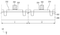
도 11을 참조하면, 반도체 기판(200)에 소자 분리막(202)을 형성한다. 구체적으로, 반도체 기판(200)의 제1 영역(I) 및 제2 영역(II) 각각에 트렌치를 형성하고, 트렌치에 절연막을 매립하여 소자 분리막(202)을 형성할 수 있다. 트렌치에 매립되는 절연막의 상면은 필요에 따라 반도체 기판(200)의 상면보다 높거나 낮게 형성할 수 있다.Referring to FIG. 11, an
다음 도 12를 참조하면, 반도체 기판(200) 상에 프리 에피층(212, 214)을 형성한다. 구체적으로, 반도체 기판(200)의 제1 영역(I) 상에 에피택셜 성장을 통해 제1 프리 에피층(212)을 형성하고, 제2 영역(II) 상에 에피택셜 성장을 통해 제2 프리 에피층(214)을 형성할 수 있다. Referring next to FIG. 12, a pre-epilayer 212, 214 is formed on a
이 때, 제1 및 제2 프리 에피층(212, 214)은 선택 에피택셜 성장을 통해 형성될 수 있다. 구체적으로, 반도체 기판(200) 상에서는 일 방향(예를 들어, Y)으로 결정이 성장하기 때문에 제1 및 제2 프리 에피층(212, 214)이 형성될 수 있으나, 소자 분리막(202) 상에서는 결정 성장이 일어나지 않기 때문에 소자 분리막(202) 상에는 제1 및 제2 프리 에피층(212, 214)이 미형성될 수 있다.At this time, the first and
여기서, 제1 프리 에피층(212)은 예를 들어, 제1 불순물을 포함하는 실리콘(Si) 에피층일 수 있고, 제2 프리 에피층(214)은 제1 불순물과 다른 제2 불순물을 포함하는 실리콘(Si) 에피층일 수 있다. 구체적으로, 제1 프리 에피층(212)은 예를 들어, 실리콘 저머늄(SiGe) 에피층일 수 있고, 제2 프리 에피층(214)은 실리콘 카본(SiC) 에피층일 수 있다.Here, the first
다음 도 13을 참조하면, 제1 및 제2 프리 에피층(212, 214) 상에 각각 제1 및 제2 버퍼 산화막 패턴(222, 224)과 제1 및 제2 더미 게이트(232, 234)를 형성한다. 제1 및 제2 버퍼 산화막 패턴(222, 224)과 제1 및 제2 더미 게이트(232, 234)는 일반적으로 공지된 다양한 제조 방법을 통해 형성하는 것이 가능하다. 그 일 예로, 제1 및 제2 프리 에피층(212, 214) 상에 버퍼 산화막(미도시) 및 도전층(미도시)을 순차적으로 적층하고, 순차적으로 적층된 버퍼 산화막(미도시)과 도전층(미도시)을 패터닝하여 도시된 제1 및 제2 버퍼 산화막 패턴(222, 224)과 제1 및 제2 더미 게이트(232, 234)를 형성할 수 있다. 이 때, 제1 및 제2 버퍼 산화막 패턴(222, 224)과 제1 및 제2 더미 게이트(232, 234)는 반도체 기판(200)의 채널 영역(도 10의 C) 상에 형성될 수 있다.Referring to FIG. 13, first and second buffer
다음 도 14를 참조하면, 제1 및 제2 버퍼 산화막 패턴(222, 224)과 제1 및 제2 더미 게이트(232, 234)의 양 측에 각각 제1 및 제2 게이트 스페이서(242, 244)를 형성한다. 제1 및 제2 게이트 스페이서(242, 244)는 예를 들어, 실리콘 나이트라이드(SiNx) 또는 실리콘 옥사이드(SiOx) 등의 절연 물질로 이루어질 수 있으나, 본 발명이 이에 제한되는 것은 아니다. 또한, 도면에는 제1 및 제2 게이트 스페이서(242, 244)가 반도체 기판(200)에 수직인 기둥 형상으로 형성된 것이 도시되어 있으나, 필요에 따라 제1 및 제2 게이트 스페이서(242, 244)의 형상은 L자형 등으로 얼마든지 변형될 수 있다.Referring to FIG. 14, first and
제1 및 제2 게이트 스페이서(242, 244)를 형성한 후, 반도체 기판(200) 상에 층간 절연막(250)을 형성한다. 이러한 층간 절연막(250)은 예를 들어, 실리콘 나이트라이드(SiNx) 등의 절연 물질을 반도체 기판(200) 상에 형성하고, 이를 제1 및 제2 더미 게이트(232, 234)의 상면이 노출될 때까지 평탄화하여 형성할 수 있다.After the first and
다음 도 15를 참조하면, 제1 및 제2 더미 게이트(도 14의 232, 234) 및 제1 및 제2 더미 게이트(도 14의 232, 234) 하부의 제1 및 제2 프리 에피층(도 14의 212, 214)을 제거하여, 반도체 기판(200)의 상면을 노출시키는 제1 및 제2 트렌치(262, 264)를 형성한다. Next, referring to FIG. 15, first and second pre-epi layers (also referred to as " first and second free layers ") of first and second dummy gates (232 and 234 in FIG. 14) and first and second dummy gates (232 and 234 in FIG. 14) 14 and 212 are removed to form first and
구체적으로, 제1 및 제2 게이트 스페이서(242, 244) 사이의 제1 및 제2 더미 게이트(도 14의 232, 234), 제1 및 제2 버퍼 산화막 패턴(도 14의 222, 224) 및, 제1 및 제2 프리 에피층(도 14의 212, 214)을 충분한 시간 동안 식각하여, 반도체 기판(200)의 상면을 노출시키는 제1 및 제2 트렌치(262, 264)를 형성할 수 있다.Specifically, the first and second dummy gates (232 and 234 in Fig. 14), the first and second buffer oxide film patterns (222 and 224 in Fig. 14) and the first and second dummy gates between the first and
이렇게 제1 및 제2 트렌치(262, 264)가 형성됨으로써, 제1 트렌치(262) 양 측에는 제1 소오스 에피층(212A)과 제1 드레인 에피층(212B)이 형성되고, 제2 트렌치(264) 양 측에는 제2 소오스 에피층(214A)과 제2 드레인 에피층(214B)이 형성될 수 있다.The first
다음 도 16을 참조하면, 제1 및 제2 트렌치(도 15의 262, 264)에 각각 선택 에피택셜 성장을 통해 예를 들어, 실리콘(Si)으로 이루어진 제1 및 제2 채널 에피층(272, 274)을 형성한다. 이렇게 선택 에피택셜 성장을 통해 제1 및 제2 채널 에피층(272, 274)을 형성하게 되면, 층간 절연막(250) 및 제1 및 제2 게이트 스페이서(242, 244) 상에서는 결정 성장이 일어나지 않고, 노출된 반도체 기판(200) 상에서 결정 성장이 일어나게 된다. 따라서, 제1 채널 에피층(272)은 제1 소오스 및 드레인 에피층(212A, 212B)에 의해 압축 응력을 받으며 반도체 기판(200) 상에 형성되게 되고, 제2 채널 에피층(274)은 제2 소오스 및 드레인 에피층(214A, 214B)에 의해 인장 응력을 받으며 반도체 기판(200) 상에 형성 되게 된다.Referring now to FIG. 16, first and
다음 도 10을 참조하면, 제1 및 제2 게이트 스페이서(242, 244) 사이의 제1 및 제2 채널 에피층(272, 274) 상에 각각 제1 및 제2 게이트 절연막(282, 284)을 형성한다. 여기서, 제1 및 제2 게이트 절연막(282, 284)은 제1 및 제2 게이트 스페이서(242, 244)의 측벽을 따라 연장되도록 형성될 수 있다.10, first and second
비록 상세히 도시하지는 않았지만, 제1 및 제2 게이트 절연막(282, 284)은 예를 들어, 각각 계면 산화막(interfacial oxide layer)(미도시)과 고유전율막(high-k oxide layer)(미도시)의 이중막 구조로 형성될 수 있다. 이러한 계면 산화막(미도시)을 이루는 물질로는 SiO2를 예로 들 수 있고, 고유전율막(미도시)을 이루는 물질로는 HfO2, Al2O3, ZrO2, TaO2 등을 예로 들 수 있으나, 본 발명이 이에 제한되는 것은 아니다.Although not shown in detail, the first and second
다시 도 10을 참조하면, 제1 및 제2 게이트 절연막(282, 284) 상에 각각 예를 들어, 알루미늄(Al), 구리(Cu) 텅스텐(W), 타이타늄 나이트라이드(TiN) 등의 메탈을 채우고, 이를 평탄화하여 제1 및 제2 게이트 전극(292, 294)을 형성한다. Referring again to FIG. 10, a metal such as aluminum (Al), copper (Cu) tungsten (W), or titanium nitride (TiN) is deposited on the first and second
본 실시예에서는 이러한 제1 및 제2 게이트 전극(292, 294)을 이루는 물질로 메탈을 예시하고 있지만, 본 발명이 이에 제한되는 것은 아니다.In this embodiment, metal is used as a material forming the first and
이와 같은 제조 방법을 통해 반도체 장치를 제조하게 되면, 제1 채널 에피층(272)이 양 측면 전면에 걸쳐 고르게 압축 응력을 받게 되고, 제2 채널 에피층(274)이 양 측면 전면에 걸쳐 고르게 인장 응력을 받게 된다. 따라서, 제1 채널 에피층(272)의 주 캐리어인 정공과 제2 채널 에피층(274)의 주 캐리어인 전자의 이동도를 크게 향상시킬 수 있다.When the semiconductor device is manufactured through such a manufacturing method, the
한편, 본 실시예에서는 제1 소오스 및 드레인 에피층(212A, 212B)과 제2 소오스 및 드레인 에피층(214A, 214B)이 각각 반도체 기판(200) 상에 직접 에피택셜 성장되어 형성되기 때문에, 제1 소오스 및 드레인 에피층(212A, 212B)과 제2 소오스 및 드레인 에피층(214A, 214B)을 이루는 결정의 성장 방향이 일 방향(예를 들어, Y)으로 고르게 성장되게 된다. 따라서, 제1 소오스 및 드레인 에피층(212A, 212B)과 제2 소오스 및 드레인 에피층(214A, 214B) 내에 적층 결함이 발생될 확률이 줄어들게 된다.Since the first source and drain epilayers 212A and 212B and the second source and drain epilayers 214A and 214B are formed by directly epitaxially growing on the
본 실시예에서는 반도체 기판(200)의 제1 영역(I)과 제2 영역(II)에 동시에 각각 PMOS 소자와 NMOS 소자를 형성하는 것을 설명하였으나, 본 발명이 이에 제한되는 것은 아니다. 필요에 따라 소자의 형성 순서는 얼마든지 변형될 수 있다. 즉 예를 들어, 반도체 기판(200)의 제1 영역(I)에 먼저 PMOS 소자를 형성하고, 그 이후에 제2 영역(II)에 NMOS 소자를 형성하는 것이 가능하며, 반대로 반도체 기판(200)의 제2 영역(II)에 먼저 NMOS 소자를 형성하고, 그 이후에 제1 영역(I)에 PMOS 소자를 형성하는 것도 가능하다. 또한, 본 실시예와 반대로 반도체 기판(200)의 제1 영역(I)에 NMOS 소자를 형성하고, 제2 영역(II)에 PMOS 소자를 형성하는 것 역시 가능하다.In this embodiment, the PMOS device and the NMOS device are simultaneously formed in the first region I and the second region II of the
이상에서는 도 10에 도시된 반도체 장치를 제조할 수 있는 예시적인 일 제조 방법에 대해 설명하였으나, 이러한 제조 방법은 얼마든지 변형이 가능하다. 이하, 도 10에 도시된 반도체 장치를 제조할 수 있는 예시적인 다른 제조 방법에 대해 설명하도록 한다.Although an exemplary manufacturing method capable of manufacturing the semiconductor device shown in FIG. 10 has been described above, any of these manufacturing methods can be modified. Hereinafter, another exemplary manufacturing method capable of manufacturing the semiconductor device shown in FIG. 10 will be described.
도 17 및 도 18은 도 10에 도시된 반도체 장치의 제조 방법을 설명하기 위한 중간단계 도면들이다.FIGS. 17 and 18 are intermediate diagrams for explaining the manufacturing method of the semiconductor device shown in FIG.
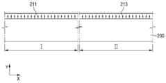
도 17을 참조하면, 반도체 기판(200) 상에 제1 및 제2 프리 에피층(211, 213)을 형성한다. 구체적으로, 반도체 기판(200)의 제1 영역(I) 전면에 걸쳐 에피택셜 성장을 통해 제1 프리 에피층(211)을 형성하고, 제2 영역(II) 전면에 걸쳐 에피택셜 성장을 통해 제2 프리 에피층(213)을 형성한다.Referring to FIG. 17, first and second
여기서, 제1 프리 에피층(211)은 예를 들어, 제1 불순물을 포함하는 실리콘(Si) 에피층일 수 있고, 제2 프리 에피층(213)은 제1 불순물과 다른 제2 불순물을 포함하는 실리콘(Si) 에피층일 수 있다. 구체적으로, 제1 프리 에피층(211)은 예를 들어, 실리콘 저머늄(SiGe) 에피층일 수 있고, 제2 프리 에피층(213)은 실리콘 카본(SiC) 에피층일 수 있다.Here, the first
다음 도 18을 참조하면, 제1 및 제2 프리 에피층(도 17의 211, 213)과 반도체 기판(200)을 패터닝하여, 반도체 기판(200)에 소자 분리 트렌치(미도시)를 형성한다. 그리고, 소자 분리 트렌치(미도시)를 절연막 등으로 매립하여 소자 분리막(202)을 형성한다.Referring to FIG. 18, device isolation trenches (not shown) are formed in the
이후, 도 13 내지 도 16에 도시된 앞선 실시예와 동일한 공정을 수행하게 되면 도 10에 도시된 반도체 장치를 제조할 수 있게 된다.13 to 16, the semiconductor device shown in FIG. 10 can be manufactured.
다음 도 19 및 도 20을 참조하여, 본 발명의 또 다른 실시예에 따른 반도체 장치 및 그 제조 방법에 대해 설명한다. 이하에서도, 앞서 설명한 실시예들과 차이점을 중심으로 설명하도록 한다.Next, a semiconductor device and a manufacturing method thereof according to still another embodiment of the present invention will be described with reference to FIGS. 19 and 20. FIG. Hereinafter, differences from the above-described embodiments will be mainly described.
도 19는 본 발명의 또 다른 실시예에 따른 반도체 장치의 단면도이다. 도 20은 도 19에 도시된 반도체 장치의 제조 방법을 설명하기 위한 중간단계 도면이다.19 is a cross-sectional view of a semiconductor device according to another embodiment of the present invention. Fig. 20 is an intermediate step diagram for explaining a manufacturing method of the semiconductor device shown in Fig. 19;
도 19를 참조하면, 반도체 기판(200)의 제1 영역(I)에 형성된 제1 채널 에피층(272)은 반도체 기판(200)에 형성된 채널 트렌치(도 20의 205)에 형성될 수 있다. 따라서, 반도체 기판(200)의 제1 영역(I)에 형성된 제1 채널 에피층(272)의 하면(A)은 반도체 기판(200)의 제2 영역(II)에 형성된 제2 채널 에피층(274)의 하면(B)보다 낮게 형성될 수 있다.19, a
이와 같은 반도체 장치는 일반적으로 공지된 다양한 제조 방법을 통해 형성하는 것이 가능하다. 그 일 예로, 도 20을 참조하면, 제1 영역(I)에 형성된 제1 게이트 스페이서(242) 사이의 제1 프리 에피층(도 14의 212)을 식각할 시, 제1 프리 에피층(도 14의 212)을 오버 에치(over etch)하여 반도체 기판(200)에 채널 트렌치(205)를 형성한다. 그리고, 형성된 채널 트렌치(205)에 선택 에피택셜 성장을 통해 제1 채널 에피층(272)을 형성하면 제1 채널 에피층(272)의 하면(A)을 제2 채널 에피층(274)의 하면(B)보다 낮게 형성할 수 있다.Such a semiconductor device can be formed through various generally known manufacturing methods. 20, when etching the first free epilayer (212 in FIG. 14) between the
비록 도 19에는 제1 채널 에피층(272)의 하면(A)이 제2 채널 에피층(274)의 하면(B)보다 낮게 형성된 것만 도시되어 있으나, 본 발명이 이에 제한되는 것은 아니다. 필요에 따라, 제2 채널 에피층(274)의 하면(B)을 제1 채널 에피층(272)의 하면(A)보다 낮게 형성할 수 있음은 물론이다.Although the lower surface A of the
다음 도 21 및 도 22를 참조하여, 본 발명의 또 다른 실시예에 따른 반도체 장치 및 그 제조 방법에 대해 설명한다. 이하에서도, 앞서 설명한 실시예들과 차이점을 중심으로 설명하도록 한다.Next, a semiconductor device and a manufacturing method thereof according to still another embodiment of the present invention will be described with reference to FIGS. 21 and 22. FIG. Hereinafter, differences from the above-described embodiments will be mainly described.
도 21는 본 발명의 또 다른 실시예에 따른 반도체 장치의 단면도이다. 도 22는 도 21에 도시된 반도체 장치의 제조 방법을 설명하기 위한 중간단계 도면이다.21 is a cross-sectional view of a semiconductor device according to another embodiment of the present invention. 22 is an intermediate step diagram for explaining the manufacturing method of the semiconductor device shown in FIG.
도 21을 참조하면, 반도체 기판(200)의 제1 영역(I)에 형성된 제1 채널 에피층(273)의 상면(P)은 인접하는 제1 소오스 및 드레인 에피층(272A, 272B)의 상면보다 높게 형성될 수 있다. 또한, 반도체 기판(200)의 제1 영역(I)에 형성된 제1 채널 에피층(273)의 상면(P)은 제2 영역(II)에 형성된 제2 채널 에피층(274)의 상면(Q)보다 높게 형성될 수 있다.21, the upper surface P of the first
이와 같은 반도체 장치는 일반적으로 공지된 다양한 제조 방법을 통해 형성하는 것이 가능하다. 그 일 예로, 도 22를 참조하면, 제1 및 제2 트렌치(도 15의 262, 264)에 각각 선택 에피택셜 성장을 통해 제1 및 제2 채널 에피층(273, 274) 형성 시, 제1 채널 에피층(273)의 상면(P)을 인접하는 제1 소오스 및 드레인 에피층(272A, 272B)의 상면보다 높게 형성하거나, 제2 채널 에피층(274)의 상면(Q)보다 높게 형성함으로써 도 21에 도시된 반도체 장치를 제조할 수 있다.Such a semiconductor device can be formed through various generally known manufacturing methods. 22, when the first and
한편, 비록 도 21에는 제1 채널 에피층(273)의 상면(P)이 인접하는 제1 소오스 및 드레인 에피층(272A, 272B)의 상면보다 높게 형성된 것이 도시되어 있으나, 본 발명이 이에 제한되는 것은 아니다. 필요에 따라, 제2 채널 에피층(274)의 상면(Q)이 인접하는 제2 소오스 및 드레인 에피층(274A, 274B)의 상면보다 높게 형성될 수 있음은 물론이다. 또한, 도 21에는 제1 채널 에피층(273)의 상면(P)이 제2 채널 에피층(274)의 상면(Q)보다 높게 형성된 것이 도시되어 있으나, 반대로 제2 채널 에피층(274)의 상면(Q)을 제1 채널 에피층(273)의 상면(P)보다 높게 형성할 수 있음도 물론이다. 즉, 도시되지 않은 다양한 실시예의 조합이 가능하다.21, the upper surface P of the
이상 첨부된 도면을 참조하여 본 발명의 실시예들을 설명하였으나, 본 발명은 상기 실시예들에 한정되는 것이 아니라 서로 다른 다양한 형태로 제조될 수 있으며, 본 발명이 속하는 기술분야에서 통상의 지식을 가진 자는 본 발명의 기술적 사상이나 필수적인 특징을 변경하지 않고서 다른 구체적인 형태로 실시될 수 있다는 것을 이해할 수 있을 것이다. 그러므로 이상에서 기술한 실시예들은 모든 면에서 예시적인 것이며 한정적이 아닌 것으로 이해해야만 한다.While the present invention has been described in connection with what is presently considered to be practical exemplary embodiments, it is to be understood that the invention is not limited to the disclosed embodiments, but, on the contrary, It is to be understood that the invention may be embodied in other specific forms without departing from the spirit or essential characteristics thereof. It is therefore to be understood that the above-described embodiments are illustrative in all aspects and not restrictive.
100, 200: 반도체 기판 110, 212, 214: 프리 에피층
120, 272, 273, 274: 채널 에피층 112, 212A, 214A: 소오스 에피층
114, 212B, 214B: 드레인 에피층 202: 소자 분리막
130, 292, 294: 게이트 전극100, 200:
120, 272, 273, 274:
114, 212B, 214B: drain epi layer 202: element isolation film
130, 292, 294: gate electrode
Claims (34)
상기 제1 응력 발생 영역 및 상기 제2 응력 발생 영역 사이에 에피택셜 성장을 통해 채널 영역을 형성하되, 상기 채널 영역을 에피택셜 성장을 통해 형성하기 전에 상기 제1 응력 발생 영역 및 상기 제2 응력 발생 영역 사이에 리세스(recess)를 형성하고, 상기 리세스 내에 상기 채널 영역을 에피택셜 성장을 통해 형성하고, 상기 형성된 채널 영역의 상면은 상기 제1 응력 발생 영역의 상면 및 상기 제2 응력 발생 영역의 상면보다 높고,
상기 채널 영역 상에 게이트 전극을 형성하고,
상기 기판은 수평 방향으로 연장되고, 상기 제1 응력 발생 영역 및 상기 제2 응력 발생 영역은 수평 방향으로 서로 이격되는, 반도체 장치의 제조 방법.A first stress generating region and a second stress generating region which are spaced apart from each other on a substrate are formed through epitaxial growth,
Forming a channel region through epitaxial growth between the first stress generating region and the second stress generating region, wherein the first stress generating region and the second stress generating region are formed before the channel region is formed through epitaxial growth, Forming a channel region in the recess by epitaxial growth, wherein an upper surface of the formed channel region forms an upper surface of the first stress generating region and a second stress generating region of the second stress generating region, Lt; / RTI >
Forming a gate electrode on the channel region,
Wherein the substrate extends in the horizontal direction, and the first stress generating region and the second stress generating region are spaced apart from each other in the horizontal direction.
상기 제1 응력 발생 영역 및 상기 제2 응력 발생 영역을 에피택셜 성장을 통해 형성하는 것은,
에피텍셜 성장을 통해 상기 기판 상에 형성된 프리 에피층들이 상기 제1 응력 발생 영역 및 상기 제2 응력 발생 영역인, 반도체 장치의 제조 방법.The method according to claim 1,
Forming the first stress generating region and the second stress generating region through epitaxial growth,
And the pre-epilayers formed on the substrate through epitaxial growth are the first stress generating region and the second stress generating region.
에피택셜 성장을 통해 상기 채널 영역을 형성하는 것은,
상기 제1 응력 발생 영역 및 상기 제2 응력 발생 영역의 응력하에 에피택셜 성장을 통해 상기 채널 영역을 형성하는 것을 포함하는, 반도체 장치의 제조 방법.The method according to claim 1,
The formation of the channel region through epitaxial growth,
And forming the channel region through epitaxial growth under stress of the first stress generating region and the second stress generating region.
상기 제1 응력 발생 영역 및 상기 제2 응력 발생 영역은 상기 채널 영역에 압축 응력을 부여하는, 반도체 장치의 제조 방법.The method according to claim 1,
Wherein the first stress generating region and the second stress generating region impart compressive stress to the channel region.
상기 제1 응력 발생 영역 및 상기 제2 응력 발생 영역은 실리콘 저마늄(SiGe)을 포함하는, 반도체 장치의 제조 방법.5. The method of claim 4,
Wherein the first stress generating region and the second stress generating region comprise silicon germanium (SiGe).
상기 제1 응력 발생 영역은 소스 영역에 대응하고,
상기 제2 응력 발생 영역은 드레인 영역에 대응하고,
상기 반도체 장치는 PMOS 소자에 대응하는, 반도체 장치의 제조 방법.5. The method of claim 4,
The first stress generating region corresponds to a source region,
The second stress generating region corresponds to a drain region,
Wherein the semiconductor device corresponds to a PMOS device.
상기 채널 영역에 부여되는 상기 압축 응력은,
상기 채널 영역 내의 정공 캐리어의 이동도를 증가시키는, 반도체 장치의 제조 방법.5. The method of claim 4,
Wherein the compressive stress applied to the channel region
Thereby increasing the mobility of the hole carriers in the channel region.
상기 제1 응력 발생 영역 및 상기 제2 응력 발생 영역은 상기 채널 영역에 인장 응력을 부여하는, 반도체 장치의 제조 방법.The method according to claim 1,
Wherein the first stress generating region and the second stress generating region impart tensile stress to the channel region.
상기 제1 응력 발생 영역 및 상기 제2 응력 발생 영역은 실리콘 카본(SiC)을 포함하는, 반도체 장치의 제조 방법.9. The method of claim 8,
Wherein the first stress generating region and the second stress generating region comprise silicon carbide (SiC).
상기 제1 응력 발생 영역은 소스 영역에 대응하고,
상기 제2 응력 발생 영역은 드레인 영역에 대응하고,
상기 반도체 장치는, NMOS 트랜지스터에 대응하는, 반도체 장치의 제조 방법.9. The method of claim 8,
The first stress generating region corresponds to a source region,
The second stress generating region corresponds to a drain region,
Wherein the semiconductor device corresponds to an NMOS transistor.
상기 채널 영역에 부여되는 인장 응력은,
상기 채널 영역 내의 전자 캐리어의 이동도를 증가시키는, 반도체 장치의 제조 방법.9. The method of claim 8,
The tensile stress imparted to the channel region is,
Thereby increasing the mobility of the electron carriers in the channel region.
상기 게이트 전극을 형성하기 전 상기 채널 영역 상에 게이트 절연막을 형성하는 것을 더 포함하는, 반도체 장치의 제조 방법.The method according to claim 1,
And forming a gate insulating film on the channel region before forming the gate electrode.
상기 게이트 절연막은 ,
고유전율막(high-k oxide layer)을 포함하는, 반도체 장치의 제조 방법.13. The method of claim 12,
Wherein the gate insulating film
And a high-k oxide layer.
상기 게이트 전극을 형성하는 것은,
메탈 물질을 사용하여 상기 게이트 전극을 형성하는 것을 포함하는, 반도체 장치의 제조 방법.The method according to claim 1,
The reason why the gate electrode is formed is that,
And forming the gate electrode using a metal material.
상기 메탈 물질은 알루미늄(Al), 구리(Cu), 텅스텐(W), 타이타늄 나이트라이드(TiN)를 포함하는, 반도체 장치의 제조 방법.15. The method of claim 14,
Wherein the metal material comprises aluminum (Al), copper (Cu), tungsten (W), and titanium nitride (TiN).
상기 기판의 상기 제1 영역에서 SiGe 층을 에피택셜 성장을 시킴으로써 상기 기판 상에 압축 응력을 발생시키는 제1 소오스 에피층 및 제1 드레인 에피층을 상기 기판의 상기 제1 영역에 서로 이격되게 제공하고,
상기 기판의 상기 제2 영역에서 SiC층을 에피택셜 성장을 시킴으로써 상기 기판 상에 인장 응력을 발생시키는 제2 소오스 에피층 및 제2 드레인 에피층을 상기 기판의 상기 제2 영역에 서로 이격되게 제공하고,
상기 제1 소오스 에피층 및 상기 제1 드레인 에피층 사이에 제1 채널 영역을 에피택셜 성장을 통해 형성하되, 상기 제1 소오스 에피층 및 상기 제1 드레인 에피층은 상기 제1 채널 영역에 압축 응력을 부여하고,
상기 제2 소오스 에피층 및 상기 제2 드레인 에피층 사이에 제2 채널 영역을 에피택셜 성장을 통해 형성하되, 상기 제2 소오스 에피층 및 상기 제2 드레인 에피층은 상기 제2 채널 영역에 인장 응력을 부여하고,
상기 제1 채널 영역 상에 제1 게이트 전극을 형성하고, 상기 제2 채널 영역 상에 제2 게이트 전극을 형성하는 것을 포함하고,
상기 제1 소오스 에피층 및 상기 제1 드레인 에피층을 상기 기판의 상기 제1 영역에 서로 이격되게 제공하는 것은,
상기 제1 영역의 상기 SiGe 층 상에 제1 더미 게이트를 형성하고,
상기 제1 더미 게이트 상에 층간 절연막을 형성하고,
상기 층간 절연막을 평탄화하여 상기 제1 더미 게이트의 상부를 노출시키고,
상기 제1 더미 게이트를 제거하고,
상기 층간 절연막을 마스크로 이용하여 상기 제1 더미 게이트를 제거하여 노출된 상기 SiGe 층의 제1 부분을 식각하여 상기 기판의 상면 중 상기 제1 부분에 대응하는 제1 기판 영역을 노출시켜 상기 제1 소오스 에피층 및 상기 제1 드레인 에피층을 형성하는 것을 포함하고,
상기 제2 소오스 에피층 및 상기 제2 드레인 에피층을 상기 기판의 상기 제2 영역에 서로 이격되게 제공하는 것은,
상기 제2 영역의 상기 SiC 층 상에 제2 더미 게이트를 형성하고,
상기 제2 더미 게이트 상에 상기 층간 절연막을 형성하고,
상기 층간 절연막을 평탄화하여 상기 제2 더미 게이트의 상부를 노출시키고,
상기 제2 더미 게이트를 제거하고,
상기 층간 절연막을 마스크로 이용하여 상기 제2 더미 게이트를 제거하여 노출된 상기 SiGe 층의 제2 부분을 식각하여 상기 기판의 상면 중 상기 제2 부분에 대응하는 제2 기판 영역을 노출시켜 상기 제2 소오스 에피층 및 상기 제2 드레인 에피층을 형성하는 것을 포함하는, 반도체 장치의 제조 방법.Providing a substrate comprising a first region and a second region,
Providing a first source epi layer and a first drain epi layer spaced apart from each other in the first region of the substrate by causing epitaxial growth of a SiGe layer in the first region of the substrate to generate compressive stress on the substrate ,
Providing a second source epitaxial layer and a second drain epitaxial layer spaced apart from each other in the second region of the substrate to cause tensile stress on the substrate by epitaxially growing the SiC layer in the second region of the substrate ,
Forming a first channel region between the first source epi layer and the first drain epi layer through epitaxial growth wherein the first source epi layer and the first drain epi layer are compressively stressed in the first channel region, Lt; / RTI >
Wherein a second channel region is formed between the second source and drain epitaxial layers by epitaxial growth, wherein the second source and drain epitaxial layers have tensile stresses Lt; / RTI >
Forming a first gate electrode over the first channel region and forming a second gate electrode over the second channel region,
Providing the first source epilayers and the first drain epilayers spaced apart from each other in the first region of the substrate,
Forming a first dummy gate on the SiGe layer in the first region,
Forming an interlayer insulating film on the first dummy gate,
The interlayer insulating film is planarized to expose an upper portion of the first dummy gate,
Removing the first dummy gate,
Etching the first portion of the exposed SiGe layer by removing the first dummy gate using the interlayer insulating film as a mask to expose a first substrate region corresponding to the first portion of the substrate, Forming a source epi layer and the first drain epi layer,
Providing the second source epi layer and the second drain epi layer spaced apart from each other in the second region of the substrate,
Forming a second dummy gate on the SiC layer in the second region,
Forming an interlayer insulating film on the second dummy gate,
The interlayer insulating film is planarized to expose an upper portion of the second dummy gate,
Removing the second dummy gate,
The second dummy gate is removed using the interlayer insulating film as a mask to etch a second portion of the exposed SiGe layer to expose a second substrate region corresponding to the second portion of the substrate, And forming the source epi layer and the second drain epi layer.
상기 제1 게이트 전극 및 상기 제2 게이트 전극을 형성하는 것은,
상기 제1 기판 영역 상에 에피택셜 성장을 통해 상기 제1 채널 영역을 형성하고 상기 제2 기판 영역 상에 에피택셜 성장을 통해 상기 제2 채널 영역을 형성하고,
상기 제1 채널 영역 및 상기 제2 채널 영역 상에 게이트 절연막을 형성하고,
상기 게이트 절연막, 상기 제1 영역 및 상기 제2 영역의 상기 층간 절연막 상에 게이트 전극층을 형성하고,
상기 게이트 전극 층을 평탄화하여 상기 층간 절연막을 노출시킴으로써 상기 제1 채널 영역 상에 상기 제1 게이트 전극을 형성하고, 상기 제2 채널 영역 상에 상기 제2 게이트 전극을 형성하는, 반도체 장치의 제조 방법.17. The method of claim 16,
Forming the first gate electrode and the second gate electrode,
Forming the first channel region through epitaxial growth on the first substrate region and forming the second channel region through epitaxial growth on the second substrate region,
Forming a gate insulating film on the first channel region and the second channel region,
A gate electrode layer is formed on the gate insulating film, the first region, and the interlayer insulating film in the second region,
Wherein the gate electrode layer is planarized to expose the interlayer insulating film to form the first gate electrode on the first channel region and the second gate electrode on the second channel region .
상기 층간 절연막을 형성하기 전에 상기 제1 더미 게이트 및 상기 제2 더미 게이트의 측벽에 절연 스페이서를 형성하는, 반도체 장치의 제조 방법.18. The method of claim 17,
Wherein an insulating spacer is formed on a sidewall of the first dummy gate and the second dummy gate before forming the interlayer insulating film.
Priority Applications (4)
| Application Number | Priority Date | Filing Date | Title |
|---|---|---|---|
| KR1020110065545A KR101865754B1 (en) | 2011-07-01 | 2011-07-01 | Semiconductor device and method for fabricating the device |
| US13/368,584 US8853010B2 (en) | 2011-07-01 | 2012-02-08 | Semiconductor device and method of fabricating the same |
| CN201210226910.2A CN102856383B (en) | 2011-07-01 | 2012-06-29 | Semiconductor devices and its manufacture method |
| US14/492,628 US20150008452A1 (en) | 2011-07-01 | 2014-09-22 | Semiconductor device and method of fabricating the same |
Applications Claiming Priority (1)
| Application Number | Priority Date | Filing Date | Title |
|---|---|---|---|
| KR1020110065545A KR101865754B1 (en) | 2011-07-01 | 2011-07-01 | Semiconductor device and method for fabricating the device |
Publications (2)
| Publication Number | Publication Date |
|---|---|
| KR20130007364A KR20130007364A (en) | 2013-01-18 |
| KR101865754B1 true KR101865754B1 (en) | 2018-06-12 |
Family
ID=47391068
Family Applications (1)
| Application Number | Title | Priority Date | Filing Date |
|---|---|---|---|
| KR1020110065545A Active KR101865754B1 (en) | 2011-07-01 | 2011-07-01 | Semiconductor device and method for fabricating the device |
Country Status (3)
| Country | Link |
|---|---|
| US (2) | US8853010B2 (en) |
| KR (1) | KR101865754B1 (en) |
| CN (1) | CN102856383B (en) |
Families Citing this family (10)
| Publication number | Priority date | Publication date | Assignee | Title |
|---|---|---|---|---|
| US7964487B2 (en) * | 2008-06-04 | 2011-06-21 | International Business Machines Corporation | Carrier mobility enhanced channel devices and method of manufacture |
| CN103681345B (en) * | 2012-09-26 | 2016-05-25 | 中芯国际集成电路制造(上海)有限公司 | Transistor and forming method thereof |
| KR102078851B1 (en) * | 2013-03-11 | 2020-04-08 | 삼성전자 주식회사 | Method for forming epitaxial layer |
| US10103064B2 (en) * | 2014-05-28 | 2018-10-16 | Taiwan Semiconductor Manufacturing Co., Ltd. | Transistor structure including epitaxial channel layers and raised source/drain regions |
| US9349733B2 (en) * | 2014-06-27 | 2016-05-24 | Taiwan Semiconductor Manufacturing Co., Ltd. | Gate structure having spacer with flat top surface and method for forming the same |
| CN105226095B (en) * | 2014-07-01 | 2020-04-21 | 中芯国际集成电路制造(上海)有限公司 | Semiconductor device and preparation method thereof |
| US9722046B2 (en) | 2014-11-25 | 2017-08-01 | Atomera Incorporated | Semiconductor device including a superlattice and replacement metal gate structure and related methods |
| US9917195B2 (en) * | 2015-07-29 | 2018-03-13 | International Business Machines Corporation | High doped III-V source/drain junctions for field effect transistors |
| CN108028278B (en) * | 2015-09-25 | 2021-07-20 | 英特尔公司 | Deep EPI with backside exposure for stress enhancement and contact |
| CN117406547B (en) * | 2023-12-15 | 2024-04-05 | 合肥晶合集成电路股份有限公司 | Pseudo-pattern structure of photomask and photomask |
Citations (3)
| Publication number | Priority date | Publication date | Assignee | Title |
|---|---|---|---|---|
| JP2002057118A (en) * | 2000-08-09 | 2002-02-22 | Toshiba Corp | Semiconductor device and manufacturing method thereof |
| JP2006253174A (en) * | 2005-03-08 | 2006-09-21 | Sony Corp | Semiconductor device and manufacturing method of semiconductor device |
| US20070134859A1 (en) * | 2005-12-14 | 2007-06-14 | Intel Corporation | Strained silicon MOS device with box layer between the source and drain regions |
Family Cites Families (16)
| Publication number | Priority date | Publication date | Assignee | Title |
|---|---|---|---|---|
| JP2002100762A (en) | 2000-09-22 | 2002-04-05 | Mitsubishi Electric Corp | Semiconductor device and method of manufacturing the same |
| US7303949B2 (en) * | 2003-10-20 | 2007-12-04 | International Business Machines Corporation | High performance stress-enhanced MOSFETs using Si:C and SiGe epitaxial source/drain and method of manufacture |
| US7037770B2 (en) * | 2003-10-20 | 2006-05-02 | International Business Machines Corporation | Method of manufacturing strained dislocation-free channels for CMOS |
| US7138320B2 (en) * | 2003-10-31 | 2006-11-21 | Advanced Micro Devices, Inc. | Advanced technique for forming a transistor having raised drain and source regions |
| US7067886B2 (en) * | 2003-11-04 | 2006-06-27 | International Business Machines Corporation | Method of assessing potential for charging damage in SOI designs and structures for eliminating potential for damage |
| US6943087B1 (en) * | 2003-12-17 | 2005-09-13 | Advanced Micro Devices, Inc. | Semiconductor on insulator MOSFET having strained silicon channel |
| KR100604870B1 (en) | 2004-06-16 | 2006-07-31 | 삼성전자주식회사 | Field effect transistor and its manufacturing method which can improve the interruption of junction area |
| KR100647457B1 (en) * | 2005-12-09 | 2006-11-23 | 한국전자통신연구원 | Semiconductor device and manufacturing method |
| US7618866B2 (en) * | 2006-06-09 | 2009-11-17 | International Business Machines Corporation | Structure and method to form multilayer embedded stressors |
| US7968960B2 (en) * | 2006-08-18 | 2011-06-28 | Micron Technology, Inc. | Methods of forming strained semiconductor channels |
| KR101264113B1 (en) * | 2007-07-16 | 2013-05-13 | 삼성전자주식회사 | CMOS device having strained channel and method of fabricating the same |
| US7700424B2 (en) * | 2008-02-27 | 2010-04-20 | Applied Materials, Inc. | Method of forming an embedded silicon carbon epitaxial layer |
| KR20090096885A (en) * | 2008-03-10 | 2009-09-15 | 삼성전자주식회사 | A semiconductor device having a locally buried insulating film and a method of manufacturing the same |
| US8003454B2 (en) * | 2008-05-22 | 2011-08-23 | Freescale Semiconductor, Inc. | CMOS process with optimized PMOS and NMOS transistor devices |
| US8691650B2 (en) * | 2011-04-14 | 2014-04-08 | International Business Machines Corporation | MOSFET with recessed channel film and abrupt junctions |
| US20120329228A1 (en) * | 2011-06-23 | 2012-12-27 | Haizhou Yin | Method for forming a strained semiconductor channel |
-
2011
- 2011-07-01 KR KR1020110065545A patent/KR101865754B1/en active Active
-
2012
- 2012-02-08 US US13/368,584 patent/US8853010B2/en active Active
- 2012-06-29 CN CN201210226910.2A patent/CN102856383B/en active Active
-
2014
- 2014-09-22 US US14/492,628 patent/US20150008452A1/en not_active Abandoned
Patent Citations (3)
| Publication number | Priority date | Publication date | Assignee | Title |
|---|---|---|---|---|
| JP2002057118A (en) * | 2000-08-09 | 2002-02-22 | Toshiba Corp | Semiconductor device and manufacturing method thereof |
| JP2006253174A (en) * | 2005-03-08 | 2006-09-21 | Sony Corp | Semiconductor device and manufacturing method of semiconductor device |
| US20070134859A1 (en) * | 2005-12-14 | 2007-06-14 | Intel Corporation | Strained silicon MOS device with box layer between the source and drain regions |
Also Published As
| Publication number | Publication date |
|---|---|
| US20150008452A1 (en) | 2015-01-08 |
| CN102856383B (en) | 2017-06-09 |
| CN102856383A (en) | 2013-01-02 |
| US20130005096A1 (en) | 2013-01-03 |
| US8853010B2 (en) | 2014-10-07 |
| KR20130007364A (en) | 2013-01-18 |
Similar Documents
| Publication | Publication Date | Title |
|---|---|---|
| KR101865754B1 (en) | Semiconductor device and method for fabricating the device | |
| US11393916B2 (en) | Methods for GAA I/O formation by selective epi regrowth | |
| KR101729439B1 (en) | Finfet with buried insulator layer and method for forming | |
| US9647118B2 (en) | Device having EPI film in substrate trench | |
| KR101386684B1 (en) | FinFET Design with LDD Extensions | |
| CN105762080B (en) | Electrically insulating fin structure with substitute channel material and method of making the same | |
| US8084329B2 (en) | Transistor devices and methods of making | |
| CN106486482B (en) | Integrated circuits and methods of making them | |
| KR20150059633A (en) | Cmos devices with reduced leakage and methods of forming the same | |
| US9543417B2 (en) | High mobility devices and methods of forming same | |
| US10177169B2 (en) | Semiconductor device structure with 110-PFET and 111-NFET current flow direction | |
| TWI832351B (en) | Semiconductor structure and method of forming the same | |
| US8912055B2 (en) | Method for manufacturing a hybrid MOSFET device and hybrid MOSFET obtainable thereby | |
| US10615178B2 (en) | Dual-material mandrel for epitaxial crystal growth on silicon | |
| US8975153B2 (en) | Super junction trench metal oxide semiconductor device and method of making the same | |
| KR101566224B1 (en) | SEMICONDUCTOR DEVICE USING Ge AND III-V GROUP COMPOUND SEMICONDUCTOR AND METHOD OF MANUFACTURING THE SAME | |
| CN118156133A (en) | Manufacturing method of fully depleted silicon-on-insulator PMOS device | |
| US10304834B2 (en) | Semiconductor devices and method of fabricating the same | |
| TWI574414B (en) | Transistor structure | |
| TWI480956B (en) | Mos transistor and method for fabricating the same | |
| CN101969047B (en) | Equivalent strain memory method for fabricating strained channel CMOS | |
| US9209065B1 (en) | Engineered substrate and device for co-integration of strained silicon and relaxed silicon |
Legal Events
| Date | Code | Title | Description |
|---|---|---|---|
| PA0109 | Patent application |
St.27 status event code: A-0-1-A10-A12-nap-PA0109 |
|
| R18-X000 | Changes to party contact information recorded |
St.27 status event code: A-3-3-R10-R18-oth-X000 |
|
| PG1501 | Laying open of application |
St.27 status event code: A-1-1-Q10-Q12-nap-PG1501 |
|
| A201 | Request for examination | ||
| E13-X000 | Pre-grant limitation requested |
St.27 status event code: A-2-3-E10-E13-lim-X000 |
|
| P11-X000 | Amendment of application requested |
St.27 status event code: A-2-2-P10-P11-nap-X000 |
|
| P13-X000 | Application amended |
St.27 status event code: A-2-2-P10-P13-nap-X000 |
|
| PA0201 | Request for examination |
St.27 status event code: A-1-2-D10-D11-exm-PA0201 |
|
| E902 | Notification of reason for refusal | ||
| PE0902 | Notice of grounds for rejection |
St.27 status event code: A-1-2-D10-D21-exm-PE0902 |
|
| E13-X000 | Pre-grant limitation requested |
St.27 status event code: A-2-3-E10-E13-lim-X000 |
|
| P11-X000 | Amendment of application requested |
St.27 status event code: A-2-2-P10-P11-nap-X000 |
|
| P13-X000 | Application amended |
St.27 status event code: A-2-2-P10-P13-nap-X000 |
|
| E90F | Notification of reason for final refusal | ||
| PE0902 | Notice of grounds for rejection |
St.27 status event code: A-1-2-D10-D21-exm-PE0902 |
|
| P11-X000 | Amendment of application requested |
St.27 status event code: A-2-2-P10-P11-nap-X000 |
|
| P13-X000 | Application amended |
St.27 status event code: A-2-2-P10-P13-nap-X000 |
|
| E701 | Decision to grant or registration of patent right | ||
| PE0701 | Decision of registration |
St.27 status event code: A-1-2-D10-D22-exm-PE0701 |
|
| GRNT | Written decision to grant | ||
| PR0701 | Registration of establishment |
St.27 status event code: A-2-4-F10-F11-exm-PR0701 |
|
| PR1002 | Payment of registration fee |
St.27 status event code: A-2-2-U10-U11-oth-PR1002 Fee payment year number: 1 |
|
| PG1601 | Publication of registration |
St.27 status event code: A-4-4-Q10-Q13-nap-PG1601 |
|
| FPAY | Annual fee payment |
Payment date: 20210528 Year of fee payment: 4 |
|
| PR1001 | Payment of annual fee |
St.27 status event code: A-4-4-U10-U11-oth-PR1001 Fee payment year number: 4 |
|
| FPAY | Annual fee payment |
Payment date: 20220525 Year of fee payment: 5 |
|
| PR1001 | Payment of annual fee |
St.27 status event code: A-4-4-U10-U11-oth-PR1001 Fee payment year number: 5 |
|
| PR1001 | Payment of annual fee |
St.27 status event code: A-4-4-U10-U11-oth-PR1001 Fee payment year number: 6 |
|
| PR1001 | Payment of annual fee |
St.27 status event code: A-4-4-U10-U11-oth-PR1001 Fee payment year number: 7 |
|
| P22-X000 | Classification modified |
St.27 status event code: A-4-4-P10-P22-nap-X000 |
|
| P22-X000 | Classification modified |
St.27 status event code: A-4-4-P10-P22-nap-X000 |