KR20150059633A - Cmos devices with reduced leakage and methods of forming the same - Google Patents
Cmos devices with reduced leakage and methods of forming the same Download PDFInfo
- Publication number
- KR20150059633A KR20150059633A KR1020140164541A KR20140164541A KR20150059633A KR 20150059633 A KR20150059633 A KR 20150059633A KR 1020140164541 A KR1020140164541 A KR 1020140164541A KR 20140164541 A KR20140164541 A KR 20140164541A KR 20150059633 A KR20150059633 A KR 20150059633A
- Authority
- KR
- South Korea
- Prior art keywords
- region
- layer
- semiconductor
- silicon
- silicon germanium
- Prior art date
- Legal status (The legal status is an assumption and is not a legal conclusion. Google has not performed a legal analysis and makes no representation as to the accuracy of the status listed.)
- Granted
Links
Images


Classifications
-
- H—ELECTRICITY
- H10—SEMICONDUCTOR DEVICES; ELECTRIC SOLID-STATE DEVICES NOT OTHERWISE PROVIDED FOR
- H10D—INORGANIC ELECTRIC SEMICONDUCTOR DEVICES
- H10D84/00—Integrated devices formed in or on semiconductor substrates that comprise only semiconducting layers, e.g. on Si wafers or on GaAs-on-Si wafers
- H10D84/01—Manufacture or treatment
- H10D84/0123—Integrating together multiple components covered by H10D12/00 or H10D30/00, e.g. integrating multiple IGBTs
- H10D84/0126—Integrating together multiple components covered by H10D12/00 or H10D30/00, e.g. integrating multiple IGBTs the components including insulated gates, e.g. IGFETs
- H10D84/0165—Integrating together multiple components covered by H10D12/00 or H10D30/00, e.g. integrating multiple IGBTs the components including insulated gates, e.g. IGFETs the components including complementary IGFETs, e.g. CMOS devices
-
- H—ELECTRICITY
- H10—SEMICONDUCTOR DEVICES; ELECTRIC SOLID-STATE DEVICES NOT OTHERWISE PROVIDED FOR
- H10D—INORGANIC ELECTRIC SEMICONDUCTOR DEVICES
- H10D30/00—Field-effect transistors [FET]
- H10D30/01—Manufacture or treatment
- H10D30/021—Manufacture or treatment of FETs having insulated gates [IGFET]
- H10D30/0223—Manufacture or treatment of FETs having insulated gates [IGFET] having source and drain regions or source and drain extensions self-aligned to sides of the gate
-
- H—ELECTRICITY
- H10—SEMICONDUCTOR DEVICES; ELECTRIC SOLID-STATE DEVICES NOT OTHERWISE PROVIDED FOR
- H10D—INORGANIC ELECTRIC SEMICONDUCTOR DEVICES
- H10D30/00—Field-effect transistors [FET]
- H10D30/60—Insulated-gate field-effect transistors [IGFET]
- H10D30/751—Insulated-gate field-effect transistors [IGFET] having composition variations in the channel regions
-
- H—ELECTRICITY
- H10—SEMICONDUCTOR DEVICES; ELECTRIC SOLID-STATE DEVICES NOT OTHERWISE PROVIDED FOR
- H10D—INORGANIC ELECTRIC SEMICONDUCTOR DEVICES
- H10D62/00—Semiconductor bodies, or regions thereof, of devices having potential barriers
- H10D62/10—Shapes, relative sizes or dispositions of the regions of the semiconductor bodies; Shapes of the semiconductor bodies
- H10D62/113—Isolations within a component, i.e. internal isolations
- H10D62/115—Dielectric isolations, e.g. air gaps
- H10D62/116—Dielectric isolations, e.g. air gaps adjoining the input or output regions of field-effect devices, e.g. adjoining source or drain regions
-
- H—ELECTRICITY
- H10—SEMICONDUCTOR DEVICES; ELECTRIC SOLID-STATE DEVICES NOT OTHERWISE PROVIDED FOR
- H10D—INORGANIC ELECTRIC SEMICONDUCTOR DEVICES
- H10D62/00—Semiconductor bodies, or regions thereof, of devices having potential barriers
- H10D62/80—Semiconductor bodies, or regions thereof, of devices having potential barriers characterised by the materials
- H10D62/82—Heterojunctions
- H10D62/822—Heterojunctions comprising only Group IV materials heterojunctions, e.g. Si/Ge heterojunctions
-
- H—ELECTRICITY
- H10—SEMICONDUCTOR DEVICES; ELECTRIC SOLID-STATE DEVICES NOT OTHERWISE PROVIDED FOR
- H10D—INORGANIC ELECTRIC SEMICONDUCTOR DEVICES
- H10D62/00—Semiconductor bodies, or regions thereof, of devices having potential barriers
- H10D62/80—Semiconductor bodies, or regions thereof, of devices having potential barriers characterised by the materials
- H10D62/83—Semiconductor bodies, or regions thereof, of devices having potential barriers characterised by the materials being Group IV materials, e.g. B-doped Si or undoped Ge
- H10D62/832—Semiconductor bodies, or regions thereof, of devices having potential barriers characterised by the materials being Group IV materials, e.g. B-doped Si or undoped Ge being Group IV materials comprising two or more elements, e.g. SiGe
-
- H—ELECTRICITY
- H10—SEMICONDUCTOR DEVICES; ELECTRIC SOLID-STATE DEVICES NOT OTHERWISE PROVIDED FOR
- H10D—INORGANIC ELECTRIC SEMICONDUCTOR DEVICES
- H10D84/00—Integrated devices formed in or on semiconductor substrates that comprise only semiconducting layers, e.g. on Si wafers or on GaAs-on-Si wafers
- H10D84/01—Manufacture or treatment
- H10D84/0123—Integrating together multiple components covered by H10D12/00 or H10D30/00, e.g. integrating multiple IGBTs
- H10D84/0126—Integrating together multiple components covered by H10D12/00 or H10D30/00, e.g. integrating multiple IGBTs the components including insulated gates, e.g. IGFETs
- H10D84/0165—Integrating together multiple components covered by H10D12/00 or H10D30/00, e.g. integrating multiple IGBTs the components including insulated gates, e.g. IGFETs the components including complementary IGFETs, e.g. CMOS devices
- H10D84/0167—Manufacturing their channels
-
- H—ELECTRICITY
- H10—SEMICONDUCTOR DEVICES; ELECTRIC SOLID-STATE DEVICES NOT OTHERWISE PROVIDED FOR
- H10D—INORGANIC ELECTRIC SEMICONDUCTOR DEVICES
- H10D84/00—Integrated devices formed in or on semiconductor substrates that comprise only semiconducting layers, e.g. on Si wafers or on GaAs-on-Si wafers
- H10D84/01—Manufacture or treatment
- H10D84/0123—Integrating together multiple components covered by H10D12/00 or H10D30/00, e.g. integrating multiple IGBTs
- H10D84/0126—Integrating together multiple components covered by H10D12/00 or H10D30/00, e.g. integrating multiple IGBTs the components including insulated gates, e.g. IGFETs
- H10D84/0165—Integrating together multiple components covered by H10D12/00 or H10D30/00, e.g. integrating multiple IGBTs the components including insulated gates, e.g. IGFETs the components including complementary IGFETs, e.g. CMOS devices
- H10D84/0188—Manufacturing their isolation regions
-
- H—ELECTRICITY
- H10—SEMICONDUCTOR DEVICES; ELECTRIC SOLID-STATE DEVICES NOT OTHERWISE PROVIDED FOR
- H10D—INORGANIC ELECTRIC SEMICONDUCTOR DEVICES
- H10D84/00—Integrated devices formed in or on semiconductor substrates that comprise only semiconducting layers, e.g. on Si wafers or on GaAs-on-Si wafers
- H10D84/01—Manufacture or treatment
- H10D84/02—Manufacture or treatment characterised by using material-based technologies
- H10D84/03—Manufacture or treatment characterised by using material-based technologies using Group IV technology, e.g. silicon technology or silicon-carbide [SiC] technology
- H10D84/038—Manufacture or treatment characterised by using material-based technologies using Group IV technology, e.g. silicon technology or silicon-carbide [SiC] technology using silicon technology, e.g. SiGe
-
- H—ELECTRICITY
- H10—SEMICONDUCTOR DEVICES; ELECTRIC SOLID-STATE DEVICES NOT OTHERWISE PROVIDED FOR
- H10D—INORGANIC ELECTRIC SEMICONDUCTOR DEVICES
- H10D84/00—Integrated devices formed in or on semiconductor substrates that comprise only semiconducting layers, e.g. on Si wafers or on GaAs-on-Si wafers
- H10D84/80—Integrated devices formed in or on semiconductor substrates that comprise only semiconducting layers, e.g. on Si wafers or on GaAs-on-Si wafers characterised by the integration of at least one component covered by groups H10D12/00 or H10D30/00, e.g. integration of IGFETs
- H10D84/82—Integrated devices formed in or on semiconductor substrates that comprise only semiconducting layers, e.g. on Si wafers or on GaAs-on-Si wafers characterised by the integration of at least one component covered by groups H10D12/00 or H10D30/00, e.g. integration of IGFETs of only field-effect components
- H10D84/83—Integrated devices formed in or on semiconductor substrates that comprise only semiconducting layers, e.g. on Si wafers or on GaAs-on-Si wafers characterised by the integration of at least one component covered by groups H10D12/00 or H10D30/00, e.g. integration of IGFETs of only field-effect components of only insulated-gate FETs [IGFET]
- H10D84/85—Complementary IGFETs, e.g. CMOS
- H10D84/856—Complementary IGFETs, e.g. CMOS the complementary IGFETs having different architectures than each other, e.g. high-voltage and low-voltage CMOS
-
- H—ELECTRICITY
- H10—SEMICONDUCTOR DEVICES; ELECTRIC SOLID-STATE DEVICES NOT OTHERWISE PROVIDED FOR
- H10P—GENERIC PROCESSES OR APPARATUS FOR THE MANUFACTURE OR TREATMENT OF DEVICES COVERED BY CLASS H10
- H10P14/00—Formation of materials, e.g. in the shape of layers or pillars
- H10P14/60—Formation of materials, e.g. in the shape of layers or pillars of insulating materials
- H10P14/61—Formation of materials, e.g. in the shape of layers or pillars of insulating materials using masks
-
- H—ELECTRICITY
- H10—SEMICONDUCTOR DEVICES; ELECTRIC SOLID-STATE DEVICES NOT OTHERWISE PROVIDED FOR
- H10P—GENERIC PROCESSES OR APPARATUS FOR THE MANUFACTURE OR TREATMENT OF DEVICES COVERED BY CLASS H10
- H10P14/00—Formation of materials, e.g. in the shape of layers or pillars
- H10P14/60—Formation of materials, e.g. in the shape of layers or pillars of insulating materials
- H10P14/63—Formation of materials, e.g. in the shape of layers or pillars of insulating materials characterised by the formation processes
- H10P14/6302—Non-deposition formation processes
- H10P14/6304—Formation by oxidation, e.g. oxidation of the substrate
- H10P14/6306—Formation by oxidation, e.g. oxidation of the substrate of the semiconductor materials
- H10P14/6308—Formation by oxidation, e.g. oxidation of the substrate of the semiconductor materials of Group IV semiconductors
- H10P14/6309—Formation by oxidation, e.g. oxidation of the substrate of the semiconductor materials of Group IV semiconductors of silicon in uncombined form, i.e. pure silicon
-
- H—ELECTRICITY
- H10—SEMICONDUCTOR DEVICES; ELECTRIC SOLID-STATE DEVICES NOT OTHERWISE PROVIDED FOR
- H10P—GENERIC PROCESSES OR APPARATUS FOR THE MANUFACTURE OR TREATMENT OF DEVICES COVERED BY CLASS H10
- H10P14/00—Formation of materials, e.g. in the shape of layers or pillars
- H10P14/60—Formation of materials, e.g. in the shape of layers or pillars of insulating materials
- H10P14/63—Formation of materials, e.g. in the shape of layers or pillars of insulating materials characterised by the formation processes
- H10P14/6302—Non-deposition formation processes
- H10P14/6322—Formation by thermal treatments
-
- H—ELECTRICITY
- H10—SEMICONDUCTOR DEVICES; ELECTRIC SOLID-STATE DEVICES NOT OTHERWISE PROVIDED FOR
- H10P—GENERIC PROCESSES OR APPARATUS FOR THE MANUFACTURE OR TREATMENT OF DEVICES COVERED BY CLASS H10
- H10P50/00—Etching of wafers, substrates or parts of devices
- H10P50/20—Dry etching; Plasma etching; Reactive-ion etching
- H10P50/24—Dry etching; Plasma etching; Reactive-ion etching of semiconductor materials
- H10P50/242—Dry etching; Plasma etching; Reactive-ion etching of semiconductor materials of Group IV materials
-
- H—ELECTRICITY
- H10—SEMICONDUCTOR DEVICES; ELECTRIC SOLID-STATE DEVICES NOT OTHERWISE PROVIDED FOR
- H10P—GENERIC PROCESSES OR APPARATUS FOR THE MANUFACTURE OR TREATMENT OF DEVICES COVERED BY CLASS H10
- H10P50/00—Etching of wafers, substrates or parts of devices
- H10P50/60—Wet etching
- H10P50/64—Wet etching of semiconductor materials
- H10P50/642—Chemical etching
- H10P50/644—Anisotropic liquid etching
-
- H—ELECTRICITY
- H10—SEMICONDUCTOR DEVICES; ELECTRIC SOLID-STATE DEVICES NOT OTHERWISE PROVIDED FOR
- H10P—GENERIC PROCESSES OR APPARATUS FOR THE MANUFACTURE OR TREATMENT OF DEVICES COVERED BY CLASS H10
- H10P50/00—Etching of wafers, substrates or parts of devices
- H10P50/69—Etching of wafers, substrates or parts of devices using masks for semiconductor materials
- H10P50/691—Etching of wafers, substrates or parts of devices using masks for semiconductor materials for Group V materials or Group III-V materials
- H10P50/693—Etching of wafers, substrates or parts of devices using masks for semiconductor materials for Group V materials or Group III-V materials characterised by their size, orientation, disposition, behaviour or shape, in horizontal or vertical plane
- H10P50/694—Etching of wafers, substrates or parts of devices using masks for semiconductor materials for Group V materials or Group III-V materials characterised by their size, orientation, disposition, behaviour or shape, in horizontal or vertical plane characterised by their behaviour during the process, e.g. soluble masks or redeposited masks
-
- H—ELECTRICITY
- H10—SEMICONDUCTOR DEVICES; ELECTRIC SOLID-STATE DEVICES NOT OTHERWISE PROVIDED FOR
- H10W—GENERIC PACKAGES, INTERCONNECTIONS, CONNECTORS OR OTHER CONSTRUCTIONAL DETAILS OF DEVICES COVERED BY CLASS H10
- H10W10/00—Isolation regions in semiconductor bodies between components of integrated devices
- H10W10/01—Manufacture or treatment
- H10W10/011—Manufacture or treatment of isolation regions comprising dielectric materials
- H10W10/014—Manufacture or treatment of isolation regions comprising dielectric materials using trench refilling with dielectric materials, e.g. shallow trench isolations
-
- H—ELECTRICITY
- H10—SEMICONDUCTOR DEVICES; ELECTRIC SOLID-STATE DEVICES NOT OTHERWISE PROVIDED FOR
- H10W—GENERIC PACKAGES, INTERCONNECTIONS, CONNECTORS OR OTHER CONSTRUCTIONAL DETAILS OF DEVICES COVERED BY CLASS H10
- H10W10/00—Isolation regions in semiconductor bodies between components of integrated devices
- H10W10/10—Isolation regions comprising dielectric materials
- H10W10/17—Isolation regions comprising dielectric materials formed using trench refilling with dielectric materials, e.g. shallow trench isolations
-
- H—ELECTRICITY
- H10—SEMICONDUCTOR DEVICES; ELECTRIC SOLID-STATE DEVICES NOT OTHERWISE PROVIDED FOR
- H10P—GENERIC PROCESSES OR APPARATUS FOR THE MANUFACTURE OR TREATMENT OF DEVICES COVERED BY CLASS H10
- H10P14/00—Formation of materials, e.g. in the shape of layers or pillars
- H10P14/20—Formation of materials, e.g. in the shape of layers or pillars of semiconductor materials
- H10P14/24—Formation of materials, e.g. in the shape of layers or pillars of semiconductor materials using chemical vapour deposition [CVD]
-
- H—ELECTRICITY
- H10—SEMICONDUCTOR DEVICES; ELECTRIC SOLID-STATE DEVICES NOT OTHERWISE PROVIDED FOR
- H10P—GENERIC PROCESSES OR APPARATUS FOR THE MANUFACTURE OR TREATMENT OF DEVICES COVERED BY CLASS H10
- H10P14/00—Formation of materials, e.g. in the shape of layers or pillars
- H10P14/20—Formation of materials, e.g. in the shape of layers or pillars of semiconductor materials
- H10P14/34—Deposited materials, e.g. layers
- H10P14/3402—Deposited materials, e.g. layers characterised by the chemical composition
- H10P14/3404—Deposited materials, e.g. layers characterised by the chemical composition being Group IVA materials
- H10P14/3411—Silicon, silicon germanium or germanium
Landscapes
- Metal-Oxide And Bipolar Metal-Oxide Semiconductor Integrated Circuits (AREA)
- Chemical & Material Sciences (AREA)
- Chemical Kinetics & Catalysis (AREA)
- General Chemical & Material Sciences (AREA)
- Insulated Gate Type Field-Effect Transistor (AREA)
Abstract
디바이스는 제1 반도체층, 및 상기 제1 반도체층 위의 제2 반도체층을 포함한다. 제1 반도체층 및 제2 반도체층은 상이한 물질을 포함한다. 반도체 지역은 제2 반도체층 위에 있고 그리고 이와 접촉하며, 반도체 지역의 바닥 표면은 제2 반도체층의 제1 상부 표면과 접촉한다. 반도체 지역 및 제2 반도체층은 상이한 물질을 포함한다. 반도체 지역의 바닥 표면은 제2 반도체층의 (551) 표면 평면과 접촉하는 경사진 부분을 갖는다.The device includes a first semiconductor layer, and a second semiconductor layer over the first semiconductor layer. The first semiconductor layer and the second semiconductor layer comprise different materials. The semiconductor region is over and in contact with the second semiconductor layer, and the bottom surface of the semiconductor region is in contact with the first upper surface of the second semiconductor layer. The semiconductor region and the second semiconductor layer comprise different materials. The bottom surface of the semiconductor region has a sloped portion in contact with the surface planar surface of the second semiconductor layer (551).
Description
이 출원은 하기의 공동-양도된 미국 특허출원(xx/xx/xxxx 일자로 출원된 특허출원 제xx/XXX,XXX호)(대리인 보관 번호: TSM2013-0814, 발명의 명칭: "XXXX")에 관한 것이며, 이 특허출원은 여기에 참조 인용되었다. This application is a continuation-in-part of US patent application Ser. No. 08 / 492,643, filed on June 18, 2003, entitled " XXXX " , Which patent application is incorporated herein by reference.
연속적으로 축소된 상보형 금속-산화물-반도체(CMOS) 디바이스의 크기에 의해, 디바이스에서 단채널(short channel) 효과 및 전하 캐리어 이동성 악화 효과의 영향이 점점 더 심각해지고 있다. 실리콘-기반 CMOS 기술의 발전에 대해, 디바이스에서 단채널 효과를 억제하는 능력 및 전하 캐리어 이동성을 개선시키는 능력에 대한 요구가 더욱 더 시급해지고 있다. The effects of short channel effects and charge carrier mobility degradation in devices have become increasingly severe due to the size of successively scaled complementary metal-oxide-semiconductor (CMOS) devices. For the development of silicon-based CMOS technology, there is a growing need for the ability to suppress short channel effects in devices and the ability to improve charge carrier mobility.
디바이스의 특징부 크기가 서브-100 nm 체제로 들어갈 때, 디바이스의 단채널 효과가 악화되므로, 디바이스의 크기를 추가로 감소시킴으로써 더 좋은 성능을 얻기 위한 방법이 극도로 어려워진다. 디바이스 크기의 감소로부터 비롯된 압력을 완화시키기 위하여, 채널에서의 전하 캐리어 이동성 및 트랜지스터 장치의 성능을 개선시키도록 스트레인형-실리콘(strained-silicon) 기술을 채택함으로써 채널 내로 응력이 도입되었으며, 이것은 마이크로전자 제조의 엔지니어링에 널리 채택되고 있으며 또한 필수적인 방법이 되었다. 디바이스 구조물, 물질, 및 프로세스 디자인에 의해 트랜지스터의 채널 지역 내로 도입된 응력에 의해, 결정의 격자(lattice) 구조가 변하며, 따라서 캐리어 이동성의 변화로 이어진다. 적절한 응력 하에서, 캐리어 이동성이 개선될 수 있다. 예를 들어, 채널 방향으로의 인장 응력은 전자 이동성을 개선시키며, 또한 채널 방향으로의 압축 응력은 전체 이동성을 개선시킨다.When the feature size of the device enters the sub--100 nm regime, the short channel effect of the device worsens, making it extremely difficult to obtain better performance by further reducing the size of the device. Stress was introduced into the channel by employing strained-silicon technology to improve the charge carrier mobility in the channel and the performance of the transistor device to mitigate the pressure resulting from the reduction in device size, It has been widely adopted in the engineering of manufacturing and has become an essential method. The lattice structure of the crystal changes due to the device structure, material, and stress introduced into the channel region of the transistor by the process design, thus leading to a change in carrier mobility. Under appropriate stress, carrier mobility can be improved. For example, tensile stress in the channel direction improves electron mobility and compressive stress in the channel direction improves overall mobility.
실시예 및 그 장점의 더욱 완벽한 이해를 위해, 이제 첨부한 도면과 함께 이루어진 하기의 설명을 참조하기로 한다.BRIEF DESCRIPTION OF THE DRAWINGS For a more complete understanding of the embodiments and advantages thereof, reference is now made to the following description taken in conjunction with the accompanying drawings, in which: Fig.
도 1 내지 11a는 다양한 예시적인 실시예에 따른 상보형 금속-산화물-반도체(CMOS) 디바이스의 형성에서 중간 단계의 횡단면도이다.
도 11b는 일부 실시예에 따른 CMOS 디바이스의 횡단면도를 도시하고 있다.Figures 1 to 11a are intermediate cross-sectional views in the formation of complementary metal-oxide-semiconductor (CMOS) devices according to various exemplary embodiments.
11B shows a cross-sectional view of a CMOS device according to some embodiments.
발명의 실시예의 제조 및 사용이 하기에 상세히 논의된다. 그러나 실시예는 매우 다양한 특정한 문맥에서 실시될 수 있는 많은 적용 가능한 개념을 제공한다는 것을 인식해야 한다. 논의된 특정 실시예는 예시적이며, 또한 발명의 범위를 제한하지 않는다.The manufacture and use of embodiments of the invention are discussed in detail below. It should be appreciated, however, that the embodiments provide many applicable concepts that can be implemented in a wide variety of specific contexts. The particular embodiments discussed are exemplary and are not intended to limit the scope of the invention.
상보형 금속-산화물-반도체(CMOS) 디바이스 및 이를 형성하는 방법이 다양한 예시적인 실시예에 따라 제공된다. CMOS 디바이스를 형성하는 중간 단계가 도시되어 있다. 실시예의 변형예가 논의된다. 다양한 도면 및 예시적인 실시예를 통해, 유사한 요소를 표시하기 위해 유사한 도면부호가 사용된다.Complementary metal-oxide-semiconductor (CMOS) devices and methods for forming them are provided in accordance with various exemplary embodiments. An intermediate step of forming a CMOS device is shown. Variations of the embodiment are discussed. Throughout the various drawings and the illustrative embodiments, like reference numerals are used to denote like elements.
도 1 내지 11a는 일부 실시예에 따른 상보형 금속-산화물-반도체(CMOS) 디바이스의 형성 시의 횡단면도를 도시하고 있다. 도 1에 있어서, 기판(20)이 제공된다. 기판(20)은 결정(crystalline) 실리콘 기판과 같은 반도체 기판일 수 있다. 일부 예시적인 실시예에 있어서, 기판(20)은 게르마늄이 없는 실리콘 기판이다. 다른 실시예에 있어서, 기판(20)은 실리콘 게르마늄, 실리콘 탄소, 등을 포함한다. 기판(20)은 P-타입 금속-산화물-반도체(PMOS) 디바이스 지역(100)의 부분, 및 N-타입 금속-산화물-반도체(CMOS) 디바이스 지역(200)의 부분을 포함한다.Figures 1 to 11a illustrate cross-sectional views in the formation of complementary metal-oxide-semiconductor (CMOS) devices according to some embodiments. In Fig. 1, a
반도체층(26)이 에피택시를 통해 기판(20)상에서 성장한다. 반도체층(26)은 기판(20)의 격자 상수보다 큰 제1 격자 상수를 가질 수 있다. 일부 실시예에 있어서, 반도체층(26)은 Si1-xGex 로 표현되는 실리콘 게르마늄을 포함하며, 여기서 값(X)은 반도체층(26)에서 게르마늄의 원자 백분율(atomic percentage)이며, 예시적인 실시예에서 원자 백분율은 약 0.2(20 퍼센트) 내지 약 0.5(50 퍼센트)의 범위에 있을 수 있다. 일부 실시예에 있어서, 반도체층(26)을 형성하기 위해, SiCl4 와 같은 실리콘 기반 전구체가 화학 증착(chemical vapor deposition)(CVD) 프로세스에 사용된다. 다른 실시예에 있어서, SiH4, GeH4, SiH2Cl2, 및/또는 SiHCl3 를 포함하는 실리콘-기반 전구체는 적절한 온도 및 성장률로 실리콘 에피택시층을 성장시키는데 사용된다. 반도체층(26)은 스트레인형 반도체층이며, 이것은 반도체층(26)의 상부 부분이 아직 스트레인된 것을 의미한다. 이것은 예를 들어 반도체층(26)의 두께(T1)를, 이것을 지나 반도체층(26)의 윗부분이 느슨해지는 두께인 임계 두께보다 작게 제조함으로써 달성될 수 있다. 일부 예시적인 실시예에 있어서, 두께(T1)는 약 20 nm 보다 크며, 또한 약 20 nm 내지 약 60 nm 범위의 있을 수 있다. A
반도체층(28)은 에피택시를 통해 반도체층(26)상에서 성장한다. 반도체층(28)은 인장 스트레인을 갖는다. 일부 실시예에 있어서, 인장 스트레인은 반도체층(28)의 격자 상수를 반도체층(26)의 격자 상수보다 작게 제조함으로써 발생된다. 일부 실시예에 있어서, 반도체층(28)은 그 내부에 게르마늄이 추가되지 않은 순수 실리콘을 포함한다. 반도체층(28)은 그 내부에 작은 백분율의 게르마늄이 추가된 실질적으로 순수 실리콘을 포함할 수 있으며, 또한 게르마늄 백분율은 예를 들어 5 퍼센트보다 작다. 반도체층(28)은 약 150 nm 보다 작은 두께(T2)를 가지며, 또한 약 30 nm 내지 약 150 nm 의 범위에 있을 수 있다. The
도 2는 반도체층(28)의 트렌치(30)의 형성을 도시하고 있으며, 이것은 반도체층(28) 위에 포토레지스트(도시되지 않음)를 형성 및 패터닝하고, 그 후 반도체층(28)을 에칭함으로써 수행된다. 일부 실시예에 있어서, 도 2에 도시된 바와 같이, 트렌치(30)의 바닥은 실질적으로 반도체층(26)의 상부 표면과 실질적으로 대등하며, 따라서 반도체층(26)의 일부 부분이 트렌치(30)를 통해 노출된다. 대안적인 실시예에 있어서, 트렌치(30)의 바닥은 반도체층(26)의 상부 표면보다 높거나 또는 낮다. 트렌치(30)의 각각의 바닥이 점선 30' 로 도시되어 있다. Figure 2 illustrates the formation of
도 3은 제1 마스크층(32)의 형성을 도시하고 있으며, 이것은 질화물(예를 들어, 실리콘 질화물), 실리콘 옥시질화물, 실리콘 탄화물, 등과 같은 유전체 물질로 형성될 수 있다. 일부 실시예에 있어서, 마스크층(32)은 약 ___ nm 보다 큰 두께(T3)를 가지며, 따라서 후속의 산화 단계에서 마스크층(32)은 반도체층(26, 28)의 하부 부분이 산화되는 것을 방지한다. 마스크층(32)이 에칭 단계에서 패터닝되므로, 이것은 NMOS 디바이스 지역(200)으로부터 제거되고, 그리고 PMOS 디바이스 지역(100)에 남는다. 마스크층(32)은 트렌치(30)의 일부 내로 더 연장한다. 일부 예시적인 실시예에 있어서, 마스크층(32)은 PMOS 디바이스 지역(100)에서 트렌치(30)의 전체 바닥 표면 및 측벽을 덮는다. 다른 한편으로, 디바이스 지역들(100, 200) 사이의 경계부에서 트렌치들(30)(30'로 표시된) 중 하나에 있어서, NMOS 디바이스 지역(200)의 마스크층(32)의 제1 부분은 제거되고, PMOS 디바이스 지역(100)의 마스크층(32)의 제2 부분은 그대로 있으며, 거기에서 각각의 제1 부분 및 제2 부분은 바닥 부분 및 측벽 부분을 포함한다. Figure 3 illustrates the formation of a
도 4 및 5는 산화 프로세스를 도시하고 있다. 도 4에 도시된 바와 같이, 산화에 있어서, 산소 원자는 산화물 지역(36, 38)을 형성하기 위해 반도체층(26, 28)의 노출된 부분에 위치된 반도체 물질과 반응한다. NMOS 디바이스 지역(200)에 있어서, 산화물 지역/층(36, 38)이 형성되고, PMOS 디바이스 지역(100)에서 마스크층(32)은 반도체층(26, 28)의 하부 부분이 산화되는 것을 방지한다. 일부 실시예에 있어서, 반도체층(28)은 실리콘을 포함하며, 따라서 결과적인 산화물층(36)은 실리콘 산화물층이다. 반도체층(26)은 일부 실시예에서 실리콘 게르마늄을 포함하며, 따라서 결과적인 산화물 지역(38)은 실리콘 게르마늄 산화물(SiGeOz)을 포함한다. 여기에서 SiGeOz 의 표현은 다양한 접합 치환(permutation)이 본 발명의 예상된 범위 내에 있기 때문에 비-화학량론적이다(nonstoichiometric). 산화물 지역(36, 38)의 두께는 크기대로 도시되지 않았으며, 또한 산화물층(36)은 매우 얇은 층일 수 있다. Figures 4 and 5 illustrate the oxidation process. As shown in FIG. 4, in oxidation, oxygen atoms react with semiconductor material located in exposed portions of
일부 실시예에 있어서, 산화 프로세스는 로(furnace)에서 약 400℃ 로부터 약 650℃ 까지의 온도로 실시된다. 산화 작동은 수 분 내지 수 시간의 시간 주기 동안 계속된다. 산화의 시간 주기는 반도체층(26, 28)의 원하는 산화도(degree of oxidation)에 따른다. 임의의 실시예에 있어서, 로는 로에 포함된 산소(O2)로 약 500°까지 가열된다.In some embodiments, the oxidation process is conducted in a furnace at a temperature from about 400 ° C to about 650 ° C. The oxidation operation is continued for a time period of several minutes to several hours. The time period of oxidation depends on the desired degree of oxidation of the
실리콘 게르마늄(SiGe)은 실리콘보다 높은 산화율을 갖는다. 일부 실시예에 있어서, SiGe 의 산화율은 실리콘의 산화율보다 약 7 내지 8 배 빨리 도달한다. 따라서 도 5에 있어서, 산화가 완료되었을 때, 실리콘 게르마늄 산화물 지역(38)은 반도체층(28)의 산화되지 않은 부분에 의해 중첩된 지역 내로 횡방향으로 잠식(encroach)한다. 예를 들어, 실리콘 게르마늄 산화물 지역(38)은 트렌치(30)의 각각의 엣지를 지나 횡방향 거리(L1) 만큼 횡방향으로 확장할 수 있으며, 이것은 약 ___ nm 보다 클 수 있다. Silicon germanium (SiGe) has a higher oxidation rate than silicon. In some embodiments, the oxidation rate of SiGe is about 7 to 8 times faster than the oxidation rate of silicon. Thus, in FIG. 5, when the oxidation is complete, the silicon
PMOS 디바이스 지역(100)과 NMOS 디바이스 지역(200) 사이의 경계 지역에 있어서, 실리콘 게르마늄 산화물 지역(38)은 비평형 프로필을 가질 수 있으며, 또한 NMOS 디바이스 지역(200)을 향해 연장하는 거리보다 훨씬 작은 거리로 PMOS 지역(100)을 향해 연장한다. 예를 들어, 일부 실시예에 있어서, 실리콘 게르마늄 산화물 지역(38)은 트렌치(30)의 엣지(30A)를 지나서는 연장하지 않을 수 있다.In the boundary region between the
일부 실시예에 있어서, 반도체층들(26, 28) 사이의 인터페이스에서, 실리콘 산화물 지역(36)(36' 로 표시된)은 반도체층(28)에도 형성되며, 또한 실리콘 게르마늄 산화물 지역(38)의 잠식부(encroaching)를 따라 횡방향으로 연장한다. 실리콘 산화물 지역(36')의 횡방향 연장 거리(L2)는 횡방향 연장 거리(L1)와 유사할 수 있다. 실리콘 산화물 지역(36')의 두께(T4)는 실리콘 게르마늄 산화물 지역(38)의 두께(T5)보다 훨씬 작다. 일부 실시예에 있어서, 비율(T5/T4)은 약 5 보다 크거나 심지어 이 보다 더 크다. 두께(T4, T5)는 1 nm 보다 더 클 수 있다. In some embodiments, at the interface between the
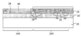
일부 실시예에 있어서, 도 5a에 도시된 바와 같이, 산화는 인접한 트렌치(30) 아래서 성장한 실리콘 게르마늄 산화물 지역(38)이 아직 서로 분리되어 있을 때 종료된다. 따라서 결과적인 NMOS 디바이스(202)(도 11a 및 11b)의 채널 지역의 적어도 일부가 임의의 실리콘 게르마늄 산화물 지역(38)과 중첩되지 않는다. 또한 이들 실시예에 있어서, 실리콘 게르마늄 산화물 지역(38)의 측벽은 수직이 아니며, 또한 곧바르지 않다. 대안적인 실시예에 있어서, 도 5b에 도시된 바와 같이, 산화가 종료되었을 때, 인접한 트렌치(30) 아래서 성장한 실리콘 게르마늄 산화물 지역(38)이 접합된다. 이것은 산화 시간을 연장시킴으로써 달성된다. 이들 실시예에 있어서, 인접한 트렌치들(30) 사이의 반도체층(28)의 부분은 연속적인 실리콘 게르마늄 산화물 지역(38) 위에 위치된다. 반도체층(28)이 NMOS 디바이스[도 11a 및 11b에서 NMOS 디바이스(202)로 지칭하고 있다]를 형성하는데 사용되기 때문에, NMOS 디바이스의 소스/드레인 지역이 기판(20)으로부터 완전히 절연되며, 따라서 누설 전류가 실질적으로 제거된다. In some embodiments, as shown in FIG. 5A, oxidation is terminated when the silicon
도 6에 있어서, 쉘로우 트렌치 아이솔레이션(shallow trench isolation)(STI) 지역(40)이 도 5a 또는 5b에서 트렌치(30)를 충전하도록 형성된다. STI 지역(40)은 실리콘 산화물과 같은 유전체 물질로 트렌치(30)를 충전함으로써 형성되며, 이어서 유전체 물질의 과잉 부분을 제거하기 위해 화학 기계적 폴리시(chemical mechanical polish)(CMP)가 이어진다. 유전체 물질의 나머지 부분은 STI 지역(40)을 형성한다. 또한, 마스크층(32)(도 5a 또는 5b)은 PMOS 디바이스 지역(100)에서 STI 지역(40)의 부분을 형성하기 위해 남아있는 부분을 가질 수도 있다. In FIG. 6, a shallow trench isolation (STI)
도 7은 제2 마스크층(42)의 형성을 도시하고 있다. 일부 실시예에 있어서, 마스크층(42)은 실리콘 질화물과 같은 질화물, 실리콘 산화물과 같은 산화물, 실리콘 옥시질화물과 같은 옥시질화물, 등을 포함한다. 마스크층(42)이 패터닝되므로, 이것은 NMOS 디바이스 지역(200)에는 남아있고, 또한 PMOS 디바이스 지역(100)으로부터는 제거된다. Figure 7 illustrates the formation of a
도 8a 및 8b는 상이한 실시예에 따라 PMOS 디바이스 지역(100)에서 반도체층(28)의 에칭을 도시하고 있으며, 거기에서 마스크층(42)이 에칭 마스크로서 사용된다. 에칭은 습식 에칭 또는 건식 에칭을 사용하여 수행될 수 있다. 습식 에칭이 사용되는 일부 예시적인 실시예에 있어서, 에칭액(etching solution)은 메틸 암모늄 수산화물(methyl ammonium hydroxide)(TMAH), 포타슘 수산화물(potassium hydroxide)(KOH), 등을 포함한다. _____ 와 같은 프로세스 조건은 조정될 수 있으므로, 바닥 표면(44A)은 반도체층(28)의 (551) 표면 평면(들)을 포함한다. 건식 에칭이 사용되는 대안적인 실시예에 있어서, ___ 또는 ___ 이 에칭 가스로서 사용될 수 있다. 8A and 8B illustrate etching of the
에칭 프로세스의 결과로서, 경사진 바닥 표면(44A)이 트렌치(44)의 바닥 표면의 부분으로서 형성된다. 일부 실시예에 있어서, 경사진 바닥 표면(44A)은 반도체층(28)의 실리콘 결정의 (551) 표면 평면상의 (551) 표면이다. 도 8a에 도시된 실시예에 있어서, 트렌치(44)의 전체 바닥 표면은 (551) 표면이며, 이것은 횡단면도에서 V-형상을 형성한다. V-형 바닥 표면은 서로 접합하는 2개의 경사진 (551) 표면 평면을 포함한다. 기판(20)과 반도체 표면층(26, 28)의 주(major) 상부 및 바닥 표면들에 대한 경사각인, 경사진 바닥 표면(44A)의 경사각(α)은 약 8°이다.As a result of the etching process, a sloping
도 8b에 도시된 실시예에 있어서, 경사진 (551) 표면(44A)과 함께, 바닥 표면(44)은 경사진 표면(44A)이 평탄한 표면(44B)의 반대편 단부에 연결된, 평탄한 표면(44B)을 추가로 포함한다. 일부 실시예에 있어서, 기판(20)은 (001) 상부 표면 평면을 가지며, 따라서 평탄한 표면(44B)도 (001) 표면 평면을 갖는다. 바닥 표면들(44A, 44B) 사이에도 형성되는 경사각인, 경사진 바닥 표면(44A)의 경사각(α)은 약 8°이다. 경사각(α)은 반도체 표면층(26, 28)이 기판(20)의 주 상부 및 바닥 표면들에 대해 경사진 바닥 표면(44A)의 각도이기도 한다. 8B, the
에칭 단계에 있어서, 프로세스 조건이 조정될 수 있으므로, (551) 바닥 표면(44A)은 트렌치(44)의 모든 바닥 표면의 중요한 부분이다. 예를 들어, (551) 바닥 표면의 전체 영역은 트렌치(44)의 모든 바닥 표면의 전체 영역의 약 ___ 퍼센트보다 클 수 있다. (551) 바닥 표면(44A)의 영역을 증가시키기 위해, 에칭의 일부 프로세스 조건이 조정된다. 예를 들어, 조정된 프로세스 조건은 ___ 를 포함한다. (551) 평면의 발생 및 확대로 이어질 수 있는 다양한 요소는 에칭액의 화학물(chemical)의 타입, 에칭액의 화학물의 농도, 및 온도, 등을 포함한다. 이들 요소는 조합하여 (551) 바닥 표면(44A)의 영역에 영향을 끼치며, 또한 (551) 바닥 표면(44A)의 큰 영역을 발생시키기 위해 하나의 요소의 변화는 다른 요소의 조정을 필요로 할 수 있다. In the etching step, the
도 8a 및 8b에 도시된 바와 같이, 반도체층(28)의 에칭이 종료되었을 때, 반도체층(28)은 아직 에칭되지 않고 그리고 트렌치(44)의 바닥에 남아있는 바닥층을 갖고 있으며, 그 부분은 예를 들어 5 nm 보다 큰 두께를 갖는다. 따라서 반도체층(26)은 트렌치(44)를 통해서는 노출되지 않는다. 8A and 8B, when the etching of the
다음에, 도 9에 도시된 바와 같이, 에피택시 반도체 지역(46)이 선택적인 에피택시를 통해 트렌치(44)에서 성장하며, 거기에서 반도체 지역(46)은 나머지 반도체층(28)의 상부 표면으로부터 성장하지만, 그러나 노출된 유전체 지역으로부터는 아니다. 일부 실시예에 있어서, 반도체 지역(46)은 Si1-yGey 로 표현되는 실리콘 게르마늄을 포함하며, 여기서 값(Y)은 반도체 지역(46)에서 게르마늄의 원자 백분율이다. 값(Y)은 약 ___(___ 퍼센트) 보다 클 수 있으며, 또한 약 ___ 내지 약 ___ 범위에 있을 수 있다. 값(Y)은 0.1 과 동일할 수도 있으며, 이것은 반도체 지역(46)이 실리콘이 없는 게르마늄층임을 의미한다. 또한, 값(Y)은 반도체층(26)의 값(X)(이것은 Si1-xGex 로 표현된다) 보다 클 수 있으며, 차이(Y-X)는 예를 들어 약 0.1 보다 크고, 약 0.3 보다 크고, 또는 약 0.5 보다 크다. 더 큰 차이(Y-X)는 바람직하게도 반도체 지역(46)에서 더욱 큰 압축률로 나타날 수 있다. 9, an
다음에, 도 10에 도시된 바와 같이, 도 9의 마스크층(42)이 제거된다. 도 10의 구조물의 상부 표면도 예를 들어 CMP 단계에서 평탄화된다. Next, as shown in Fig. 10, the
도 11a 및 11b는 PMOS 디바이스(102) 및 NMOS 디바이스(202)의 형성을 도시하고 있으며, 이것은 채널 지역(103, 203)으로서 반도체 지역(46) 및 반도체층(28)의 부분을 각각 채택하고 있다. PMOS 디바이스(102)와 NMOS 디바이스(202)는 조합하여 CMOS 디바이스로 지칭된다. PMOS 디바이스(102) 및 NMOS 디바이스(202)의 형성은 게이트 유전체(150, 250), 게이트 전극(152, 252), 게이트 스페이서(154, 254), 그리고 소스 및 드레인 지역(156, 256)을 형성하는 단계를 포함한다. 일부 실시예에 있어서, PMOS 디바이스(102) 및 NMOS 디바이스(202)는 평탄한 디바이스이다. 따라서 게이트 유전체(150, 250) 및 게이트 전극(12, 252)이 반도체 지역(46) 및 반도체층(28)의 평탄한 상부 표면 위에 각각 형성된다. Figures 11a and 11b illustrate the formation of a
대안적인 실시예에 있어서, PMOS 디바이스(102) 및 NMOS 디바이스(202)는 핀(fin) 전계효과 트랜지스터(FinFET)이다. 따라서 예를 들어 STI 지역(40)이 60 으로 표시된 레벨(깊이는 커지지는 않는다)로 먼저 리세싱되므로, 에피택시 지역(46) 및 반도체층(28)은 반도체 핀을 형성하도록 STI 지역(40) 위로 돌출한다. 게이트 유전체(150, 250) 및 게이트 전극(152, 252)은 각각의 반도체 핀의 상부 표면 및 측벽 상에 형성되며, 따라서 결과적인 FinFET(102, 202)는 FinFET 이다. In an alternate embodiment,
또한, 도 11a 및 11b는 점선을 도시하고 있으며, 이것은 인접한 트렌치(30) 아래에 형성된 실리콘 게르마늄 산화물 지역(38)이 연속적인 산화물 지역을 형성하도록 접합될 때 실리콘 게르마늄 산화물 지역(38)의 바닥 표면을 도시하고 있으며, 이 실시예는 도 5b에도 도시되어 있다. 11A and 11B also show dotted lines that indicate that the silicon
본 발명의 실시예는 일부 유리한 특징을 갖고 있다. NMOS 디바이스의 소스/드레인 지역(및 가능하기로는 채널)의 아래로 횡방향으로 연장하는 실리콘 게르마늄 산화물 지역을 형성함으로써, 소스/드레인 지역으로부터 기판으로의 누설은 실리콘 게르마늄 산화물 지역의 횡방향 잠식에 의해 방해된다. 실리콘 게르마늄 산화물 지역은 소스/드레인 지역 및 PMOS 디바이스를 위한 채널의 아래로는 연장하지 않으므로, PMOS 디바이스의 압축 응력이 실리콘 게르마늄 산화물 지역에 의해 악영향을 받지는 않는다. PMOS 디바이스가 에피택시 반도체 지역상에 형성되며, 이것은 (551) 표면으로부터 성장된다. 이것은 바람직하게도 에피택시 반도체 지역의 결함의 감소로 나타난다. (551) 표면은 에피택시에 적합하며, 또한 (551) 표면으로부터 성장한 반도체는 더 작은 표면 거칠기를 가지며, 따라서 품질이 향상된다.Embodiments of the invention have some advantageous features. By forming a silicon germanium oxide region extending laterally down the source / drain region (and possibly the channel) of the NMOS device, leakage from the source / drain region to the substrate is caused by lateral encroachment of the silicon germanium oxide region It is disturbed. The silicon germanium oxide region does not extend under the source / drain region and the channel for the PMOS device, so that the compressive stress of the PMOS device is not adversely affected by the silicon germanium oxide region. A PMOS device is formed on the epitaxial semiconductor region, which is grown from the (551) surface. This is preferably due to a reduction in defects in the epitaxial semiconductor region. (551) surface is suitable for epitaxy, and the semiconductor grown from the (551) surface has a smaller surface roughness, thus improving the quality.
일부 실시예에 따라, 디바이스는 제1 반도체층, 및 상기 제1 반도체층 위의 제2 반도체층을 포함한다. 제1 반도체층 및 제2 반도체층은 상이한 물질을 포함한다. 반도체 지역은 제2 반도체층 위에 있고 그리고 이와 접촉하며, 반도체 지역의 바닥 표면은 제2 반도체층의 제1 상부 표면과 접촉한다. 반도체 지역 및 제2 반도체층은 상이한 물질을 포함한다. 반도체 지역의 바닥 표면은 제2 반도체층의 (551) 표면 평면과 접촉하는 경사진 부분을 갖는다. According to some embodiments, the device includes a first semiconductor layer, and a second semiconductor layer over the first semiconductor layer. The first semiconductor layer and the second semiconductor layer comprise different materials. The semiconductor region is over and in contact with the second semiconductor layer, and the bottom surface of the semiconductor region is in contact with the first upper surface of the second semiconductor layer. The semiconductor region and the second semiconductor layer comprise different materials. The bottom surface of the semiconductor region has a sloped portion in contact with the surface planar surface of the second semiconductor layer (551).
다른 실시예에 따라, 디바이스는 실리콘 기판, 제1 게르마늄 백분율을 갖는 실리콘 게르마늄층, 상기 실리콘 게르마늄층 위의 실리콘층, 및 제1 상부 표면 위의 그리고 이와 접촉하는 바닥 표면을 갖는 실리콘 게르마늄 지역을 포함한다. 실리콘 게르마늄 지역은 제1 실리콘 게르마늄 백분율보다 큰 제2 게르마늄 백분율을 갖는다. PMOS 디바이스는 실리콘 게르마늄 지역 위에 제1 게이트 유전체를 포함한다. NMOS 디바이스는 실리콘층의 제2 상부 표면 위에 제2 게이트 유전체, 및 상기 제2 유전체 게이트에 인접한 소스/드레인 지역을 포함한다. STI 지역은 실리콘층에 있으며, 거기에서 제1 STI 지역이 소스/드레인 지역과 접촉한다. 실리콘 게르마늄 산화물 지역은 실리콘 게르마늄층에 있다. 실리콘 게르마늄 산화물 지역은 제1 STI 지역의 아래에서 그리고 이와 접촉하는 제1 부분, 및 NMOS 디바이스의 소스/드레인 지역에 의해 중첩되는 제2 부분을 포함한다. According to another embodiment, the device includes a silicon germanium region having a silicon substrate, a silicon germanium layer having a first germanium percentage, a silicon layer over the silicon germanium layer, and a bottom surface over and in contact with the first upper surface do. The silicon germanium region has a second germanium percentage greater than the first silicon germanium percentage. The PMOS device includes a first gate dielectric over the silicon germanium region. The NMOS device includes a second gate dielectric over the second upper surface of the silicon layer, and a source / drain region adjacent the second dielectric gate. The STI region is in the silicon layer where the first STI region contacts the source / drain region. The silicon germanium oxide region is in the silicon germanium layer. The silicon germanium oxide region includes a first portion under and in contact with the first STI region, and a second portion overlapping by the source / drain region of the NMOS device.
또 다른 실시예에 따라, 방법은 기판 위에 실리콘 게르마늄층을 형성하기 위해 제1 에피택시를 수행하는 단계, 및 실리콘 게르마늄층 위에 실리콘층을 형성하기 위해 제2 에피택시를 수행하는 단계를 포함하며, 상기 실리콘 게르마늄층은 제1 게르마늄 백분율을 갖는다. 실리콘층은 트렌치를 형성하도록 에칭되며, 실리콘층의 바닥 부분은 트렌치 아래에 남아있다. 실리콘층의 바닥 부분은 경사진 부분을 포함하는 상부 표면을 가지며, 상기 경사진 부분은 실리콘층의 (551) 평면을 포함한다. 트렌치에 실리콘 게르마늄 지역을 형성하기 위해, 제3 에피택시가 수행된다. 실리콘 게르마늄 지역은 실리콘층의 상부 표면 위의 그리고 이와 접촉하는 바닥 표면을 갖는다. 상기 방법은 PMOS 디바이스를 형성하는 단계를 더 포함하며, 그 형성은 실리콘 게르마늄 지역에 PMOS 디바이스의 채널 지역을 구비한, 실리콘 게르마늄 지역의 상부 표면 위에 게이트 유전체를 형성하는 단계를 포함한다.According to yet another embodiment, a method includes performing a first epitaxy to form a silicon germanium layer on a substrate, and performing a second epitaxy to form a silicon layer over the silicon germanium layer, The silicon germanium layer has a first germanium percentage. The silicon layer is etched to form trenches, and the bottom portion of the silicon layer remains under the trenches. The bottom portion of the silicon layer has a top surface that includes a sloped portion, and the sloped portion includes a (551) plane of the silicon layer. To form the silicon germanium region in the trench, a third epitaxy is performed. The silicon germanium region has a bottom surface on and in contact with the top surface of the silicon layer. The method further comprises forming a PMOS device, the formation of which comprises forming a gate dielectric over the upper surface of the silicon germanium region, with the channel region of the PMOS device in the silicon germanium region.
실시예 및 그 장점이 상세히 설명되었지만, 첨부된 청구범위에 의해 한정된 바와 같이 실시예의 정신 및 범위로부터의 일탈 없이 여기에 다양한 변화, 치환, 및 변경이 이루어질 수 있음을 인식해야 한다. 더욱이, 이 출원의 범위는 명세서에 설명된 프로세스, 장치, 제조, 및 물질의 조성물, 수단, 방법, 및 단계를 제한하는 것으로 의도되지 않는다. 당업자 중 하나라면 기재된 바로부터 여기에 설명된 대응하는 실시예와 실질적으로 동일한 기능을 수행하거나 또는 실질적으로 동일한 결과를 달성하는 현재 존재하는 또는 나중에 개발될 프로세스, 장치, 제조, 물질의 조성물, 수단, 방법, 또는 단계가 설명에 따라 사용될 수 있음을 용이하게 인식할 것이다. 따라서 첨부된 청구범위는 프로세스, 장치, 제조, 물질의 조성물, 수단, 방법, 또는 단계와 같은 그 범위 내에 포함되는 것으로 의도된다. 또한, 각각의 청구범위는 별도의 실시예를 구성하며, 또한 다양한 청구범위와 실시예의 조합이 이 설명의 범위 내에 있다. Although the embodiments and advantages thereof have been described in detail, it should be understood that various changes, substitutions and alterations can be made herein without departing from the spirit and scope of the embodiments as defined by the appended claims. Moreover, the scope of this application is not intended to limit the process, apparatus, manufacture, and compositions, means, methods, and steps of the materials set forth in the specification. One of ordinary skill in the art will appreciate that the present invention may be practiced otherwise than as described herein without departing from the spirit and scope of the present invention, Method, or step may be used in accordance with the description. Accordingly, the appended claims are intended to be encompassed within the scope of such processes, devices, manufacture, compositions of matter, means, methods, or steps. Furthermore, each claim constitutes a separate embodiment, and a combination of various claims and embodiments is also within the scope of this description.
Claims (20)
제1 반도체층;
상기 제1 반도체층 위의 제2 반도체층;
상기 제2 반도체층 위의 그리고 이와 접촉하는 반도체 지역
을 포함하며,
상기 제1 반도체층 및 제2 반도체층은 상이한 물질을 포함하며, 상기 반도체 지역의 바닥 표면은 상기 제2 반도체층의 제1 상부 표면과 접촉하며, 상기 반도체 지역 및 상기 제2 반도체층은 상이한 물질을 포함하며, 상기 반도체 지역의 바닥 표면은 제2 반도체층의 제1 (551) 표면 평면과 접촉하는 경사진 제1 부분을 포함하는, 디바이스.As a device,
A first semiconductor layer;
A second semiconductor layer over the first semiconductor layer;
A semiconductor region over and in contact with the second semiconductor layer
/ RTI >
Wherein the first semiconductor layer and the second semiconductor layer comprise a different material and the bottom surface of the semiconductor region is in contact with a first upper surface of the second semiconductor layer and wherein the semiconductor region and the second semiconductor layer are different materials Wherein the bottom surface of the semiconductor region comprises a sloped first portion in contact with a first (551) surface plane of the second semiconductor layer.
상기 제2 반도체층의 제2 상부 표면으로부터 상기 제2 반도체층 내로 연장하며, 상기 제2 반도체층의 제2 상부 표면이 상기 제2 반도체층의 제1 상부 표면보다 높은 쉘로우 트렌치 아이솔레이션(Shallow Trench Isolation; STI) 지역;
N-타입 금속-산화물-반도체(NMOS) 디바이스; 및
상기 제1 반도체층의 산화물 지역
을 더 포함하며,
상기 N-타입 금속-산화물-반도체(NMOS) 디바이스는,
제2 채널 지역으로서 상기 제2 반도체층의 일부;
상기 제2 채널 지역 위의 게이트 스택; 및
상기 제2 채널 지역과 상기 STI 지역 사이의 소스/드레인 지역
을 포함하며,
상기 소스/드레인 지역은 상기 STI 지역의 엣지와 접촉하며,
상기 산화물 지역은 STI 지역의 엣지를 지나 연장하고, 또한 상기 소스/드레인 지역에 의해 중첩되는 부분을 포함하는, 디바이스.2. The device of claim 1, further comprising: a P-type metal-oxide-semiconductor (PMOS) device including a portion of the semiconductor region as a first channel region;
A second upper surface of the second semiconductor layer extending from the second upper surface of the second semiconductor layer into the second semiconductor layer and having a shallow trench isolation ; STI) region;
N-type metal-oxide-semiconductor (NMOS) devices; And
The oxide region of the first semiconductor layer
Further comprising:
The N-type metal-oxide-semiconductor (NMOS)
A portion of the second semiconductor layer as a second channel region;
A gate stack over the second channel region; And
Drain region between the second channel region and the STI region
/ RTI >
The source / drain region is in contact with an edge of the STI region,
Wherein the oxide region extends beyond an edge of the STI region and also includes a portion overlapped by the source / drain region.
실리콘 기판;
제1 게르마늄 백분율을 갖는 실리콘 게르마늄층;
상기 실리콘 게르마늄층 위의 실리콘층;
상기 실리콘층의 제1 상부 표면 위의 그리고 이와 접촉하는 바닥 표면을 가지며, 상기 제1 게르마늄 백분율보다 높은 제2 게르마늄 백분율을 갖는 실리콘 게르마늄 지역;
P-타입 금속-산화물-반도체(PMOS) 디바이스;
N-타입 금속-산화물-반도체(NMOS) 디바이스;
소스/드레인 지역과 접촉하는, 상기 실리콘층의 제1 쉘로우 트렌치 아이솔레이션(STI) 지역; 및
상기 실리콘 게르마늄층의 제1 실리콘 게르마늄 산화물 지역
을 포함하며,
상기 P-타입 금속-산화물-반도체(PMOS) 디바이스는,
상기 실리콘 게르마늄 지역 위의 제1 게이트 유전체를 포함하며,
상기 N-타입 금속-산화물-반도체(NMOS) 디바이스는,
상기 실리콘층의 제2 상부 표면 위의 제2 게이트 유전체; 및
상기 제2 게이트 유전체에 인접한 소스/드레인 지역
을 포함하며,
상기 제1 실리콘 게르마늄 산화물 지역은,
상기 제1 STI 지역의 아래에서 그리고 이와 접촉하는 제1 부분; 및
상기 NMOS 디바이스의 소스/드레인 지역에 의해 중첩되는 제2 부분
을 포함하는, 디바이스.As a device,
A silicon substrate;
A silicon germanium layer having a first germanium percentage;
A silicon layer on the silicon germanium layer;
A silicon germanium region having a second germanium percentage higher than the first germanium percentage, the silicon germanium region having a bottom surface on and in contact with the first upper surface of the silicon layer;
P-type metal-oxide-semiconductor (PMOS) devices;
N-type metal-oxide-semiconductor (NMOS) devices;
A first shallow trench isolation (STI) region of the silicon layer in contact with a source / drain region; And
The first silicon germanium oxide region of the silicon germanium layer
/ RTI >
The P-type metal-oxide-semiconductor (PMOS)
A first gate dielectric over the silicon germanium region,
The N-type metal-oxide-semiconductor (NMOS)
A second gate dielectric over the second upper surface of the silicon layer; And
A source / drain region adjacent said second gate dielectric
/ RTI >
Wherein the first silicon germanium oxide region is a silicon germanium oxide region,
A first portion below and in contact with the first STI region; And
A second portion overlapping by the source / drain region of the NMOS device;
/ RTI >
상기 추가적인 소스/드레인 지역과 접촉하는, 상기 실리콘층의 제2 STI 지역; 및
상기 실리콘 게르마늄층의 제2 실리콘 게르마늄 산화물 지역
을 더 포함하며,
상기 추가적인 소스/드레인 지역은 제1 게이트 유전체에 인접하며, 상기 실리콘 게르마늄 지역의 일부는 상기 추가적인 소스/드레인 지역의 일부를 형성하며,
상기 제2 실리콘 게르마늄 산화물 지역의 전체는 상기 추가적인 소스/드레인 지역에 의해 중첩되지 않는, 디바이스. 10. The device of claim 9, further comprising: an additional source / drain region included in the PMOS device;
A second STI region of the silicon layer in contact with the additional source / drain region; And
The second silicon germanium oxide region of the silicon germanium layer
Further comprising:
The additional source / drain region is adjacent a first gate dielectric, and wherein a portion of the silicon germanium region forms part of the additional source / drain region,
Wherein the entirety of the second silicon germanium oxide region is not overlapped by the additional source / drain region.
상기 실리콘 게르마늄층 위에 실리콘층을 형성하기 위해 제2 에피택시를 수행하는 것;
트렌치를 형성하도록 실리콘층을 에칭하는 것;
상기 트렌치에 실리콘 게르마늄 지역을 형성하기 위해 제3 에피택시를 수행하는 것; 및
P-타입 금속-산화물-반도체(PMOS) 디바이스를 형성하는 것
을 포함하며,
상기 실리콘 게르마늄층은 제1 게르마늄 백분율을 가지며,
상기 실리콘층의 바닥 부분은 상기 트렌치 아래에 남겨지며, 상기 실리콘층의 바닥 부분은 경사진 제1 부분을 포함하는 상부 표면을 가지며, 상기 경사진 제1 부분은 상기 실리콘층의 (551) 평면을 포함하며,
상기 실리콘 게르마늄 지역은 상기 실리콘층의 상부 표면 위의 그리고 이와 접촉하는 바닥 표면을 가지며,
상기 P-타입 금속-산화물-반도체(PMOS) 디바이스를 형성하는 것은,
상기 실리콘 게르마늄 지역에 상기 PMOS 디바이스의 채널 지역을 구비한, 상기 실리콘 게르마늄 지역의 상부 표면 위에 제1 게이트 유전체를 형성하는 것을 포함하는, 방법.Performing a first epitaxy to form a silicon germanium layer on the substrate;
Performing a second epitaxy to form a silicon layer on the silicon germanium layer;
Etching the silicon layer to form a trench;
Performing a third epitaxy to form a silicon germanium region in the trench; And
Forming a P-type metal-oxide-semiconductor (PMOS) device
/ RTI >
Wherein the silicon germanium layer has a first germanium percentage,
Wherein a bottom portion of the silicon layer is left under the trench and a bottom portion of the silicon layer has an upper surface comprising a sloped first portion and the sloped first portion has a (551) plane of the silicon layer ≪ / RTI &
The silicon germanium region having a bottom surface on and in contact with the top surface of the silicon layer,
The formation of the P-type metal-oxide-semiconductor (PMOS)
And forming a first gate dielectric over the upper surface of the silicon germanium region, wherein the first germanium region has a channel region of the PMOS device in the silicon germanium region.
상기 추가적인 제1 트렌치의 바닥 및 측벽을 덮기 위해 마스크층을 형성하는 것;
상기 실리콘 게르마늄층에 실리콘 게르마늄 산화물 지역을 형성하기 위해, 상기 추가적인 제2 트렌치를 통해 상기 실리콘 게르마늄층상에 산화를 수행하는 것;
제1 쉘로우 트렌치 아이솔레이션(STI) 지역 및 제2 STI 지역을 각각 형성하기 위해, 상기 추가적인 제1 트렌치 및 상기 추가적인 제2 트렌치를 충전하는 것; 및
N-타입 금속-산화물-반도체(NMOS) 디바이스를 형성하는 것
을 더 포함하며,
상기 추가적인 제2 트렌치의 측벽 및 바닥은 마스크층에 의해 덮이지 않으며,
상기 N-타입 금속-산화물-반도체(NMOS) 디바이스를 형성하는 것은,
상기 실리콘층의 일부가 상기 NMOS 디바이스의 채널 지역인, 상기 실리콘층 위에 제2 게이트 유전체를 형성하는 것; 및
상기 제2 게이트 유전체에 인접하여 소스/드레인 지역을 형성하는 것
을 포함하며,
상기 소스/드레인 지역의 일부는 상기 실리콘 게르마늄 산화물 지역의 일부와 중첩되는, 방법.16. The method of claim 15, further comprising: forming an additional first trench and an additional second trench in the silicon layer prior to etching the silicon layer to form the trench; And
Forming a mask layer to cover the bottom and side walls of the additional first trench;
Performing oxidation on the silicon germanium layer through the additional second trench to form a silicon germanium oxide region in the silicon germanium layer;
Filling the additional first trench and the additional second trench to form a first shallow trench isolation (STI) region and a second STI region, respectively; And
Forming an N-type metal-oxide-semiconductor (NMOS) device
Further comprising:
The sidewalls and bottom of the additional second trench are not covered by the mask layer,
The formation of the N-type metal-oxide-semiconductor (NMOS)
Forming a second gate dielectric over the silicon layer, wherein a portion of the silicon layer is a channel region of the NMOS device; And
Forming a source / drain region adjacent the second gate dielectric
/ RTI >
Wherein a portion of the source / drain region overlaps with a portion of the silicon germanium oxide region.
Applications Claiming Priority (2)
| Application Number | Priority Date | Filing Date | Title |
|---|---|---|---|
| US14/087,425 US9224734B2 (en) | 2013-09-13 | 2013-11-22 | CMOS devices with reduced leakage and methods of forming the same |
| US14/087,425 | 2013-11-22 |
Publications (2)
| Publication Number | Publication Date |
|---|---|
| KR20150059633A true KR20150059633A (en) | 2015-06-01 |
| KR101622048B1 KR101622048B1 (en) | 2016-05-17 |
Family
ID=53181898
Family Applications (1)
| Application Number | Title | Priority Date | Filing Date |
|---|---|---|---|
| KR1020140164541A Active KR101622048B1 (en) | 2013-11-22 | 2014-11-24 | Cmos devices with reduced leakage and methods of forming the same |
Country Status (3)
| Country | Link |
|---|---|
| US (2) | US9224734B2 (en) |
| KR (1) | KR101622048B1 (en) |
| CN (1) | CN104659046B (en) |
Families Citing this family (24)
| Publication number | Priority date | Publication date | Assignee | Title |
|---|---|---|---|---|
| US9818761B2 (en) * | 2015-06-25 | 2017-11-14 | International Business Machines Corporation | Selective oxidation for making relaxed silicon germanium on insulator structures |
| US9443873B1 (en) * | 2015-12-14 | 2016-09-13 | International Business Machines Corporation | Structure and method for tensile and compressive strained silicon germanium with same germanium concentration by single epitaxy step |
| US10020186B2 (en) * | 2016-07-29 | 2018-07-10 | Applied Materials, Inc. | Silicon germanium selective oxidation process |
| KR102707542B1 (en) | 2016-12-02 | 2024-09-20 | 삼성전자주식회사 | Semiconductor memory device and method of forming the same |
| US10224224B2 (en) | 2017-03-10 | 2019-03-05 | Micromaterials, LLC | High pressure wafer processing systems and related methods |
| US10622214B2 (en) | 2017-05-25 | 2020-04-14 | Applied Materials, Inc. | Tungsten defluorination by high pressure treatment |
| US10134901B1 (en) | 2017-06-26 | 2018-11-20 | Globalfoundries Inc. | Methods of forming a bulk field effect transistor (FET) with sub-source/drain isolation layers and the resulting structures |
| JP6947914B2 (en) | 2017-08-18 | 2021-10-13 | アプライド マテリアルズ インコーポレイテッドApplied Materials,Incorporated | Annealing chamber under high pressure and high temperature |
| US10276411B2 (en) | 2017-08-18 | 2019-04-30 | Applied Materials, Inc. | High pressure and high temperature anneal chamber |
| CN107527926B (en) * | 2017-08-25 | 2020-02-07 | 惠科股份有限公司 | Active array switch substrate and display panel thereof |
| EP4321649B1 (en) | 2017-11-11 | 2025-08-20 | Micromaterials LLC | Gas delivery system for high pressure processing chamber |
| JP2021503714A (en) | 2017-11-17 | 2021-02-12 | アプライド マテリアルズ インコーポレイテッドApplied Materials,Incorporated | Capacitor system for high pressure processing system |
| SG11202008256WA (en) | 2018-03-09 | 2020-09-29 | Applied Materials Inc | High pressure annealing process for metal containing materials |
| US10950429B2 (en) | 2018-05-08 | 2021-03-16 | Applied Materials, Inc. | Methods of forming amorphous carbon hard mask layers and hard mask layers formed therefrom |
| US10790183B2 (en) | 2018-06-05 | 2020-09-29 | Applied Materials, Inc. | Selective oxidation for 3D device isolation |
| US10748783B2 (en) | 2018-07-25 | 2020-08-18 | Applied Materials, Inc. | Gas delivery module |
| CN110828566B (en) * | 2018-08-13 | 2023-03-31 | 世界先进积体电路股份有限公司 | Semiconductor structure and forming method thereof |
| CN110858561A (en) * | 2018-08-23 | 2020-03-03 | 合肥晶合集成电路有限公司 | Silicon island structure and method of making the same |
| US10600919B1 (en) * | 2018-10-03 | 2020-03-24 | Vanguard International Semiconductor Corporation | Semiconductor structure and method for forming the same |
| WO2020117462A1 (en) | 2018-12-07 | 2020-06-11 | Applied Materials, Inc. | Semiconductor processing system |
| US11901222B2 (en) | 2020-02-17 | 2024-02-13 | Applied Materials, Inc. | Multi-step process for flowable gap-fill film |
| US11075078B1 (en) * | 2020-03-06 | 2021-07-27 | Atomera Incorporated | Method for making a semiconductor device including a superlattice within a recessed etch |
| US11869802B2 (en) * | 2020-07-29 | 2024-01-09 | Changxin Memory Technologies, Inc. | Method of forming semiconductor isolation structure and semiconductor isolation structure |
| CN114068389B (en) * | 2020-07-29 | 2024-08-02 | 长鑫存储技术有限公司 | Method for forming semiconductor structure and semiconductor structure |
Family Cites Families (20)
| Publication number | Priority date | Publication date | Assignee | Title |
|---|---|---|---|---|
| KR100437856B1 (en) | 2002-08-05 | 2004-06-30 | 삼성전자주식회사 | MOS Transister and Method of manufacturing semiconductor device comprising the same |
| KR20040014716A (en) | 2002-08-10 | 2004-02-18 | 한국전자통신연구원 | Method of manufacturing semiconductor device having oxide layer under active region |
| US7662689B2 (en) | 2003-12-23 | 2010-02-16 | Intel Corporation | Strained transistor integration for CMOS |
| JP4369359B2 (en) * | 2004-12-28 | 2009-11-18 | 富士通マイクロエレクトロニクス株式会社 | Semiconductor device |
| KR100717503B1 (en) | 2005-08-11 | 2007-05-14 | 동부일렉트로닉스 주식회사 | Semiconductor device and manufacturing method thereof |
| CN101322240B (en) * | 2005-12-02 | 2011-12-14 | 国立大学法人东北大学 | Semiconductor device |
| KR101070204B1 (en) * | 2006-02-01 | 2011-10-06 | 자이단호진 고쿠사이카가쿠 신고우자이단 | Semiconductor device manufacturing method and method for reducing microroughness of semiconductor surface |
| US8853746B2 (en) | 2006-06-29 | 2014-10-07 | International Business Machines Corporation | CMOS devices with stressed channel regions, and methods for fabricating the same |
| EP2442357A3 (en) * | 2006-07-13 | 2012-07-11 | National University Corporation Tohoku Unversity | Semiconductor device |
| US8558278B2 (en) * | 2007-01-16 | 2013-10-15 | Taiwan Semiconductor Manufacturing Company, Ltd. | Strained transistor with optimized drive current and method of forming |
| DE102007004862B4 (en) * | 2007-01-31 | 2014-01-30 | Globalfoundries Inc. | A method of fabricating Si-Ge containing drain / source regions in lower Si / Ge loss transistors |
| US7700452B2 (en) * | 2007-08-29 | 2010-04-20 | Taiwan Semiconductor Manufacturing Company, Ltd. | Strained channel transistor |
| US20100109044A1 (en) * | 2008-10-30 | 2010-05-06 | Tekleab Daniel G | Optimized Compressive SiGe Channel PMOS Transistor with Engineered Ge Profile and Optimized Silicon Cap Layer |
| JP2010219152A (en) * | 2009-03-13 | 2010-09-30 | Toshiba Corp | Semiconductor apparatus and method of manufacturing the same |
| US8378476B2 (en) | 2010-03-25 | 2013-02-19 | Stats Chippac Ltd. | Integrated circuit packaging system with stacking option and method of manufacture thereof |
| US8395213B2 (en) * | 2010-08-27 | 2013-03-12 | Acorn Technologies, Inc. | Strained semiconductor using elastic edge relaxation of a stressor combined with buried insulating layer |
| US9006786B2 (en) * | 2013-07-03 | 2015-04-14 | Taiwan Semiconductor Manufacturing Company, Ltd. | Fin structure of semiconductor device |
| US9735255B2 (en) * | 2013-01-18 | 2017-08-15 | Taiwan Semiconductor Manufacturing Company, Ltd. | Method for fabricating a finFET device including a stem region of a fin element |
| US9006842B2 (en) * | 2013-05-30 | 2015-04-14 | Taiwan Semiconductor Manufacturing Company, Ltd. | Tuning strain in semiconductor devices |
| US9553012B2 (en) * | 2013-09-13 | 2017-01-24 | Taiwan Semiconductor Manufacturing Company Ltd. | Semiconductor structure and the manufacturing method thereof |
-
2013
- 2013-11-22 US US14/087,425 patent/US9224734B2/en not_active Expired - Fee Related
-
2014
- 2014-11-24 CN CN201410683088.1A patent/CN104659046B/en not_active Expired - Fee Related
- 2014-11-24 KR KR1020140164541A patent/KR101622048B1/en active Active
-
2015
- 2015-12-04 US US14/959,355 patent/US9390982B2/en active Active
Also Published As
| Publication number | Publication date |
|---|---|
| US20160086862A1 (en) | 2016-03-24 |
| US20150145002A1 (en) | 2015-05-28 |
| CN104659046B (en) | 2017-12-19 |
| US9390982B2 (en) | 2016-07-12 |
| KR101622048B1 (en) | 2016-05-17 |
| CN104659046A (en) | 2015-05-27 |
| US9224734B2 (en) | 2015-12-29 |
Similar Documents
| Publication | Publication Date | Title |
|---|---|---|
| KR101622048B1 (en) | Cmos devices with reduced leakage and methods of forming the same | |
| KR101857917B1 (en) | Semiconductor structure and manufacturing method thereof | |
| US9805942B2 (en) | Method of modifying epitaxial growth shape on source drain area of transistor | |
| US10014224B2 (en) | Structure and formation method of fin-like field effect transistor | |
| US8633516B1 (en) | Source/drain stack stressor for semiconductor device | |
| US9099388B2 (en) | III-V multi-channel FinFETs | |
| US10037921B2 (en) | Structure and formation method of fin-like field effect transistor | |
| CN103094089B (en) | Fin formula field effect transistor gate oxide | |
| US9276117B1 (en) | Structure and method and FinFET device | |
| US20110193167A1 (en) | Self-Aligned Two-Step STI Formation Through Dummy Poly Removal | |
| US8716076B2 (en) | Method for fabricating a semiconductor device having an epitaxial channel and transistor having same | |
| US9385234B2 (en) | FinFETs with strained well regions | |
| JP6786755B2 (en) | Methods and Related Semiconductor Structures for Fabricating Semiconductor Structures Containing Fin Structures with Different Strained States | |
| CN105575778A (en) | Semiconductor device and manufacturing method thereof | |
| US9859425B2 (en) | Field-effect transistor with aggressively strained fins | |
| US10818560B2 (en) | Vertical field-effect transistor (VFET) devices and methods of forming the same | |
| EP1638149A2 (en) | Method of manufacture of an heterostructure channel insulated gate field effect transistor and corresponding transistor | |
| US9093473B2 (en) | Method for fabricating metal-oxide semiconductor transistor | |
| JP2011199112A (en) | Semiconductor device, and method of manufacturing the same | |
| US9847393B2 (en) | Semiconductor device | |
| KR102422158B1 (en) | Semiconductor device and method for manufacturing the same |
Legal Events
| Date | Code | Title | Description |
|---|---|---|---|
| PA0109 | Patent application |
Patent event code: PA01091R01D Comment text: Patent Application Patent event date: 20141124 |
|
| A201 | Request for examination | ||
| PA0201 | Request for examination |
Patent event code: PA02012R01D Patent event date: 20150102 Comment text: Request for Examination of Application Patent event code: PA02011R01I Patent event date: 20141124 Comment text: Patent Application |
|
| PG1501 | Laying open of application | ||
| E902 | Notification of reason for refusal | ||
| PE0902 | Notice of grounds for rejection |
Comment text: Notification of reason for refusal Patent event date: 20151111 Patent event code: PE09021S01D |
|
| E701 | Decision to grant or registration of patent right | ||
| PE0701 | Decision of registration |
Patent event code: PE07011S01D Comment text: Decision to Grant Registration Patent event date: 20160218 |
|
| GRNT | Written decision to grant | ||
| PR0701 | Registration of establishment |
Comment text: Registration of Establishment Patent event date: 20160511 Patent event code: PR07011E01D |
|
| PR1002 | Payment of registration fee |
Payment date: 20160511 End annual number: 3 Start annual number: 1 |
|
| PG1601 | Publication of registration | ||
| FPAY | Annual fee payment |
Payment date: 20190425 Year of fee payment: 4 |
|
| PR1001 | Payment of annual fee |
Payment date: 20190425 Start annual number: 4 End annual number: 4 |
|
| PR1001 | Payment of annual fee |
Payment date: 20210430 Start annual number: 6 End annual number: 6 |
|
| PR1001 | Payment of annual fee |
Payment date: 20220428 Start annual number: 7 End annual number: 7 |
|
| PR1001 | Payment of annual fee |
Payment date: 20230426 Start annual number: 8 End annual number: 8 |
|
| PR1001 | Payment of annual fee |
Payment date: 20240425 Start annual number: 9 End annual number: 9 |