KR101443390B1 - Data modulation method, liquid crystal display device having the same, and driving method thereof - Google Patents
Data modulation method, liquid crystal display device having the same, and driving method thereof Download PDFInfo
- Publication number
- KR101443390B1 KR101443390B1 KR1020080038907A KR20080038907A KR101443390B1 KR 101443390 B1 KR101443390 B1 KR 101443390B1 KR 1020080038907 A KR1020080038907 A KR 1020080038907A KR 20080038907 A KR20080038907 A KR 20080038907A KR 101443390 B1 KR101443390 B1 KR 101443390B1
- Authority
- KR
- South Korea
- Prior art keywords
- data
- negative
- positive
- frame
- voltage
- Prior art date
- Legal status (The legal status is an assumption and is not a legal conclusion. Google has not performed a legal analysis and makes no representation as to the accuracy of the status listed.)
- Expired - Fee Related
Links
Images


Classifications
-
- G—PHYSICS
- G09—EDUCATION; CRYPTOGRAPHY; DISPLAY; ADVERTISING; SEALS
- G09G—ARRANGEMENTS OR CIRCUITS FOR CONTROL OF INDICATING DEVICES USING STATIC MEANS TO PRESENT VARIABLE INFORMATION
- G09G3/00—Control arrangements or circuits, of interest only in connection with visual indicators other than cathode-ray tubes
- G09G3/20—Control arrangements or circuits, of interest only in connection with visual indicators other than cathode-ray tubes for presentation of an assembly of a number of characters, e.g. a page, by composing the assembly by combination of individual elements arranged in a matrix no fixed position being assigned to or needed to be assigned to the individual characters or partial characters
- G09G3/2007—Display of intermediate tones
- G09G3/2044—Display of intermediate tones using dithering
- G09G3/2051—Display of intermediate tones using dithering with use of a spatial dither pattern
-
- G—PHYSICS
- G09—EDUCATION; CRYPTOGRAPHY; DISPLAY; ADVERTISING; SEALS
- G09G—ARRANGEMENTS OR CIRCUITS FOR CONTROL OF INDICATING DEVICES USING STATIC MEANS TO PRESENT VARIABLE INFORMATION
- G09G3/00—Control arrangements or circuits, of interest only in connection with visual indicators other than cathode-ray tubes
- G09G3/20—Control arrangements or circuits, of interest only in connection with visual indicators other than cathode-ray tubes for presentation of an assembly of a number of characters, e.g. a page, by composing the assembly by combination of individual elements arranged in a matrix no fixed position being assigned to or needed to be assigned to the individual characters or partial characters
- G09G3/2007—Display of intermediate tones
- G09G3/2011—Display of intermediate tones by amplitude modulation
-
- G—PHYSICS
- G09—EDUCATION; CRYPTOGRAPHY; DISPLAY; ADVERTISING; SEALS
- G09G—ARRANGEMENTS OR CIRCUITS FOR CONTROL OF INDICATING DEVICES USING STATIC MEANS TO PRESENT VARIABLE INFORMATION
- G09G3/00—Control arrangements or circuits, of interest only in connection with visual indicators other than cathode-ray tubes
- G09G3/20—Control arrangements or circuits, of interest only in connection with visual indicators other than cathode-ray tubes for presentation of an assembly of a number of characters, e.g. a page, by composing the assembly by combination of individual elements arranged in a matrix no fixed position being assigned to or needed to be assigned to the individual characters or partial characters
- G09G3/34—Control arrangements or circuits, of interest only in connection with visual indicators other than cathode-ray tubes for presentation of an assembly of a number of characters, e.g. a page, by composing the assembly by combination of individual elements arranged in a matrix no fixed position being assigned to or needed to be assigned to the individual characters or partial characters by control of light from an independent source
- G09G3/36—Control arrangements or circuits, of interest only in connection with visual indicators other than cathode-ray tubes for presentation of an assembly of a number of characters, e.g. a page, by composing the assembly by combination of individual elements arranged in a matrix no fixed position being assigned to or needed to be assigned to the individual characters or partial characters by control of light from an independent source using liquid crystals
- G09G3/3611—Control of matrices with row and column drivers
- G09G3/3614—Control of polarity reversal in general
-
- G—PHYSICS
- G09—EDUCATION; CRYPTOGRAPHY; DISPLAY; ADVERTISING; SEALS
- G09G—ARRANGEMENTS OR CIRCUITS FOR CONTROL OF INDICATING DEVICES USING STATIC MEANS TO PRESENT VARIABLE INFORMATION
- G09G2300/00—Aspects of the constitution of display devices
- G09G2300/08—Active matrix structure, i.e. with use of active elements, inclusive of non-linear two terminal elements, in the pixels together with light emitting or modulating elements
- G09G2300/0809—Several active elements per pixel in active matrix panels
- G09G2300/0823—Several active elements per pixel in active matrix panels used to establish symmetry in driving, e.g. with polarity inversion
Landscapes
- Engineering & Computer Science (AREA)
- Physics & Mathematics (AREA)
- Computer Hardware Design (AREA)
- General Physics & Mathematics (AREA)
- Theoretical Computer Science (AREA)
- Chemical & Material Sciences (AREA)
- Crystallography & Structural Chemistry (AREA)
- Control Of Indicators Other Than Cathode Ray Tubes (AREA)
Abstract
데이터 변조 방법, 이를 구비한 액정표시장치 및 그 구동 방법이 개시된다.A data modulation method, a liquid crystal display device having the same, and a driving method thereof are disclosed.
본 발명의 데이터 변조 방법은, n비트의 데이터 신호로부터 상위 m비트를 갖는 제1 데이터와 하위 (n-m)비트 데이터를 분리하는 단계; 및 상기 제1 데이터와 상기 제1 데이터보다 1계조 높은 제2 데이터를 바탕으로 프레임별로 정극성 데이터와 부극성 데이터를 생성하는 단계를 포함한다.A data modulation method of the present invention includes: separating first data having an upper m bits and lower (n-m) bit data from an n bit data signal; And generating positive polarity data and negative polarity data for each frame on the basis of the first data and the second data one level higher than the first data.
따라서, 본 발명은 정극성 감마 전압과 부극성 감마 전압 사이의 차이를 이용하여 프레임 레이트 변조함으로써, 프레임 수가 종래에 비해 적어도 절반 이하로 줄어들어 프레임 노이즈를 현저히 줄일 수 있다. Therefore, the present invention can reduce the frame noise by reducing the frame number to at least half or less by using the difference between the positive gamma voltage and the negative gamma voltage.
액정표시장치, 프레임 레이트 제어, FRC, 공통전압, 노이즈 Liquid crystal display, Frame rate control, FRC, Common voltage, Noise
Description
본 발명은 데이터 변조에 관한 것으로서, 특히 비트 확장을 위한 데이터 변조 방법, 이를 구비한 액정표시장치 및 그 구동 방법에 관한 것이다.BACKGROUND OF THE
정보화 사회의 발달로 인해, 정보를 표시할 수 있는 표시 장치가 활발히 개발되고 있다. 표시 장치는 액정표시장치(liquid crystal display device), 유기전계발광 표시장치(organic electro-luminescence display device), 플라즈마 표시장치(plasma display panel) 및 전계 방출 표시장치(field emission display device)를 포함한다.Due to the development of the information society, display devices capable of displaying information are actively being developed. The display device includes a liquid crystal display device, an organic electro-luminescence display device, a plasma display panel, and a field emission display device.
이 중에서, 액정표시장치는 경박 단소, 저 소비 전력 및 풀 컬러 동영상 구현과 같은 장점이 있어, 모바일 폰, 네비게이션, 모니터, 텔레비전에 널리 적용되고 있다.Of these, liquid crystal display devices have advantages such as light weight, low power consumption, and full color video implementation, and are widely applied to mobile phones, navigation, monitors, and televisions.
액정표시장치는 액정 패널 상의 액정셀들의 광 투과율을 조절함으로써 비디오신호에 해당하는 영상을 표시한다. The liquid crystal display displays an image corresponding to a video signal by adjusting the light transmittance of the liquid crystal cells on the liquid crystal panel.
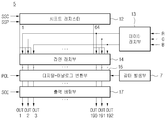
도 1은 종래의 액정표시장치를 개략적으로 도시한 블록도이고, 도 2는 도 1의 액정 패널을 회로적으로 도시한 도면이며, 도 3은 도 1의 데이터 드라이버를 상세하게 도시한 블록도이다.FIG. 1 is a block diagram schematically showing a conventional liquid crystal display device, FIG. 2 is a circuit diagram of the liquid crystal panel of FIG. 1, and FIG. 3 is a block diagram showing the data driver of FIG. 1 in detail .
도 1에 도시된 바와 같이, 종래의 액정표시장치는, 매트릭스 형태로 배열된 다수의 화소들을 갖는 액정 패널(9)과, 상기 액정 패널(9)에 스캔 신호를 공급하는 게이트 드라이버(3)와, 감마 전압을 발생하는 감마 발생부(7)와, 화상을 구성하는 R, G, B 데이터 신호에 상응하는 상기 감마 전압을 반영한 데이터 전압을 상기 액정 패널(9)에 공급하는 데이터 드라이버(5)와, 상기 액정 패널(9)로 공급하기 위한 공통 전압(Vcom)을 생성하는 공통전압 발생부(8)와, 상기 게이트 드라이버(3)와 상기 데이터 드라이버(5)를 제어하기 위한 제어 신호를 생성하는 타이밍 콘트롤러(1)를 포함한다.1, a conventional liquid crystal display device includes a
상기 액정 패널(9)은 다양한 모드에 따라 구조가 상이하다. 도 1에 도시된 상기 액정 패널은 IPS(In-Plane Switching) 모드이다.The
도 2에 도시된 바와 같이, 상기 액정 패널(9)은 다수의 게이트 라인(G1 내지 Gn)과 다수의 데이터 라인(D1 내지 Dm)이 교차 배열된다. 상기 게이트 라인(G1 내지 Gn)과 상기 데이터 라인(D1 내지 Dm)의 교차에 의해 화소(P)가 정의된다. 상기 화소(P)에는 상기 게이트 라인(G1 내지 Gn)과 상기 데이터 라인(D1 내지 Dm)에 연결된 박막트랜지스터(TFT)와 상기 박막트랜지스터(TFT)에 연결된 화소전극(미도시)이 형성된다. 상기 각 게이트 라인(G1 내지 Gn)과 평행하게 다수의 공통라인(VL1 내지 VLn)이 배열된다.As shown in FIG. 2, the
상기 화소전극에는 데이터 전압이 공급되고 상기 공통라인(VL1 내지 VLn)에는 공통 전압(Vcom)이 공급된다. 상기 화소전극과 상기 공통라인(VL1 내지 VLn) 사이에는 상기 데이터 전압과 상기 공통 전압(Vcom)의 차이에 해당하는 전위차가 발생한다. 상기 전위차에 의해 상기 화소 전극과 상기 공통라인(VL1 내지 VLn) 사이에는 존재하는 액정들이 구동하게 된다. 이러한 경우, 상기 액정들에 액정셀(Clc)이 형성된다. 도면에는 도시되지 않았지만, 상기 화소에 공급된 데이터 전압이 한 프레임 동안 유지되도록 하기 위한 스토리지 캐패시턴스가 상기 게이트 라인(G1 내지 Gn)과 상기 화소전극 사이에 형성될 수 있다.A data voltage is supplied to the pixel electrodes and a common voltage Vcom is supplied to the common lines VL1 to VLn. A potential difference corresponding to the difference between the data voltage and the common voltage Vcom is generated between the pixel electrode and the common lines VL1 to VLn. The liquid crystal molecules existing between the pixel electrode and the common lines VL1 to VLn are driven by the potential difference. In this case, the liquid crystal cell Clc is formed in the liquid crystal. Although not shown in the figure, storage capacitances may be formed between the gate lines G1 to Gn and the pixel electrodes so that the data voltage supplied to the pixels is maintained for one frame.
상기 타이밍 콘트롤러(1)는 외부의 비디오 카드 등으로부터 입력되는 영상 데이터 및 동기신호를 이용하여 상기 액정 패널(9)을 구동시키기 위한 제어신호를 생성한다. 상기 제어신호는 상기 게이트 드라이버(3)를 제어하는 제1 제어신호와 상기 데이터 드라이버(5)를 제어하는 제2 제어신호를 포함한다. 상기 제1 제어신호는 GSC(Gate shift Clock), GSP(Gate Start Pulse), GOE(Gate Output Enable) 등을 갖는다, 상기 제2 제어신호는 SSC(Source Shift Clock), SSP(Source Start Pulse), SOE(Source Output Enable), POL 등을 갖는다.The
상기 게이트 드라이버(3)는 상기 타이밍 콘트롤러(1)로부터 공급된 제1 제어신호에 응답하여 스캔 신호를 액정 패널의 각 게이트 라인(G1 내지 Gn)에 순차적으로 공급한다. 이에 따라, 상기 액정 패널(9)의 각 게이트 라인(G1 내지 Gn)은 순차적으로 활성화된다. 즉, 상기 각 게이트 라인(G1 내지 Gn) 상에 연결된 각 박막트랜지스터(TFT)가 턴-온되어 상기 박막트랜지스터(TFT)를 경유하여 신호가 지나갈 수 있다.The
이에 따라, 상기 데이터 드라이버(5)로부터 공급된 데이터 전압이 상기 활성화된 게이트 라인 상에 연결된 박막트랜지스터를 경유하여 화소전극으로 공급된다.Accordingly, the data voltage supplied from the
상기 데이터 드라이버(5)는 도 3에 도시된 바와 같이, 데이터 래치부(13), 시프트 레지스터(12), 라인 래치부(14), 디지털-아날로그 변환부(16) 및 출력 버퍼부(17) 등과 같은 다양한 구성요소들로 구성된다.3, the
상기 데이터 래치부(13)는 상기 타이밍 콘트롤러(1)로부터 공급된 n bit의 R, G, B 데이터 신호를 화소 단위로 래치한다. 상기 시프트 레지스터(12)는 SSP가 인가되는 경우 SSC에 동기하여 상기 데이터 래치부(13)에 래치된 R, G, B 데이터 신호를 라인 래치부(14)에 래치하기 위한 래치 인에이블 신호를 순차적으로 발생한다. 이와 같이 순차적으로 발생된 래치 인에이블 신호에 따라 상기 데이터 래치부(13)에 래치된 R, G, B 데이터 신호가 상기 라인 래치부(14)에 순차적으로 래치된다. The
상기 라인 래치부(14)는 설정된 채널 수에 상응하는 데이터 신호를 래치할 수 있다. 도 3의 상기 라인 래치부(14)는 192개의 채널 수에 대응된 데이터 신호를 래치할 수 있다.The
상기 디지털-아날로그 변환부(16)는 상기 라인 래치부(14)에 래치된 R, G, B 데이터 신호를 상기 감마 발생부(7)로부터 공급된 감마 전압에 상응하는 R, G, B 데이터 전압으로 변환한다. 상기 디지털-아날로그 변환부(16)는 POL에 따라 상기 감마 발생부(7)로부터 공급된 정극성(+) 감마 전압 또는 부극성(-) 감마 전압 중 어느 하나를 참조할 수 있다.The D /
상기 출력 버퍼부(17)는 SOE에 의해 상기 R, G, B 데이터 전압을 각 채널(OUT1 내지 OUT192)로 출력한다. 상기 각 채널은 상기 액정 패널(9)의 각 데이터 라인에 대응된다.The
한편, 상기 데이터 드라이버(5)는 상기 타이밍 콘트롤러(1)로 공급된 n 비트의 R, G, B 데이터 신호를 처리할 수 있다. On the other hand, the
하지만, 최근에는 프레임 레이트 제어(frame rate control) 방식을 이용하여 데이터 드라이버(5)에서 n 비트 이하의 R, G, B 데이터 신호를 타이밍 콘트롤러로부터 공급받아 n 비트 R, G, B 데이터 신호로 처리할 수 있는 액정표시장치가 개발되고 있다. 이에 따라, 데이터 드라이버(5)의 제품 단가를 줄일 수 있다.However, in recent years, the
예를 들어, 외부의 그래픽 카드에서 타이밍 콘트롤러(1)로 8비트의 R, G, B 데이터 신호가 공급되는 경우, 상기 타이밍 콘트롤러(1)에서 상위 6비트의 R, G, B 데이터와 하위 2비트의 R, G, B 데이터를 분리하고, 상위 6비트의 R, G, B 데이터를 바탕으로 프레임 레이트 제어 신호를 생성한다. For example, when 8-bit R, G, and B data signals are supplied from the external graphics card to the
따라서, 데이터 드라이버(5)는 타이밍 콘트롤러(1)에서 상위 6비트의 R, G, B 데이터를 받아 도 3에 도시된 구성에 의해 처리하고 프레임 레이트 제어 신호에 따라 프레임 처리를 수행하여 8비트의 R, G, B 데이터 신호로 복원할 수 있다. 이때, 8비트의 R, G, B 데이터 신호로 복원되기 위해서는 6비트의 상위 R, G, B 데이터 및 이보다 1계조 높은 6비트의 상위 R, G, B 데이터가 중 어느 하나 또는 반복적으로 4 프레임 동안 처리되어야 한다. 4프레임 동안, '6비트의 상위 R, G, B 데 이터가 세번 처리되고 1계조 높은(실질적으로는 4계조 높은) 6비트의 상위 R, G, B 데이터가 한번 처리되는 경우, 사람 눈에는 '01'의 데이터로 인식되고, 6비트의 상위 R, G, B 데이터와 1계조 높은 6비트의 R, G, B 데이터가 각각 2번씩 처리되는 경우, '10'으로 인식되며, 6비트의 상위 R, G, B 데이터가 한번 처리되고 1계조 높은 6비트의 상위 R, G, B 데이터가 세 번 처리되는 경우, '11'로 인식될 수 있다. Accordingly, the
만일 데이터 드라이버(5)는 6비트 처리 능력을 갖는데 반해, 타이밍 콘트롤러(1)로 10비트의 R, G, B 데이터가 공급되는 경우, 타이밍 콘트롤러(1)는 상위 6비트의 R, G, B 데이터 신호와 하위 4비트의 R, G, B 데이터 신호를 분리하고 상위 6비트의 R, G, B 데이터를 바탕으로 프레임 레이트 제어 신호를 생성한다. 따라서, 데이터 드라이버(5)는 상위 6비트의 R, G, B 데이터를 프레임 레이트 제어 신호에 따라 프레임 처리를 수행하여 10비트의 R, G, B 데이터 신호로 복원할 수 있다. 이때, 10비트의 R, G, B 데이터 신호로 복원되기 위해서는 6비트의 상위 R, G, B 데이터 및 이보다 1계조 높은 6비트의 상위 R, G, B 데이터 중 어느 하나를 이용하여 반복적으로 16 프레임 동안 처리되어야 한다.If 10 bits of R, G, and B data are supplied to the
따라서, 복원된 8비트의 R, G, B 데이터 신호는 4 프레임 동안 반복적으로 인버전되고, 복원된 10비트의 R, G, B 데이터 신호는 16 프레임 동안 반복적으로 인버전된다. Accordingly, the restored 8-bit R, G, and B data signals are repetitively reproduced for 4 frames, and the restored 10-bit R, G, and B data signals are repetitively reproduced for 16 frames.
도 4에 도시한 바와 같이, 종래의 프레임 레이트 제어 방식에서는 상위 6비트 R, G, B 데이터의 1계조 사이에 4 프레임 처리하여 3개의 계조가 추가될 수 있다.As shown in FIG. 4, in the conventional frame rate control method, three gradations can be added by processing four frames between one gradation of the upper 6 bits of R, G, and B data.
도 4에서 N는 상위 6비트 R, G, B 데이터의 계조를 나타낸다. 따라서, N이 1계조인 경우, 4계조(N*4)와 8계조((N+1)*4) 사이에 최대 3개의 계조가 추가될 수 있다.In FIG. 4, N represents the gradation of the upper 6 bits of R, G, and B data. Therefore, when N is 1, the maximum of 3 gradations can be added between the 4th gradation (N * 4) and the 8th gradation ((N + 1) * 4).
따라서, 현재의 프레임 레이트 제어 방식에서는 Vcom을 기준으로 4 프레임 동안 2개의 계조 밖에 사용할 수 없으므로, 이 2개의 계조를 프레임마다 번갈아 달리 출력하여 두 계조 사이에 3개의 계조를 표현할 수 있다.Therefore, in the current frame rate control system, since two gradations can be used for only four frames on the basis of Vcom, these two gradations can be alternately output for each frame to express three gradations between two gradations.
이와 같은 종래의 프레임 레이트 제어 방식에서는 비트수를 확장될 수록 프레임 수가 2m(m은 하위 비트수)으로 현저히 증가하게 되어, 결국 프레임(또는 디더링) 노이즈가 발생되는 문제가 있다. In such a conventional frame rate control method, there is a problem that frame (or dithering) noise is generated as the number of frames is increased to 2 m (m is a lower bit number) as the number of bits is increased.
따라서, 본 발명은 프레임 제어 방식을 달리하여 프레임 노이즈를 줄이고 비트 수를 확장할 수 있는 데이터 변조 방법, 이를 구비한 액정표시장치 및 그 구동 방법을 제공함에 그 목적이 있다.Accordingly, it is an object of the present invention to provide a data modulation method capable of reducing frame noise and extending the number of bits by changing the frame control method, a liquid crystal display device having the same, and a driving method thereof.
본 발명의 제1 실시예에 따르면, 데이터 변조 방법은, n비트의 데이터 신호로부터 상위 m비트를 갖는 제1 데이터와 하위 (n-m)비트 데이터를 분리하는 단계; 및 상기 제1 데이터와 상기 제1 데이터보다 1계조 높은 제2 데이터를 바탕으로 프레임별로 정극성 데이터와 부극성 데이터를 생성하는 단계를 포함한다.According to a first embodiment of the present invention, a data modulation method includes: separating first data having upper m bits from lower (n-m) bit data from an n-bit data signal; And generating positive polarity data and negative polarity data for each frame on the basis of the first data and the second data one level higher than the first data.
본 발명의 제2 실시예에 따르면, 하나의 게이트 라인, 기수번째 데이터 라인 및 우수번째 데이터 라인에 의해 화소가 정의되고, 상기 화소는 상기 게이트 라인과 상기 기수번째 데이터 라인에 연결된 제1 박막트랜지스터, 상기 게이트 라인과 상기 우수번째 데이터 라인에 연결된 제2 박막트랜지스터 및 상기 제1 및 제2 박막트랜지스터 사이에 배치된 액정셀을 포함하는 액정패널을 구동하는 액정표시장치의 구동 방법은, n비트의 데이터 신호로부터 분리된 상위 m비트를 갖는 제1 데이터와 상기 제1 데이터보다 1계조 높은 제2 데이터를 바탕으로 프레임별로 정극성 데이터와 부극성 데이터를 생성하는 단계; 및 상기 정극성 데이터에 상응하는 정극성 데이터 전압과 상기 부극성 데이터에 상응하는 부극성 데이터 전압을 상기 기수번째 데이터 라인과 상기 우수번째 데이터 라인에 프레임별로 교대로 공급하는 단계를 포함한다.According to a second embodiment of the present invention, a pixel is defined by one gate line, an odd-numbered data line and an even-numbered data line, and the pixel includes a first thin film transistor connected to the gate line and the odd- A driving method of a liquid crystal display driving a liquid crystal panel including a second thin film transistor connected to the gate line and the odd data line and a liquid crystal cell arranged between the first thin film transistor and the second thin film transistor, Generating positive polarity data and negative polarity data for each frame based on first data having higher m bits separated from the signal and second data higher than the first data by one level; And alternately supplying a positive polarity data voltage corresponding to the positive polarity data and a negative polarity data voltage corresponding to the negative polarity data to the odd-numbered data line and the even-numbered data line on a frame-by-frame basis.
본 발명의 제3 실시예에 따르면, 액정표시장치는, 하나의 게이트 라인, 기수번째 데이터 라인 및 우수번째 데이터 라인에 의해 화소가 정의되고, 상기 화소는 상기 게이트 라인과 상기 기수번째 데이터 라인에 연결된 제1 박막트랜지스터, 상기 게이트 라인과 상기 우수번째 데이터 라인에 연결된 제2 박막트랜지스터 및 상기 제1 및 제2 박막트랜지스터 사이에 배치된 액정셀을 포함하는 액정패널; n비트의 데이터 신호로부터 분리된 상위 m비트를 갖는 제1 데이터와 상기 제1 데이터보다 1계조 높은 제2 데이터를 바탕으로 프레임별로 정극성 데이터와 부극성 데이터를 생성하는 타이밍 콘트롤러; 및 상기 정극성 데이터에 상응하는 정극성 데이터 전압과 상기 부극성 데이터에 상응하는 부극성 데이터 전압을 상기 기수번째 데이 터 라인과 상기 우수번째 데이터 라인에 프레임별로 교대로 공급하는 데이터 드라이버를 포함한다.According to the third embodiment of the present invention, a liquid crystal display device is characterized in that a pixel is defined by one gate line, an odd-numbered data line and an even-numbered data line, and the pixel is connected to the gate line and the odd- A liquid crystal panel including a first thin film transistor, a second thin film transistor connected to the gate line and the odd data line, and a liquid crystal cell disposed between the first thin film transistor and the second thin film transistor; a timing controller for generating positive polarity data and negative polarity data for each frame on the basis of first data having upper m bits separated from the n-bit data signal and second data higher than the first data by one level; And a data driver for alternately supplying positive polarity data voltages corresponding to the positive polarity data and negative polarity data voltages corresponding to the negative polarity data frame by frame to the odd-numbered data line and the even-numbered data line.
본 발명은 프레임 레이트 제어에 따라 계조를 표현함으로써, 데이터 드라이버의 처리 비트수를 줄일 수 있으므로, 데이터 드라이버의 제품 단가를 절감할 수 있다.According to the present invention, by expressing the gradation according to the frame rate control, the number of processed bits of the data driver can be reduced, so that the product cost of the data driver can be reduced.
본 발명은 공통전압을 사용하지 않는 대신 정극성 감마 전압과 부극성 감마 전압 사이의 차이를 이용하여 프레임 레이트 변조함으로써, 프레임 수가 종래에 비해 적어도 절반 이하로 줄어들어 프레임 노이즈를 현저히 줄일 수 있다. The present invention can reduce the frame noise significantly by reducing the number of frames by at least half compared with the conventional technique by using the difference between the positive gamma voltage and the negative gamma voltage to perform frame rate modulation instead of using the common voltage.
이하, 첨부된 도면을 참조하여 본 발명의 실시예를 설명한다.Hereinafter, embodiments of the present invention will be described with reference to the accompanying drawings.
도 5는 본 발명의 제1 실시예에 따른 프레임 레이트 제어 방식을 개념적으로 설명한 도면이다.5 is a diagram conceptually illustrating a frame rate control method according to the first embodiment of the present invention.
본 발명의 제1 실시예는 공통전압(Vcom)을 사용하지 않는 액정표시장치에 적용될 수 있다.The first embodiment of the present invention can be applied to a liquid crystal display device which does not use the common voltage Vcom.
본 발명의 제1 실시예는 정극성 감마 곡선과 부극성 감마 곡선이 서로 대칭되는 것으로 한정한다. The first embodiment of the present invention defines that the positive gamma curve and the negative gamma curve are symmetrical to each other.
도 5에 도시한 바와 같이, 8비트의 R, G, B 데이터 신호 각각에서 상위 6비트 데이터의 제1 및 제2 계조(N*4, (N+1)*4) 사이에 3개의 계조(N*4+1, N*4+2, N*4+3, 이하 "제1 추가 계조, 제2 추가 계조 및 제3 추가 계조"라 함)를 추가할 수 있다. 상위 6비트의 데이터는 데이터 드라이버에서 처리될 수 있다. (N + 4) and (N + 1) * 4) of the upper 6-bit data in 8-bit R, G and B data signals, N * 4 + 1, N * 4 + 2, N * 4 + 3, hereinafter referred to as "first additional gray level, second additional gray level and third additional gray level"). The upper 6 bits of data can be processed in the data driver.
상기 제1 계조(N*4)는 상위 6비트 데이터를 정극성과 부극성으로 처리하여 정극성 상위 6비트 데이터(P2)에 상응하는 아날로그 데이터 전압(2.5V)과 부극성 상위 6비트 데이터(P1)에 상응하는 아날로그 데이터 전압(2.1V) 사이의 차이값(0.4V)으로 결정될 수 있다. 정극성 상위 6비트 데이터(P2)의 비트값과 부극성 상위 6비트 데이터(P1)의 비트값은 동일할 수 있다. 하지만, 정극성 상위 6비트 데이터(P2)에 상응하는 아날로그 데이터 전압(2.5V)과 부극성 상위 6비트 데이터(P1)에 상응하는 아날로그 데이터 전압(2.1V)은 상이할 수 있다. The first gradation N * 4 processes the upper 6-bit data to positive and negative polarities so that the analog data voltage (2.5V) corresponding to the upper 6-bit data P2 and the upper 6-bit data P1 (0.4 V) between the analog data voltage (2.1 V) corresponding to the analog data voltage (2.1 V). The bit value of the positive 6-bit data P2 and the bit value of the negative 6-bit data P1 may be the same. However, the analog data voltage (2.5V) corresponding to the high-order 6-bit data (P2) and the analog data voltage (2.1V) corresponding to the high-order 6-bit data (P1) may be different.
예를 들어, 상위 6비트 데이터가 '000001'인 경우, 정극성 상위 6비트 데이터(P2)와 부극성 상위 6비트 데이터(P1) 또한 '000001'이다. 'For example, when the high-order 6-bit data is '000001', the high-order 6-bit data P2 and the high-order 6-bit data P1 are also '000001'. '
제2 계조((N+1)*4)는 상위 6비트 데이터를 정극성과 부극성으로 처리하여 정극성 상위 6비트 데이터(P4)에 상응하는 아날로그 데이터 전압(2.6V)과 부극성 상위 6비트 데이터(P3)에 상응하는 아날로그 데이터 전압(2.0V) 사이의 차이값(0.6V)으로 결정될 수 있다. 정극성 상위 6비트 데이터(P4)의 비트값과 부극성 상위 6비트 데이터(P3)의 비트값은 동일할 수 있다. 하지만, 정극성 상위 6비트 데이터(P4)에 상응하는 아날로그 데이터 전압(2.6V)과 부극성 상위 6비트 데이터(P3)에 상응하는 아날로그 데이터 전압(2.0V)은 상이할 수 있다.The second gradation ((N + 1) * 4) processes the upper 6-bit data in the positive polarity and the negative polarity so that the analog data voltage (2.6V) corresponding to the upper 6-bit data P4 (0.6 V) between the analog data voltage (2.0 V) corresponding to the data P3. The bit value of the positive six-bit data P4 and the bit value of the negative six-bit data P3 may be the same. However, the analog data voltage (2.6 V) corresponding to the positive 6-bit data P4 and the analog data voltage (2.0 V) corresponding to the negative 6-bit data P3 may be different.
예를 들어, 상위 6비트 데이터가 '000010'인 경우, 정극성 상위 6비트 데이터(P4)와 부극성 상위 6비트 데이터(P3) 또한 '000010'이다. 'For example, when the upper 6-bit data is '000010', the positive 6-bit data P4 and the negative 6-bit data P3 are also '000010'. '
여기서, 각 아날로그 데이터 전압은 정극성 감마 곡선에 따라 생성된 정극성 감마 전압들과 부극성 감마 곡선에 따라 생성된 부극성 감마 전압들일 수 있다. Here, each analog data voltage may be positive gamma voltages generated according to a positive gamma curve and negative gamma voltages generated according to a negative gamma curve.
제1 내지 제3 추가 계조(N*4+1, N*4+2, N*4+3) 중에서, 제2 추가 계조(N*4+2)는 제1 계조(N*4)와 제2 계조((N+1)*4)를 이용하여 직접 결정될 수 있다. 즉, 제2 추가 계조(N*4+2)는 제1 계조(N*4)의 정극성 상위 6비트 데이터(P2)에 상응하는 아날로그 데이터 전압(2.5V)과 제2 계조((N+1)*4)의 부극성 상위 6비트 데이터(P3)에 상응하는 아날로그 데이터 전압(2.0V) 사이의 차이값(0.5V)으로 결정될 수 있다. The second additional gray level N * 4 + 2 is set to the first gray level N * 4 and the second gray level N * 4 + 2 from among the first to third additional gray levels N * 4 + 1, N * 4 + 2 (N + 1) * 4). That is, the second additional gray level N * 4 + 2 corresponds to the analog data voltage 2.5V corresponding to the positive six bit data P2 of positive polarity of the first gray level N * 4 and the second gray level N + (0.5 V) between the analog data voltage (2.0 V) corresponding to the negative high-order 6-bit data (P3) of the negative polarity bit data (* 1) * 4.
도 5에 도시되지 않았지만, 본 발명의 제1 실시예는 정극성 감마 곡선과 부극성 감마 곡선이 서로 대칭되므로, 제2 추가 계조(N*4+2)는 제1 계조(N*4)의 부극성 상위 6비트 데이터(P1)에 상응하는 아날로그 데이터 전압(2.1V)과 제2 계조((N+1)*4)의 정극성 상위 6비트 데이터(P4)에 상응하는 아날로그 데이터 전압(2.6V) 사이의 차이값(0.5V)으로 결정될 수도 있다. Although not shown in FIG. 5, in the first embodiment of the present invention, since the positive gamma curve and the negative gamma curve are symmetrical to each other, the second additional gradation N * 4 + 2 corresponds to the first gradation N * The analog data voltage 2.6 (corresponding to the positive six-bit data P4) of the analog data voltage 2.1V corresponding to the negative high-order bit data P1 and the positive high-order 6-bit data P4 of the second gradation N + (V).
제1 추가 계조(N*4+1)는 제1 계조(N*4)와 제2 추가 계조(N*4+2) 사이에서 프레임 레이트 변조(또는 디더링이라 함)에 의해 산출되고, 제3 추가 계조(N*4+3)는 제2 추가 계조(N*4+2)와 제2 계조((N+1)*4) 사이에서 프레임 레이트 변조에 의해 산출될 수 있다.The first additional gray level N * 4 + 1 is calculated by frame rate modulation (or dithering) between the first gray level N * 4 and the second additional gray level N * 4 + 2, The additional gradation N * 4 + 3 can be calculated by frame rate modulation between the second additional gradation N * 4 + 2 and the second gradation (N + 1) * 4.
예를 들어, 제1 추가 계조(N*4+1)는 제1 프레임에 제1 계조(N*4)가 출력되고 제2 프레임에 제2 추가 계조(N*4+2)가 출력되어 얻어질 수 있다. 제3 추가 계조(N*4+3)는 제1 프레임에 제2 추가 계조(N*4+2)가 출력되고 제2 프레임에 제2 계조((N+1)*4)가 출력되어 얻어질 수 있다. For example, in the first additional gray level N * 4 + 1, the first gray level N * 4 is output to the first frame and the second additional gray level N * 4 + 2 is output to the second frame Can be. The third additional gray level N * 4 + 3 outputs the second additional gray level N * 4 + 2 to the first frame and the second gray level N + 1 * 4 to the second frame Can be.
따라서, 본 발명의 제1 실시예에 따르면, 제1 계조(N*4)와 제2 계조((N+1)*4) 사이의 3개의 계조, 즉 제1 내지 제3 추가 계조(N*4+1, N*4+2, N*4+3) 중 제2 추가 계조(N*4+2)는 제1 계조(N*4)와 제2 계조((N+1)*4)를 이용하여 결정되는 실제 데이터이다. 그러므로, 제1 및 제3 추가 계조(N*4+1, N*4+3)만 제1 계조(N*4)와 제2 추가 계조(N*4+2) 그리고 제2 추가 계조(N*4+2)와 제2 계조((N+1)*4)를 프레임 레이트 변조하여 산출하면 되므로, 2개의 프레임에 의해 제1 및 제3 추가 계조(N*4+1, N*4+3)가 산출될 수 있다. 종래에 4개의 프레임에 의해 상위 6비트의 두 계조 사이에 3개의 추가 계조를 산출하는 것에 비해 프레임 수가 반으로 줄게 되어, 프레임 노이즈(또는 디더링) 노이즈가 현저히 줄어들 수 있다.Therefore, according to the first embodiment of the present invention, three gradations between the first gradation N * 4 and the second gradation (N + 1) * 4, that is, the first to third additional gradations N * The second additional gray level N * 4 + 2 among the first gray level N * 4 and the second gray level N + 4 * 2 among the first gray level N * 4 + 1, N * As shown in FIG. Therefore, only the first and third additional gradations N * 4 + 1 and N * 4 + 3 are divided into the first gradation N * 4 and the second additional gradation N * 4 + 4 + 2) and the second gradation (N + 1) * 4 can be calculated by frame-rate modulating the first and third additional gradations N * 4 + 1 and N * 4 + 3) can be calculated. Conventionally, the number of frames is reduced by half in comparison with the case where three additional gradations are calculated between two gradations of the upper 6 bits by four frames, and frame noise (or dithering) noise can be remarkably reduced.
한편, 10비트의 데이터 신호이고 데이터 드라이버에서 6비트 데이터만 처리되는 경우, 제1 계조(N*4)와 제2 추가 계조(N*4+2) 사이에 4개의 추가 계조가 프레임 레이트 변조에 의해 산출되고, 제2 추가 계조(N*4+2)와 제2 계조((N+1)*4) 사이에 4개의 추가 계조가 프레임 레이트 변조에 의해 산출될 수 있다. 이러한 경우, 총 8개의 추가 계조가 산출되어야 하는데, 이들 추가 계조를 산출하기 위해서는 8개의 프레임이 사용될 수 있다. 이 또는 종래의 16개의 프레임을 사용하는 것이 비해 반으로 줄게 되어, 프레임 노이즈(또는 디더링) 노이즈가 현저히 줄어들 수 있다.On the other hand, when only the 6-bit data is processed by the data driver and the data driver is a 10-bit data signal, four additional gradations between the first gradation N * 4 and the second additional gradation N * 4 + , And four additional gradations between the second additional gradation (N * 4 + 2) and the second gradation (N + 1) * 4 can be calculated by frame rate modulation. In this case, a total of eight additional tones should be calculated, and eight frames may be used to calculate these additional tones. The frame noise (or dithering) noise can be remarkably reduced, as compared with the case of using the conventional or 16 conventional frames.
도 6은 본 발명의 제1 실시예에 따른 프레임 레이트 제어 방식의 알고리즘을 도시한 도면이다.6 is a diagram illustrating an algorithm of the frame rate control method according to the first embodiment of the present invention.
도 6에서, 상위 6비트 데이터의 각 계조(N*4, (N+1)*4)와 각 계조를 이용하 여 결정된 제2 추가 계조(N*4+2)는 디더링에 관계없이 얻어진 고정 전압이고, 이들 고정 전압을 이용하여 프레임 레이트 변조에 의해 디더링값(N*4+1, N*4+3 등)이 얻어질 수 있다.6, the gradation (N * 4, (N + 1) * 4) of the upper 6-bit data and the second additional gradation N * 4 + 2 determined using each gradation , And dither values (N * 4 + 1, N * 4 + 3, etc.) can be obtained by frame rate modulation using these fixed voltages.
도6에 도시한 바와 같이, 데이터 드라이버가 6비트 데이터를 처리할 때, 2비트 확장하는 경우, 즉 외부의 그래픽 카드에서 8비트 데이터 신호가 입력되는 경우에는 2개의 프레임(2FRC)에 의해 디더링값들이 얻어지고, 4비트 확장하는 경우, 즉 외부의 그래픽 카드에서 10비트 데이터 신호가 입력되는 경우에는 8개의 프레임(*FRC)에 의해 디더링값들이 얻어질 수 있다.As shown in FIG. 6, when the data driver processes 6-bit data and expands by 2 bits, that is, when an 8-bit data signal is input from an external graphics card, the 2-frame (2FRC) Dithering values can be obtained by eight frames (* FRC) when four bits are expanded, that is, when a 10-bit data signal is input from an external graphics card.
본 발명의 제1 실시예에 의해 종래에 비해 프레임 개수를 반으로 줄여, 프레임 노이즈를 현저히 줄일 수 있다.According to the first embodiment of the present invention, the number of frames can be reduced by half in comparison with the prior art, and the frame noise can be remarkably reduced.
도 7은 본 발명의 제2 실시예에 따른 프레임 레이트 제어 방식을 개념적으로 설명한 도면이다.FIG. 7 is a diagram conceptually illustrating a frame rate control method according to the second embodiment of the present invention.
본 발명의 제2 실시예는 공통전압(Vcom)을 사용하지 않는 액정표시장치에 적용될 수 있다.The second embodiment of the present invention can be applied to a liquid crystal display device which does not use the common voltage Vcom.
본 발명의 제2 실시예는 정극성 감마 곡선과 부극성 감마 곡선이 서로 비대칭되는 것으로 한정한다. 이때, 정극성 감마 곡선과 부극성 감마 곡선은 그 기울기의 비가 1: 3 또는 3: 1일 수 있다. 예를 들어, 정극성 감마 곡선의 기울기는 부극성 감마 곡선의 기울기의 3배일 수 있다. 또는 부극성 감마 곡선의 기울기는 정극성 감마 곡선의 기울기의 3배일 수 있다.The second embodiment of the present invention defines that the positive gamma curve and the negative gamma curve are asymmetric with respect to each other. At this time, the positive gamma curve and the negative gamma curve may have a slope ratio of 1: 3 or 3: 1. For example, the slope of the positive gamma curve may be three times the slope of the negative gamma curve. Or the slope of the negative gamma curve may be three times the slope of the positive gamma curve.
도 7은 부극성 감마 곡선의 기울기가 정극성 감마 곡선의 기울기의 3배 큰 것을 도시한 것이다.7 shows that the slope of the negative gamma curve is three times larger than the slope of the positive gamma curve.
도 7에 도시한 바와 같이, 8비트의 R, G, B 데이터 신호 각각에서 상위 6비트 데이터의 제1 및 제2 계조(N*4, (N+1)*4) 사이에 3개의 계조(N*4+1, N*4+2, N*4+3, 이하 "제1 추가 계조, 제2 추가 계조 및 제3 추가 계조"라 함)를 추가할 수 있다. 상위 6비트의 데이터는 데이터 드라이버에서 처리될 수 있다. (N + 4) and (N + 1) * 4) of the upper 6-bit data in 8-bit R, G and B data signals, N * 4 + 1, N * 4 + 2, N * 4 + 3, hereinafter referred to as "first additional gray level, second additional gray level and third additional gray level"). The upper 6 bits of data can be processed in the data driver.
상기 제1 계조(N*4)는 상위 6비트 데이터를 정극성과 부극성으로 처리하여 정극성 상위 6비트 데이터(Q2)에 상응하는 아날로그 데이터 전압(2.5V)과 부극성 상위 6비트 데이터(Q1)에 상응하는 아날로그 데이터 전압(2.1V) 사이의 차이값(0.4V)으로 결정될 수 있다. 정극성 상위 6비트 데이터(Q2)의 비트값과 부극성 상위 6비트 데이터(Q1)의 비트값은 동일할 수 있다. 하지만, 정극성 상위 6비트 데이터(Q2)에 상응하는 아날로그 데이터 전압(2.5V)과 부극성 상위 6비트 데이터(Q1)에 상응하는 아날로그 데이터 전압(2.1V)은 상이할 수 있다. The first gradation N * 4 processes the upper 6-bit data to positive and negative polarities and outputs the analog data voltage (2.5V) corresponding to the upper 6-bit data Q2 of positive polarity and the upper 6-bit data Q1 (0.4 V) between the analog data voltage (2.1 V) corresponding to the analog data voltage (2.1 V). The bit value of the high-order 6-bit data (Q2) and the bit value of the negative high-order 6-bit data (Q1) may be the same. However, the analog data voltage (2.5 V) corresponding to the high-order 6-bit data (Q2) and the analog data voltage (2.1 V) corresponding to the high-order 6-bit data (Q1) may be different.
예를 들어, 상위 6비트 데이터가 '000001'인 경우, 정극성 상위 6비트 데이터(Q2)와 부극성 상위 6비트 데이터(Q1) 또한 '000001'이다. 'For example, when the upper 6-bit data is '000001', the positive 6-bit data Q2 and the negative 6-bit data Q1 are also '000001'. '
제2 계조((N+1)*4)는 상위 6비트 데이터를 정극성과 부극성으로 처리하여 정극성 상위 6비트 데이터(Q4)에 상응하는 아날로그 데이터 전압(2.6V)과 부극성 상위 6비트 데이터(Q3)에 상응하는 아날로그 데이터 전압(1.8V) 사이의 차이값(0.8V)으로 결정될 수 있다. 정극성 상위 6비트 데이터(Q4)의 비트값과 부극성 상위 6비트 데이터(Q3)의 비트값은 동일할 수 있다. 하지만, 정극성 상위 6비트 데이터(Q4)에 상응하는 아날로그 데이터 전압(2.6V)과 부극성 상위 6비트 데이터(Q3)에 상응 하는 아날로그 데이터 전압(1.8V)은 상이할 수 있다.The second gradation ((N + 1) * 4) processes the upper 6-bit data in the positive polarity and the negative polarity so that the analog data voltage (2.6V) corresponding to the upper 6-bit data (Q4) (0.8 V) between the analog data voltage (1.8 V) corresponding to the data (Q3). The bit value of the high-order 6-bit data (Q4) and the bit value of the negative high-order 6-bit data (Q3) may be the same. However, the analog data voltage (2.6V) corresponding to the high-order 6-bit data (Q4) and the analog data voltage (1.8V) corresponding to the high-order 6-bit data (Q3) may be different.
예를 들어, 상위 6비트 데이터가 '000010'인 경우, 정극성 상위 6비트 데이터(Q4)와 부극성 상위 6비트 데이터(Q3) 또한 '000010'이다. For example, when the upper 6-bit data is '000010', the positive 6-bit data Q4 and the negative 6-bit data Q3 are also '000010'.
여기서, 각 아날로그 데이터 전압은 정극성 감마 곡선에 따라 생성된 정극성 감마 전압들과 부극성 감마 곡선에 따라 생성된 부극성 감마 전압들일 수 있다. Here, each analog data voltage may be positive gamma voltages generated according to a positive gamma curve and negative gamma voltages generated according to a negative gamma curve.
제1 내지 제3 추가 계조(N*4+1, N*4+2, N*4+3) 중에서, 제1 및 3 추가 계조(N*4+1, N*4+3)는 제1 계조(N*4)와 제2 계조((N+1)*4)를 이용하여 직접 결정될 수 있다. 즉, 제1 추가 계조(N*4+1)는 제1 계조(N*4)의 부극성 상위 6비트 데이터(Q1)에 상응하는 아날로그 데이터 전압(2.1V)과 제2 계조((N+1)*4)의 정극성 상위 6비트 데이터(Q4)에 상응하는 아날로그 데이터 전압(2.6V) 사이의 차이값(0.5V)으로 결정될 수 있다. 제3 추가 계조(N*4+3)는 제1 계조(N*4)의 정극성 상위 6비트 데이터(Q2)에 상응하는 아날로그 데이터 전압(2.5V)과 제2 계조((N+1)*4)의 부극성 상위 6비트 데이터(Q3)에 상응하는 아날로그 데이터 전압(1.8V) 사이의 차이값(0.7V)으로 결정될 수 있다. Of the first to third additional gradations (N * 4 + 1, N * 4 + 2, N * 4 + 3), the first and third additional gradations N * 4 + 1, N * 4 + Can be directly determined using the gradation (N * 4) and the second gradation (N + 1) * 4. That is, the first additional gray level N * 4 + 1 is the analog data voltage (2.1V) corresponding to the negative six bit data Q1 of the first gray level N * 4 and the second gray level (N + (0.5 V) between the analog data voltage (2.6 V) corresponding to the high-order 6-bit data (Q4) of the positive polarity bit data (* 4) The third additional gray level N * 4 + 3 is the sum of the analog data voltage 2.5V corresponding to the positive six bit data Q2 of the first gray level N * 4 and the second gray level N + (0.7 V) between the analog data voltage (1.8 V) corresponding to the negative high-order 6-bit data (Q3) of the negative polarity data * 4.
제2 추가 계조(N*4+2)는 제1 추가 계조(N*4+1)와 제3 추가 계조(N*4+3) 사이에서 프레임 레이트 변조에 의해 산출될 수 있다. The second additional tone N * 4 + 2 can be calculated by frame rate modulation between the first additional tone N * 4 + 1 and the third additional tone N * 4 + 3.
예를 들어, 제1 프레임에 제1 추가 계조(N*4+1)가 출력되고 제2 프레임에 제3 추가 계조(N*4+3)가 출력되어 얻어질 수 있다.For example, a first additional gray level N * 4 + 1 may be output in the first frame and a third additional gray level N * 4 + 3 may be output in the second frame.
따라서, 본 발명의 제1 실시예에 따르면, 제1 계조(N*4)와 제2 계조((N+1)*4) 사이의 3개의 계조, 즉 제1 내지 제3 추가 계조(N*4+1, N*4+2, N*4+3) 중 제1 및 제3 추가 계조(N*4+1, N*4+3)는 제1 계조(N*4)와 제2 계조((N+1)*4)를 이용하여 결정되는 실제 데이터이다. 그러므로, 제2 추가 계조(N*4+2)만 제1 추가 계조(N*4+1)와 제3 추가 계조(N*4+3)를 프레임 레이트 변조하여 산출하면 되므로, 2개의 프레임에 의해 제2 추가 계조(N*4+2)가 산출될 수 있다. 종래에 4개의 프레임에 의해 상위 6비트의 두 계조 사이에 3개의 추가 계조를 산출하는 것에 비해 프레임 수가 반으로 줄게 되어, 프레임 노이즈(또는 디더링) 노이즈가 현저히 줄어들 수 있다.Therefore, according to the first embodiment of the present invention, three gradations between the first gradation N * 4 and the second gradation (N + 1) * 4, that is, the first to third additional gradations N * The first and third additional gray levels N * 4 + 1 and N * 4 + 3 among the first gray level N * 4 and the second gray level N * ((N + 1) * 4). Therefore, since only the second additional gray level N * 4 + 2 is calculated by frame rate modulating the first additional gray level N * 4 + 1 and the third additional gray level N * 4 + 3, The second additional gray level N * 4 + 2 can be calculated. Conventionally, the number of frames is reduced by half in comparison with the case where three additional gradations are calculated between two gradations of the upper 6 bits by four frames, and frame noise (or dithering) noise can be remarkably reduced.
한편, 10비트의 데이터 신호이고 데이터 드라이버에서 6비트 데이터만 처리되는 경우, 제1 계조(N*4)와 제1 추가 계조(N*4+1) 사이에 2개의 추가 계조가 프레임 레이트 변조에 의해 산출되고, 제1 추가 계조(N*4+1)와 제3 추가 계조(N*4+3) 사이에 4개의 추가 계조가 프레임 레이트 변조에 의해 산출되며, 제3 추가 계조(N*4+3)와 제2 계조((N+1)*4) 사이에 2개의 추가 계조가 프레임 레이트 변조에 의해 산출될 수 있다. 이러한 경우, 총 8개의 추가 계조가 산출되어야 하는데, 이들 추가 계조를 산출하기 위해서는 4개의 프레임이 사용될 수 있다. 이 또는 종래의 16개의 프레임을 사용하는 것이 비해 1/4로 줄게 되어, 프레임 노이즈(또는 디더링) 노이즈가 현저히 줄어들 수 있다.On the other hand, when only the 6-bit data is processed by the data driver and the data driver is a 10-bit data signal, two additional gradations between the first gradation N * 4 and the first additional gradation N * 4 + Four additional gradations between the first additional gradation N * 4 + 1 and the third additional gradation N * 4 + 3 are calculated by frame rate modulation, and the third additional gradation N * 4 + +3) and the second gradation ((N + 1) * 4) can be calculated by frame rate modulation. In this case, a total of eight additional tones should be calculated, and four frames may be used to calculate these additional tones. The frame noise (or dithering) noise can be remarkably reduced.
도 8은 본 발명의 제2 실시예에 따른 프레임 레이트 제어 방식의 알고리즘을 도시한 도면이다.8 is a diagram illustrating an algorithm of the frame rate control method according to the second embodiment of the present invention.
도 8에서, 상위 6비트 데이터의 각 계조(N*4, (N+1)*4)와 각 계조를 이용하여 결정된 제1 및 제2 추가 계조(N*4+1, N*4+2)는 디더링에 관계없이 얻어진 고정 전압이고, 이들 고정 전압을 이용하여 프레임 레이트 변조에 의해 디더링값(N*4+2 등)이 얻어질 수 있다.8, the first and second additional gray levels N * 4 + 1 and N * 4 + 2 (N * 4 + ) Is a fixed voltage obtained regardless of dithering, and a dithering value (N * 4 + 2, etc.) can be obtained by frame rate modulation using these fixed voltages.
도 8에 도시한 바와 같이, 데이터 드라이버가 6비트 데이터를 처리할 때, 2비트 확장하는 경우, 즉 외부의 그래픽 카드에서 8비트 데이터 신호가 입력되는 경우에는 2개의 프레임에 의해 디더링값들이 얻어지고(2FRC라 함), 4비트 확장하는 경우, 즉 외부의 그래픽 카드에서 10비트 데이터 신호가 입력되는 경우에는 4개의 프레임에 의해 디더링값들이 얻어질 수 있다(4RFC라 함). As shown in FIG. 8, when the data driver processes 6-bit data and expands by 2 bits, that is, when an 8-bit data signal is input from an external graphics card, dithering values are obtained by two frames (2FRC), and when a 4-bit extension is performed, that is, when a 10-bit data signal is input from an external graphics card, dithering values can be obtained by 4 frames (referred to as 4RFC).
본 발명의 제1 실시예에 의해 종래에 비해 프레임 개수를 반으로 줄여, 프레임 노이즈를 현저히 줄일 수 있다.According to the first embodiment of the present invention, the number of frames can be reduced by half in comparison with the prior art, and the frame noise can be remarkably reduced.
도 9는 본 발명의 제1 및 제2 실시예에 따른 프레임 레이트 제어 방식을 적용한 액정표시장치를 도시한 블록도이다.9 is a block diagram illustrating a liquid crystal display device to which a frame rate control method according to the first and second embodiments of the present invention is applied.
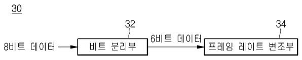
도 9를 참조하면, 액정표시장치(20)는 타이밍 콘트롤러(30), 게이트 드라이버(40), 데이터 드라이버(50), 감마 발생부(60) 및 액정 패널(70)을 포함한다.9, the
상기 데이터 드라이버(50)는 6비트 데이터를 처리하고, 상기 타이밍 콘트롤러(30)에는 외부의 그래픽 카드로부터 8비트 R, G, B 데이터가 공급되는 것으로 한정하여 설명한다.The
상기 타이밍 콘트롤러(30)는 외부의 그래픽 카드로부터 영상을 표시하기 위한 8비트의 R, G, B 데이터 신호, 영상의 표시 타이밍을 제어하는 데이터 클럭신호(Dclk), 수직동기신호(Vsync) 및 수평동기신호(Hsync)를 공급받는다.The
상기 타이밍 콘트롤러(30)는 상기 데이터 클럭신호(Dclk), 수직동기신 호(Vsync) 및 수평동기신호(Hsync)를 바탕으로 게이트 드라이버를 구동하기 위한 제1 제어신호(GSP, GSC, GOE)와 데이터 드라이버(50)를 구동하기 위한 제2 제어신호(SSP, SSC, SOE)를 생성한다.The
상기 타이밍 콘트롤러(30)는 도 10에 도시한 바와 같이, 6비트 처리가 가능한 데이터 드라이버(50)에 부합하도록 8비트 R, G, B 데이터 신호를 변조하기 위해, 비트 분리부(32)와 프레임 레이트 변조부(34)를 포함한다.As shown in FIG. 10, the
상기 비트 분리부(32)는 8비트 R, G, B 데이터 신호로부터 상위 6비트 데이터와 하위 2비트 데이터로 분리한다.The
상기 프레임 레이트 변조부(34)는 상위 6비트 데이터를 2프레임 동안(이하, 제1 및 제2 프레임이라 함) 처리하여 8비트 데이터의 계조를 표현하도록 변조된다. 즉, 상기 프레임 레이트 변조부(34)는 상위 6비트 데이터(이하, 제1 상위 6비트 데이터라 함)와 이보다 1계조 높은 상위 6비트 데이터(이하, 제2 상위 6비트 데이터라 함)를 바탕으로 각 프레임 동안 정극성 데이터와 부극성 데이터를 갖도록 배열한다.The
상기 정극성 데이터는 제1 및 제2 상위 6비트 데이터 중 어느 하나일 수 있다. 또한, 상기 부극성 데이터는 제1 및 제2 상위 6비트 데이터 중 어느 하나일 수 있다.The positive polarity data may be any one of first and second high-order 6-bit data. The negative polarity data may be any one of first and second upper 6-bit data.
도 5에 도시한 바와 같이, 제1 상위 6비트 데이터의 계조(N*4, 이하, 제1 계조라 함)는 정극성 제1 상위 6비트 데이터(P2)와 부극성 제1 상위 6비트 데이터(P1)에 의해 결정될 수 있다. 즉, 나중에 설명되겠지만, 정극성 제1 상위 6비트 데이터(P2)에 상응하는 아날로그 데이터 전압(2. 5V)과 부극성 제1 상위 6비트 데이터(P1)에 상응하는 아날로그 데이터 전압(2.1V) 사이의 차이값(0.4V)에 의해 제1 계조(N*4)가 표현될 수 있다.5, the gradation (N * 4, hereinafter referred to as the first gradation) of the first higher-order 6-bit data is the first higher-order 6-bit data P2 and the first higher- (P1). ≪ / RTI > That is, as will be described later, the analog data voltage (2.1 V) corresponding to the first high-order 6-bit data (P2) and the negative first data 6 (P1) The first gradation N * 4 can be expressed by a difference value (0.4 V) between the first gradation N *
제2 상위 6비트 데이터의 계조((N+1)*4, 이하, 제2 계조라 함)는 정극성 제2 상위 6비트 데이터(P4)와 부극성 제2 상위 6비트 데이터(P3)에 의해 결정될 수 있다. 즉, 정극성 제2 상위 6비트 데이터(P4)에 상응하는 아날로그 데이터 전압(2.6V)과 부극성 제2 상위 6비트 데이터(P3)에 상응하는 아날로그 데이터 전압(2.0V) 사이의 차이값(0.6V)에 의해 제2 계조((N+1)*4)가 표현될 수 있다.(N + 1) * 4, hereinafter referred to as the second gradation) of the second upper 6-bit data is supplied to the positive second upper 6-bit data P4 and the negative second upper 6-bit data P3 Lt; / RTI > That is, the difference (+) between the analog data voltage (2.6V) corresponding to the second upper 6-bit data P4 and the analog data voltage (2.0V) corresponding to the second higher 6-bit data P3 The second gray level ((N + 1) * 4) can be expressed by the following equation.
제1 계조(N*4)와 제2 계조((N+1)*4) 사이에는 3개의 추가 계조들, 즉 제1 내지 제3 추가 계조(N*4+1, N*4+2, N*4+3)가 추가될 수 있다. (N * 4 + 1, N * 4 + 2, N * 4 + 1, N + 4) are added between the first tone N * 4 and the second tone N + N * 4 + 3) may be added.
제1 내지 제3 추가 계조(N*4+1, N*4+2, N*4+3) 중에서 제2 추가 계조(N*4+2)는 제1 및 제2 계조(N*4, (N+1)*4)에 의해 결정될 수 있다. 즉, 제1 계조(N*4)의 정극성 제1 상위 6비트 데이터(P2)에 상응하는 아날로그 데이터 전압(2.5V)과 제2 계조((N+1)*4)의 부극성 제2 상위 6비트 데이터(P3)에 상응하는 아날로그 데이터 전압(2.0V) 사이의 차이값(0.5V)에 의해 제2 추가 계조(N*4+2)가 표현될 수 있다. The second additional gray level N * 4 + 2 among the first to third additional gray levels N * 4 + 1, N * 4 + 2 and N * 4 + (N + 1) * 4). That is, the analog data voltage (2.5V) corresponding to the first higher six-bit data P2 of the first gradation (N * 4) and the second negative gradation of the second gradation (N + The second additional tone N * 4 + 2 can be represented by the difference value (0.5 V) between the analog data voltage (2.0 V) corresponding to the upper 6-bit data P3.
제1 추가 계조(N*4+1)는 제1 계조(N*4)와 제2 추가 계조(N*4+2)가 제1 및 제2 프레임 각각에 한번씩 공급되어 표현될 수 있고, 제3 추가 계조(N*4+3)는 제2 추가 계조(N*4+2) 및 제2 계조((N+1)*4)가 제1 및 제2 프레임 각각에 한번씩 공급되어 표현될 수 있다. The first additional gray level N * 4 + 1 may be expressed by supplying the first gray level N * 4 and the second additional gray level N * 4 + 2 once for each of the first and second frames, The third additional gray level N * 4 + 3 may be expressed by supplying the second additional gray level N * 4 + 2 and the second gray level N + 1 * 4 once for each of the first and second frames have.
따라서, 제1 프레임 동안 정극성 제1 상위 6비트 데이터(P2)와 부극성 제1 상위 6비트 데이터(P1)가 출력되고, 제2 프레임 동안 부극성 제1 상위 6비트 데이터(P1)와 정극성 제1 상위 6비트 데이터(P1)가 출력되어 제1 계조(N*4)가 표현될 수 있다. 즉, 도 13에 도시한 바와 같이, 제1 프레임 동안 정극성 제1 상위 6비트 데이터(P2)에 상응하는 아날로그 데이터 전압(2.5V)이 액정 패널(70)의 기수번째 데이터 라인(Dl1)으로 공급되고 부극성 제1 상위 6비트 데이터(P1)에 상응하는 아날로그 데이터 전압(2.1V)이 액정 패널(70)의 우수번째 데이터 라인(Dr1)으로 공급되고, 제2 프레임 동안 부극성 제1 상위 6비트 데이터(P1)에 상응하는 아날로그 데이터 전압(2.1V)이 기수번째 데이터 라인(Dl1)으로 공급되고 정극성 제1 상위 6비트 데이터(P2)에 상응하는 아날로그 데이터 전압(2.5V)이 우수번째 데이터 라인(Dr1)으로 공급될 수 있다. 이에 따라, 각 데이터 라인(Dl1, Dr1)으로 공급된 아날로그 데이터 전압들(2.1V, 2.5V)의 차이값(0.4V)에 의해 제1 계조(N*4)가 표현될 수 있다.Accordingly, during the first frame, the first higher 6-bit data P2 and the first higher 6-bit data P1 are output. During the second frame, the first higher 6-bit data P1 and the negative first 6- The polarity first higher 6-bit data P1 may be output to represent the first gradation N * 4. 13, during the first frame, the analog data voltage (2.5 V) corresponding to the first high-order 6-bit data P2 is supplied to the odd-numbered data line Dl1 of the
제1 프레임 동안 정극성 제2 상위 6비트 데이터(P4)와 부극성 제2 상위 6비트 데이터(P3)가 출력되고, 제2 프레임 동안 부극성 제2 상위 6비트 데이터(P3)와 정극성 제2 상위 6비트 데이터(P4)가 출력되어 제2 계조((N+1)*4)가 표현될 수 있다. 즉, 도 13에 도시한 바와 같이, 제1 프레임 동안 정극성 제2 상위 6비트 데이터(P4)에 상응하는 아날로그 데이터 전압(2.6V)이 기수번째 데이터 라인(Dl1)에 공급되고 부극성 제2 상위 6비트 데이터(P3)에 상응하는 아날로그 데이터 전압(2.0V)이 우수번째 데이터 라인(Dr1)으로 공급되고, 제2 프레임 동안 부극성 제2 상위 6비트 데이터(P3)에 상응하는 아날로그 데이터 전압(2.0V)이 기수번째 데이터 라 인(Dl1)으로 공급되고 정극성 제2 상위 6비트 데이터(P4)에 상응하는 아날로그 데이터 전압(2.6V)이 우수번째 데이터 라인(Dr1)으로 공급될 수 있다. 이에 따라, 각 데이터 라인(Dl1, Dr1)으로 공급된 아날로그 데이터 전압들(2.0V, 2.6V)의 차이값(0.6V)에 의해 제2 계조((N+1)*4)가 표현될 수 있다.During the first frame, the positive second upper 6 bit data P4 and the negative second upper 6 bit data P3 are output. During the second frame, the negative second upper 6 bit data P3 and the positive polarity The second high-order 6-bit data P4 may be output to express the second gradation ((N + 1) * 4). 13, during the first frame, the analog data voltage (2.6 V) corresponding to the second higher-order 6-bit data P4 is supplied to the odd-numbered data line D11, The analog data voltage (2.0 V) corresponding to the upper 6-bit data P3 is supplied to the even data line Dr1 and the analog data voltage V3 corresponding to the second upper 6-bit data P3 during the second frame (2.0V) is supplied to the odd-numbered data line Dl1 and the analog data voltage (2.6V) corresponding to the second higher-order 6-bit data P4 is supplied to the even-numbered data line Dr1 . Thus, the second gradation (N + 1) * 4 can be expressed by the difference value (0.6V) of the analog data voltages (2.0V, 2.6V) supplied to the data lines D11 and Dr1 have.
제1 프레임 동안 정극성 제1 상위 6비트 데이터(P2)와 부극성 제2 상위 6비트 데이터(P3)가 출력되고, 제2 프레임 동안 부극성 제2 상위 6비트 데이터(P3)와 정극성 제1 상위 6비트 데이터(P2)가 출력되어 제2 추가 계조(N*4+2)가 표현될 수 있다. 즉, 도 13에 도시한 바와 같이, 제1 프레임 동안 정극성 제1 상위 6비트 데이터(P2)에 상응하는 아날로그 데이터 전압(2.5V)이 기수번째 데이터 라인(Dl1)으로 공급되고 부극성 제2 상위 6비트 데이터(P3)에 상응하는 아날로그 데이터 전압(2.0V)이 우수번째 데이터 라인(Dr1)으로 공급되고, 제2 프레임 동안 부극성 제2 상위 6비트 데이터(P3)에 상응하는 아날로그 데이터 전압(2.0V)과 정극성 제1 상위 6비트 데이터(P2)에 상응하는 아날로그 데이터 전압(2.5V)이 우수번째 데이터 라인(Dr1)으로 공급될 수 있다. 이에 따라, 각 데이터 라인(Dl1, Dr1)으로 공급된 아날로그 데이터 전압들(2.0V, 2.5V) 사이의 차이값(0.5V)에 의해 제2 추가 계조(N*4+2)가 표현될 수 있다.During the first frame, the first high-order 6-bit data (P2) and the negative second high-order 6-bit data (P3) are output. During the second frame, 1 higher-order 6-bit data P2 may be output and the second additional tone N * 4 + 2 may be expressed. 13, during the first frame, the analog data voltage (2.5V) corresponding to the first higher six-bit data P2 is supplied to the odd-numbered data line D11 and the second polarity second data bit The analog data voltage (2.0 V) corresponding to the upper 6-bit data P3 is supplied to the even data line Dr1 and the analog data voltage V3 corresponding to the second upper 6-bit data P3 during the second frame (2.0V) and the analog data voltage (2.5V) corresponding to the first higher 6-bit data P2 can be supplied to the even data line Dr1. Thus, the second additional gray scale N * 4 + 2 can be expressed by the difference value (0.5 V) between the analog data voltages (2.0 V, 2.5 V) supplied to each
이러한 방식으로 제1 및 제3 추가 계조(N*4+1, N*4+3)도 표현될 수 있다.In this way, the first and third additional gradations N * 4 + 1, N * 4 + 3 can also be expressed.
도 11에 도시한 바와 같이, 타이밍 콘트롤러(30)로 공급된 8비트 데이터가 '00000101'인 경우, 상기 비트 분리부(32)는 8비트 데이터를 '000001'의 상위 6비트 데이터와 '01'의 하위 2비트 데이터로 분리한다.11, when the 8-bit data supplied to the
상기 프레임 레이트 변조부(34)는 상위 6비트 데이터(000001), 즉 제1 상위 6비트 데이터와 이보다 1계조 높은 제2 상위 6비트 데이터(000010)를 바탕으로 제1 프레임 동안 하위 2비트 데이터(01)가 표현되도록 제1 상위 6비트 데이터(000001)와 제2 상위 6비트 데이터(000010)을 배열한다.The
따라서, 도 12에 도시한 바와 같이, 하위 2비트 데이터(01)가 표현되기 위해서는 제1 프레임에 정극성 제1 상위 6비트 데이터(000001)와 부극성 제1 상위 6비트 데이터(000001)가 배열되고, 제2 프레임에 부극성 제2 상위 6비트 데이터(000010)와 정극성 제1 상위 6비트 데이터(000001)가 배열될 수 있다. 도 13을 참조하면, 데이터 드라이버(50)에 의해 제1 프레임 동안 정극성 제1 상위 6비트 데이터(000001)에 상응하는 아날로그 데이터 전압(2.5V)이 기수번째 데이터 라인(Dl1)으로 공급되고 부극성 제1 상위 6비트 데이터(000001)에 상응하는 아날로그 데이터 전압(2.1V)이 우수번째 데이터 라인(Dr1)으로 공급되어 제1 계조(N*4)가 표현될 수 있다. 이어서, 제2 프레임 동안 부극성 제2 상위 6비트 데이터(000010)에 상응하는 아날로그 데이터 전압(2.0V)이 기수번째 데이터 라인(Dl1)으로 공급되고 정극성 제1 상위 6비트 데이터(000001)에 상응하는 아날로그 데이터 전압(2.5V)이 우수번째 데이터 라인(Dr1)에 공급되어 제2 추가 계조(N*4+2)가 표현될 수 있다. 따라서, 제1 및 제2 프레임 각각에 표현된 제1 계조(N*4)와 제2 추가 계조(N*4+2)에 의해 사람의 눈에 제1 추가 계조(N*4+1)로 인식될 수 있다. 따라서, 최종적으로 타이밍 콘트롤러(30)에서 제공된 00000101에 해당하는 5계조가 표현될 수 있다.Therefore, as shown in Fig. 12, in order to express the lower 2-
그러므로, 본 발명은 타이밍 콘트롤러에서 공급된 데이터의 비트수보다 낮은 처리 능력을 갖는 데이터 드라이버를 사용할 수 있으므로, 데이터 드라이버의 비용을 절감할 수 있다.Therefore, the present invention can use a data driver having a processing capability lower than the bit number of data supplied from the timing controller, thereby reducing the cost of the data driver.
아울러, 본 발명은 데이터 드라이버(50)에서 2비트 확장하는 데에 2프레임(제1 및 제2 프레임)이 사용되므로, 종래의 4프레임이 사용되는 것이 비해 프레임(또는 디더링) 노이즈를 현저히 줄일 수 있다.In addition, since two frames (first and second frames) are used to extend the 2 bits in the
본 발명은 공통전압을 사용하지 않는다. 따라서, 도 13에 도시한 바와 같이, 액정 패널(70)에 공통전압을 공급하기 위한 공통전압 라인이 배치되지 않는다. The present invention does not use a common voltage. Therefore, as shown in Fig. 13, the common voltage line for supplying the common voltage to the
도 13을 참조하면, 상기 액정 패널(70)은 다수의 게이트 라인들(G1 내지 Gn)과 다수의 데이터 라인들이 교차하도록 배치된다. Referring to FIG. 13, the
게이트 라인들(G1 내지 Gn)과 데이터 라인들에 의해 다수의 화소들(P)이 정의될 수 있다.A plurality of pixels P can be defined by the gate lines G1 to Gn and the data lines.
단위 화소(P)에는 하나의 게이트 라인, 2개의 데이터 라인들, 즉 기수번째 데이터 라인과 우수번째 데이터 라인, 2개의 박막트랜지스터(TFT1, TFT2)와 액정셀이 형성될 수 있다. 액정셀은 제1 및 제2 화소전극과 액정 캐패시턴스(Clc)를 포함할 수 있다. 액정 캐패시턴스(Clc)는 상기 제1 및 제2 화소 전극 사이에 존재하는 액정에 의해 형성된 캐패시턴스를 의미한다In the unit pixel P, one gate line, two data lines, i.e., an odd-numbered data line and an even-numbered data line, two thin film transistors TFT1 and TFT2, and a liquid crystal cell may be formed. The liquid crystal cell may include the first and second pixel electrodes and the liquid crystal capacitance Clc. The liquid crystal capacitance Clc means a capacitance formed by the liquid crystal existing between the first and second pixel electrodes
상기 제1 박막트랜지스터(TFT1)는 상기 게이트 라인, 기수번째 데이터 라인 및 제1 화소전극에 연결되고, 상기 제2 박막트랜지스터(TFT2)는 상기 게이트 라인, 우수번째 데이터 라인 및 제2 화소전극에 연결될 수 있다. 따라서, 상기 게이트 라인은 상기 제1 및 제2 박막트랜지스터(TFT1, TFT2)에 공통으로 연결되므로, 상기 게이트 라인으로 공급된 게이트 신호에 의해 상기 제1 및 제2 박막트랜지스터(TFT1, TFT2)가 동시에 턴온될 수 있다.The first thin film transistor TFT1 is connected to the gate line, the odd data line and the first pixel electrode, and the second thin film transistor TFT2 is connected to the gate line, the even data line and the second pixel electrode . Therefore, since the gate line is commonly connected to the first and second thin film transistors TFT1 and TFT2, the first and second thin film transistors TFT1 and TFT2 are simultaneously driven by the gate signal supplied to the gate line Can be turned on.
상기 기수번째 데이터 라인과 상기 우수번째 데이터 라인에는 정극성 데이터 전압과 부극성 데이터 전압이 프레임 단위로 교대로 인가될 수 있다. 여기서, 정극성 데이터 전압은 부극성 데이터 전압은 공통 전압에 의해 결정되는 것이 아니라, 기수번째 데이터 라인과 우수번째 데이터 라인으로 공급된 데이터 전압들의 상대적인 전위차에 의해 결정되는 것이다. The positive data voltage and the negative data voltage may be alternately applied to the odd-numbered data line and the even-numbered data line on a frame basis. Here, the positive polarity data voltage is determined not by the common voltage but by the relative potential difference of the data voltages supplied to the odd-numbered data line and the even-numbered data line.
만일 기수번째 데이터 라인으로 공급된 데이터 전압이 우수번째 데이터 라인으로 공급된 데이터 전압보다 높은 경우, 기수번째 데이터 라인으로 공급된 데이터 전압은 정극성 데이터 전압이 되고 우수번째 데이터 라인으로 공급된 데이터 전압은 부극성 데이터 전압이 될 수 있다. 반대로, 우수번째 데이터 라인으로 공급된 데이터 전압이 기수번째 데이터 라인으로 공급된 데이터 전압보다 높은 경우, 우수번째 데이터 라인으로 공급된 데이터 전압이 정극성 데이터 전압이 되고 기수번째 데이터 라인으로 공급된 데이터 전압이 부극성 데이터 전압이 될 수 있다.If the data voltage supplied to the odd-numbered data line is higher than the data voltage supplied to the odd-numbered data line, the data voltage supplied to the odd-numbered data line becomes the positive polarity data voltage and the data voltage supplied to the odd- It can be a negative data voltage. On the contrary, when the data voltage supplied to the odd-numbered data line is higher than the data voltage supplied to the odd-numbered data line, the data voltage supplied to the odd-numbered data line becomes the positive polarity data voltage and the data voltage Can be a negative data voltage.
기수번째 데이터 라인으로 공급된 데이터 전압은 제1 박막트랜지스터(TFT1)를 경유하여 제1 화소 전극으로 인가되고, 우수번째 데이터 라인으로 공급된 데이터 전압은 제2 박막트랜지스터(TFT2)를 경유하여 제2 화소 전극으로 인가된다. 이에 따라, 제1 및 제2 화소 전극의 전압 차이에 의해 액정이 변위되어 원하는 계조가 표현될 수 있다. The data voltage supplied to the odd-numbered data line is applied to the first pixel electrode via the first thin film transistor TFT1, and the data voltage supplied to the odd-numbered data line is applied to the second pixel electrode via the second thin film transistor TFT2 And is applied to the pixel electrode. Accordingly, the liquid crystal is displaced by the voltage difference between the first and second pixel electrodes, and the desired gradation can be expressed.
상기 게이트 드라이버(40)는 상기 타이밍 콘트롤러(30)로부터 제1 제어신 호(GSC, GSP, GOE)를 공급받아, 상기 제1 제어 신호를 바탕으로 스캔 신호를 생성하여 상기 액정 패널(70)의 게이트 라인들(G1 내지 Gn)으로 공급한다. 상기 스캔 신호는 게이트 하이 전압(VGH)과 게이트 로우 전압(VGL)을 포함할 수 있다. 게이트 하이 전압(VGH)에 의해 상기 액정 패널(70)의 해당 게이트 라인에 연결된 제1 및 제2 박막트랜지스터(TFT1, TFT2)가 턴온되고, 게이트 로우 전압(VGL)에 의해 상기 액정 패널(70)의 해당 게이트 라인에 연결된 제1 및 제2 박막트랜지스터(TFT1, TFT2)가 턴오프될 수 있다.The
상기 데이터 드라이버(50)는 도 14에 도시한 바와 같이, 시프트 레지스터(51), 데이터 래치부(52), 라인 래치부(53), 스위치부(54), 디지털-아날로그 변환부(55) 및 출력 버퍼부(56)를 포함한다.14, the
도 14의 데이터 드라이버(50)는 하나의 데이터 드라이버 IC일 수 있다. 즉, 통상적으로 데이터 드라이버(50)에는 다수의 데이터 드라이버 IC가 구비될 수 있는데, 본 발명에서는 설명의 편의를 우해 데이터 드라이버(50)가 하나의 데이터 드라이버 IC로 구성되는 예를 설명한다. 만일 다수의 데이터 드라이버 IC가 구비되는 경우, 각 데이터 드라이버 IC가 병렬로 연결되고, 각 데이터 드라이버 IC에 구비된 시프트 레지스터는 서로 종속 연결된다. 이에 따라, 첫 번째 데이터 드라이버 IC에 구비된 시프트 레지스터의 동작이 완료된 후, 두 번째 데이터 드라이버 IC에 구비된 시프트 레지스터가 동작된다. 이와 같은 동작에 의해 각 데이터 드라이버 IC가 동작된다.The
상기 데이터 드라이버(50)는 상기 타이밍 콘트롤러(30)로부터 제2 제어신 호(SSC, SSP, SOE) 및 R, G, B 데이터를 공급받는다. 상기 데이터 드라이버(50)는 상기 타이밍 콘트롤러(30)로부터 프레임 제어를 위한 프레임 제어 신호를 공급받을 수 있다. 상기 프레임 제어 신호는 프레임 별로 정극성 데이터 또는 부극성 데이터의 공급 위치를 변환하여 주기 위한 신호일 수 있다. The
상기 R, G, B 데이터는 외부의 그래픽 카드로부터 타이밍 콘트롤러(30)로 공급된 R, G, B 데이터 신호보다 적어도 작은 비트수를 갖는 신호일 수 있다.The R, G, and B data may be signals having a bit number that is at least smaller than the R, G, and B data signals supplied from the external graphics card to the
예를 들어, 타이밍 콘트롤러(30)에 8비트의 R, G, B, 데이터 신호가 공급되는 경우, 상기 데이터 드라이버(50)에는 6비트의 R, G, B 데이터가 공급될 수 있다. 상기 6비트의 R, G, B 데이터는 상기 8비트의 데이터 신호의 상위 6비트 데이터(이하, 제1 상위 6비트 데이터)나 이보다 1계조 높은 상위 6비트 데이터(이하, 제2 상위 6비트 데이터)일 수 있다. For example, when 8-bit R, G, B data signals are supplied to the
상기 타이밍 콘트롤러(30)는 도 12와 같이 프레임 별로 정극성 데이터와 부극성 데이터를 상기 데이터 드라이버(50)에 공급한다. The
예를 들어, 하위 2비트인 '01'계조가 인식되도록 제1 프레임에 정극성 데이터(000001)과 부극성 데이터(000001)이 순차적으로 공급되고, 제2 프레임에 부극성 데이터(000010)과 정극성 데이터(000001)이 순차적으로 공급될 수 있다.For example, the positive data (000001) and the negative data (000001) are sequentially supplied to the first frame so that the lower two bits '01' gradation is recognized, and the negative data (000010)
상기 데이터 래치부(52)는 6비트의 정극성 R, G, B 데이터 또는 부극성 R, G, B 데이터를 순차적으로 래치한다. The data latch
상기 시프트 레지스터(51)는 SSP가 인가되는 경우 SSP에 동기하여 상기 데이터 래치부(52)에 래치된 6비트의 정극성 R, G, B 데이터 또는 부극성 R, G, B 데이 터를 라인 래치부(53)에 래치하기 위한 래치 인에이블 신호를 순차적으로 발생한다.When the SSP is applied, the
상기 래치 인에이블 신호에 따라 상기 데이터 래치부(52)에 래치된 6비트의 정극성 R, G, B 데이터 또는 부극성 R, G, B 데이터가 라인 래치부(53)에 래치될 수 있다.The 6-bit positive polarity R, G, and B data or negative polarity R, G, and B data latched in the data latch
상기 스위치부(54)는 상기 라인 래치부(53)에 래치된 6비트의 정극성 R, G, B 데이터 또는 부극성 R, G, B 데이터의 공급 경로를 변경한다.The
도 12와 같이 2프레임으로 동작되고 하위 2비트(01)가 인식되도록 하는 경우, 상기 스위치부(54)는 제1 프레임의 정극성 데이터(000001)를 기수번째 출력 라인으로 출력하고, 제1 프레임의 부극성 데이터(000001)를 우수번째 출력 라인으로 출력하고, 제2 프레임의 부극성 데이터(000010)을 기수번째 출력 라인으로 출력하며, 제2 프레임의 정극성 데이터(000001)을 우수번째 출력 라인으로 출력한다.12, the
이와 같은 상기 스위치부(54)는 각 프레임의 2개의 데이터를 기수번째 출력 라인과 우수번째 출력 라인으로 교대로 출력되도록 스위칭한다.The
상기 디지털-아날로그 데이터 변환부(55)는 프레임 제어 신호에 따라 정극성 데이터에 상응하는 아날로그 데이터 전압 또는 부극성 데이터에 상응하는 아날로그 데이터 전압을 선택하여 출력한다.The digital-analog
상기 아날로그 데이터 전압은 상기 감마 발생부(60)에서 제공된 정극성 감마 전압 또는 부극성 감마 전압일 수 있다.The analog data voltage may be a positive gamma voltage or a negative gamma voltage provided by the
감마 발생부(60)는 미리 설정된 정극성 감마 곡선과 부극성 감마 곡선에 따 른 정극성 감마 전압과 부극성 감마 전압을 생성하여 상기 디지털-아날로그 변환부(55)로 공급한다. 정극성 감마 곡선과 부극성 감마 곡선이 대칭인 경우에는 정극성 감마 전압 사이의 전압 간격과 부극성 감마 전압 사이의 전압 간격이 동일할 수 있다. 반대로, 정극성 감마 곡선과 부극성 감마 곡선이 비대칭인 경우에는 그 기울기에 따라 정극성 감마 전압 사이의 전압 간격과 부극성 감마 전압 사이의 전압 간격이 상이할 수 있다. The
상기 디지털-아날로그 변환부(55)는 프레임 제어 신호에 따라 제1 프레임의 정극성 데이터(000001)에 상응하는 정극성 감마 전압(2.5V)을 선택하여 아날로그 데이터 전압으로 출력하고, 제1 프레임의 부극성 데이터(000001)에 상응하는 부극성 감마 전압(2.1V)을 선택하여 아날로그 데이터 전압으로 출력할 수 있다.The digital-to-
또한, 상기 디지털-아날로그 변환부(55)는 프레임 제어 신호에 따라 제2 프레임의 부극성 데이터(000010)에 상응하는 부극성 감마 전압(2.0V)를 선택하여 아날로그 데이터 전압으로 출력하고, 제2 프레임의 정극성 데이터(000001)에 상응하는 정극성 감마 전압(2.5V)을 선택하여 아날로그 데이터 전압으로 출력할 수 있다. The digital-to-
상기 디지털-아날로그 변환부(55)에서 변환된 아날로그 데이터 전압들은 출력 버퍼부에서 일시 저장된 후, 상기 액정 패널(70)의 기수번째 데이터라인과 우수번째 데이터라인으로 공급될 수 있다.The analog data voltages converted by the digital-to-
예를 들어, 제1 프레임 동안 아날로그 데이터 전압(2.5V)은 상기 액정 패널(70)의 제1 기수번째 데이터 라인(Dl1)으로 공급되고, 아날로그 데이터 전압(2.1V)은 상기 액정 패널(70)의 제1 우수번째 데이터 라인(Dr1)으로 공급될 수 있다. 이에 따라, 제1 기수번째 데이터 라인(Dl1)으로 공급된 아날로그 전압(2.5V)은 제1 박막트랜지스터(TFT1)를 경유하여 제1 화소 전극으로 인가되고, 제1 우수번째 데이터 라인(Dr1)으로 공급된 아날로그 데이터 전압(2.1V)은 제2 박막트랜지스터(TFT2)를 경유하여 제2 화소 전극으로 인가될 수 있다. 그 결과, 제1 화소 전극으로 인가된 데이터 전압(2.5V)가 제2 화소 전극으로 인가된 데이터 전압(2.1V)보다 크므로, 제1 화소 전극으로부터 제2 화소 전극으로 그 전압 차이값(0.4V)만큼의 전계가 발생되어 제1 화소 전극에서 제2 화소 전극의 방향으로 액정이 변위될 수 있다. For example, during the first frame, the analog data voltage (2.5V) is supplied to the first odd-numbered data line Dl1 of the
제2 프레임 동안 아날로그 데이터 전압(2.0V)는 상기 액정 패널(70)의 제1 기수번째 데이터 라인(Dl1)으로 공급되고, 아날로그 데이터 전압(2.5V)는 상기 액정 패널(70)의 제1 우수번째 데이터 라인(Dr1)으로 공급될 수 있다. 이에 따라, 제1 기수번째 데이터 라인(Dl1)으로 공급된 아날로그 전압(2.0V)은 제1 박막트랜지스터(TFT1)를 경유하여 제1 화소 전극으로 인가되고, 제1 우수번째 데이터 라인(Dr1)으로 공급된 아날로그 전압(2.5V)는 제2 박막트랜지스터(TFT2)를 경유하여 제2 화소 전극으로 인가될 수 있다. 그 결과, 제2 화소 전극으로 인가된 데이터 전압(2.5V)가 제1 화소 전극으로 인가된 데이터 전압(2.0V)보다 크므로, 제2 화소 전극으로부터 제1 화소 전극으로 그 전압 차이값(0.5V)만큼의 전계가 발생되어 제2 화소 전극에서 제1 화소 전극의 방향으로 액정이 변위될 수 있다. The analog data voltage (2.0 V) is supplied to the first odd-numbered
그러므로, 제1 및 제2 프레임 동안 구동함으로써, 하위 2비트(01)의 계조가 사람의 눈에 인식될 수 있다. Therefore, by driving during the first and second frames, the gradation of the lower 2 bits (01) can be recognized by the human eye.
예를 들어, 상위 6비트가 000001(4계조)인 경우, 위와 같이 프레임 레이트 구동함으로써, 5계조가 사람의 눈에 인식될 수 있다. For example, when the upper 6 bits are 000001 (4 gradations), 5 gradations can be recognized by the human eye by performing the frame rate drive as described above.
도 1은 종래의 액정표시장치를 개략적으로 도시한 블록도.1 is a block diagram schematically showing a conventional liquid crystal display device.
도 2는 도 1의 액정 패널을 회로적으로 도시한 도면.Fig. 2 is a circuit diagram of the liquid crystal panel of Fig. 1; Fig.
도 3은 도 1의 데이터 드라이버를 상세하게 도시한 블록도.3 is a block diagram showing the data driver of FIG. 1 in detail;
도 4는 종래의 프레임 레이트 방식의 계조 표현 방법을 설명하는 도면.4 is a view for explaining a conventional method of expressing a frame rate gray scale.
도 5는 본 발명의 제1 실시예에 따른 프레임 레이트 제어 방식을 개념적으로 설명한 도면.5 is a view conceptually illustrating a frame rate control method according to the first embodiment of the present invention.
도 6은 본 발명의 제1 실시예에 따른 프레임 레이트 제어 방식의 알고리즘을 도시한 도면.6 is a diagram showing an algorithm of a frame rate control method according to the first embodiment of the present invention.
도 7은 본 발명의 제2 실시예에 따른 프레임 레이트 제어 방식을 개념적으로 설명한 도면.FIG. 7 conceptually illustrates a frame rate control method according to a second embodiment of the present invention; FIG.
도 8은 본 발명의 제2 실시예에 따른 프레임 레이트 제어 방식의 알고리즘을 도시한 도면.8 is a diagram showing an algorithm of a frame rate control method according to a second embodiment of the present invention.
도 9는 본 발명의 제1 및 제2 실시예에 따른 프레임 레이트 제어 방식을 적용한 액정표시장치를 도시한 블록도.9 is a block diagram showing a liquid crystal display device to which a frame rate control method according to the first and second embodiments of the present invention is applied.
도 10은 도 9의 타이밍 콘트롤러를 도시한 블록도.10 is a block diagram showing the timing controller of Fig.
도 11은 도 10의 비트 분리부에서 데이터 신호를 분리하는 모습을 도시한 도면.11 is a view showing a state in which a data signal is separated in the bit separation unit of FIG.
도 12는 도 10의 프레임 레이트 변조부에서 하위 2비트 데이터가 인식되도록 프레임별로 배열된 데이터들을 도시한 도면.FIG. 12 is a diagram illustrating data arranged for each frame so that lower 2-bit data is recognized in the frame rate modulation unit of FIG. 10; FIG.
도 13은 도 9의 액정 패널을 회로적으로 도시한 도면.Fig. 13 is a circuit diagram of the liquid crystal panel of Fig. 9; Fig.
도 14는 도 9의 데이터 드라이버를 도시한 블록도.14 is a block diagram showing the data driver of Fig.
<도면의 주요 부분에 대한 부호의 설명>Description of the Related Art
20: 액정표시장치 30: 타이밍 콘트롤러20: liquid crystal display device 30: timing controller
32: 비트 분리부 34: 프레임 레이트 변조부32: bit separation unit 34: frame rate modulation unit
40: 게이트 드라이버 50: 데이터 드라이버40: gate driver 50: data driver
51: 시프트 레지스터 52: 데이터 래치부51: Shift register 52: Data latch unit
53: 라인 래치부 54: 스위치부53: line latch portion 54: switch portion
55: 디지털-아날로그 변환부 56: 출력 버퍼부55: digital-analog conversion unit 56: output buffer unit
60: 감마 발생부 70: 액정 패널60: gamma generator 70: liquid crystal panel
Claims (22)
Priority Applications (1)
| Application Number | Priority Date | Filing Date | Title |
|---|---|---|---|
| KR1020080038907A KR101443390B1 (en) | 2008-04-25 | 2008-04-25 | Data modulation method, liquid crystal display device having the same, and driving method thereof |
Applications Claiming Priority (1)
| Application Number | Priority Date | Filing Date | Title |
|---|---|---|---|
| KR1020080038907A KR101443390B1 (en) | 2008-04-25 | 2008-04-25 | Data modulation method, liquid crystal display device having the same, and driving method thereof |
Publications (2)
| Publication Number | Publication Date |
|---|---|
| KR20090113043A KR20090113043A (en) | 2009-10-29 |
| KR101443390B1 true KR101443390B1 (en) | 2014-09-25 |
Family
ID=41554173
Family Applications (1)
| Application Number | Title | Priority Date | Filing Date |
|---|---|---|---|
| KR1020080038907A Expired - Fee Related KR101443390B1 (en) | 2008-04-25 | 2008-04-25 | Data modulation method, liquid crystal display device having the same, and driving method thereof |
Country Status (1)
| Country | Link |
|---|---|
| KR (1) | KR101443390B1 (en) |
Cited By (2)
| Publication number | Priority date | Publication date | Assignee | Title |
|---|---|---|---|---|
| US9964794B2 (en) | 2015-11-30 | 2018-05-08 | Lg Display Co., Ltd. | Liquid crystal display device |
| US10818258B2 (en) | 2017-02-13 | 2020-10-27 | Samsung Display Co., Ltd. | Liquid crystal display device |
Families Citing this family (1)
| Publication number | Priority date | Publication date | Assignee | Title |
|---|---|---|---|---|
| KR101910150B1 (en) * | 2011-12-09 | 2018-10-22 | 엘지디스플레이 주식회사 | Liquid crystal display and its driving method |
Citations (3)
| Publication number | Priority date | Publication date | Assignee | Title |
|---|---|---|---|---|
| KR20040056685A (en) * | 2002-12-24 | 2004-07-01 | 엘지.필립스 엘시디 주식회사 | Liquid Crystal Display and Driving Method thereof |
| KR20070120279A (en) * | 2006-06-19 | 2007-12-24 | 엘지.필립스 엘시디 주식회사 | LCD and its driving method |
| KR20080039803A (en) * | 2006-11-01 | 2008-05-07 | 소니 가부시끼 가이샤 | Liquid crystal drive device, liquid crystal drive method and liquid crystal display device |
-
2008
- 2008-04-25 KR KR1020080038907A patent/KR101443390B1/en not_active Expired - Fee Related
Patent Citations (3)
| Publication number | Priority date | Publication date | Assignee | Title |
|---|---|---|---|---|
| KR20040056685A (en) * | 2002-12-24 | 2004-07-01 | 엘지.필립스 엘시디 주식회사 | Liquid Crystal Display and Driving Method thereof |
| KR20070120279A (en) * | 2006-06-19 | 2007-12-24 | 엘지.필립스 엘시디 주식회사 | LCD and its driving method |
| KR20080039803A (en) * | 2006-11-01 | 2008-05-07 | 소니 가부시끼 가이샤 | Liquid crystal drive device, liquid crystal drive method and liquid crystal display device |
Cited By (2)
| Publication number | Priority date | Publication date | Assignee | Title |
|---|---|---|---|---|
| US9964794B2 (en) | 2015-11-30 | 2018-05-08 | Lg Display Co., Ltd. | Liquid crystal display device |
| US10818258B2 (en) | 2017-02-13 | 2020-10-27 | Samsung Display Co., Ltd. | Liquid crystal display device |
Also Published As
| Publication number | Publication date |
|---|---|
| KR20090113043A (en) | 2009-10-29 |
Similar Documents
| Publication | Publication Date | Title |
|---|---|---|
| KR101245944B1 (en) | Liquid crystal panel, liquid crystal display device having same and driving method thereof | |
| KR20150078833A (en) | Display Device Capable Of Driving In Low-Speed | |
| US8872742B2 (en) | LCD and drive method thereof | |
| JPH11175028A (en) | Liquid crystal display device, liquid crystal display device driving circuit, and liquid crystal display device driving method | |
| US20070069214A1 (en) | Liquid crystal display and method of driving the same | |
| US20080303771A1 (en) | Display and two step driving method thereof | |
| KR101252854B1 (en) | Liquid crystal panel, data driver, liquid crystal display device having the same and driving method thereof | |
| CN101144922A (en) | Liquid crystal display device and control method for use thereof | |
| KR101443390B1 (en) | Data modulation method, liquid crystal display device having the same, and driving method thereof | |
| KR100880942B1 (en) | Driving Method and Driving Device of Liquid Crystal Display | |
| KR101388350B1 (en) | Source driver integrated circuit and liquid crystal display using the same | |
| KR20140137811A (en) | method of driving display panel and display apparatus using the same | |
| KR101278001B1 (en) | Driving liquid crystal display and apparatus for driving the same | |
| KR101973405B1 (en) | Liquid crystal display device | |
| KR20180031314A (en) | Flat display device and method for driving the same | |
| KR101363652B1 (en) | LCD and overdrive method thereof | |
| KR101201332B1 (en) | Driving liquid crystal display and apparatus for driving the same | |
| KR101174783B1 (en) | Apparatus and method for driving of liquid crystal display device | |
| JP2007065134A (en) | Liquid crystal display | |
| KR101323469B1 (en) | Driving liquid crystal display and apparatus for driving the same | |
| KR100880934B1 (en) | LCD and Driving Method | |
| KR100831284B1 (en) | Driving Method of LCD | |
| KR20090086867A (en) | Driving device of 2-dot inversion liquid crystal display | |
| KR20080097530A (en) | LCD and its driving method | |
| KR20110071967A (en) | Driving device of liquid crystal display and driving method thereof |
Legal Events
| Date | Code | Title | Description |
|---|---|---|---|
| PA0109 | Patent application |
St.27 status event code: A-0-1-A10-A12-nap-PA0109 |
|
| PG1501 | Laying open of application |
St.27 status event code: A-1-1-Q10-Q12-nap-PG1501 |
|
| R18-X000 | Changes to party contact information recorded |
St.27 status event code: A-3-3-R10-R18-oth-X000 |
|
| R18-X000 | Changes to party contact information recorded |
St.27 status event code: A-3-3-R10-R18-oth-X000 |
|
| R18-X000 | Changes to party contact information recorded |
St.27 status event code: A-3-3-R10-R18-oth-X000 |
|
| R17-X000 | Change to representative recorded |
St.27 status event code: A-3-3-R10-R17-oth-X000 |
|
| A201 | Request for examination | ||
| PA0201 | Request for examination |
St.27 status event code: A-1-2-D10-D11-exm-PA0201 |
|
| D13-X000 | Search requested |
St.27 status event code: A-1-2-D10-D13-srh-X000 |
|
| D14-X000 | Search report completed |
St.27 status event code: A-1-2-D10-D14-srh-X000 |
|
| E902 | Notification of reason for refusal | ||
| PE0902 | Notice of grounds for rejection |
St.27 status event code: A-1-2-D10-D21-exm-PE0902 |
|
| E13-X000 | Pre-grant limitation requested |
St.27 status event code: A-2-3-E10-E13-lim-X000 |
|
| P11-X000 | Amendment of application requested |
St.27 status event code: A-2-2-P10-P11-nap-X000 |
|
| P13-X000 | Application amended |
St.27 status event code: A-2-2-P10-P13-nap-X000 |
|
| E701 | Decision to grant or registration of patent right | ||
| PE0701 | Decision of registration |
St.27 status event code: A-1-2-D10-D22-exm-PE0701 |
|
| GRNT | Written decision to grant | ||
| PR0701 | Registration of establishment |
St.27 status event code: A-2-4-F10-F11-exm-PR0701 |
|
| PR1002 | Payment of registration fee |
St.27 status event code: A-2-2-U10-U11-oth-PR1002 Fee payment year number: 1 |
|
| PG1601 | Publication of registration |
St.27 status event code: A-4-4-Q10-Q13-nap-PG1601 |
|
| P22-X000 | Classification modified |
St.27 status event code: A-4-4-P10-P22-nap-X000 |
|
| FPAY | Annual fee payment |
Payment date: 20170816 Year of fee payment: 4 |
|
| PR1001 | Payment of annual fee |
St.27 status event code: A-4-4-U10-U11-oth-PR1001 Fee payment year number: 4 |
|
| FPAY | Annual fee payment |
Payment date: 20180816 Year of fee payment: 5 |
|
| PR1001 | Payment of annual fee |
St.27 status event code: A-4-4-U10-U11-oth-PR1001 Fee payment year number: 5 |
|
| PR1001 | Payment of annual fee |
St.27 status event code: A-4-4-U10-U11-oth-PR1001 Fee payment year number: 6 |
|
| PR1001 | Payment of annual fee |
St.27 status event code: A-4-4-U10-U11-oth-PR1001 Fee payment year number: 7 |
|
| PR1001 | Payment of annual fee |
St.27 status event code: A-4-4-U10-U11-oth-PR1001 Fee payment year number: 8 |
|
| PR1001 | Payment of annual fee |
St.27 status event code: A-4-4-U10-U11-oth-PR1001 Fee payment year number: 9 |
|
| PC1903 | Unpaid annual fee |
St.27 status event code: A-4-4-U10-U13-oth-PC1903 Not in force date: 20230917 Payment event data comment text: Termination Category : DEFAULT_OF_REGISTRATION_FEE |
|
| PC1903 | Unpaid annual fee |
St.27 status event code: N-4-6-H10-H13-oth-PC1903 Ip right cessation event data comment text: Termination Category : DEFAULT_OF_REGISTRATION_FEE Not in force date: 20230917 |