KR20080097530A - LCD and its driving method - Google Patents
LCD and its driving method Download PDFInfo
- Publication number
- KR20080097530A KR20080097530A KR1020070042498A KR20070042498A KR20080097530A KR 20080097530 A KR20080097530 A KR 20080097530A KR 1020070042498 A KR1020070042498 A KR 1020070042498A KR 20070042498 A KR20070042498 A KR 20070042498A KR 20080097530 A KR20080097530 A KR 20080097530A
- Authority
- KR
- South Korea
- Prior art keywords
- liquid crystal
- crystal cells
- pixel data
- crystal display
- blocking
- Prior art date
- Legal status (The legal status is an assumption and is not a legal conclusion. Google has not performed a legal analysis and makes no representation as to the accuracy of the status listed.)
- Withdrawn
Links
Images


Classifications
-
- G—PHYSICS
- G09—EDUCATION; CRYPTOGRAPHY; DISPLAY; ADVERTISING; SEALS
- G09G—ARRANGEMENTS OR CIRCUITS FOR CONTROL OF INDICATING DEVICES USING STATIC MEANS TO PRESENT VARIABLE INFORMATION
- G09G3/00—Control arrangements or circuits, of interest only in connection with visual indicators other than cathode-ray tubes
- G09G3/20—Control arrangements or circuits, of interest only in connection with visual indicators other than cathode-ray tubes for presentation of an assembly of a number of characters, e.g. a page, by composing the assembly by combination of individual elements arranged in a matrix no fixed position being assigned to or needed to be assigned to the individual characters or partial characters
- G09G3/34—Control arrangements or circuits, of interest only in connection with visual indicators other than cathode-ray tubes for presentation of an assembly of a number of characters, e.g. a page, by composing the assembly by combination of individual elements arranged in a matrix no fixed position being assigned to or needed to be assigned to the individual characters or partial characters by control of light from an independent source
- G09G3/36—Control arrangements or circuits, of interest only in connection with visual indicators other than cathode-ray tubes for presentation of an assembly of a number of characters, e.g. a page, by composing the assembly by combination of individual elements arranged in a matrix no fixed position being assigned to or needed to be assigned to the individual characters or partial characters by control of light from an independent source using liquid crystals
- G09G3/3611—Control of matrices with row and column drivers
- G09G3/3614—Control of polarity reversal in general
-
- H—ELECTRICITY
- H03—ELECTRONIC CIRCUITRY
- H03K—PULSE TECHNIQUE
- H03K19/00—Logic circuits, i.e. having at least two inputs acting on one output; Inverting circuits
- H03K19/20—Logic circuits, i.e. having at least two inputs acting on one output; Inverting circuits characterised by logic function, e.g. AND, OR, NOR, NOT circuits
-
- G—PHYSICS
- G09—EDUCATION; CRYPTOGRAPHY; DISPLAY; ADVERTISING; SEALS
- G09G—ARRANGEMENTS OR CIRCUITS FOR CONTROL OF INDICATING DEVICES USING STATIC MEANS TO PRESENT VARIABLE INFORMATION
- G09G2300/00—Aspects of the constitution of display devices
- G09G2300/08—Active matrix structure, i.e. with use of active elements, inclusive of non-linear two terminal elements, in the pixels together with light emitting or modulating elements
- G09G2300/0809—Several active elements per pixel in active matrix panels
- G09G2300/0823—Several active elements per pixel in active matrix panels used to establish symmetry in driving, e.g. with polarity inversion
-
- G—PHYSICS
- G09—EDUCATION; CRYPTOGRAPHY; DISPLAY; ADVERTISING; SEALS
- G09G—ARRANGEMENTS OR CIRCUITS FOR CONTROL OF INDICATING DEVICES USING STATIC MEANS TO PRESENT VARIABLE INFORMATION
- G09G2320/00—Control of display operating conditions
- G09G2320/02—Improving the quality of display appearance
- G09G2320/0247—Flicker reduction other than flicker reduction circuits used for single beam cathode-ray tubes
Landscapes
- Engineering & Computer Science (AREA)
- Physics & Mathematics (AREA)
- Computer Hardware Design (AREA)
- Chemical & Material Sciences (AREA)
- Crystallography & Structural Chemistry (AREA)
- General Physics & Mathematics (AREA)
- Theoretical Computer Science (AREA)
- Computing Systems (AREA)
- General Engineering & Computer Science (AREA)
- Mathematical Physics (AREA)
- Control Of Indicators Other Than Cathode Ray Tubes (AREA)
- Liquid Crystal Display Device Control (AREA)
Abstract
화질저하를 개선할 수 있는 액정표시장치가 개시된다.A liquid crystal display device capable of improving image quality deterioration is disclosed.
본 발명의 액정표시장치는 액정표시패널과, 액정표시패널의 액정 셀들에 공급되는 화소 데이터 전압의 극성이 수직방향으로 적어도 두개의 액정 셀마다 정극성 및 부극성으로 교번되게 하는 데이터 드라이버와, 데이터 드라이버로부터 출력되는 상기 화소 데이터 전압을 선택적으로 차단시키는 차단회로와, 서로 인접할 뿐만 아니라 동일한 극성을 가지는 액정 셀들 간에 상기 화소 데이터 전압의 충전되는 시간이 동일하도록 상기 차단회로를 제어하는 차단제어회로를 포함하여 이루어진다.A liquid crystal display device according to the present invention comprises a liquid crystal display panel, a data driver for causing the polarity of the pixel data voltage supplied to the liquid crystal cells of the liquid crystal display panel to be alternately positive and negative for at least two liquid crystal cells in a vertical direction; A blocking circuit for selectively blocking the pixel data voltage output from a driver; and a blocking control circuit for controlling the blocking circuit so that the charging time of the pixel data voltage is the same between liquid crystal cells that are adjacent to each other and have the same polarity. It is made to include.
Description
도 1은 본 발명의 일 실시예에 따른 액정표시장치를 개략적으로 도시한 도면.1 is a schematic view of a liquid crystal display according to an exemplary embodiment of the present invention.
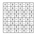
도 2a 및 도 2b는 본 발명의 일 실시예에 따른 수직 2도트 인버젼 방식을 나타낸 도면.2A and 2B illustrate a vertical two-dot inversion scheme according to an embodiment of the present invention.
도 3은 본 발명의 일 실시예에 따른 액정표시장치의 차단회로 및 차단제어회로를 도시한 도면,3 is a diagram illustrating a blocking circuit and a blocking control circuit of a liquid crystal display according to an exemplary embodiment of the present invention;
도 4는 본 발명의 일 실시예에 따른 수직 2도트 인버젼 방식으로 구동하는 액정표시장치의 파형도.4 is a waveform diagram of a liquid crystal display device driven in a vertical 2-dot inversion method according to an embodiment of the present invention.
주요부분에 대한 부호의 설명>Explanation of symbols for main part>
110 : 액정표시패널 130 : 타이밍 컨트롤러110: liquid crystal display panel 130: timing controller
150 : 데이터 드라이버 151 : 차단회로150: data driver 151: blocking circuit
170 : 게이트 드라이버 200 : 차단제어회로170: gate driver 200: cutoff control circuit
211 : 지연기 210 : 제 1 논리 게이트211: delay 210: first logic gate
230 : 제 2 논리 게이트230: second logic gate
본 발명은 액정표시장치에 관한 것으로, 특히 화질저하를 개선할 수 있는 액정표시장치 및 그 구동방법에 관한 것이다.BACKGROUND OF THE
액정표시장치는 비디오 신호에 따라 액정 셀들의 광투과율을 조절하여 화상을 표시하게 된다. 엑티브 매트릭스(Active Matrix) 타입의 액정표시장치는 액정 셀마다 스위칭 소자가 형성되어 동영상을 표시하기에 유리하다. 스위칭 소자로는 주로 박막 트랜지스터(TFT : Thin Film Transistor)가 이용되고 있다.The LCD displays an image by adjusting light transmittance of liquid crystal cells according to a video signal. In an active matrix type liquid crystal display, switching elements are formed in each liquid crystal cell, which is advantageous for displaying moving images. As a switching device, a thin film transistor (TFT) is mainly used.
액정표시장치는 액정표시패널의 액정 셀을 구동하기 위하여 프레임 인버젼 방식(Frame Inversion Method), 라인 인버젼 방식(Line Inversion Method), 컬럼 인버젼 방식(Column Inversion Method) 및 도트 인버젼 방식(Dot Inversion Method)과 같은 인버젼 구동방법이 사용된다.In order to drive a liquid crystal cell of a liquid crystal display panel, a liquid crystal display device uses a frame inversion method, a line inversion method, a column inversion method, and a dot inversion method. Inversion driving methods such as Inversion Method are used.
프레임 인버젼 방식의 액정표시장치는 프레임이 변경될 때마다 액정표시패널에 입력되는 비디오 신호의 극성이 반전된다. 그러나, 프레임 인버젼 방식은 프레임 단위로 플리커가 발생하는 문제점이 있다.In the frame inversion type liquid crystal display device, the polarity of the video signal input to the liquid crystal display panel is reversed whenever the frame is changed. However, the frame inversion method has a problem in that flicker occurs in units of frames.
라인 인버젼 방식의 액정표시장치는 액정표시패널의 게이트 라인 및 프레임마다 비디오 신호의 극성이 반전된다. 그러나, 라인 인버젼 방식은 수평방향 화소들 간의 크로스토크가 존재함에 따라 수직라인들 간에 줄무늬 패턴과 같은 플리커가 발행하는 문제점이 있다.In the line inversion type liquid crystal display, the polarity of the video signal is inverted for each gate line and frame of the liquid crystal display panel. However, the line inversion scheme has a problem in that flicker such as a stripe pattern is generated between vertical lines due to the presence of crosstalk between pixels in the horizontal direction.
컬럼 인버젼 방식의 액정표시장치는 액정표시패널 상의 데이터 라인 및 프레 임마다 비디오 신호의 극성이 반전된다. 그러나, 컬럼 인버젼 방식은 수직방향 화소들 간에 크로스토크가 존재함에 따라 수직라인들 간에 줄무늬 패턴과 같은 플리커가 발생하는 문제점이 있다.In the column inversion type liquid crystal display, polarities of video signals are reversed for each data line and frame on the liquid crystal display panel. However, the column inversion scheme has a problem in that flicker, such as a stripe pattern, occurs between vertical lines as crosstalk exists between vertical pixels.
도트 인버젼 방식 중 1도트 인버젼 방식은 액정 셀들 각각에 수평 및 수직 방향으로 인접하는 액정 셀들 모두 상반된 극성의 비디오 신호가 공급되게 하고, 프레임마다 그 비디오 신호의 극성이 반전된다.One dot inversion method of the dot inversion method allows the liquid crystal cells adjacent to each other in the horizontal and vertical directions to be supplied with a video signal of opposite polarity to each of the liquid crystal cells, and the polarity of the video signal is inverted for each frame.
도트 인버젼 방식 중 2도트 인버젼 방식은 2 라인 단위로 수평 및 수직방향으로 인접하는 액정 셀들 모두와 상반된 극성의 비디오 신호가 공급되게 하고, 프레임마다 그 비디오 신호의 극성이 반전된다. 2도트 인버젼 방식은 수평방향으로 인접한 2개의 액정 셀을 기준으로 동일한 극성을 가지고, 수평방항으로 상기 2개의 액정 셀과 인접한 2개의 액정 셀은 상반된 극성을 가진다.The two-dot inversion method of the dot inversion method allows a video signal having a polarity opposite to that of all adjacent liquid crystal cells in a horizontal and vertical direction in two line units, and the polarity of the video signal is inverted every frame. The two-dot inversion method has the same polarity with respect to two liquid crystal cells adjacent in the horizontal direction, and two liquid crystal cells adjacent to the two liquid crystal cells in the horizontal direction have opposite polarities.
이상에서 설명한 구동방법 중에 2도트 인버젼 방식은 프레임 간에 발생되는 플리커가 서로 상쇄되게 함으로써, 다른 인버젼 방식들에 비하여 뛰어난 화질의 화상을 제공한다.In the above-described driving method, the two-dot inversion method allows flickers generated between frames to cancel each other, thereby providing an image having excellent image quality compared to other inversion methods.
이상에서 설명한 구동방법 중에 2도트 인버젼 방식은 수평방향으로 2개의 액정 셀마다 극성이 반전되는 수평 2도트 인버젼 방식과, 수직방향으로 2개의 액정 셀마다 극성이 반전되는 수직 2도트 인버젼 방식을 포함한다.Among the driving methods described above, the two-dot inversion method includes a horizontal two-dot inversion method in which polarities are inverted in every two liquid crystal cells in a horizontal direction, and a vertical two-dot inversion method in which polarities are inverted in every two liquid crystal cells in a vertical direction. It includes.
상기 수직 2도트 인버젼 방식에 있어서, 수직방향으로 인접한 액정 셀들은 동일한 극성의 화소 전압을 순차적으로 연이어 충전하기 때문에 차징되는 전압의 불균형이 발생한다. 실제로 정극성(또는 부극성)의 데이터 전압을 먼저 충전하는 제 1 액정 셀 보다 상기 제 1 액정 셀과 인접한 다음 라인의 제 2 액정 셀은 긴 시간동안 정극성(또는 부극성)의 데이터 전압을 충전한다.In the vertical two-dot inversion scheme, since the liquid crystal cells adjacent in the vertical direction sequentially charge pixel voltages of the same polarity sequentially, an unbalanced voltage is generated. In fact, the second liquid crystal cell adjacent to the first liquid crystal cell rather than the first liquid crystal cell which first charges the positive (or negative) data voltage charges the positive (or negative) data voltage for a long time. do.
예를 들어 동일한 전압레벨의 화소 데이터 전압을 수직방향으로 인접한 두개의 액정 셀들이 순차적으로 충전하는 경우, 제 2 액정 셀에 충전된 전압은 제 1 액정 셀에 충전된 전압보다 높게 된다. 이로 인하여 화상에는 줄무늬가 나타나게 됨은 물론 화질이 저하될 수밖에 없다.For example, when two liquid crystal cells adjacent in the vertical direction sequentially charge pixel data voltages having the same voltage level, the voltage charged in the second liquid crystal cell becomes higher than the voltage charged in the first liquid crystal cell. As a result, streaks appear in the image, as well as deterioration in image quality.
본 발명은 화질 저하를 방지하기에 적합한 액정표시장치 및 그 구동방법을 제공함에 그 목적이 있다.SUMMARY OF THE INVENTION An object of the present invention is to provide a liquid crystal display and a driving method thereof suitable for preventing deterioration of image quality.
상기한 목적을 달성하기 위한 본 발명의 일 실시예에 따른 액정표시장치는,Liquid crystal display device according to an embodiment of the present invention for achieving the above object,
액정표시패널;A liquid crystal display panel;
상기 액정표시패널의 액정 셀들에 공급되는 화소 데이터 전압의 극성이 수직방향으로 적어도 두개의 액정 셀마다 정극성 및 부극성으로 교번되게 하는 데이터 드라이버;A data driver for causing the polarity of the pixel data voltages supplied to the liquid crystal cells of the liquid crystal display panel to be alternately positive and negative for at least two liquid crystal cells in a vertical direction;
상기 데이터 드라이버로부터 출력되는 상기 화소 데이터 전압을 선택적으로 차단시키는 차단회로; 및A blocking circuit for selectively blocking the pixel data voltage output from the data driver; And
서로 인접할 뿐만 아니라 동일한 극성을 가지는 액정 셀들 간에 상기 화소 데이터 전압의 충전되는 시간이 동일하도록 상기 차단회로를 제어하는 차단제어회로를 포함하여 이루어진다.And a blocking control circuit for controlling the blocking circuit so that the charging time of the pixel data voltage is the same between the liquid crystal cells that are adjacent to each other and have the same polarity.
또한, 본 발명에 따른 액정표시장치의 구동방법은,In addition, the driving method of the liquid crystal display device according to the present invention,
액정표시패널에서 수직방향으로 적어도 두개 이상의 액정 셀마다 정극성 및 부극성의 화소 데이터 전압을 교번적으로 공급하는 단계;Alternately supplying positive and negative pixel data voltages to at least two liquid crystal cells in a vertical direction in a liquid crystal display panel;
상기 액정표시패널의 수직방향에서 동일한 극성을 가지는 액정 셀들의 충전시간 사이에서 일정기간 차단구간을 설정하는 단계; 및Setting a blocking period for a predetermined period between charging times of liquid crystal cells having the same polarity in the vertical direction of the liquid crystal display panel; And
상기 설정된 차단구간 동안 상기 액정표시패널의 데이터 라인들에 공급될 화소 데이터 전압을 차단하는 단계를 포함하여 이루어진다.And blocking a pixel data voltage to be supplied to data lines of the liquid crystal display panel during the set blocking period.
이하, 첨부한 도면을 참조하여 본 발명을 상세히 설명하도록 한다.Hereinafter, the present invention will be described in detail with reference to the accompanying drawings.
도 1은 본 발명의 일 실시예에 따른 액정표시장치를 개략적으로 도시한 도면이고, 도 2a 및 도 2b는 본 발명의 일 실시예에 따른 수직 2도트 인버젼 방식을 나타낸 도면이다.1 is a view schematically showing a liquid crystal display device according to an embodiment of the present invention, Figures 2a and 2b is a view showing a vertical two-dot inversion method according to an embodiment of the present invention.
도 1에 도시된 바와 같이, 본 발명의 일 실시예에 따른 액정표시장치는 데이터 라인들(D1 내지 Dm)과 게이트 라인들(G1 내지 Gn)이 교차되며 그 교차부에 액정 셀(Clc)을 구동하기 위한 TFT가 형성된 액정표시패널(110)과, 상기 액정표시패널(110)의 데이터 라인들(D1 내지 Dm)에 화소 데이터 전압을 공급하기 위한 데이터 드라이버(150)와, 상기 액정표시패널(110)의 게이트 라인들(G1 내지 Gn)에 스캔펄스를 공급하기 위한 게이트 드라이버(170)를 포함한다.As shown in FIG. 1, in the liquid crystal display according to the exemplary embodiment, the data lines D1 to Dm and the gate lines G1 to Gn cross each other, and the liquid crystal cell Clc is disposed at an intersection thereof. A liquid
본 발명의 액정표시장치는 상기 데이터 드라이버(150) 및 게이트 드라이버(170)를 제어하기 위한 타이밍 컨트롤러(130)와, 서로 인접한 액정 셀 중에 같은 극성을 가지는 액정 셀들 간의 차징 전압의 불균형을 개선하기 위한 차단제어회로(200)와, 상기 차단제어회로(200)로부터 입력되는 제어신호(CS)에 응답하여 상기 화소 데이터 전압을 상기 데이터 라인들(D1 내지 Dm)에 차단하는 차단회로(151)를 더 구비한다.The liquid crystal display of the present invention is to improve the imbalance of charging voltage between the
액정표시패널(110)의 데이터 라인들(D1 내지 Dm)과 게이트 라인들(G1 내지 Gn)의 교차부에 형성된 TFT는 게이트 라인들(G1 내지 Gn)으로부터의 스캔펄스에 응답하여 데이트 라인들(D1 내지 Dm) 상의 화소 데이터 전압을 액정 셀(Clc)에 공급하게 된다. 여기서, TFT의 게이트 전극은 게이트 라인들(G1 내지 Gn)에 접속되고, 소스 전극은 데이터 라인들(D1 내지 Dm)에 접속된다. TFT의 드레인 전극은 액정 셀(Clc)의 화소 전극(미도시)에 접속된다. 상기 화소 전극과 대향하는 공통 전극(미도시)에는 공통전압(Vcom)이 공급된다.The TFTs formed at the intersections of the data lines D1 to Dm and the gate lines G1 to Gn of the liquid
액정표시패널(110)의 각 액정 셀(Clc)에는 액정 셀(Clc)에 충전된 전압을 일정하게 유지시키기 위한 스토리지 캐패시터(Cst)가 형성된다.In each liquid crystal cell Clc of the liquid
데이터 드라이버(150)는 일정한 채널 수를 가지는 다수의 데이터 집적회로를 포함한다.The
데이터 집적회로는 클럭을 샘플링하기 위한 쉬프트 레지스터, 데이터를 일시저장하기 위한 레지스터, 쉬프트 레지스터로부터의 클럭신호에 응답하여 데이터를 1 라인분씩 저장하고 저장된 1 라인분의 데이터를 동시에 출력하기 위한 래치, 래 치로부터의 디지털 데이터 값들을 아날로그 신호 형태의 화소 데이터 전압들로 변환하는 디지털-아날로그 변환기 등으로 구성된다.The data integrated circuit includes a shift register for sampling a clock, a register for temporarily storing data, a latch for storing one line of data in response to a clock signal from the shift register, and simultaneously outputting one line of stored data. A digital-to-analog converter or the like for converting digital data values from the data into pixel data voltages in the form of analog signals.
데이터 드라이버(150)는 극성신호(POL)에 응답하여 화소 데이터 전압들의 극성이 수평방향으로 적어도 하나 이상의 액정샐마다 정극성 및 부극성으로 교번되게 한다. 또한, 데이터 드라이버(150)는 극성신호(POL)에 응답하여 화소 데이터 전압들의 극성이 수직방향으로 적어도 두개 이상의 액정샐마다 정극성 및 부극성으로 교번되게 한다.The
본 발명은 도 2a 참조하여 수평방향으로 하나의 액정 셀마다 정극성 및 부극성이 교번되고, 수직방향으로 두개의 액정 셀마다 정극성 및 부극성이 교번된다. 또한, 본 발명은 도 2b를 참조하여 프레임마다 모든 액정 셀들이 반전되는 수직 2도트 인버젼 방식을 일 실시예로 설명한다.The present invention alternates the positive and negative polarities for every one liquid crystal cell in the horizontal direction with reference to FIG. 2A, and the positive and negative polarities are alternated for each of the two liquid crystal cells in the vertical direction. In addition, the present invention describes a vertical two-dot inversion scheme in which all liquid crystal cells are inverted per frame with reference to FIG. 2B.
이와 같은 데이터 집적회로는 타이밍 컨트롤러(130)의 제어에 의해 데이터 라인들(D1 내지 Dm)로 화소 데이터 전압을 공급한다.Such a data integrated circuit supplies the pixel data voltage to the data lines D1 to Dm under the control of the
게이트 드라이버(170)는 스캔펄스를 순차적으로 발생하는 쉬프트 레지스터와, 스캔펄스의 전압을 액정 셀(Clc)의 구동에 적합한 레벨로 쉬프트시키기 위한 레벨 쉬프터 등으로 구성된다.The
게이트 드라이버(170)는 타이밍 컨트롤러(130)의 제어에 의해 게이트 라인들(G1 내지 Gn)에 순차적으로 스캔펄스를 공급한다.The
타이밍 컨트롤러(130)는 수직/수평 동기신호(Vsync, Hsync), 클럭(CLK) 및 데이터 이네이블 신호(DE) 등을 이용하여 상기 데이터 드라이버(150)를 제어하기 위한 데이터 제어신호(DDC)와, 상기 게이트 드라이버(170)를 제어하기 위한 게이트 제어신호(GDC)를 생성한다.The
데이터 제어신호(DDC)는 소스 스타트 펄스(SSP), 소스 쉬프트 클럭(SSC), 소스 출력제어신호(SOE) 및 극성신호(POL) 등을 포함한다.The data control signal DDC includes a source start pulse SSP, a source shift clock SSC, a source output control signal SOE, a polarity signal POL, and the like.
게이트 제어신호(GDC)는 게이트 스타트 펄스(GSP), 게이트 쉬프트 클럭(GSC), 게이트 출력신호(GOE) 등을 포함한다.The gate control signal GDC includes a gate start pulse GSP, a gate shift clock GSC, a gate output signal GOE, and the like.
차단회로(151)는 차단제어회로(200)로부터의 제어신호(CS)에 응답하여, 데이터 라인들(D1 내지 Dm) 간의 전하를 차단시키거나 데이터 드라이버(150)로부터 m개의 화소 데이터 전압을 대응하는 데이터 라인들(D1 내지 Dm)쪽으로 전송한다. 이를 상세히 설명하면, 차단제어신호(CS)가 특정 논리(예를 들면, 고전위 전압, 즉 하이논리)를 가지면, 차단회로(151)는 데이터 라인들(D1 내지 Dm)을 서로 연결시켜 모든 데이터 라인들(D1 내지 Dm)에 해당하는 화소 데이터 전압을 공급한다. 반대로 차단제어신호(CS)가 특정 논리(예를 들면, 저전위 전압, 즉 로우논리)를 가지면, 차단회로(151)는 데이터 라인들(D1 내지 Dm)과 연결을 차단한다.The blocking
차단제어회로(200)에는 상기 타이밍 컨트롤러(130)로부터의 소스 출력제어신호(SOE) 및 극성신호(POL)가 입력된다.The source control signal SOE and the polarity signal POL from the
차단제어회로(200)는 수직 2도트 인버젼 방식으로 구동되는 액정표시패널(110)에서 서로 인접하고, 동일한 극성을 가지는 액정 셀들 간의 차징 전압의 불균형을 개선하는 역할을 한다.The blocking
차단제어회로(200)는 타이밍 컨트롤러(130)로부터 입력된 소스 출력제어신 호(SOE) 및 극성신호(POL)를 이용하여 수직방향으로 동일한 극성을 가지는 액정 셀들 사이의 전압이 유기되도록 한다.The blocking
본 발명에서는 수직 2도트 인버젼 방식의 액정표시장치를 한정하여 설명하고 있지만, 이에 한정하지 않고, 수직방향으로 두개 이상의 액정 셀마다 정극성 및 부극성의 화소 데이터 전압이 교번되는 인버젼 방식의 액정표시장치는 모두 적용될 수 있다.In the present invention, a liquid crystal display device having a vertical two-dot inversion method is limited and described. However, the present invention is not limited thereto, and an inversion liquid crystal in which positive and negative pixel data voltages are alternated for two or more liquid crystal cells in a vertical direction. Both display devices can be applied.
이상에서 설명한 본 발명의 일 실시예에 따른 액정표시장치는 수직 2도트 인버젼 방식에 있어서, 수직방향으로 동일한 극성을 가지는 화소 데이터 전압 사이에서 차지 쉐어 동작이 일어난다. 따라서, 본 발명은 수직방향으로 동일한 극성을 가지는 액정 셀 간의 차징되는 전압의 불균형을 개선할 수 있다.In the liquid crystal display according to the exemplary embodiment described above, in the vertical 2-dot inversion scheme, the charge share operation occurs between pixel data voltages having the same polarity in the vertical direction. Therefore, the present invention can improve the imbalance of the voltage charged between the liquid crystal cells having the same polarity in the vertical direction.
도 3은 본 발명의 일 실시예에 따른 액정표시장치의 차단회로 및 차단제어회로를 도시한 도면이다.3 is a diagram illustrating a blocking circuit and a blocking control circuit of a liquid crystal display according to an exemplary embodiment of the present invention.
도 3에 도시된 바와 같이, 본 발명의 일 실시예에 따른 액정표시장치는 차단 회로(151)와, 차단제어회로(200)를 포함한다.As shown in FIG. 3, the liquid crystal display according to the exemplary embodiment of the present invention includes a
차단회로(151)는 차단제어신호(CS)에 응답하여 데이터 라인들(D1 내지 Dm)의 전하를 차안시키거나 데이터 라인들(D1 내지 Dm)에 대응되는 m개의 화소 데이터 전압을 공급한다. 여기서 상기 화소 데이터 전압은 도시되지 않은 데이터 직접회로로부터 입력된다.The blocking
상기 데이터 직접회로는 상세히 도시하지는 않았지만, 데이터 라인(D1 내지 Dm)에 종속적으로 접속된 쉬프트 레지스터와, 래치, 디지털-아날로그 변환기(DAC: disital to analog convertor)를 더 포함한다.Although not shown in detail, the data integrated circuit further includes a shift register connected to data lines D1 to Dm, and a latch and a digital-to-analog converter (DAC).
쉬프트 레지스터는 타이밍 컨트롤러로부터 소스 스타트 펄스(SSP)를 소스 쉬프트 클럭신호(SSC)에 따라 쉬프트시켜 샘플링 신호(SCLK)를 발생한다. 또한, 쉬프트 레지스터는 소스 스타트 펄스(SSP)를 쉬프트시켜 다음 단의 쉬프트 레지스터에 캐리신호(CAR)를 전달한다.The shift register shifts the source start pulse SSP from the timing controller according to the source shift clock signal SSC to generate the sampling signal SCLK. In addition, the shift register shifts the source start pulse SSP to transfer the carry signal CAR to the next stage shift register.
래치는 쉬프트 레지스터로부터 입력되는 샘플링신호에 따라 디지털 데이터(R,G,B)를 샘플링하여 저장하고, 타이밍 컨트롤러로부터의 소스 출력제어신호(SOE)에 응답하여 1수평 라인분의 데이터를 동시에 출력한다.The latch samples and stores the digital data R, G, and B according to the sampling signal input from the shift register, and simultaneously outputs one horizontal line of data in response to the source output control signal SOE from the timing controller. .
디지털-아날로그 변환기(DAC)는 래치로부터의 디지털 데이터(R,G,B)를 감마전압 세트를 이용하여 아날로그 신호 형태의 화소 데이터 전압으로 변환한다. 여기서, 디지털-아날로그 변환기(DAC)는 극성신호(POL)에 응답하여 컬럼 인버젼, 프레임 인버젼, 1도트 인버젼, 2도트 인버젼 및 3도트 인버젼 등의 인버젼 방식에 따라 데이터의 극성을 변화한다. 본 발명에서는 수직 2도트 인버젼 방식을 일 예로 설명하고 있다.The digital-to-analog converter DAC converts the digital data R, G, and B from the latch into pixel data voltages in the form of analog signals using a gamma voltage set. Herein, the digital-to-analog converter DAC responds to the polarity signal POL according to the inversion scheme such as column inversion, frame inversion, 1-dot inversion, 2-dot inversion, and 3-dot inversion. To change. In the present invention, the vertical 2-dot inversion method is described as an example.
차단회로(151)는 데이터 라인(D1 내지 Dm) 각각에 연결된 다수의 스위치들(SW1 내지 SWm)을 포함한다.The blocking
차단제어회로(200)는 상기 차단회로(151)로부터 데이터 라인(D1 내지 Dm)으로 출력되는 화소 데이터 전압(R.G.B) 중에 수직방향으로 서로 인접할 뿐만 아니라 동일한 극성을 가지는 제 1 라인의 액정 셀들의 다음 라인, 즉 제 2 라인의 액정 셀들의 전하가 일정기간 차단되도록 상기 차단회로(151)를 제어한다.The
차단제어회로(200)는 지연기(211), 배타적 부정 논리합 연산하는 제 1 논리 게이트(XNOR, 210) 및 논리곱 연산하는 제 2 논리 게이트(AND, 230)를 포함한다. The
지연기(211)는 타이밍 컨트롤러로부터 입력되는 극성신호(POL)를 일정기간 지연하여 출력한다.The
제 1 논리 게이트(XNOR, 210)는 상기 지연기(211)의 출력과, 타이밍 컨트롤러로부터 입력되는 극성신호(POL)를 연산한다.The first
제 2 논리 게이트(AND, 230)는 상기 제 1 논리 게이트(XNOR, 210)로부터의 출력과, 타이밍 컨트롤러로부터 입력되는 소스 출력제어신호(SOE)를 연산한다.The second logic gate (AND) 230 calculates an output from the first logic gate (XNOR) 210 and a source output control signal SOE input from a timing controller.
제 2 논리 게이트(AND, 230)로부터 출력되는 제어신호(CS)는 상기 차단회로(151)로부터 출력되는 화소 데이터 전압(R,G,B) 중 수직방향으로 서로 인접하는 액정 셀들 중 후행의 액정 셀들의 전하를 일시적으로 차단시킴으로써, 액정 셀들 간의 차징되는 전압의 불균형을 개선할 수 있다.The control signal CS output from the second logic gates AND and 230 is a subsequent liquid crystal among the liquid crystal cells adjacent to each other in the vertical direction among the pixel data voltages R, G and B output from the blocking
도 4는 본 발명의 일 실시예에 따른 수직 2도트 인버젼 방식으로 구동하는 액정표시장치의 파형도이다.4 is a waveform diagram of a liquid crystal display device driven in a vertical 2-dot inversion method according to an embodiment of the present invention.
도 4에 도시된 바와 같이, 본 발명의 수직 2도트 인버젼 방식으로 구동하는 액정표시장치는 타이밍 컨트롤러로부터 출력되는 극성신호(POL)가 지연기 및 제 1 논리 게이트(XNOR)로 공급된다.As shown in FIG. 4, in the liquid crystal display device driven by the vertical 2-dot inversion method, the polarity signal POL output from the timing controller is supplied to the delay unit and the first logic gate XNOR.
본 발명의 액정표시장치는 수직방향으로 2개의 액정 셀 단위로 극성이 반전될 뿐만 아니라 수평방향으로 인접한 액정 셀들 간에 서로 다른 극성을 가진다. 또한 액정 셀들의 극성은 프레임마다 반전된다.The liquid crystal display of the present invention not only has polarity reversed in units of two liquid crystal cells in the vertical direction but also has different polarities between adjacent liquid crystal cells in the horizontal direction. In addition, the polarities of the liquid crystal cells are inverted frame by frame.
상기 극성신호(POL)가 입력된 지연기는 극성신호(POL)를 일정 시간 지연하여 제 1 논리 게이트(XNOR)로 공급한다.The delay unit, to which the polarity signal POL is input, delays the polarity signal POL for a predetermined time and supplies it to the first logic gate XNOR.
지연기는 원래(지연되지 않은)의 극성신호(POL)와 중첩되지 않은 하나의 소스 출력제어신호(SOE)의 하이펄스(H1)와 중첩될 수 있도록 극성신호(POL)를 지연시킨다.The delay unit delays the polarity signal POL so that it can overlap with the high pulse H1 of one source output control signal SOE not overlapping with the original (non-delayed) polarity signal POL.
제 1 논리 게이트(XNOR)는 상기 지연기로부터 출력되는 지연된 극성신호(DPOL)와 타이밍 컨트롤러로부터 입력되는 지연되지 않은 극성신호(POL)를 연산한다. 이때, 제 1 논리 게이트(XNOR)에서 출력되는 펄스는 입력된 소스 출력제어신호(SOE)의 하이펄스와 교번적으로 중첩되도록 출력된다.The first logic gate XNOR calculates the delayed polarity signal DPOL output from the delayer and the non-delayed polarity signal POL input from the timing controller. At this time, the pulse output from the first logic gate XNOR is output to alternately overlap with the high pulse of the input source output control signal SOE.
제 2 논리 게이트(AND)는 상기 제 1 논리 게이트(XNOR)로부터의 출력펄스와 소스 출력제어신호(SOE)를 연산한다. 이때, 제 2 논리 게이트(AND)에서 출력되는 펄스(CS)는 2 수평주기의 주기를 가지게 된다. 또한, 제 2 논리 게이트(AND)에서 출력되는 펄스(CS)는 상기 소스 출력제어신호(SOE)의 하이펄스와 교번적으로 중첩될 뿐만 아니라 상기 극성신호(POL)와 동일한 펄스 폭을 가진다.The second logic gate AND calculates an output pulse from the first logic gate XNOR and a source output control signal SOE. At this time, the pulse CS output from the second logic gate AND has a period of two horizontal periods. In addition, the pulse CS output from the second logic gate AND not only overlaps with the high pulse of the source output control signal SOE, but also has the same pulse width as the polarity signal POL.
제 2 논리 게이트(AND)로부터 출력되는 제어신호(CS)의 하이구간에서는 동일한 극성을 가지는 액정 셀들 사이의 구간과 중첩된다. 즉, 데이터 라인에는 동일한 극성을 가지는 화소 데이터 전압 사이의 전압이 유기된다.The high section of the control signal CS output from the second logic gate AND overlaps the section between the liquid crystal cells having the same polarity. That is, voltages between pixel data voltages having the same polarity are induced in the data lines.
제어신호(CS)의 하이구간에서는 1 라인 분의 화소 데이터 전압 중에 수직방향으로 동일한 극성을 가지며 서로 인접한 액정 셀 간의 차징되는 전압 편차를 줄이기 위해 후행 액정 셀들의 전압이 일시적으로 유기된다. 즉, 후행의 액정 셀들은 일정기간 화소 데이터 전압이 충전되지 않는 차단구간을 가진다.In the high section of the control signal CS, voltages of the following liquid crystal cells are temporarily induced to reduce voltage variations between the liquid crystal cells having the same polarity in the vertical direction among the pixel data voltages for one line and adjacent to each other. That is, the subsequent liquid crystal cells have a blocking period in which the pixel data voltage is not charged for a predetermined period of time.
제 2 논리 게이트(AND)로부터 출력되는 제어신호(CS)의 로우구간에서는 데이터 라인으로 화소 데이터 전압의 전압레벨은 변동 없이 출력된다.In the low section of the control signal CS output from the second logic gate AND, the voltage level of the pixel data voltage is output to the data line without change.
이상에서 설명한 본 발명의 일 실시예에 따른 액정표시장치는 수직 2도트 인버젼 방식에 있어서, 수직방향으로 동일한 극성을 가지는 화소 데이터 전압 사이에서 차지 쉐어 동작이 일어난다. 따라서, 본 발명에서는 동일한 극성을 가지는 액정 셀 간의 차징되는 전압의 불균형을 개선할 수 있다.In the liquid crystal display according to the exemplary embodiment described above, in the vertical 2-dot inversion scheme, the charge share operation occurs between pixel data voltages having the same polarity in the vertical direction. Therefore, in the present invention, the imbalance of the voltage charged between the liquid crystal cells having the same polarity can be improved.
즉, 본 발명에서는 동일한 극성을 가지는 액정 셀 간의 차징되는 전압의 불균형을 개선함으로써, 줄무늬 현상 등의 화질 저하를 개선할 수 있다.That is, in the present invention, by reducing the imbalance of the voltage charged between the liquid crystal cells having the same polarity, it is possible to improve the deterioration of image quality such as striation phenomenon.
이상에서 살펴본 바와 같이, 본 발명은 수직 2도트 인버젼 방식으로 구동되는 액정표시장치에 있어서, 수직방향으로 서로 인접함과 동시에 동일한 극성을 가지는 액정 셀들 중 후행 액정 셀들의 전하를 차단시킨 후 화소 데이터 전압을 공급함으로써, 전행 액정 셀들 및 후행 액정 셀들 간에 화소 데이터 전압의 차징되는 시간을 동일하게 하여 줄무늬 현상 등의 화질 저하를 개선할 수 있는 효과가 있다.As described above, the present invention is a liquid crystal display device driven in a vertical 2-dot inversion method, the pixel data after blocking the charge of the following liquid crystal cells of the liquid crystal cells adjacent to each other in the vertical direction and at the same time have the same polarity By supplying the voltage, the charging time of the pixel data voltage is made the same between the preceding liquid crystal cells and the subsequent liquid crystal cells, thereby improving the image quality deterioration such as a streak phenomenon.
이상 설명한 내용을 통해 통상의 지식을 가진 자라면 본 발명의 기술사상을 일탈하지 아니하는 범위에서 다양한 변경 및 수정이 가능할 것이다. 따라서, 본 발명의 기술적 범위는 명세서의 상세한 설명에 기재된 내용으로 한정되는 것이 아니라 특허 청구의 범위에 의해 정하여져야만 할 것이다.Those skilled in the art through the above description will be capable of various changes and modifications without departing from the spirit of the present invention. Therefore, the technical scope of the present invention should not be limited to the contents described in the detailed description of the specification but should be defined by the claims.
Claims (7)
Priority Applications (1)
| Application Number | Priority Date | Filing Date | Title |
|---|---|---|---|
| KR1020070042498A KR20080097530A (en) | 2007-05-02 | 2007-05-02 | LCD and its driving method |
Applications Claiming Priority (1)
| Application Number | Priority Date | Filing Date | Title |
|---|---|---|---|
| KR1020070042498A KR20080097530A (en) | 2007-05-02 | 2007-05-02 | LCD and its driving method |
Publications (1)
| Publication Number | Publication Date |
|---|---|
| KR20080097530A true KR20080097530A (en) | 2008-11-06 |
Family
ID=40285313
Family Applications (1)
| Application Number | Title | Priority Date | Filing Date |
|---|---|---|---|
| KR1020070042498A Withdrawn KR20080097530A (en) | 2007-05-02 | 2007-05-02 | LCD and its driving method |
Country Status (1)
| Country | Link |
|---|---|
| KR (1) | KR20080097530A (en) |
Cited By (2)
| Publication number | Priority date | Publication date | Assignee | Title |
|---|---|---|---|---|
| US9691341B2 (en) | 2014-09-29 | 2017-06-27 | Samsung Display Co., Ltd. | Data driver and display apparatus including the same |
| KR20180021967A (en) * | 2016-08-22 | 2018-03-06 | 엘지디스플레이 주식회사 | Controller, display device, and the method for driving the display device |
-
2007
- 2007-05-02 KR KR1020070042498A patent/KR20080097530A/en not_active Withdrawn
Cited By (2)
| Publication number | Priority date | Publication date | Assignee | Title |
|---|---|---|---|---|
| US9691341B2 (en) | 2014-09-29 | 2017-06-27 | Samsung Display Co., Ltd. | Data driver and display apparatus including the same |
| KR20180021967A (en) * | 2016-08-22 | 2018-03-06 | 엘지디스플레이 주식회사 | Controller, display device, and the method for driving the display device |
Similar Documents
| Publication | Publication Date | Title |
|---|---|---|
| KR102081135B1 (en) | Display Device Capable Of Driving In Low-Speed | |
| KR101245944B1 (en) | Liquid crystal panel, liquid crystal display device having same and driving method thereof | |
| KR102081131B1 (en) | Display Device Being Capable Of Driving In Low-Speed | |
| KR102268520B1 (en) | Display device and method for driving the same | |
| KR101252854B1 (en) | Liquid crystal panel, data driver, liquid crystal display device having the same and driving method thereof | |
| KR20120116615A (en) | Liquid crystal display device and method for driving the same | |
| JP4566975B2 (en) | Liquid crystal display device and driving method thereof | |
| KR20070109296A (en) | LCD and its driving method | |
| KR101278001B1 (en) | Driving liquid crystal display and apparatus for driving the same | |
| KR20090070253A (en) | LCD and its driving method | |
| KR20080097530A (en) | LCD and its driving method | |
| KR100477598B1 (en) | Apparatus and Method for Driving Liquid Crystal Display of 2 Dot Inversion Type | |
| KR102349502B1 (en) | Liquid Crystal Display Device and Driving Method thereof | |
| KR101174783B1 (en) | Apparatus and method for driving of liquid crystal display device | |
| KR100831284B1 (en) | Driving Method of LCD | |
| KR101376655B1 (en) | Common voltage supply circuit of liquid crystal display device | |
| KR102480834B1 (en) | Display Device Being Capable Of Driving In Low-Speed | |
| KR101220206B1 (en) | Driving device of LCD and Driving method the same | |
| KR20070069797A (en) | LCD and its driving method | |
| KR20080026278A (en) | Data driving device and driving method thereof | |
| KR100680057B1 (en) | Precharging method and apparatus of liquid crystal display | |
| KR20080099410A (en) | LCD and its driving method | |
| KR20070079103A (en) | LCD and its driving method | |
| KR20070030344A (en) | LCD and its driving method | |
| KR20100064567A (en) | Liquid crystal display device |
Legal Events
| Date | Code | Title | Description |
|---|---|---|---|
| PA0109 | Patent application |
Patent event code: PA01091R01D Comment text: Patent Application Patent event date: 20070502 |
|
| PG1501 | Laying open of application | ||
| PC1203 | Withdrawal of no request for examination | ||
| WITN | Application deemed withdrawn, e.g. because no request for examination was filed or no examination fee was paid |