KR101151456B1 - Adaptive electropolishing using thickness measurements and removal of barrier and sacrificial layers - Google Patents
Adaptive electropolishing using thickness measurements and removal of barrier and sacrificial layers Download PDFInfo
- Publication number
- KR101151456B1 KR101151456B1 KR1020057001191A KR20057001191A KR101151456B1 KR 101151456 B1 KR101151456 B1 KR 101151456B1 KR 1020057001191 A KR1020057001191 A KR 1020057001191A KR 20057001191 A KR20057001191 A KR 20057001191A KR 101151456 B1 KR101151456 B1 KR 101151456B1
- Authority
- KR
- South Korea
- Prior art keywords
- layer
- metal layer
- delete delete
- recessed region
- polishing
- Prior art date
- Legal status (The legal status is an assumption and is not a legal conclusion. Google has not performed a legal analysis and makes no representation as to the accuracy of the status listed.)
- Expired - Lifetime
Links
Images


Classifications
-
- H—ELECTRICITY
- H10—SEMICONDUCTOR DEVICES; ELECTRIC SOLID-STATE DEVICES NOT OTHERWISE PROVIDED FOR
- H10P—GENERIC PROCESSES OR APPARATUS FOR THE MANUFACTURE OR TREATMENT OF DEVICES COVERED BY CLASS H10
- H10P52/00—Grinding, lapping or polishing of wafers, substrates or parts of devices
-
- H—ELECTRICITY
- H10—SEMICONDUCTOR DEVICES; ELECTRIC SOLID-STATE DEVICES NOT OTHERWISE PROVIDED FOR
- H10P—GENERIC PROCESSES OR APPARATUS FOR THE MANUFACTURE OR TREATMENT OF DEVICES COVERED BY CLASS H10
- H10P50/00—Etching of wafers, substrates or parts of devices
- H10P50/20—Dry etching; Plasma etching; Reactive-ion etching
- H10P50/26—Dry etching; Plasma etching; Reactive-ion etching of conductive or resistive materials
- H10P50/264—Dry etching; Plasma etching; Reactive-ion etching of conductive or resistive materials by chemical means
- H10P50/266—Dry etching; Plasma etching; Reactive-ion etching of conductive or resistive materials by chemical means by vapour etching only
- H10P50/269—Dry etching; Plasma etching; Reactive-ion etching of conductive or resistive materials by chemical means by vapour etching only pre- or post-treatments, e.g. anti-corrosion processes
-
- B—PERFORMING OPERATIONS; TRANSPORTING
- B23—MACHINE TOOLS; METAL-WORKING NOT OTHERWISE PROVIDED FOR
- B23H—WORKING OF METAL BY THE ACTION OF A HIGH CONCENTRATION OF ELECTRIC CURRENT ON A WORKPIECE USING AN ELECTRODE WHICH TAKES THE PLACE OF A TOOL; SUCH WORKING COMBINED WITH OTHER FORMS OF WORKING OF METAL
- B23H5/00—Combined machining
- B23H5/06—Electrochemical machining combined with mechanical working, e.g. grinding or honing
- B23H5/08—Electrolytic grinding
-
- C—CHEMISTRY; METALLURGY
- C25—ELECTROLYTIC OR ELECTROPHORETIC PROCESSES; APPARATUS THEREFOR
- C25F—PROCESSES FOR THE ELECTROLYTIC REMOVAL OF MATERIALS FROM OBJECTS; APPARATUS THEREFOR
- C25F3/00—Electrolytic etching or polishing
- C25F3/02—Etching
-
- C—CHEMISTRY; METALLURGY
- C25—ELECTROLYTIC OR ELECTROPHORETIC PROCESSES; APPARATUS THEREFOR
- C25F—PROCESSES FOR THE ELECTROLYTIC REMOVAL OF MATERIALS FROM OBJECTS; APPARATUS THEREFOR
- C25F7/00—Constructional parts, or assemblies thereof, of cells for electrolytic removal of material from objects; Servicing or operating
-
- H—ELECTRICITY
- H10—SEMICONDUCTOR DEVICES; ELECTRIC SOLID-STATE DEVICES NOT OTHERWISE PROVIDED FOR
- H10P—GENERIC PROCESSES OR APPARATUS FOR THE MANUFACTURE OR TREATMENT OF DEVICES COVERED BY CLASS H10
- H10P52/00—Grinding, lapping or polishing of wafers, substrates or parts of devices
- H10P52/20—Electromechanical polishing [EMP]; Electrochemical mechanical polishing [ECMP]
- H10P52/203—Electromechanical polishing [EMP]; Electrochemical mechanical polishing [ECMP] of conductive or resistive materials
-
- H—ELECTRICITY
- H10—SEMICONDUCTOR DEVICES; ELECTRIC SOLID-STATE DEVICES NOT OTHERWISE PROVIDED FOR
- H10W—GENERIC PACKAGES, INTERCONNECTIONS, CONNECTORS OR OTHER CONSTRUCTIONAL DETAILS OF DEVICES COVERED BY CLASS H10
- H10W20/00—Interconnections in chips, wafers or substrates
- H10W20/01—Manufacture or treatment
- H10W20/031—Manufacture or treatment of conductive parts of the interconnections
- H10W20/062—Manufacture or treatment of conductive parts of the interconnections by smoothing of conductive parts, e.g. by planarisation
Landscapes
- Chemical & Material Sciences (AREA)
- Engineering & Computer Science (AREA)
- Chemical Kinetics & Catalysis (AREA)
- Electrochemistry (AREA)
- Organic Chemistry (AREA)
- Metallurgy (AREA)
- Materials Engineering (AREA)
- Mechanical Engineering (AREA)
- Internal Circuitry In Semiconductor Integrated Circuit Devices (AREA)
- Mechanical Treatment Of Semiconductor (AREA)
- Weting (AREA)
- Drying Of Semiconductors (AREA)
- ing And Chemical Polishing (AREA)
Abstract
반도체 웨이퍼상에 형성된 금속층이 적정하게 전해연마된다. 상기 금속층의 일부가 전해연마되며, 여기서 상기 금속층의 부분들은 각각 전해연마된다. 상기 부분을 전해연마하기 전에, 전해연마하고자 하는 금속층의 부분의 두께 측정이 이루어진다. 전해연마될 부분의 양이 두께 측정에 기초하여 조절된다. 반도체 웨이퍼상에 형성된 금속층이 폴리싱되며, 여기서 상기 금속층은 장벽층상에 형성되고, 상기 장벽층은 리세스 영역과 비 리세스 영역을 가진 유전층상에 형성되며, 상기 금속층은 상기 유전층의 리세스 영역과 비 리세스 영역을 덮는다. 상기 비 리세스 영역을 덮고 있는 금속층을 제거하기 위하여 상기 금속층은 폴리싱된다. 상기 리세스 영역내의 금속층은 비 리세스 영역 아래의 높이로 폴리싱되며, 여기서 상기 높이는 장벽층의 두께보다 더 크거나 같다.

The metal layer formed on the semiconductor wafer is appropriately electrolytically polished. A portion of the metal layer is electrolytically polished, wherein portions of the metal layer are each electropolished. Before the electrolytic polishing of the portion, the thickness of the portion of the metal layer to be electrolytically polished is measured. The amount of the portion to be electrolytically polished is adjusted based on the thickness measurement. A metal layer formed on a semiconductor wafer is polished, wherein the metal layer is formed on a barrier layer, the barrier layer is formed on a dielectric layer having a recessed region and a non-recessed region, the metal layer having a recessed region Covering the non-recessed area. The metal layer is polished to remove the metal layer covering the non-recessed region. The metal layer in the recessed region is polished to a height below the non-recessed region, wherein the height is greater than or equal to the thickness of the barrier layer.
Description
본 출원은 "기판상의 금속 필름을 전해연마하는 방법"이란 명칭으로 2002년 7월 22일자에 출원된 미국 가출원 제60/397,941호 및 "장벽층과 희생층의 제거방법"이란 명칭으로 2002년 8월 17일자에 출원된 미국 가출원 제60/403,996호를 우선권 주장하며, 본원은 이들의 내용 전체를 참조하였다. This application is a continuation-in-part of US Provisional Application No. 60 / 397,941, entitled " Method for Electropolishing a Metal Film on a Substrate ", filed July 22,2002, U.S. Provisional Application No. 60 / 403,996, filed May 17, 2006, the entire contents of which are incorporated herein by reference.
본 발명은 기판상에 형성된 금속 필름을 전해연마하는 방법 및 시스템에 관한 것으로, 특히 금속 필름의 두께 측정을 이용하여 반도체 웨이퍼상에 형성된 금속 필름을 적정 전해연마하는 방법 및 시스템에 관한 것이다. 또한, 본 발명은 폴리싱 및 플라즈마 에칭 프로세스에서 장벽층과 희생층을 제거하는 방법 및 시스템에 관한 것이다. The present invention relates to a method and system for electrolytically polishing a metal film formed on a substrate, and more particularly, to a method and system for appropriately electropolishing a metal film formed on a semiconductor wafer using the thickness measurement of the metal film. The present invention also relates to a method and system for removing a barrier layer and a sacrificial layer in a polishing and plasma etching process.
반도체 장치는 트랜지스터 및 인터커넥션 소자(interconnection elements)를 생성하기 위하여 여러가지 프로세싱 단계를 이용하여 반도체 웨이퍼상에 형성 또는 제조된다. 트랜지스터 및/또는 인터커넥션 소자를 형성하기 위하여, 반도체 웨이퍼는 예를 들어 마스킹, 에칭 및 증착 프로세스를 거침으로써, 반도체 장치의 전자 회로를 형성하게 된다. 특히, 다마신 프로세스에서, 인터커넥션을 위한 트렌치 및 비아 역할을 하는 리세스 영역(recessed areas) 패턴을 반도체 웨이퍼의 유전층에 형성하기 위해 다중의 마스킹 및 에칭 단계가 실시될 수 있다. 그 다음, 상기 반도체 웨이퍼상에 금속층을 증착함으로써 트렌치 및 비아와 아울러 반도체 웨이퍼상의 비 리세스 영역(non-recessed areas)에도 금속이 증착되도록 하는 증착 프로세스가 실시될 수 있다. 패턴화된 트렌치 및 비아와 같은 인터커넥션을 절연시키기 위하여, 반도체 웨이퍼의 비 리세스 영역에 증착된 금속층이 제거된다. Semiconductor devices are formed or fabricated on semiconductor wafers using various processing steps to produce transistors and interconnection elements. To form transistors and / or interconnection elements, a semiconductor wafer is subjected to, for example, masking, etching and deposition processes to form electronic circuits of the semiconductor device. In particular, in the damascene process, multiple masking and etching steps can be performed to form recessed areas patterns serving as trenches and vias for interconnection in the dielectric layer of the semiconductor wafer. A deposition process may then be performed to deposit metal on non-recessed areas on the semiconductor wafer, as well as trenches and vias, by depositing a metal layer on the semiconductor wafer. In order to insulate interconnection such as patterned trenches and vias, the metal layer deposited on the non-recessed region of the semiconductor wafer is removed.
그러나, 과도하거나 불충분한 양의 금속층이 제거되면, 트랜지스터 및/또는 인터커넥션 소자는 제대로 작동하지 않게 된다. 예를 들어, 인터커넥션을 형성하는 트렌치로부터 과도한 양의 금속층이 제거되면, 상기 인터커넥션은 전기신호를 적절하게 전송할 수 없게 된다. However, if an excessive or insufficient amount of metal layer is removed, the transistors and / or interconnection elements will not work properly. For example, if an excessive amount of metal layer is removed from the trenches forming the interconnection, the interconnection will not be able to properly transmit electrical signals.
도체의 인터커넥션에서 시간 지연을 줄이기 위한 방법으로서, 낮은 유전상수(저유전율 k)를 가진 유전재료의 사용이 소개되었다. 그러나, 저유전율 재료는 다공성 미세구조를 갖기 때문에, 이들은 다른 유전재료에 비해 기계적 안정성과 열전도성이 낮다. 따라서, 통상적으로, 저유전율 재료는 종래의 다마신 프로세스에서 가해지는 응력과 압력을 견딜 수 없다. As a method for reducing the time delay in conductor interconnection, the use of dielectric materials with low dielectric constants (low dielectric constant k) has been introduced. However, since low dielectric constant materials have a porous microstructure, they have low mechanical stability and low thermal conductivity compared to other dielectric materials. Thus, typically, low dielectric constant materials can not withstand the stresses and pressures exerted in conventional damascene processes.
종래의 다마신 프로세스에서, 금속층 또는 저유전율 재료상에 장벽층이 형성될 수 있다. 통상적으로, 상기 장벽층은 TaN, Ta, Ti 및 TiN과 같이 강하고 화학적으로 불활성인 재료로 형성되기 때문에, CMP과정에서 높은 패드압력을 이용하거나 고압 전해연마를 제외하고, CMP 또는 전해연마를 이용하여 장벽층을 제거하는 것은 어렵다. CMP의 경우, 높은 패드압력은 표면 결함 밀도를 증가시키거나, 저유전율 재료를 갈라지게 할 수도 있다. 전해연마의 경우, 높은 폴리싱 압력은 과도한 양의 금속을 제거할 수 있으며, 이는 라인 저항(line resistance)을 증가시킬 수 있다. 장벽층을 제거하기 위해 종래의 플라즈마 에칭을 사용하는 경우, 비 리세스 영역의 모든 장벽층이 제거되도록 하기 위하여 과에칭(over-etching)이 필요하다. 그러나, 과에칭은 다음 커버층이 증착될 때 공동(voids)을 유발할 수 있다. 금속 원자가 상기 공동으로부터 확산될 수 있으며, 장치의 게이트 영역으로 확산될 수 있고, 이로 인하여 반도체 장치가 제대로 작동하지 않게 될 수 있다. In a conventional damascene process, a barrier layer may be formed on a metal layer or a low dielectric constant material. Typically, since the barrier layer is formed of a strong and chemically inert material such as TaN, Ta, Ti, and TiN, a high pad pressure may be used in the CMP process, or alternatively, using CMP or electrolytic polishing, It is difficult to remove the barrier layer. In the case of CMP, high pad pressures may increase the surface defect density, or may break the low dielectric constant material. In the case of electrolytic polishing, a high polishing pressure can remove an excessive amount of metal, which can increase line resistance. If a conventional plasma etch is used to remove the barrier layer, over-etching is required to remove all barrier layers in the non-recessed region. However, overetching can cause voids when the next cover layer is deposited. Metal atoms may diffuse out of the cavity and diffuse into the gate region of the device, which may render the semiconductor device inoperable.
일 실시예에서, 반도체 웨이퍼상에 형성된 금속층은 적정하게 전해연마된다. 상기 금속층의 일부가 전해연마되며, 여기서 상기 금속층의 부분들은 각각 전해연마된다. 상기 부분을 전해연마하기 전에, 전해연마하고자 하는 금속층의 부분의 두께 측정이 이루어진다. 전해연마될 부분의 양이 두께 측정에 기초하여 조절된다. In one embodiment, the metal layer formed on the semiconductor wafer is properly electrolytically polished. A portion of the metal layer is electrolytically polished, wherein portions of the metal layer are each electropolished. Before the electrolytic polishing of the portion, the thickness of the portion of the metal layer to be electrolytically polished is measured. The amount of the portion to be electrolytically polished is adjusted based on the thickness measurement.
다른 실시예에서, 반도체 웨이퍼상에 형성된 금속층이 폴리싱되며, 여기서 상기 금속층은 장벽층상에 형성되고, 상기 장벽층은 리세스 영역과 비 리세스 영역을 가진 유전층상에 형성되며, 상기 금속층은 상기 유전층의 리세스 영역과 비 리세스 영역을 덮는다. 상기 비 리세스 영역을 덮고 있는 금속층을 제거하기 위하여 상기 금속층은 폴리싱된다. 상기 리세스 영역내의 금속층은 비 리세스 영역 아래의 높이로 폴리싱되며, 여기서 상기 높이는 장벽층의 두께보다 더 크거나 같다. In another embodiment, a metal layer formed on a semiconductor wafer is polished, wherein the metal layer is formed on a barrier layer, the barrier layer is formed on a dielectric layer having a recessed region and a non-recessed region, The recessed region and the non-recessed region. The metal layer is polished to remove the metal layer covering the non-recessed region. The metal layer in the recessed region is polished to a height below the non-recessed region, wherein the height is greater than or equal to the thickness of the barrier layer.
동일한 요소를 동일한 도면번호로 표시한 첨부도면을 참조하여, 하기된 설명으로부터 본 발명을 보다 명료하게 이해할 수 있을 것이다. BRIEF DESCRIPTION OF THE DRAWINGS The invention will be understood more clearly from the following description, taken in conjunction with the accompanying drawings, in which like elements are designated by like reference numerals.
도 1은 예시적 전해연마 모듈을 도시한 도면이고, 1 is a view showing an exemplary electrolytic polishing module,
도 2a는 반도체 웨이퍼상에 형성된 금속층의 예시적 두께 맵핑(mapping)을 도시한 도면이며, 2A is a diagram illustrating an exemplary thickness mapping of a metal layer formed on a semiconductor wafer,
도 2b 및 도 2c는 도 2a에 도시된 맵핑의 일부를 도시한 도면이고, 2B and 2C are views showing a part of the mapping shown in FIG. 2A,
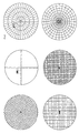
도 3은 다양한 맵핑 형태를 도시한 도면이며, Figure 3 is a diagram illustrating various mapping forms,
도 4는 다수의 예시적 전해연마 모듈에 연결된 예시적 제어 시스템을 도시한 도면이고, 4 is a diagram illustrating an exemplary control system coupled to a number of exemplary electropolishing modules,
도 5는 다수의 서브 시스템을 통하여 다수의 예시적 전해연마 모듈에 연결된 예시적 제어 시스템을 도시한 도면이며, Figure 5 illustrates an exemplary control system coupled to multiple exemplary electropolishing modules through multiple subsystems,
도 6a 내지 도 6d는 예시적 다마신 프로세스를 도시한 도면이고, Figures 6A-6D illustrate an exemplary damascene process,
도 7a 내지 도 7d는 다른 예시적 다마신 프로세스를 도시한 도면이며, Figures 7a-7d illustrate another exemplary damascene process,
도 8a 내지 도 8d는 또 다른 예시적 다마신 프로세스를 도시한 도면이고, Figures 8A-8D are diagrams illustrating another exemplary damascene process,
도 9a 내지 도 9d는 또 다른 예시적 다마신 프로세스를 도시한 도면이다. Figures 9a-9d illustrate another exemplary damascene process.
이하, 많은 특정 구조, 변수 등이 개시되어 있다. 그러나, 하기된 설명은 본 발명의 범위를 제한하고자 하는 것이 아니며, 예시적 실시예를 설명하고자 하는 것임을 이해할 수 있을 것이다. Hereinafter, many specific structures, variables and the like are disclosed. It should be understood, however, that the description below is not intended to limit the scope of the invention, but is intended to be illustrative of the exemplary embodiments.
Ⅰ. 적정 전해연마Ⅰ. Proper electrolytic polishing
전술한 바와 같이, 반도체 웨이퍼상에 트랜지스터 및 인터커넥션 소자를 형성함에 있어서, 상기 반도체 웨이퍼상에 금속이 증착되었다가 제거된다. 더욱 상세하게, 금속의 층(즉, 금속층)이 화학기상증착(CVD), 물리기상증착(PVD), 원자층증착(ALD), 전기도금, 무전해 도금 등과 같은 증착 프로세스를 사용하여 반도체 웨이퍼상에 형성된다. 그 다음, 상기 금속층은 화학적 기계적 폴리싱(CMP), 전해연마 등과 같은 에칭 또는 폴리싱 프로세스를 사용하여 제거된다. As described above, in forming the transistor and the interconnection element on the semiconductor wafer, the metal is deposited on the semiconductor wafer and removed. More specifically, a layer of metal (i.e., a metal layer) is deposited on a semiconductor wafer using a deposition process such as chemical vapor deposition (CVD), physical vapor deposition (PVD), atomic layer deposition (ALD), electroplating, electroless plating, As shown in FIG. The metal layer is then removed using an etching or polishing process such as chemical mechanical polishing (CMP), electrolytic polishing, and the like.
도 1을 참조하면, 일 실시예에서, 반도체 웨이퍼(102)상에 형성된 금속층을 제거/폴리싱하기 위해 전해연마 모듈(100)이 사용될 수 있다. 본 실시예에서, 웨이퍼(102)는 웨이퍼 척(112)에 의해 유지되며, 상기 웨이퍼 척은 세타(Θ) 각을 중심으로 웨이퍼(102)를 회전시키며 도 1에 도시된 x방향과 같은 측방향으로 웨이퍼(102)를 이동시킨다. 웨이퍼 척(112)에 의해 웨이퍼가 회전 및 이동하는 동안, 노즐(108) 및/또는 노즐(110)을 통하여 웨이퍼(102)상에 형성된 금속층에 전해액이 도포된다. 도 1에 도시된 바와 같이, 노즐(108)은 노즐(110)보다 더 좁은 전해액 스트림을 제공하도록 구성될 수 있다. 따라서, 노즐(108)은 노즐(110)보다 더 정밀한 폴리싱을 위해 사용될 수 있다. 예를 들어, 노즐(110)은 웨이퍼(102)의 표면으로부터 초기량의 금속층이 폴리싱되는 초기 거친 폴리싱(initial rough polishing)을 위해 사용될 수 있으며, 그 다음, 초기 거친 폴리싱에서보다 금속층이 더 균일하게 폴리싱되는 후속 미세 폴리싱을 위해 노즐(108)이 사용될 수 있다. 본 실시예에서, 웨이퍼(102) 표면상의 금속층의 두께를 측정하기 위해 종점 검출기 (106)가 사용될 수 있다. 도 1에서, 종점 검출기(106), 노즐(108) 및 노즐(110)은 노즐 플레이트(104)상에 서로 근접하도록 배치된 것으로 도시되어 있다. 그러나, 종점 검출기(106), 노즐(108) 및 노즐(110)은 다양한 구성으로 배치되어 다양한 방식으로 장착될 수 있음을 이해하여야 한다. 또한, 하나의 노즐을 포함하여 임의 갯수의 노즐이 웨이퍼(102)상의 금속층을 전해연마하기 위해 사용될 수 있음을 이해하여야 한다. 또한, 웨이퍼 척(112)을 이용하여 웨이퍼(102)를 이동시키는 대신 또는 이에 부가하여, 종점 검출기(106), 노즐(108) 및/또는 노즐(110)을 이동시키는 것도 가능함을 이해하여야 한다. Referring to FIG. 1, in one embodiment, an
예시적인 전해연마 프로세스 및 시스템의 보다 상세한 설명을 위하여, "반도체 장치상의 금속 인터커넥션을 전해연마하기 위한 장치 및 방법"이란 명칭으로 1999년 7월 2일자에 출원된 미국특허 제6,394,152B1호; "반도체 공작물의 전해연마 및/또는 전기도금 과정에서 반도체 공작물을 유지 및 위치결정하기 위한 장치 및 방법"이란 명칭의 미국특허 제6,248,222B1호; 및 "전해연마 및/또는 전기도금 장치 및 방법"이란 명칭으로 2002년 4월 14일자에 출원된 미국 가출원 제60/372,566호를 참조하기 바라며, 본원은 이들의 내용 전체를 참조하였다. 예시적인 종점 검출기의 보다 상세한 설명을 위하여, "종점 검출 장치 및 방법"이란 명칭으로 2000년 5월 12일자에 출원된 미국특허 제6,447,668호를 참조하기 바라며, 본원은 그 내용 전체를 참조하였다. For a more detailed description of an exemplary electrolytic polishing process and system, reference is made to U.S. Patent No. 6,394,152 B1, filed July 2, 1999, entitled "Apparatus and Method for Electropolishing Metal Interconnection on Semiconductor Devices" U.S. Patent No. 6,248,222 B1, entitled " Apparatus and Method for Maintaining and Positioning a Semiconductor Workpiece During Electrolytic Polishing and / or Electroplating of a Semiconductor Workpiece "; And US Provisional Application No. 60 / 372,566, filed April 14,2002, entitled " Electrolytic Polishing and / or Electroplating Apparatus and Method ", the entire contents of which are incorporated herein by reference. For a more detailed description of an exemplary endpoint detector, reference is made to U.S. Patent No. 6,447,668, entitled " Endpoint Detection Apparatus and Method, " filed May 12, 2000, the disclosure of which is incorporated herein by reference in its entirety.
본 실시예에서, 일반적으로, 웨이퍼는 액체 유동율, 전류 또는 전압 설정값, 중심대 엣지의 거리, 초기 회전속도, 폴리싱 시간, 중심 폴리싱 회전속도, 노즐의 유형, 전류 또는 전압 테이블, 정전류용 벌크율 테이블, 반복 설정값 등과 같은 다양한 프로세싱 변수를 포함하는 방법을 이용하여 프로세싱된다. 동일한 증착 프로세스를 이용하여 프로세싱된 웨이퍼는 일반적으로 유사한 금속층 두께 프로파일을 갖기 때문에, 웨이퍼는 유사한 폴리싱 방법을 이용하여 초기에 폴리싱될 수 있다. In this embodiment, in general, the wafer may include a liquid flow rate, current or voltage set point, center-to-edge distance, initial rotational speed, polishing time, central polishing rotational speed, nozzle type, current or voltage table, Tables, repetitive set values, and the like. Because the wafers processed using the same deposition process generally have similar metal layer thickness profiles, the wafers may be polished initially using a similar polishing method.
그러나, 전술한 바와 같이, 웨이퍼상에 형성된 금속층을 폴리싱함에 있어서, 금속층을 너무 과도하게 또는 너무 불충분하게 폴리싱하면, 반도체 장치가 제대로 작동하지 않는 결과를 유발할 수 있다. 따라서, 본 실시예에서, 금속층의 적정 전해연마를 위해 웨이퍼상의 금속층 두께가 이용된다. 특히, 웨이퍼상에 형성된 금속층의 일부를 전해연마하기에 앞서, 전해연마하고자 하는 부분의 두께가 측정되며, 전해연마될 부분의 양이 측정된 두께에 기초하여 조절된다. However, as described above, in polishing a metal layer formed on a wafer, if the metal layer is polished too much or too poorly, the semiconductor device may fail to work properly. Therefore, in this embodiment, the thickness of the metal layer on the wafer is used for proper electrolytic polishing of the metal layer. Particularly, before electrodepositing a part of the metal layer formed on the wafer, the thickness of the portion to be electrolytically polished is measured, and the amount of the portion to be electrolytically polished is adjusted based on the measured thickness.
예를 들어, 제어 시스템(114)이 웨이퍼 척(112) 및 노즐(108) 및 노즐(110)에 연결될 수 있다. 웨이퍼 척(112)의 위치에 기초하여, 상기 제어 시스템(114)은 전해연마하고자 하는 웨이퍼(102)상의 금속층의 부분의 위치를 결정할 수 있다. 상기 제어 시스템(114)은 전해연마하고자 하는 금속층의 부분의 두께를 측정하고, 노즐(108) 및/또는 노즐(110)에 의해 전해연마되는 부분의 양을 조절한다. For example, the
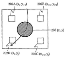
일 실시예에서, 웨이퍼(102)가 폴리싱 모듈(100)에서 프로세싱되기 전에, 웨이퍼(102)상의 금속층의 두께를 측정하고 맵핑하기 위해 기판 두께 계측툴(116)가 사용된다. 도 2a를 참조하면, 계측툴(도 1)은 웨이퍼(102)상의 다양한 위치(202)에서의 두께를 측정할 수 있다. 위치(202)는 다양한 좌표계를 이용하여 맵핑될 수 있다. 예를 들어, 도 2a에 도시된 바와 같이, 단순한 xy 좌표축이 사용될 수 있 다. 선택적으로, 웨이퍼(102)의 회전 각도에 대응하는 각도(Θ)와 반경이 사용될 수 있다. 그 후, 제어 시스템(도 1)이 웨이퍼(102)상의 금속층의 두께의 맵핑을 이용하여 전해연마하기에 전에 금속층 부분의 두께를 구할 수 있다. In one embodiment, a substrate
도 2a에 도시된 바와 같이, 웨이퍼(102)상의 금속층 두께의 맵핑은 금속층의 두께가 알려지지 않은 위치를 의미하는 갭(gaps)을 포함할 수 있다. 특히, 웨이퍼(102)의 회전 및 이동으로 인하여, 전해액 스트림은 노즐(108)(도 1) 및/또는 노즐(110)(도 1)에 의해 나선형 경로(204)로 제공될 수 있다. 또한, 도 2a에 도시된 바와 같이, 전해액 스트림은 금속층의 두께가 알려지지 않은 위치(206)에 제공될 수 있다. 따라서, 본 실시예에서는, 위치(206)에서의 금속층의 두께를 결정하기 위하여, 금속층의 두께가 알려진 2개 또는 그 이상의 위치(202)로부터 측정된 두께가 사용된다. As shown in FIG. 2A, the mapping of the thickness of the metal layer on the
예를 들어, 도 2b에 도시된 바와 같이, 위치(206)에서의 금속층 두께는 위치(202A,202B,202C,202D)에서의 금속층 두께에 기초하여 결정된다. 도 2a에서 사용된 xy 좌표계에 따르면, 위치(206)는 지점(x,y)에 대응하고, 위치(202A)(202B)(202C)(202D)는 각각 지점(xi,yj+1)(xi+1,yj+1)(x
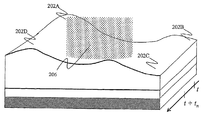
i+1,yj)(xi,yj)에 대응한다. 도 2c는 금속층의 두께 변화를 사시도로서 도시하고 있다. For example, as shown in FIG. 2B, the metal layer thickness at
본 실시예에서, 위치(206)에서의 금속층 두께는 하기된 식에 의해 특정되는 것으로 가정한다. In this embodiment, it is assumed that the thickness of the metal layer at the
T=Ax+By+Cxy+D (식 1) T = Ax + By + Cxy + D (Equation 1)
또한, (xi,yj)에서의 두께(Ti,j), (xi,yj+1)에서의 두께(Ti,j+1), (xi+1,yj)에서의 두께(Ti+1,j), 및 (xi+1,yj+1)에서의 두께(Ti+1,j+1)는 하기된 식에 의해 특정되는 것으로 가정한다. Also, (x i, y j) in the thickness (T i, j), ( x i, y j + 1) the thickness (T i, j + 1) , (x i + 1, y j) in at the thickness (T i + 1, j) , and thickness (T i + 1, j + 1) at (x i + 1, y j + 1) of is assumed to be specified by the following formula.
Ti,j=Axi+Byj+Cxiyj+D (식 2) I T, i j = Ax + By + Cx j y i j + D (Equation 2)
Ti,j+1=Axi+Byj+1+Cxiyj+1+D (식 3) T i, j + 1 = Ax i + By j + 1 + Cx i y j + 1 + D ( formula 3)
Ti+1,j=Axi+1+Byj+Cxi+1yj+D (식 4) T i + 1, j = Ax i + 1 + By j + Cx i + 1 y j + D ( Equation 4)
Ti+1,j+1=Axi+1+Byj+1+C (식 5)T i + 1, j + 1 = Ax i + 1 + By j + 1 +
그 다음, 하기된 방식으로 식 2 내지 식 5를 풀어 A,B,C,D값을 구할 수 있다. Then, the values A, B, C, and D can be obtained by solving
C=(Ti,j-Ti,j+1-Ti+1,j+Ti+1,j+1)/[(xi-xi+1 )*(yj-yj+1)] C = (T i, j -T i, j + 1 -T i + 1, j + T i + 1, j + 1) / [(x i -x i + 1) * (y j -y j + 1 )]
B=(Ti,j-Ti,j+1)/(yj-yj+1)-xi*DB = (T i, j -T i, j + 1 ) / (y j -y j + 1 ) -x i * D
A=(Ti,j-Ti+1,j)/(xi-xi+1)-yj*DA = (T i, j -T i + 1, j ) / (x i -x i + 1 ) -y j * D
D=Ti,j-xi*B-yj*[(Ti,j-Ti,j+1)/(yj-y j+1)] D = T i, j -x i * By j * [(T i, j -T i, j + 1) / (y j -y j + 1)]
위치(206)에서의 금속층 두께를 결정하기 위하여, 금속층의 두께가 알려진 임의 갯수의 위치(202)가 사용될 수 있음을 알 수 있다. 예를 들면, 전술한 것보다 더 정확한 보간(interpolation)을 위하여, 위치(206)에서의 금속층 두께는 하기된 식에 의해 특정되는 것으로 가정할 수 있다.
It will be appreciated that in order to determine the thickness of the metal layer at
T=Ax2+By2+Cxy+Dx+Ey+F (식 7) T = Ax 2 + By 2 + Cxy + Dx + Ey + F ( formula 7)
(x,y)에서의 두께(T)는 위치(206)와 가장 인접한 6개의 위치를 이용하여 보간될 수 있으며, 계수(A,B,C,D,E,F)는 전술한 4개의 위치에서 계수(A,B,C,D)를 구한 것과 동일한 방식으로 6개의 등식을 풀어서 구할 수 있다. A, B, C, D, E, and F may be interpolated using the six positions closest to the
다시 도 1을 참조하면, 본 실시예에서, 종점 검출기(106)를 이용하여 웨이퍼(102)상의 금속층 두께를 구할 수 있다. 특히, 노즐(108) 및/또는 노즐(110)을 이용하여 웨이퍼(102)를 전해연마하는 것과 동일한 방식으로 종점 검출기(106)에 인접하여 웨이퍼(102)를 회전 및 이동시킬 수 있다. 따라서, 노즐(108) 및/또는 노즐(110)을 이용하여 웨이퍼(102)를 전해연마하는 것과 동일한 경로(204)(도 2)를 따라 웨이퍼(102)상의 금속층의 두께를 측정할 수 있다. Referring again to Figure 1, in this embodiment, the thickness of the metal layer on the
예를 들어, 종점 검출기(106)가 광학 센서인 경우, 웨이퍼(102)가 회전 및 이동할 때, 종점 검출기(106)에 인접한 웨이퍼(102) 표면의 반사율이 기록될 수 있다. 그 다음, 위치(206)(도 2)와 같은 위치에서의 금속층 두께가 하기된 식을 이용하여 계산될 수 있다. For example, when the
T(x,y)=P(T)*R(x,y) (식 7)T (x, y) = P (T) * R (x, y)
여기서, R(x,y)은 종점 검출기(106)에 의해 측정된 위치(206)(도 2)에서의 금속 필름의 반사율이고, P(T)는 두께에 대한 반사율의 환산인자로서, 그 자체가 두께의 함수이다. P(T)는 알려진 다양한 두께를 가진 금속층 세트를 이용하여, 그 알려진 두께를 금속층의 반사율과 상호연관시킴으로써 결정될 수 있다. 결정된 환 산인자(P(T))는 두께가 알려지지 않은 금속층의 반사율에 대응하는 두께를 결정하기 위해 사용될 수 있다. Here, R (x, y) is the reflectance of the metal film at the position 206 (FIG. 2) measured by the
선택적으로, 알려진 두께와 해당 반사율은 제어 시스템(114)과 같은 컴퓨터에서 탐색표(lookup table)에 저장될 수 있다. 예를 들면, 상기 탐색표는 하기된 바와 같이 컴퓨터 메모리에 저장된 두께 행렬을 포함할 수 있다. Alternatively, the known thickness and the reflectivity may be stored in a lookup table in a computer, such as the
T1,1 T1,2 T1,3 ... T1,m T 1,1 T 1,2 T 1,3 ... T 1, m
T2,1 T2,2 T2,3 ... T2,m T 2,1 T 2,2 T 2,3 ... T 2, m
T3,1 T3,2 T3,3 ... T3,m T 3,1 T 3,2 T 3,3 ... T 3, m
........
Tn,1 Tn,2 Tn,3 ... Tn,m T n, 1 T n, 2 T n, 3 ... T n, m
여기서, 상기 두께 행렬내의 각 두께는 해당 반사율을 갖는다. Here, each thickness in the thickness matrix has a corresponding reflectance.
종점 검출기(106)를 이용하여 위치(206)(도 2)에서의 반사율을 측정한 후, 제어 시스템(114)이 환산인자(P(T)) 또는 탐색표를 이용하여 두께(T(x,y))를 결정할 수 있다. 금속 층은 두께 측정을 이용하여 전해 연마될 수 있다. 상기 프로세스는 종점 검출기(106)에 의해 기록된 반사율이 예비설정범위내에 놓일 때까지 반복될 수 있다. 상기 반사율의 예비설정범위는 금속 패턴 밀도, 과연마 범위 등과 같은 다양한 인자에 따라 좌우된다. 일반적으로, 패턴 밀도가 낮으면 낮을수록, 반사율 예비설정값은 더 낮아진다. 또한, 예비설정된 반사율은 패턴 밀도에 기초하여 변할 수 있다. 상기 예비설정된 반사율은 마스크의 패턴 밀도에 기초하여 계산되거나, 또는 최소 금속 리세스를 구비한 하나의 폴리싱된 웨이퍼에 의해 측정될 수 있다. 상기 예비설정된 반사율의 보다 상세한 설명을 위하여, "종점 검출 장치 및 방법"이란 명칭으로 2000년 5월 12일자에 출원된 미국특허 제6,447,668호를 참조하기 바라며, 본원은 그 내용 전체를 참조하였다. After the
상기 종점 검출기(106)가 다양한 유형의 센서일 수 있음을 이해하여야 한다. 예를 들면, 종점 검출기(106)는 맴돌이 전류(Eddy Current) 센서일 수 있다. 따라서, 종점 검출기(106)는 반사율보다는 맴돌이 전류를 측정하기 위해 사용되며, 상기 금속층의 두께는 측정된 반사율보다는 측정된 맴돌이 전류에 기초하여 결정된다. It should be understood that the
종점 검출기(106)를 이용한 두께 측정이 금속층이 전해연마되는 경로와 동일한 경로를 따르기 때문에, 두께 측정값에서의 갭은 여전히 존재한다. 예를 들어, 두께 측정은 처리량을 증대시키기 위하여 연속적이 아닌 인터벌을 두고 이루어진다. 두께 측정값에서 갭이 존재하는 경우, 두께 측정값이 알려지지 않은 위치에서의 두께를 구하기 위하여, 전술한 보간 프로세스가 사용될 수 있다. Since the thickness measurement using the
또한, 본 실시예에서, 웨이퍼상의 임의의 지점을 맵핑 및 위치결정하기 위해 격자 영상법(grid by grid imaging)이 사용될 수 있다. 특히, 웨이퍼의 표면이 화소 구획(pixel partitions)으로 맵핑될 수 있으며, 여기서 각각의 화소 구획은 종점 검출기(106)(도 1)를 이용하여 측정될 수 있는 필드에 대응한다. 도 3은 다양한 예시적 화소 구획을 도시한 도면이다. 종점 검출기(106)(도 1)는 웨이퍼의 중심으로부터 시작하여 웨이퍼의 엣지까지 또는 엣지로부터 중심까지 바람직하게는 크기가 2.5㎜×2.5㎜인 주어진 지점(x,y) 또는 화소에 대한 반사율을 측정할 수 있 다. 종점 검출기(106)(도 1)는 하나의 화소로부터 이동하여, 200㎜ 웨이퍼에 대하여 최대 11,494개의 모든 화소(즉, πR2/(2.5)2)가 기록될 때까지, 각 화소에 대한 반사율 데이타를 동시에 기록할 수 있다. Also, in this embodiment, grid by grid imaging may be used to map and locate any point on the wafer. In particular, the surface of the wafer may be mapped to pixel partitions, where each pixel segment corresponds to a field that can be measured using the endpoint detector 106 (Fig. 1). Figure 3 is a diagram illustrating various exemplary pixel sections. The endpoint detector 106 (FIG. 1) measures the reflectance for a given point (x, y) or pixel, preferably starting from the center of the wafer to the edge of the wafer or from the edge to the center, preferably 2.5 mm x 2.5 mm can do. The endpoint detector 106 (FIG. 1) moves from one pixel until the maximum of 11,494 pixels (i.e.,? R 2 /(2.5) 2 ) is recorded for a 200 mm wafer, Can be recorded at the same time.
본 실시예에서, 웨이퍼를 전해연마하기 전에, 기판 두께 계측툴로부터 얻은 초기 두께 측정값을 이용하여 초기 거친 전해연마를 실시한다. 상기 초기 거친 전해연마가 완료된 후, 예를 들어 종점 검출기를 이용하여 금속층의 중간 두께 측정값이 얻어진다. 그 다음, 상기 중간 두께 측정값을 이용하여 금속층을 다시 전해연마하게 된다. 상기 금소층의 두께가 약 1000Å과 같은 한계값 이하인 경우, 상기 초기 거친 전해연마는 종료될 수 있다. 그러나, 상기 금속층이 중간 두께 측정값없이 초기 두께 측정값에 기초하여 전해연마될 수 있음을 이해하여야 한다. 선택적으로, 상기 금속층은 예를 들어 초기 두께 측정값없이 종점 검출기를 이용하여 얻어진 두께 측정값에 기초하여 전해연마될 수 있다. In the present embodiment, before the electrolytic polishing of the wafer, the initial rough electrolytic polishing is performed using the initial thickness measurement value obtained from the substrate thickness measurement tool. After the initial rough electrolytic polishing is completed, an intermediate thickness measurement value of the metal layer is obtained, for example, by using an end point detector. The metal layer is then again electrolytically polished using the intermediate thickness measurements. If the thickness of the gold layer is below a threshold value such as about 1000 angstroms, the initial rough electrolytic polishing may be terminated. However, it should be understood that the metal layer may be electropolished based on the initial thickness measurements without intermediate thickness measurements. Alternatively, the metal layer may be electropolished based on thickness measurements obtained using an endpoint detector, for example, without an initial thickness measurement.
전술한 바와 같이, 본 실시예에서, 전해연마되는 금속층 부분의 양은 상기 부분의 두께 측정값에 기초하여 조절된다. 전해연마되는 금속층 부분의 양은 그 부분에 제공되는 전해액 스트림에 인가되는 전류 및/또는 전압을 변경함으로써 조절될 수 있다. 예를 들어, 인가되는 폴리싱 전류는 하기된 바와 같이 두께에 기초하여 결정될 수 있다. As described above, in this embodiment, the amount of the metal layer portion to be electrolytically polished is adjusted based on the thickness measurement value of the portion. The amount of metal layer portion to be electrolytically polished can be controlled by changing the current and / or voltage applied to the electrolyte stream provided to that portion. For example, the applied polishing current may be determined based on the thickness as follows.
I=kT(x,y) (식 7)I = kT (x, y) (Equation 7)
여기서, k는 폴리싱 속도와 연관된 인자이다. 전해액 스트림에 인가되는 전 류 및/또는 전압을 변경함과 아울러, 상기 부분에 전해액 스트림이 제공되는 시간의 양(즉, 폴리싱 시간)이 상기 부분의 두께 측정값에 기초하여 조절될 수 있다. 더욱이, 상기 부분의 두께 측정값에 기초하여 전류, 전압 및 폴리싱 시간의 임의의 조합이 조절될 수 있다. Where k is a factor associated with the polishing rate. The amount of time (i.e., polishing time) that the electrolyte stream is provided to the portion, as well as changing the current and / or voltage applied to the electrolyte stream, can be adjusted based on the thickness measurement of the portion. Moreover, any combination of current, voltage and polishing time can be adjusted based on the thickness measurement of the part.
따라서, 도 1을 참조하면, 본 실시예에서, 제어 시스템(114)은 전해연마하고자 하는 금속층의 부분의 두께 측정값을 결정한 다음, 결정된 두께 측정값에 기초하여 전해연마되는 부분의 양을 조절하게 된다. 전술한 바와 같이, 상기 제어 시스템(114)은 노즐(108) 및/또는 노즐(110)에 의해 제공되는 전해액 스트림에 인가되는 전류 및/또는 전압을 조절할 수 있다. 또한, 상기 제어 시스템(114)은 웨이퍼 척(112)의 회전 및/또는 이동 속도를 조절함으로써 폴리싱 시간을 조절할 수 있다. 1, in this embodiment, the
본 실시예에서, 상기 제어 시스템(114)이 조절하기로 결정하는 시간으로부터 조절이 이루어지는 시간까지의 지연량(즉, △t)은, 상기 부분이 전해연마되기 전에 제어 시스템(114)이 금속층 부분에 대한 조절을 결정하기에 앞서는 오프셋 시간으로 사용된다. 예를 들면, 노즐(108)에 의해 제공되는 전해액 스트림에 인가되는 전류를 금속층 부분에 대해 조절하고자 하는 경우, 상기 제어 시스템(114)은 전해연마하고자 하는 부분에 도달하는 노즐(108)의 적어도 오프셋 시간(즉, △t)만큼 전류가 먼저 인가되도록 결정한다. In this embodiment, the amount of delay (i.e., DELTA t) from the time the
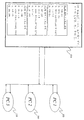
이하, 도 4를 참조하면, 제어 시스템(114)은 다수의 전해연마 모듈(100)(예를 들어, 프로세싱 챔버 1(PC1), PC2 및 PC3)에 연결될 수 있다. 도 4에 도시된 바와 같이, 제어 시스템(114)은 각각의 전해연마 모듈(100)에 대한 프로세스 제어를 실시한다. 예를 들어, 각각의 전해연마 모듈(100)에 대하여, 제어 시스템(114)은 폴리싱 방법, 두께 측정값(예를 들어, 반사율 데이타) 기록, 두께 측정값 프로세싱 및 금속 필름 두께 프로파일 업로딩, 전해연마 조절(예를 들어, 노즐에 의해 제공되는 전해액 스트림에 인가되는 전류 또는 전압의 조절) 및 전해연마하고자 하는 각 웨이퍼에 대한 폴리싱 방법 반복을 실시한다. 또한, 제어 시스템(114)은 그래픽 사용자 인터페이스, 웨이퍼 핸들링, 경보 관리 등 다양한 추가 작업을 실시한다. 4, the
그러나, 제어 시스템(114)에 요구되는 프로세싱 및 연산 부하는 판독(read-outs), 전기적 출력 및 기계적 운동과 같은 일에 대한 응답시간을 줄일 수 있다. 제어 시스템(114)의 핸들링에 필요한 부하의 수를 증가시킴으로써, 각 부하에 대한 완료 시간(completion time)을 줄일 수 있다. 따라서, 본 실시예에서, 제어 시스템(114)은 분산된 다수의 서브 시스템을 포함하며, 과업지향형 기능(task-oriented functions)은 모션 서버 블록 제어기와 같은 개별 서브 시스템으로 배분(offloaded)된다. However, the processing and computational load required of the
특히, 도 5를 참조하면, 하나의 서브 시스템(502)이 하나의 전해연마 모듈(100)(예를 들어, PC1, PC2 또는 PC3)에 대하여 전용화되어 있다. 도 5에 도시된 분산형 서브 시스템은 도 4에 도시된 집중식 시스템과 관련된 시간 지체(time lag)를 줄인다. 도 5에 도시된 실시예에서, PC 기반 제어 시스템(114)은 RS-485, DeviceNet 등과 같은 장치대 장치 전송매체(504)를 이용하여 각각의 서브 시스템 (502)에 대하여 데이타를 송수신한다. 5, one
예를 들어, 각각의 서브 시스템(502)은 각각의 전해연마 모듈(100)에 대하여 동일한 일을 수행할 수 있다. 도 5에 도시된 바와 같이, 하나의 서브 시스템(502)은 척, 모터 드라이브, 노즐 및 종점 검출기를 작동시키고, PC1에 대한 디지탈 IO 및 아날로그 IO의 데이타를 프로세싱하도록 전용화될 수 있다. 동시에, 다른 서브 시스템(502)은 자신의 개별 전해연마 모듈(100)에 대하여 전용화될 수 있다. 예를 들어, 다른 서브 시스템(502)은 척, 모터 드라이브, 노즐 및 종점 검출기를 작동시키고, PC2에 대한 디지탈 IO 및 아날로그 IO의 데이타를 프로세싱하도록 전용화될 수 있다. For example, each
분산형 배치하에서, 각각의 서브 시스템(500)은 기계적 및 전기적 성능(즉, 잔여 금속층을 가진 웨이퍼의 회전각 및 위치를 기록하고, 주어진 위치에 대하여 기록된 반사율에 기초하여 노즐 기능을 4ms 또는 그 이상으로 제어함) 모두에서 더 우수하고 정교한 제어를 제공할 수 있다. 프로세싱 능력이 향상된 각각의 서브 시스템(502)에 의하여, 본 실시예는 더 정교한 폴리싱 제어를 위하여 반사율 데이타에 기초한 방법에서 다른 값 또는 테이블을 추가 또는 외삽할 수 있다. Under a distributed arrangement, each of the subsystems 500 may record mechanical and electrical performance (i. E., The rotation angle and position of the wafer with the remaining metal layer, and the nozzle function based on the recorded reflectance for a given position, Or more), it is possible to provide better and more sophisticated control. With each
더욱이, 서브 시스템(502)에 분배된 웨이퍼 전해연마의 분산형 프로세싱 조건으로 인하여, 제어 시스템(114)과 서브 시스템(502)은 다른 일을 수행함에 있어서 이용가능한 프로세싱 능력을 가질 수 있다. 특히, 추가적인 툴 및/또는 어플리케이션이 툴 구조의 속도 또는 실용성이 감소되지 않고 폴리싱 프로세스에 부가될 수 있다. 예를 들면, 웨이퍼가 전해연마 모듈에 로딩되기 전에 각 웨이퍼의 프로 파일을 측정하기 위해, 인라인 계측툴이 부가될 수 있다. 상기 인라인 계측툴은 서브 시스템(502) 또는 제어 시스템(114)에 대하여 웨이퍼상의 금속층의 두께를 측정하여 보다 평탄하고 균일한 금속 표면을 얻기 위해 필요한 전류 출력을 결정할 수 있다. 그 후, 상기 서브 시스템(502) 또는 제어 시스템(114)은 거리에 대한 전류 속도 시간 사용자 설정값과 같은 데이타를 가진 새로운 테이블을 만들수 있다. Moreover, due to the distributed processing conditions of the wafer electropolished polished to the
Ⅱ. 장벽층 및 희생층의 제거Ⅱ. Removal of barrier and sacrificial layers
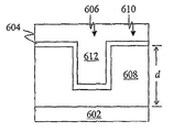
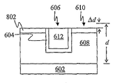
도 6a 내지 도 6d는 반도체 장치내에 인터커넥션을 형성하기 위해 사용될 수 있는 예시적 다마신 프로세스를 도시하고 있다. 특히, 도 6a를 참조하면, 반도체 장치는 리세스 영역(606)과 비 리세스 영역(610)을 가진 유전재료(608)를 포함하며, 상기 리세스 영역(606)은 넓은 트렌치, 대형의 직사각형 구조 등과 같은 구조일 수 있다. CVD, PVD, ALD 등과 같은 임의의 통상의 증착방법에 의해 유전재료(608)상에 장벽층(604)이 증착될 수 있으며, 따라서 상기 장벽층(604)은 리세스 영역(606)과 비 리세스 영역(610)을 모두 덮게 된다. 유전재료 및 장벽층의 보다 상세한 설명을 위하여, "구리를 초저 유전율 재료로 통합하는 방법"이란 명칭으로 2003년 3월 14일자에 출원된 미국특허출원 제10/380,848호; 동일한 명칭으로 2001년 4월 24일자에 출원된 미국 가출원 제60/286,273호를 우선권 주장하며 "더미 구조를 갖춘 트렌치 또는 비아를 구비한 웨이퍼상에서의 금속층 전해연마"란 명칭으로 2002년 3월 27일자에 출원된 미국특허출원 제10/108,614호를 참조하기 바란다. 본원은 이들의 내용 전체를 참조하였다. 6A-6D illustrate an exemplary damascene process that may be used to form an interconnection in a semiconductor device. 6A, a semiconductor device includes a
본 예시적 프로세스에서, 도 6b를 참조하면, PVD, CVD, ALD, 전기도금, 무전 해 도금 등과 같은 임의의 통상의 방법으로 장벽층(604)상에 금속층(612)이 증착될 수 있다. 그 다음, 도 6c를 참조하면, CMP, 전해연마 등을 이용하여 금속층(612)이 폴리싱되며, 따라서, 금속층(612)는 비 리세스 영역(610)으로부터 제거되는 반면, 금속층(612)은 리세스 영역(606)에 남게 된다. 상기 금속층(612)은 구리, 알루미늄, 니켈, 크롬, 아연, 카드뮴, 은, 금, 로듐, 파라듐, 플레티늄, 주석, 납, 강철, 인듐, 초전도체 재료 등과 같은 다양한 전기적 전도성 재료를 포함할 수 있다. 또한, 상기 금속층(612)은 상기 다양한 전기적 전도성 재료중 임의의 합금 또는 초전도체 재료의 화합물을 포함할 수 있다. 바람직하게, 상기 금속층(612)은 구리와 그 합금을 포함한다. 6B, a
이하, 도 6d를 참조하면, 비 리세스 영역(610)으로부터 금속층(612)을 제거한 후, 습식 에칭, 건식 화학 에칭, 건식 플라즈마 에칭 등과 같은 임의의 통상의 방법에 의해 비 리세스 영역(610)으로부터 장벽층(604)이 제거될 수 있다. 비 리세스 영역(610)으로부터 장벽층(604)을 완전히 제거하기 위해, 과에칭이 필요하다. 그러나, 도 6d에 도시된 바와 같이, 과에칭은 노치(614)를 형성할 수 있다. 본 예시적 프로세스에서 SiN 등과 같은 커버층이 증착되는 경우, 상기 노치(614)는 공동이 될 수 있으며, 이는 금속 누설(metal bleeding)로 이어질 수 있다. 누설된 금속은 유전재료(608)를 통하여 장치의 게이트 영역으로 확산될 수 있으며, 이에 따라 반도체 장치가 제대로 작동하지 않게 된다. 6D, after removing the
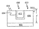
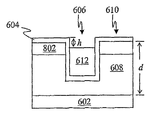
도 7a 내지 도 7d에 도시된 바와 같이, 이러한 문제점을 해결하기 위하여, 전해연마와 플라즈마 에칭을 이용한 과폴리싱의 조합이 사용될 수 있다. 본 예시 적 프로세스에서, 도 7a를 참조하면, 리세스 영역(606)의 금속층(612)이 전해연마, 습식 에칭 등으로 과폴리싱됨으로써, 리세스 영역(606)내의 금속층(612) 표면과 장벽층(604)의 상부간에 h 미크론의 높이가 존재하게 되며, 여기서 상기 높이 h는 장벽층(604)의 두께보다 크거나 같다. 습식 에칭방법과 비교하여 리세스 영역(606)의 금속층(612)을 과폴리싱하고자 할 때, 전해연마는 양호하게 제어되기 때문에 프로세스 문제를 덜 야기함을 이해하여야 한다. 전해연마의 설명을 위하여, "반도체 장치상의 금속 인터커넥션을 전해연마하는 장치 및 방법"이란 명칭으로 1999년 7월 2일자에 출원된 미국특허 제6,395,152호를 참조하기 바라며, 본원은 그 내용 전체를 참조하였다. As shown in Figs. 7A to 7D, in order to solve this problem, a combination of over polishing using electrolytic polishing and plasma etching can be used. 7A, the
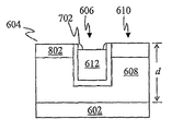
그 다음, 도 7b를 참조하면, CF4/O2, SF6/O2 등과 같은 첨가제가 에칭 가스, Ta, C 및 F에 첨가됨으로써, 리세스 영역(606)내의 금속층(612) 및 장벽층(604)에 잔류물(702)을 형성하게 된다. 도 7c에 도시된 바와 같이, 장벽층(604)이 에칭될 때, 잔류물(702)은 리세스 영역(606)내의 금속층(612)과 유전재료(608) 사이의 장벽층(604)이 과에칭되는 것을 막아준다. Next, Referring to Figure 7b, CF 4 / O 2, SF 6 /
하기된 표 1에는 장벽층(604)을 제거하기 위해 플라즈마 건식 에칭 프로세스에 채용될 수 있는 예시적인 변수의 범위를 제공한다. Table 1 below provides a range of exemplary parameters that can be employed in a plasma dry etch process to remove
이들 변수에 따르면, 2개의 가능한 장벽층(604) 재료인 TaN 및 TiN의 제거율이 가능한 유전재료(608)인 SiO2 제거율에 가깝다. 선택도는 장벽층(604)의 제거 과정에서 하부의 유전재료(608)에 대한 손상 또는 에칭을 줄이는 방식으로 선택된다. 그러나, 상기 변수들을 변화시킴으로써 다른 선택도가 얻어질 수 있음을 이해하여야 한다. According to these variables, the removal rates of the two
이하, 도 7d를 참조하면, 플라즈마 에칭 프로세스 또는 건식 화학 크린닝 또는 임의의 다른 통상의 프로세스에 의해 리세스 영역(606)과 비 리세스 영역(610)의 일부가 약 △d 만큼 제거될 수 있다. 높이에 있어서 장벽층(604)이 유전재료(608)보다 더 높거나 동일하도록 하기 위하여, 장벽층(604)의 에칭율은 유전재료(608)의 에칭율보다 낮거나 동일하도록 설정되어야 한다. 따라서, 다음에 상부층이 증착될 때 공동이 형성되지 않는다. 7D, a portion of the recessed
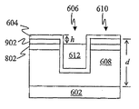
도 8a 내지 도 8d에는 다른 예시적 프로세스가 도시되어 있다. 도 8a 내지 도 8d에 도시된 예시적 프로세스는, 웨이퍼가 606과 같은 리세스 영역을 형성하는 에칭 및 증착 프로세스를 거치기 전에 경질(hard)의 마스크층(802)이 유전재료(608)상에 증착된 것을 제외하고, 도 7a 내지 도 7d에 도시된 프로세스와 많은 점에 있어서 유사하다. 도시된 바와 같이, 경질의 마스크층(802)은 장벽 제거 프로세스과정에서 경질의 마스크층(802)의 하부의 유전재료(608)가 에칭되는 것을 방지할 수 있으며, 따라서 유전체, 특히 저유전율 유전체의 성능 저하를 회피할 수 있다. 리세스(h)는 경질의 마스크(802)의 두께와 장벽층(604)의 두께의 합보다 더 작다. Other exemplary processes are shown in Figures 8A-8D. The exemplary process illustrated in Figures 8A-8D includes depositing a
도 9a 내지 도 9d에는 또 다른 예시적 프로세스가 도시되어 있다. 도 8a 내지 도 8d와 유사하게, 도 9a 내지 도 9d에 도시된 예시적 프로세스는, 경질의 마스크층(802)과 아울러, 상기 경질의 마스크층(802)의 상부에 희생층(902)이 증착된 것을 제외하고, 도 7a 내지 도 7d에 도시된 프로세스와 많은 점에 있어서 유사하다. 본 예시적 실시예에서, 상기 경질의 마스크층(802)은 장벽층(604)보다 더 낮은 제거율을 갖는 반면, 상기 장벽층(604)의 제거율보다 더 크거나 같은 제거율을 가진 희생층(902)이 사용된다. 9A-9D, another exemplary process is shown. Similar to Figs. 8A-8D, the exemplary process illustrated in Figs. 9A-9D includes depositing a
도 8a 내지 도 8d 그리고 도 9a 내지 도 9d 모두에서, 경질의 마스크층(802)은 SiN, SiC, SiO2, SiON, 다이아몬드 필름 등으로부터 선택될 수 있다. 희생층(902)은 SiN, SiO2, SiON 등으로부터 선택될 수 있다. Figures 8a through 8d, and in both Figures 9a through 9d, the
예시적 실시예에 대하여 설명하였으나, 본 발명의 사상 및/또는 범주를 벗어나지 않는 다양한 변형이 이루어질 수 있다. 따라서, 본 발명이 전술한 설명 및 도면에 도시된 특정 형태에 한정되는 것으로 해석되지 않아야 한다.Although an exemplary embodiment has been described, various modifications may be made without departing from the spirit and / or scope of the invention. Accordingly, the invention should not be construed as limited to the specific forms shown in the foregoing description and drawings.
Claims (43)
Applications Claiming Priority (5)
| Application Number | Priority Date | Filing Date | Title |
|---|---|---|---|
| US39794102P | 2002-07-22 | 2002-07-22 | |
| US60/397,941 | 2002-07-22 | ||
| US40399602P | 2002-08-17 | 2002-08-17 | |
| US60/403,996 | 2002-08-17 | ||
| PCT/US2003/022928 WO2004010477A2 (en) | 2002-07-22 | 2003-07-22 | Adaptive electropolishing using thickness measurements and removal of barrier and sacrificial layers |
Publications (2)
| Publication Number | Publication Date |
|---|---|
| KR20050021553A KR20050021553A (en) | 2005-03-07 |
| KR101151456B1 true KR101151456B1 (en) | 2012-06-04 |
Family
ID=30773050
Family Applications (1)
| Application Number | Title | Priority Date | Filing Date |
|---|---|---|---|
| KR1020057001191A Expired - Lifetime KR101151456B1 (en) | 2002-07-22 | 2003-07-22 | Adaptive electropolishing using thickness measurements and removal of barrier and sacrificial layers |
Country Status (9)
| Country | Link |
|---|---|
| US (1) | US20050245086A1 (en) |
| EP (1) | EP1573783A2 (en) |
| JP (2) | JP2006511699A (en) |
| KR (1) | KR101151456B1 (en) |
| CN (1) | CN101427351B (en) |
| AU (1) | AU2003256673A1 (en) |
| CA (1) | CA2491951A1 (en) |
| TW (2) | TW200409223A (en) |
| WO (1) | WO2004010477A2 (en) |
Families Citing this family (17)
| Publication number | Priority date | Publication date | Assignee | Title |
|---|---|---|---|---|
| TW200845162A (en) * | 2006-05-02 | 2008-11-16 | Acm Res Inc | Removing barrier layer using an eletro-polishing process |
| US7667835B2 (en) * | 2006-08-28 | 2010-02-23 | Taiwan Semiconductor Manufacturing Co., Ltd. | Apparatus and method for preventing copper peeling in ECP |
| US20090133908A1 (en) * | 2007-11-28 | 2009-05-28 | Goodner Michael D | Interconnect structure for a microelectronic device, method of manfacturing same, and microelectronic structure containing same |
| KR101492467B1 (en) | 2008-08-20 | 2015-02-11 | 에이씨엠 리서치 (상하이) 인코포레이티드 | Barrier layer removal method and apparatus |
| CN102601471B (en) * | 2012-03-28 | 2013-07-24 | 华南理工大学 | Finish machining method for space curve meshing gear mechanism |
| CN104471690B (en) * | 2012-05-24 | 2017-04-19 | 盛美半导体设备(上海)有限公司 | Method and apparatus for pulse electrochemical polishing |
| JP6186780B2 (en) | 2013-03-18 | 2017-08-30 | 富士通株式会社 | Semiconductor device and manufacturing method thereof |
| CN104952787B (en) * | 2014-03-26 | 2020-03-27 | 盛美半导体设备(上海)股份有限公司 | Automatic radial thickness trimming method |
| JP6301003B2 (en) * | 2014-07-08 | 2018-03-28 | エーシーエム リサーチ (シャンハイ) インコーポレーテッド | Metal wiring formation method |
| CN107258011A (en) | 2014-10-31 | 2017-10-17 | 维克精密表面处理有限责任公司 | Systems and methods for performing a wet etch process |
| CN105300324B (en) * | 2015-09-16 | 2018-06-01 | 浙江工业大学 | A kind of evaluation method of brittle material surface before polishing |
| TWI738757B (en) * | 2016-04-05 | 2021-09-11 | 美商維克儀器公司 | An apparatus and method to control etch rate through adaptive spiking of chemistry |
| EP3590128A1 (en) | 2017-03-03 | 2020-01-08 | Veeco Precision Surface Processing LLC | An apparatus and method for wafer thinning in advanced packaging applications |
| KR102301933B1 (en) * | 2018-12-26 | 2021-09-15 | 한양대학교 에리카산학협력단 | Fabricating method of Semiconductor device |
| CN113604864A (en) * | 2021-06-29 | 2021-11-05 | 晋西工业集团有限责任公司 | Depth-controllable electrolytic stripping method |
| EP4299800A1 (en) * | 2022-07-01 | 2024-01-03 | Technische Universität Bergakademie Freiberg | Device and method for plasma electrolytic processing of the electrically conductive surface of a workpiece by electrolytic blasting |
| CN120109089B (en) * | 2025-05-12 | 2025-07-22 | 合肥晶合集成电路股份有限公司 | Method for preparing conductive plug, method for preparing semiconductor device and semiconductor device |
Family Cites Families (9)
| Publication number | Priority date | Publication date | Assignee | Title |
|---|---|---|---|---|
| US6447668B1 (en) * | 1998-07-09 | 2002-09-10 | Acm Research, Inc. | Methods and apparatus for end-point detection |
| US6395152B1 (en) * | 1998-07-09 | 2002-05-28 | Acm Research, Inc. | Methods and apparatus for electropolishing metal interconnections on semiconductor devices |
| CA2352160A1 (en) * | 1998-11-28 | 2000-06-08 | Acm Research, Inc. | Methods and apparatus for holding and positioning semiconductor workpieces during electropolishing and/or electroplating of the workpieces |
| US6234870B1 (en) * | 1999-08-24 | 2001-05-22 | International Business Machines Corporation | Serial intelligent electro-chemical-mechanical wafer processor |
| US6284622B1 (en) * | 1999-10-25 | 2001-09-04 | Advanced Micro Devices, Inc. | Method for filling trenches |
| JP2002093761A (en) * | 2000-09-19 | 2002-03-29 | Sony Corp | Polishing method, polishing apparatus, plating method and plating apparatus |
| CN100497748C (en) * | 2001-11-13 | 2009-06-10 | Acm研究公司 | Electropolishing assembly and methods for electropolishing conductive layers |
| US7175503B2 (en) * | 2002-02-04 | 2007-02-13 | Kla-Tencor Technologies Corp. | Methods and systems for determining a characteristic of polishing within a zone on a specimen from combined output signals of an eddy current device |
| US6861354B2 (en) * | 2002-02-04 | 2005-03-01 | Asm Nutool Inc | Method and structure to reduce defects in integrated circuits and substrates |
-
2003
- 2003-07-22 KR KR1020057001191A patent/KR101151456B1/en not_active Expired - Lifetime
- 2003-07-22 JP JP2004523307A patent/JP2006511699A/en active Pending
- 2003-07-22 WO PCT/US2003/022928 patent/WO2004010477A2/en not_active Ceased
- 2003-07-22 TW TW092120001D patent/TW200409223A/en unknown
- 2003-07-22 TW TW098123632A patent/TW200949918A/en unknown
- 2003-07-22 EP EP03765933A patent/EP1573783A2/en not_active Withdrawn
- 2003-07-22 AU AU2003256673A patent/AU2003256673A1/en not_active Abandoned
- 2003-07-22 CN CN038174197A patent/CN101427351B/en not_active Expired - Fee Related
- 2003-07-22 CA CA002491951A patent/CA2491951A1/en not_active Abandoned
- 2003-07-22 US US10/520,493 patent/US20050245086A1/en not_active Abandoned
-
2006
- 2006-09-20 JP JP2006254225A patent/JP2007073974A/en active Pending
Also Published As
| Publication number | Publication date |
|---|---|
| EP1573783A2 (en) | 2005-09-14 |
| CA2491951A1 (en) | 2004-01-29 |
| AU2003256673A1 (en) | 2004-02-09 |
| TW200409223A (en) | 2004-06-01 |
| CN101427351A (en) | 2009-05-06 |
| JP2007073974A (en) | 2007-03-22 |
| WO2004010477A3 (en) | 2008-10-30 |
| TW200949918A (en) | 2009-12-01 |
| WO2004010477A2 (en) | 2004-01-29 |
| AU2003256673A8 (en) | 2008-11-20 |
| KR20050021553A (en) | 2005-03-07 |
| JP2006511699A (en) | 2006-04-06 |
| US20050245086A1 (en) | 2005-11-03 |
| CN101427351B (en) | 2011-12-21 |
Similar Documents
| Publication | Publication Date | Title |
|---|---|---|
| KR101151456B1 (en) | Adaptive electropolishing using thickness measurements and removal of barrier and sacrificial layers | |
| US6808617B2 (en) | Electrolytic polishing method | |
| US6936154B2 (en) | Planarity detection methods and apparatus for electrochemical mechanical processing systems | |
| US6395152B1 (en) | Methods and apparatus for electropolishing metal interconnections on semiconductor devices | |
| CN100361289C (en) | Method of forming raised contacts for a substrate | |
| US20060011485A1 (en) | Multi step electrodeposition process for reducing defects and minimizing film thickness | |
| US20040219779A1 (en) | Method and structure to improve reliability of copper interconnects | |
| KR20040030147A (en) | Forming a semiconductor structure using a combination of planarizing methods and electropolishing | |
| US6489240B1 (en) | Method for forming copper interconnects | |
| US7204743B2 (en) | Integrated circuit interconnect fabrication systems | |
| KR20010108429A (en) | Two-step chemical-mechanical planarization for damascene structures on semiconductor wafers | |
| US6809032B1 (en) | Method and apparatus for detecting the endpoint of a chemical-mechanical polishing operation using optical techniques | |
| US6875997B2 (en) | Test patterns and methods of controlling CMP process using the same | |
| US6967166B2 (en) | Method for monitoring and controlling force applied on workpiece surface during electrochemical mechanical processing | |
| US6638868B1 (en) | Method for preventing or reducing anodic Cu corrosion during CMP | |
| KR100331283B1 (en) | Chemical Mechanical Polishing Method Preventing The Dishing And Erosion | |
| US20030168345A1 (en) | In-situ monitor seed for copper plating | |
| US7064057B2 (en) | Method and apparatus for localized material removal by electrochemical polishing | |
| US6995089B2 (en) | Method to remove copper without pattern density effect | |
| KR20260053650A (en) | Chemical mechanical planarization method and device thereof in the manufacturing process of semiconductor devices | |
| KR100602091B1 (en) | How to Form Copper Wiring | |
| KR19990084257A (en) | Semiconductor device manufacturing method |
Legal Events
| Date | Code | Title | Description |
|---|---|---|---|
| PA0105 | International application |
St.27 status event code: A-0-1-A10-A15-nap-PA0105 |
|
| PG1501 | Laying open of application |
St.27 status event code: A-1-1-Q10-Q12-nap-PG1501 |
|
| A201 | Request for examination | ||
| PA0201 | Request for examination |
St.27 status event code: A-1-2-D10-D11-exm-PA0201 |
|
| T11-X000 | Administrative time limit extension requested |
St.27 status event code: U-3-3-T10-T11-oth-X000 |
|
| T11-X000 | Administrative time limit extension requested |
St.27 status event code: U-3-3-T10-T11-oth-X000 |
|
| T11-X000 | Administrative time limit extension requested |
St.27 status event code: U-3-3-T10-T11-oth-X000 |
|
| T11-X000 | Administrative time limit extension requested |
St.27 status event code: U-3-3-T10-T11-oth-X000 |
|
| T11-X000 | Administrative time limit extension requested |
St.27 status event code: U-3-3-T10-T11-oth-X000 |
|
| P11-X000 | Amendment of application requested |
St.27 status event code: A-2-2-P10-P11-nap-X000 |
|
| P13-X000 | Application amended |
St.27 status event code: A-2-2-P10-P13-nap-X000 |
|
| E902 | Notification of reason for refusal | ||
| PE0902 | Notice of grounds for rejection |
St.27 status event code: A-1-2-D10-D21-exm-PE0902 |
|
| T11-X000 | Administrative time limit extension requested |
St.27 status event code: U-3-3-T10-T11-oth-X000 |
|
| T11-X000 | Administrative time limit extension requested |
St.27 status event code: U-3-3-T10-T11-oth-X000 |
|
| T11-X000 | Administrative time limit extension requested |
St.27 status event code: U-3-3-T10-T11-oth-X000 |
|
| T11-X000 | Administrative time limit extension requested |
St.27 status event code: U-3-3-T10-T11-oth-X000 |
|
| E13-X000 | Pre-grant limitation requested |
St.27 status event code: A-2-3-E10-E13-lim-X000 |
|
| P11-X000 | Amendment of application requested |
St.27 status event code: A-2-2-P10-P11-nap-X000 |
|
| P13-X000 | Application amended |
St.27 status event code: A-2-2-P10-P13-nap-X000 |
|
| E701 | Decision to grant or registration of patent right | ||
| PE0701 | Decision of registration |
St.27 status event code: A-1-2-D10-D22-exm-PE0701 |
|
| GRNT | Written decision to grant | ||
| PR0701 | Registration of establishment |
St.27 status event code: A-2-4-F10-F11-exm-PR0701 |
|
| PR1002 | Payment of registration fee |
St.27 status event code: A-2-2-U10-U12-oth-PR1002 Fee payment year number: 1 |
|
| PG1601 | Publication of registration |
St.27 status event code: A-4-4-Q10-Q13-nap-PG1601 |
|
| FPAY | Annual fee payment |
Payment date: 20150518 Year of fee payment: 4 |
|
| PR1001 | Payment of annual fee |
St.27 status event code: A-4-4-U10-U11-oth-PR1001 Fee payment year number: 4 |
|
| FPAY | Annual fee payment |
Payment date: 20160509 Year of fee payment: 5 |
|
| PR1001 | Payment of annual fee |
St.27 status event code: A-4-4-U10-U11-oth-PR1001 Fee payment year number: 5 |
|
| FPAY | Annual fee payment |
Payment date: 20170515 Year of fee payment: 6 |
|
| PR1001 | Payment of annual fee |
St.27 status event code: A-4-4-U10-U11-oth-PR1001 Fee payment year number: 6 |
|
| PR1001 | Payment of annual fee |
St.27 status event code: A-4-4-U10-U11-oth-PR1001 Fee payment year number: 7 |
|
| FPAY | Annual fee payment |
Payment date: 20190425 Year of fee payment: 8 |
|
| PR1001 | Payment of annual fee |
St.27 status event code: A-4-4-U10-U11-oth-PR1001 Fee payment year number: 8 |
|
| PR1001 | Payment of annual fee |
St.27 status event code: A-4-4-U10-U11-oth-PR1001 Fee payment year number: 9 |
|
| R18-X000 | Changes to party contact information recorded |
St.27 status event code: A-5-5-R10-R18-oth-X000 |
|
| S14-X000 | Exclusive voluntary license recorded |
St.27 status event code: A-4-4-S10-S14-lic-X000 |
|
| PR1001 | Payment of annual fee |
St.27 status event code: A-4-4-U10-U11-oth-PR1001 Fee payment year number: 10 |
|
| PR1001 | Payment of annual fee |
St.27 status event code: A-4-4-U10-U11-oth-PR1001 Fee payment year number: 11 |
|
| R18-X000 | Changes to party contact information recorded |
St.27 status event code: A-5-5-R10-R18-oth-X000 |
|
| PR1001 | Payment of annual fee |
St.27 status event code: A-4-4-U10-U11-oth-PR1001 Fee payment year number: 12 |
|
| PC1801 | Expiration of term |
St.27 status event code: N-4-6-H10-H14-oth-PC1801 Not in force date: 20230723 Ip right cessation event data comment text: Termination Category : EXPIRATION_OF_DURATION |
|
| P22-X000 | Classification modified |
St.27 status event code: A-4-4-P10-P22-nap-X000 |