KR100875649B1 - Semiconductor device manufacturing method - Google Patents
Semiconductor device manufacturing method Download PDFInfo
- Publication number
- KR100875649B1 KR100875649B1 KR1020060100792A KR20060100792A KR100875649B1 KR 100875649 B1 KR100875649 B1 KR 100875649B1 KR 1020060100792 A KR1020060100792 A KR 1020060100792A KR 20060100792 A KR20060100792 A KR 20060100792A KR 100875649 B1 KR100875649 B1 KR 100875649B1
- Authority
- KR
- South Korea
- Prior art keywords
- conductive layer
- forming
- layer
- semiconductor device
- open portion
- Prior art date
- Legal status (The legal status is an assumption and is not a legal conclusion. Google has not performed a legal analysis and makes no representation as to the accuracy of the status listed.)
- Expired - Fee Related
Links
Images
Classifications
-
- H—ELECTRICITY
- H10—SEMICONDUCTOR DEVICES; ELECTRIC SOLID-STATE DEVICES NOT OTHERWISE PROVIDED FOR
- H10D—INORGANIC ELECTRIC SEMICONDUCTOR DEVICES
- H10D1/00—Resistors, capacitors or inductors
- H10D1/01—Manufacture or treatment
- H10D1/041—Manufacture or treatment of capacitors having no potential barriers
- H10D1/042—Manufacture or treatment of capacitors having no potential barriers using deposition processes to form electrode extensions
-
- H—ELECTRICITY
- H10—SEMICONDUCTOR DEVICES; ELECTRIC SOLID-STATE DEVICES NOT OTHERWISE PROVIDED FOR
- H10B—ELECTRONIC MEMORY DEVICES
- H10B12/00—Dynamic random access memory [DRAM] devices
- H10B12/01—Manufacture or treatment
- H10B12/02—Manufacture or treatment for one transistor one-capacitor [1T-1C] memory cells
- H10B12/03—Making the capacitor or connections thereto
- H10B12/033—Making the capacitor or connections thereto the capacitor extending over the transistor
- H10B12/0335—Making a connection between the transistor and the capacitor, e.g. plug
Landscapes
- Engineering & Computer Science (AREA)
- Manufacturing & Machinery (AREA)
- Semiconductor Memories (AREA)
Abstract
본 발명은 실린더형 캐패시터를 형성하기 위한 필수 공정인 딥아웃 공정에서 리닝현상이 발생하는 문제점을 방지하고, 생산성향상 및 공정단가를 확보하는 반도체 소자의 제조방법을 제공하기 위한 것으로, 본 발명은 기판 상부에 하부전극을 위한 오픈부를 정의하는 제1도전층을 형성하는 단계, 상기 오픈부의 측벽에 제1유전막을 형성하는 단계, 상기 제1도전층보다 낮은 높이로 상기 오픈부의 표면을 따라 제2도전층을 형성하는 단계, 상기 오픈부의 내부표면을 따라 상기 제1유전막의 상부와 연결되는 제2유전막을 형성하는 단계, 상기 제2유전막 상에 상기 스토리지노드홀을 매립하도록 제3도전층을 형성하는 단계를 포함한다.The present invention is to provide a method of manufacturing a semiconductor device that prevents the problem of the phenomenon of the lining occurs in the deep-out process, which is an essential process for forming a cylindrical capacitor, and improves productivity and process cost, the present invention is a substrate Forming a first conductive layer defining an open portion for the lower electrode on the upper side, forming a first dielectric layer on the sidewall of the open portion, and forming a second conductive layer along the surface of the open portion at a lower height than the first conductive layer Forming a layer, forming a second dielectric layer connected to an upper portion of the first dielectric layer along an inner surface of the open portion, and forming a third conductive layer to fill the storage node hole on the second dielectric layer Steps.
Description
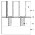
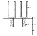
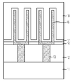
도 1a 내지 도 1c는 종래 기술에 따른 실린더형 캐패시터의 제조방법을 설명하기 위한 공정 단면도,1A to 1C are cross-sectional views illustrating a method of manufacturing a cylindrical capacitor according to the prior art;
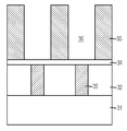
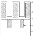
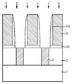
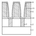
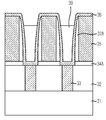
도 2a 내지 도 2i는 본 발명의 바람직한 실시예에 따른 반도체 소자의 제조방법을 설명하기 위한 공정 단면도.2A to 2I are cross-sectional views illustrating a method of manufacturing a semiconductor device in accordance with a preferred embodiment of the present invention.
* 도면의 주요 부분에 대한 부호의 설명* Explanation of symbols for the main parts of the drawings
31 : 반도체 기판 32 : 절연층31
33 : 스토리지노드콘택플러그 34 : 식각방지막33: storage node contact plug 34: etching prevention film
35 : 상부전극용 제1도전층 36 : 스토리지노드홀35: first conductive layer for the upper electrode 36: storage node hole
37 : 제1유전막 38 : 하부전극용 도전층37: first dielectric film 38: conductive layer for lower electrode
39 : 감광막 40 : 제2유전막39: photosensitive film 40: second dielectric film
41 : 상부전극용 제2도전층41: second conductive layer for the upper electrode
101 : 유전막 102 : 상부전극101
본 발명은 반도체 제조 기술에 관한 것으로, 특히 반도체 소자의 캐패시터 제조방법에 관한 것이다.BACKGROUND OF THE INVENTION 1. Field of the Invention The present invention relates to semiconductor manufacturing technology, and more particularly, to a method for manufacturing a capacitor of a semiconductor device.
반도체 소자가 고집적화 되면서 메모리 셀(Memory Cell)면적은 빠른 속도로 감소하고 있다. 그러나, 신뢰성 있는 소자 동작을 위해서 메모리 셀당 요구되는 정전용량(Capacitance)은 30fF/cell로 매우 높고, 작아진 메모리 셀 면적에서 요구되는 정전용량을 맞추기 위해 캐패시터 구조를 기존의 콘케이브형(Concave Type) 캐패시터 구조에서 실린더형(Cylinder Type) 캐패시터 구조로 대체하는 방법이 제안되고 있다.As semiconductor devices are highly integrated, memory cell areas are rapidly decreasing. However, the capacitance required per memory cell for reliable device operation is very high at 30fF / cell, and the capacitor structure can be used in order to meet the required capacitance in a smaller memory cell area. A method of replacing a capacitor structure with a cylinder type capacitor structure has been proposed.
실린더형 캐패시터는 하부전극(Bottom electrode meterial)의 안밖을 모두 캐패시터로 사용할 수 있어서 캐패시터 면적을 캐패시터의 내부뿐만 아니라 외부까지 확장시킴으로써 보다 큰 정전용량 확보 및 소자의 신뢰성을 확보할 수 있는 효과가 있다.The cylindrical capacitor can use both inside and outside of the bottom electrode meterial as a capacitor, thereby extending the capacitor area to the outside as well as the inside of the capacitor, thereby ensuring greater capacitance and device reliability.
도 1a 내지 도 1c는 종래 기술에 따른 실린더형 캐패시터의 제조방법을 설명하기 위한 공정 단면도이다.1A to 1C are cross-sectional views illustrating a method of manufacturing a cylindrical capacitor according to the prior art.
도 1a에 도시된 바와 같이, 소정공정이 완료된 반도체 기판(11) 상부에 절연층(12)을 형성한다. 여기서, 반도체 기판(11)은 반도체 기판 상부에 게이트패턴 및 비트라인의 소정공정이 완료된 것이다. 여기서, 절연층(12)은 산화막으로 형성한다.As shown in FIG. 1A, an
이어서, 절연층(12)을 선택적으로 식각하여 스토리지노드콘택홀을 형성하고 스토리지노드콘택홀에 도전물질을 매립하여 스토리지노드콘택플러그(13)를 형성한다.Subsequently, the
이어서, 식각방지막(14)과 희생층(15)을 순차로 형성하고, 희생층(15) 및 식각방지막(14)을 선택적으로 식각하여 하부전극을 위한 오픈부를 형성한 후, 오픈부의 표면을 따라 도전층을 형성하고 도전층을 분리하여 하부전극(16)을 형성한다. 여기서, 식각방지막(14)은 절연층 및 희생층(12, 15)과 식각선택비가 다른 물질로 형성하되 질화막으로 형성하고, 희생층(15)은 절연층(12)과 동일한 물질로 형성하되 산화막으로 형성한다.Subsequently, the
도 1b에 도시된 바와 같이, 딥아웃(Dip Out)을 실시하여 희생층(15)을 제거하여 실린더형 하부전극(16)을 형성한다.As shown in FIG. 1B, the
도 1c에 도시된 바와 같이, 하부전극(16) 상에 유전막(17)과 상부전극(18)을 순차로 적층하여 실린더형 캐패시터를 형성한다.As shown in FIG. 1C, a
위와 같이, 종래 기술은 희생층(15)을 선택적으로 식각하여 하부전극을 위한 오픈부를 형성한 후, 하부전극(16)을 형성하고 희생층(15)을 딥아웃으로 제거하여 실린더형 하부전극(16)을 형성한다. 이때, 희생층(15)을 제거하는 딥아웃 공정은 실린더형 캐패시터를 형성하기 위한 필수적인 공정이다.As described above, in the prior art, the
그러나, 종래 기술은 희생층(15)을 습식딥아웃으로 제거하는 공정에서 산화막질의 희생층(15)을 녹이고 딥아웃을 실시한 용액이 마를때 하부전극(16)이 기울어져서 이웃하는 하부전극(16)과 맞닿는 리닝(leaning)현상이 발생한다.However, in the prior art, in the process of removing the
상기와 같은, 리닝현상은 반도체 소자의 디자인 룰이 작아짐으로 인해 패턴 사이의 거리는 좁아지고, 하부전극(16)의 높이는 같거나 더 늘어나면서 더 심해지는 문제점이 있다. 특히, 상기와 같은 리닝현상은 어드레스(Address)에 따른 전하 저장이 되지 않는 불량이 발생하는 문제점이 있다. As described above, the lining phenomenon has a problem in that the distance between the patterns is narrowed due to the smaller design rules of the semiconductor device, and the height of the
또한, 웨이퍼 측면에서 보면 웨이퍼의 모서리(Edge)쪽에서 하부전극을 위한 오픈부를 정의하는 감광막패턴 형성을 위해 감광막의 노광 및 현상 공정에서 포커스가 맞지 않아 감광막패턴이 잘 형성되지 않고, 이로 인해 하부전극을 위한 오픈부가 작게 형성되거나 오픈불량(Not Open)의 문제가 발생한다. 이는 후속 하부전극 형성 후 희생층을 딥아웃으로 제거하는 공정에서 패턴 리프팅(Pattern Lifting)을 발생시킨다.In addition, from the side of the wafer, in order to form a photoresist pattern defining an open portion for the lower electrode at the edge of the wafer, the photoresist pattern is not formed well because the photoresist pattern is not in focus during the exposure and development of the photoresist. The open part is formed small or a problem of Not Open occurs. This causes pattern lifting in the process of removing the sacrificial layer by deep out after the formation of the subsequent lower electrode.
위와 같은, 패턴 리프팅을 방지하기 위해서는 웨이퍼 모서리쪽에 형성된 다이(Die)의 크기에 맞추어 따로 감광막패턴을 형성해야하는 추가공정을 필요로 하다. 이러한 추가공정은 생산성하락과 공정단가를 증가시키는 문제점이 있다.In order to prevent the pattern lifting as described above, an additional process of forming a photoresist pattern separately according to the size of a die formed on the edge of the wafer is required. This additional process has the problem of lowering productivity and increasing process cost.
본 발명은 상기한 종래 기술의 문제점을 해결하기 위해 제안된 것으로, 실린더형 캐패시터를 형성하기 위한 필수 공정인 딥아웃 공정에서 리닝현상이 발생하는 문제점을 방지하고, 생산성향상 및 공정단가를 확보하는 반도체 소자의 제조방법을 제공하는데 그 목적이 있다.The present invention has been proposed to solve the above problems of the prior art, a semiconductor that prevents the problem of the occurrence of the lining phenomenon in the deep-out process, which is an essential process for forming a cylindrical capacitor, and improves the productivity and process cost Its purpose is to provide a method for manufacturing a device.
본 발명에 의한 반도체 소자의 제조방법은 기판 상부에 하부전극을 위한 오픈부를 정의하는 제1도전층을 형성하는 단계, 상기 오픈부의 측벽에 제1유전막을 형성하는 단계, 상기 제1도전층보다 낮은 높이로 상기 오픈부의 표면을 따라 제2도전층을 형성하는 단계, 상기 오픈부의 내부표면을 따라 상기 제1유전막의 상부와 연결되는 제2유전막을 형성하는 단계, 상기 제2유전막 상에 상기 스토리지노드홀을 매립하도록 제3도전층을 형성하는 단계를 포함하는 것을 특징으로 한다.A method of manufacturing a semiconductor device according to the present invention includes forming a first conductive layer defining an open portion for a lower electrode on a substrate, forming a first dielectric layer on sidewalls of the open portion, and lowering the first conductive layer. Forming a second conductive layer along the surface of the open portion at a height, forming a second dielectric layer connected to an upper portion of the first dielectric layer along an inner surface of the open portion, and forming the storage node on the second dielectric layer And forming a third conductive layer to fill the hole.
특히, 제1도전층과 제3도전층은 캐패시터의 상부전극으로 사용하고, 폴리실리콘으로 형성하는 것을 특징으로 한다. 또한, 제2도전층은 캐패시터의 하부전극으로 사용하고, 폴리실리콘 또는 티타늄질화막으로 형성하는 것을 특징으로 한다.In particular, the first conductive layer and the third conductive layer are used as the upper electrode of the capacitor, characterized in that formed of polysilicon. In addition, the second conductive layer is used as a lower electrode of the capacitor, characterized in that formed of polysilicon or titanium nitride film.
이하, 본 발명이 속하는 기술 분야에서 통상의 지식을 가진 자가 본 발명의 기술적 사상을 용이하게 실시할 수 있을 정도로 상세히 설명하기 위하여, 본 발명의 가장 바람직한 실시예를 첨부 도면을 참조하여 설명하기로 한다.Hereinafter, the most preferred embodiments of the present invention will be described in detail with reference to the accompanying drawings so that those skilled in the art can easily implement the technical idea of the present invention. .
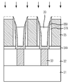
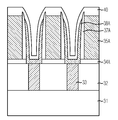
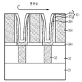
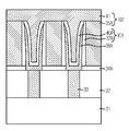
도 2a 내지 도 2i는 본 발명의 바람직한 실시예에 따른 반도체 소자의 제조방법을 설명하기 위한 공정 단면도이다.2A to 2I are cross-sectional views illustrating a method of manufacturing a semiconductor device in accordance with a preferred embodiment of the present invention.
도 2a에 도시된 바와 같이, 소정공정이 완료된 반도체 기판(31) 상부에 절연층(32)을 형성한다. 여기서, 반도체 기판(31)은 소자분리막과 웰(well)이 포함된 반도체 기판 상부에 게이트패턴 및 비트라인의 소정공정이 완료된 것이다. 또한, 절연층(32)은 반도체 기판(31)과 후속 캐패시터간의 층간절연막 역할을 하기 위한 것으로, 산화막으로 형성한다.As shown in FIG. 2A, an
이어서, 절연층(32)을 선택적으로 식각하여 스토리지노드콘택홀을 형성하고, 스토리지노드콘택홀을 매립하는 스토리지노드콘택플러그(33)를 형성한다. 여기서, 스토리지노드콘택플러그(33)는 스토리지노드콘택홀에 도전물질을 매립하고 평탄화하여 형성하는데, 도전물질로는 예컨대 폴리실리콘으로 형성한다. 또한, 평탄화는 화학적기계적연마(Chemical Mechanical Polishing;CMP) 또는 전면식각(Etch Back)으로 실시한다.Subsequently, the
이어서, 스토리지노드콘택플러그(33)를 포함하는 결과물의 전면에 식각방지막(34)을 형성한다. 여기서, 식각방지막(34)은 후속 하부전극을 위한 오픈부를 형성하는 공정에서 식각에 의해 절연층(32) 및 스토리지노드콘택플러그(33)가 손상되는 것을 방지하기 위한 식각방지막 역할을 하기 위한 것으로, 예컨대 질화막으로 형성한다.Subsequently, an
이어서, 식각방지막(34) 상에 하부전극을 위한 오픈부(36)를 정의하는 상부전극용 제1도전층(35)을 형성한다. 여기서, 상부전극용 제1도전층(35)은 후속공정에서 캐패시터의 상부전극으로 사용하기 위한 것으로, 예컨대 상부전극용 제1도전층(35)은 폴리실리콘으로 형성한다.Subsequently, the first
이는, 종래에 산화막질의 희생층을 형성한 후 딥아웃으로 제거하는 공정에서 딥아웃에 사용된 용액에 의한 하부전극의 리닝현상을 방지하기 위해 희생층 대신 상부전극으로 사용될 상부전극용 제1도전층(35)을 미리 형성하는 것이다. The first conductive layer for the upper electrode, which is to be used as the upper electrode instead of the sacrificial layer, in order to prevent the lowering of the lower electrode due to the solution used for the dipout in the process of forming the sacrificial layer of the oxide film and then removing it by the dipout. 35 is formed in advance.
또한, 상부전극용 제1도전층(35)은 예정된 캐패시터의 높이 또는 후속 평탄화공정에서 손실되는 부분을 감안하여 예정된 캐패시터의 높이보다 높게 형성한다. 예컨대, 예정된 캐패시터의 높이가 10000Å이고 후속 평탄화공정에서 상부전극용 제1도전층(35)이 2000Å만큼의 손실이 예상될 경우 상부전극용 제1도전층(35)은 12000Å으로 형성한다.In addition, the first
위와 같이, 오픈부(36)를 정의하는 상부전극용 제1도전층(35)을 형성하는 공정은, 식각방지막(34) 상에 상부전극용 제1도전층(35)을 형성하고, 상부전극용 제1도전층(35) 상에 감광막을 코팅한 후 노광 및 현상으로 하부전극을 위한 오픈부예정지역을 정의하도록 패터닝한다. 이어서, 패터닝된 감광막을 식각마스크로 상기 상부전극용 제1도전층(35)을 식각하여 하부전극을 위한 오픈부(36)를 형성한다. 이어서, 감광막을 산소스트립공정으로 제거한다.As described above, in the process of forming the first
상부전극용 제1도전층(35)의 식각이 완료되는 시점에서 상부전극용 제1도전층(35)과의 식각선택비로 식각방지막(34)은 식각되지 않고 그대로 잔류한다.When the etching of the first
도 2b에 도시된 바와 같이, 상부전극용 제1도전층(35) 상에 제1유전막(37)을 형성한다. 여기서, 제1유전막(37)은 후속 제2유전막과 연결되어 캐패시터의 유전막으로 사용하기 위한 것으로, 단층 또는 다층의 유전물질로 형성한다.As shown in FIG. 2B, the
도 2c에 도시된 바와 같이, 제1유전막(37)을 식각하여 오픈부(36)의 측벽에만 제1유전막(37A)을 잔류시킨다. 여기서, 제1유전막(37A)의 식각은 전면식각으로 실시하되, 상부전극용 제1도전층(35)의 상부 및 오픈부(36)의 바닥에 형성된 제1유전막(37A)을 제거하여, 상부전극용 제1도전층(35)과 동일한 높이로 오픈부(36)의 측벽에만 제1유전막(37A)을 잔류시킨다. As shown in FIG. 2C, the
또한, 제1유전막(37A)의 식각과 동시에 오픈부(36) 하부의 식각방지막(34A) 도 함께 식각하여 하부 스토리지노드콘택플러그(33)의 표면을 노출시킨다.In addition, at the same time as the etching of the first
도 2d에 도시된 바와 같이, 제1유전막(37A)을 포함하는 전면을 따라 하부전극용 도전층(38)을 형성한다. 여기서, 하부전극용 도전층(38)은 캐패시터의 하부전극역할을 하기 위한 것으로, 예컨대 폴리실리콘 또는 금속물질로 형성하고 특히, 금속물질은 티타늄질화막으로 형성한다. As shown in FIG. 2D, the
특히, 티타늄질화막과 같은 금속물질로 형성할 경우 폴리실리콘으로 형성한 상부전극용 제1도전층(35)과 식각선택비를 확보할 수 있어서 후속 전면식각 공정시 상부전극용 제1도전층(35)의 손실 및 두께조절을 더 용이하게 할 수 있는 장점이 있다.In particular, when formed of a metal material such as a titanium nitride film, the first
도 2e에 도시된 바와 같이, 오픈부(36)의 내부에 상부전극용 제1도전층(35)보다 낮은 높이로 감광막(39)을 형성한다. 여기서, 감광막(39)은 후속 하부전극용 도전층(38) 식각시 오픈부(36) 바닥의 하부전극용 도전층(38)을 보호하는 보호층 역할을 하기 위한 것이다. As shown in FIG. 2E, the
특히, 감광막(39)을 상부전극용 제1도전층(35)보다 낮은 높이로 형성하기 위해서 먼저 오픈부(36)의 내부를 채우도록 감광막(39)을 코팅하고 상부전극용 제1도전층(35)보다 낮은 높이가 되도록 노광 및 현상을 실시한다. In particular, in order to form the
도 2f에 도시된 바와 같이, 하부전극용 도전층(38A)을 제1유전막(37A) 및 상부전극용 제1도전층(35)의 높이보다 낮게 식각한다. 여기서, 하부전극용 도전층(38A)의 식각은 전면식각을 실시한다.As shown in FIG. 2F, the lower electrode
특히, 하부전극용 도전층(38A)을 전면식각하는 것과 동시에 상부전극용 제1도전층(35A)도 일정높이 식각하여 상부전극용 제1도전층(35A) 상부로 제1유전막(37A)을 돌출시킨다. 그러나, 상부전극용 제1도전층(35A)은 하부전극용 도전층(38A)에 비해 식각되는 두께가 작다. 이는 상부전극용 제1도전층(35A) 상에 형성된 하부전극용 도전층(38A)의 두께까지 고려되기 때문이다. 또한, 하부전극용 도전층(38A)을 대신하여 금속물질을 사용할 경우 폴리실리콘과 금속물질간의 식각선택비를 이용하여 식각두께를 조절할 수 있다.In particular, the lower surface
이때, 오픈부(36) 바닥의 하부전극용 도전층(38A)은 오픈부(36) 내부에 형성된 감광막(39)으로 보호되어 식각되지 않고, 또한 전면식각시 감광막(39)이 일부 소실된다고 해도 오픈부(36) 내부에 여전히 잔류하여 바닥의 하부전극용 도전층(38A)을 보호하기 때문에 전면식각시에 큰 영향을 미치지 않는다.At this time, the lower electrode
위와 같이, 하부전극용 폴리실리콘층(38A)에 전면식각을 실시함으로써 스토리지노드콘택플러그(33)와 연결되는 하부전극(38A)이 형성된다. 즉, 희생층을 형성하지 않았기 때문에 딥아웃공정 없이 실린더형 하부전극(38A)을 형성할 수 있다.As described above, the
도 2g에 도시된 바와 같이, 오픈부(36) 내부의 감광막(39)을 제거한다. 여기서, 감광막(39)은 건식식각으로 제거하되 바람직하게는 산소스트립으로 제거한다.As shown in FIG. 2G, the
이어서, 하부전극(38A)을 포함하는 전면을 따라 제2유전막(40)을 형성한다. 여기서, 제2유전막(40)은 제1유전막(37A)과 함께 캐패시터의 유전막역할을 하기 위한 것으로, 제1유전막(37A)과 동일한 물질로 형성하되 단층 또는 다층의 유전물질로 형성한다.Next, a
도 2h에 도시된 바와 같이, 상부전극용 제1도전층(35A) 상부에 형성된 제2유 전막(40)과 상부전극용 제1도전층(35A)의 상부로 돌출된 제1유전막(37A)을 식각한다. 여기서, 제1 및 제2유전막(37A, 40)의 식각은 평탄화공정으로 실시한다. 특히, 평탄화공정은 상부전극용 제1도전층(35A)의 표면이 드러나는 타겟으로 실시하되, 예컨대 화학적기계적연마(CMP) 또는 전면식각(Etch back)으로 실시한다.As shown in FIG. 2H, the
위와 같이, 평탄화공정을 실시함으로써 상부전극용 제1도전층(35A)의 상부로 돌출된 부분이 제거된 제1유전막(37B)의 상부와 하부전극(38A)상에 오픈부(36)의 내부표면을 따라 형성된 제2유전막(40A)이 연결되어 캐패시터의 유전막(101)이 형성된다. As described above, the inside of the
도 2i에 도시된 바와 같이, 유전막(101) 상에 오픈부(36)을 채우도록 상부전극용 제2도전층(41)을 형성한다. 여기서, 상부전극용 제2도전층(41)은 하부의 상부전극용 제1도전층(35A)과 연결되어 캐패시터의 상부전극(102) 역할을 하기 위한 것으로, 예컨대 폴리실리콘으로 형성한다.As shown in FIG. 2I, the second
상기한 본 발명은, 하부전극을 위한 오픈부(36)를 정의하는 상부전극용 제1도전층(35)을 형성한 후 증착과 식각 및 평탄화공정을 차례로 실시하여 습식딥아웃 없이 실린더형 캐패시터를 함으로써, 딥아웃으로 인해 발생하는 하부전극의 리닝현상을 근본적으로 방지하면서 종래의 실린더형 캐패시터와 동일한 형태의 구현이 가능한 장점이 있다. In the present invention described above, after forming the first
또한, 오픈부 형성시 웨이퍼의 모서리에서 발생한 패턴불량으로 인해 희생층을 제거하는 딥아웃공정을 실시하지 않음으로써 패턴 리프팅(Pattern lifting)을 방지할 수 있을 뿐만 아니라, 패턴 리프팅을 해결하기 위해 실시된 감광막패턴 형성의 추가공정을 진행하지 않음으로써 공정마진을 확보하여 생산성향상 및 공정단가를 확보할 수 있는 장점이 있다.In addition, the pattern lifting may not only be prevented by removing the deep-out process of removing the sacrificial layer due to the pattern defect generated at the edge of the wafer when the open portion is formed, but also to solve the pattern lifting. By not proceeding with the additional process of forming the photoresist pattern, it is possible to secure process margins and to increase productivity and process costs.
또한, 본 실시예는 상부전극용 제1 및 제2도전층으로 폴리실리콘을, 하부전극용 도전층으로 폴리실리콘 또는 티타늄질화막을 사용하였지만 본 발명의 기술적 사상은 폴리실리콘 또는 티타늄질화막 외에 상부전극 및 하부전극을 위한 도전물질에 모두 응용될 수 있다.In addition, in the present embodiment, polysilicon is used as the first and second conductive layers for the upper electrode, and polysilicon or titanium nitride is used as the conductive layer for the lower electrode. It can be applied to all conductive materials for the lower electrode.
이렇듯, 본 발명의 기술 사상은 상기 바람직한 실시예에 따라 구체적으로 기술되었으나, 상기한 실시예는 그 설명을 위한 것이며 그 제한을 위한 것이 아님을 주의하여야 한다. 또한, 본 발명의 기술 분야의 통상의 전문가라면 본 발명의 기술 사상의 범위 내에서 다양한 실시예가 가능함을 이해할 수 있을 것이다.As such, although the technical idea of the present invention has been described in detail according to the above-described preferred embodiment, it should be noted that the above-described embodiment is for the purpose of description and not of limitation. In addition, those skilled in the art will understand that various embodiments are possible within the scope of the technical idea of the present invention.
상술한 본 발명은 딥아웃공정으로 인해 발생하는 리닝현상을 방지하면서도 실린더형 캐패시터와 동일한 형태로 구현할 수 있는 효과가 있다.The present invention described above has the effect that can be implemented in the same form as the cylindrical capacitor while preventing the lining phenomenon caused by the dipout process.
또한, 딥아웃 공정시 웨이퍼 모서리에서 발생하는 패턴 리프팅을 방지할 수 있어서 추가공정을 실시하지 않음으로써 공정마진을 확보하여 생산성향상 및 공정단가를 확보할 수 있는 효과가 있다.In addition, the pattern lifting occurring at the edge of the wafer during the deep-out process can be prevented, so that the process margin is secured by not performing an additional process, thereby improving productivity and securing a process cost.
Claims (9)
Priority Applications (1)
| Application Number | Priority Date | Filing Date | Title |
|---|---|---|---|
| KR1020060100792A KR100875649B1 (en) | 2006-10-17 | 2006-10-17 | Semiconductor device manufacturing method |
Applications Claiming Priority (1)
| Application Number | Priority Date | Filing Date | Title |
|---|---|---|---|
| KR1020060100792A KR100875649B1 (en) | 2006-10-17 | 2006-10-17 | Semiconductor device manufacturing method |
Publications (2)
| Publication Number | Publication Date |
|---|---|
| KR20080034615A KR20080034615A (en) | 2008-04-22 |
| KR100875649B1 true KR100875649B1 (en) | 2008-12-26 |
Family
ID=39573944
Family Applications (1)
| Application Number | Title | Priority Date | Filing Date |
|---|---|---|---|
| KR1020060100792A Expired - Fee Related KR100875649B1 (en) | 2006-10-17 | 2006-10-17 | Semiconductor device manufacturing method |
Country Status (1)
| Country | Link |
|---|---|
| KR (1) | KR100875649B1 (en) |
-
2006
- 2006-10-17 KR KR1020060100792A patent/KR100875649B1/en not_active Expired - Fee Related
Also Published As
| Publication number | Publication date |
|---|---|
| KR20080034615A (en) | 2008-04-22 |
Similar Documents
| Publication | Publication Date | Title |
|---|---|---|
| US12069859B2 (en) | Semiconductor structure with high inter-layer dielectric layer and manufacturing method thereof | |
| CN112864153B (en) | Semiconductor structure and preparation method thereof | |
| JP5062969B2 (en) | Method for forming landing plug contact of semiconductor device | |
| KR100589078B1 (en) | Capacitor manufacturing method and DRAM device manufacturing method employing the same | |
| KR100875649B1 (en) | Semiconductor device manufacturing method | |
| KR100587636B1 (en) | Capacitor Formation Method of Semiconductor Device | |
| KR20090022381A (en) | Method for manufacturing contact plug of semiconductor device | |
| KR100607651B1 (en) | Manufacturing method of capacitor | |
| KR100702112B1 (en) | Manufacturing method of storage node electrode of semiconductor memory device | |
| KR100345665B1 (en) | Method of fabricating semiconductor memory device | |
| KR100557956B1 (en) | Capacitor Formation Method of Semiconductor Device | |
| US7482257B2 (en) | Method for forming metal contact in semiconductor device | |
| KR20080100548A (en) | Contact formation method of semiconductor device | |
| KR100906641B1 (en) | Method for manufacturing a semiconductor device having a landing plug | |
| KR101061171B1 (en) | Method of manufacturing semiconductor device | |
| KR0138292B1 (en) | Contact hole formation method of semiconductor device | |
| KR100955263B1 (en) | Method of manufacturing semiconductor device | |
| KR101173478B1 (en) | Method for fabricating semiconductor device | |
| KR20040022043A (en) | Method of forming Capacitor in Semiconductor devices | |
| KR101116286B1 (en) | Method for fabricating buried gate with semiconductor device | |
| KR100844939B1 (en) | Method of manufacturing semiconductor device with gate line of fine line width | |
| KR100866701B1 (en) | Manufacturing Method of Semiconductor Device | |
| KR20010076525A (en) | A Method of Forming Cylinder Type Storage Node for Memory Devices | |
| KR20090022802A (en) | Manufacturing method of semiconductor device | |
| KR20090022378A (en) | Manufacturing method of semiconductor device |
Legal Events
| Date | Code | Title | Description |
|---|---|---|---|
| A201 | Request for examination | ||
| PA0109 | Patent application |
St.27 status event code: A-0-1-A10-A12-nap-PA0109 |
|
| PA0201 | Request for examination |
St.27 status event code: A-1-2-D10-D11-exm-PA0201 |
|
| D13-X000 | Search requested |
St.27 status event code: A-1-2-D10-D13-srh-X000 |
|
| D14-X000 | Search report completed |
St.27 status event code: A-1-2-D10-D14-srh-X000 |
|
| E902 | Notification of reason for refusal | ||
| PE0902 | Notice of grounds for rejection |
St.27 status event code: A-1-2-D10-D21-exm-PE0902 |
|
| E902 | Notification of reason for refusal | ||
| PE0902 | Notice of grounds for rejection |
St.27 status event code: A-1-2-D10-D21-exm-PE0902 |
|
| AMND | Amendment | ||
| P11-X000 | Amendment of application requested |
St.27 status event code: A-2-2-P10-P11-nap-X000 |
|
| P13-X000 | Application amended |
St.27 status event code: A-2-2-P10-P13-nap-X000 |
|
| PG1501 | Laying open of application |
St.27 status event code: A-1-1-Q10-Q12-nap-PG1501 |
|
| E601 | Decision to refuse application | ||
| PE0601 | Decision on rejection of patent |
St.27 status event code: N-2-6-B10-B15-exm-PE0601 |
|
| J201 | Request for trial against refusal decision | ||
| PJ0201 | Trial against decision of rejection |
St.27 status event code: A-3-3-V10-V11-apl-PJ0201 |
|
| AMND | Amendment | ||
| E13-X000 | Pre-grant limitation requested |
St.27 status event code: A-2-3-E10-E13-lim-X000 |
|
| P11-X000 | Amendment of application requested |
St.27 status event code: A-2-2-P10-P11-nap-X000 |
|
| P13-X000 | Application amended |
St.27 status event code: A-2-2-P10-P13-nap-X000 |
|
| PB0901 | Examination by re-examination before a trial |
St.27 status event code: A-6-3-E10-E12-rex-PB0901 |
|
| B701 | Decision to grant | ||
| PB0701 | Decision of registration after re-examination before a trial |
St.27 status event code: A-3-4-F10-F13-rex-PB0701 |
|
| GRNT | Written decision to grant | ||
| PR0701 | Registration of establishment |
St.27 status event code: A-2-4-F10-F11-exm-PR0701 |
|
| PR1002 | Payment of registration fee |
St.27 status event code: A-2-2-U10-U11-oth-PR1002 Fee payment year number: 1 |
|
| PG1601 | Publication of registration |
St.27 status event code: A-4-4-Q10-Q13-nap-PG1601 |
|
| LAPS | Lapse due to unpaid annual fee | ||
| PC1903 | Unpaid annual fee |
St.27 status event code: A-4-4-U10-U13-oth-PC1903 Not in force date: 20111218 Payment event data comment text: Termination Category : DEFAULT_OF_REGISTRATION_FEE |
|
| PN2301 | Change of applicant |
St.27 status event code: A-5-5-R10-R13-asn-PN2301 St.27 status event code: A-5-5-R10-R11-asn-PN2301 |
|
| PC1903 | Unpaid annual fee |
St.27 status event code: N-4-6-H10-H13-oth-PC1903 Ip right cessation event data comment text: Termination Category : DEFAULT_OF_REGISTRATION_FEE Not in force date: 20111218 |
|
| PN2301 | Change of applicant |
St.27 status event code: A-5-5-R10-R13-asn-PN2301 St.27 status event code: A-5-5-R10-R11-asn-PN2301 |
|
| PN2301 | Change of applicant |
St.27 status event code: A-5-5-R10-R13-asn-PN2301 St.27 status event code: A-5-5-R10-R11-asn-PN2301 |
|
| P22-X000 | Classification modified |
St.27 status event code: A-4-4-P10-P22-nap-X000 |
|
| P22-X000 | Classification modified |
St.27 status event code: A-4-4-P10-P22-nap-X000 |
|
| P22-X000 | Classification modified |
St.27 status event code: A-4-4-P10-P22-nap-X000 |
|
| P22-X000 | Classification modified |
St.27 status event code: A-4-4-P10-P22-nap-X000 |