KR100843546B1 - Multi-chip Package Flash Memory Device and Its Status Signal Reading Method - Google Patents
Multi-chip Package Flash Memory Device and Its Status Signal Reading Method Download PDFInfo
- Publication number
- KR100843546B1 KR100843546B1 KR1020060115387A KR20060115387A KR100843546B1 KR 100843546 B1 KR100843546 B1 KR 100843546B1 KR 1020060115387 A KR1020060115387 A KR 1020060115387A KR 20060115387 A KR20060115387 A KR 20060115387A KR 100843546 B1 KR100843546 B1 KR 100843546B1
- Authority
- KR
- South Korea
- Prior art keywords
- output
- input
- memory chips
- chip
- state data
- Prior art date
- Legal status (The legal status is an assumption and is not a legal conclusion. Google has not performed a legal analysis and makes no representation as to the accuracy of the status listed.)
- Active
Links
Images


Classifications
-
- G—PHYSICS
- G06—COMPUTING OR CALCULATING; COUNTING
- G06F—ELECTRIC DIGITAL DATA PROCESSING
- G06F11/00—Error detection; Error correction; Monitoring
- G06F11/22—Detection or location of defective computer hardware by testing during standby operation or during idle time, e.g. start-up testing
- G06F11/26—Functional testing
- G06F11/263—Generation of test inputs, e.g. test vectors, patterns or sequences ; with adaptation of the tested hardware for testability with external testers
-
- G—PHYSICS
- G06—COMPUTING OR CALCULATING; COUNTING
- G06F—ELECTRIC DIGITAL DATA PROCESSING
- G06F13/00—Interconnection of, or transfer of information or other signals between, memories, input/output devices or central processing units
- G06F13/14—Handling requests for interconnection or transfer
- G06F13/16—Handling requests for interconnection or transfer for access to memory bus
- G06F13/1668—Details of memory controller
- G06F13/1684—Details of memory controller using multiple buses
-
- G—PHYSICS
- G06—COMPUTING OR CALCULATING; COUNTING
- G06F—ELECTRIC DIGITAL DATA PROCESSING
- G06F11/00—Error detection; Error correction; Monitoring
-
- G—PHYSICS
- G06—COMPUTING OR CALCULATING; COUNTING
- G06F—ELECTRIC DIGITAL DATA PROCESSING
- G06F11/00—Error detection; Error correction; Monitoring
- G06F11/22—Detection or location of defective computer hardware by testing during standby operation or during idle time, e.g. start-up testing
- G06F11/26—Functional testing
-
- G—PHYSICS
- G06—COMPUTING OR CALCULATING; COUNTING
- G06F—ELECTRIC DIGITAL DATA PROCESSING
- G06F11/00—Error detection; Error correction; Monitoring
- G06F11/30—Monitoring
- G06F11/34—Recording or statistical evaluation of computer activity, e.g. of down time, of input/output operation ; Recording or statistical evaluation of user activity, e.g. usability assessment
Landscapes
- Engineering & Computer Science (AREA)
- Theoretical Computer Science (AREA)
- General Engineering & Computer Science (AREA)
- Physics & Mathematics (AREA)
- General Physics & Mathematics (AREA)
- Quality & Reliability (AREA)
- Computer Hardware Design (AREA)
- Read Only Memory (AREA)
Abstract
본 발명에 따른 복수의 메모리 칩들을 포함하는 멀티 칩 메모리 장치의 상태 데이터 출력 방법은 상기 복수의 메모리 칩들로 상기 상태 데이터의 출력을 지시하는 명령어를 제공하는 단계; 그리고 상기 복수의 메모리 칩들 각각의 상태 데이터를 상기 멀티 칩 메모리 장치의 서로 다른 입출력 라인들을 통하여 제공받는 단계를 포함한다. 상술한 멀티 칩 메모리 장치의 상태 데이터의 출력 방법에 따르면, 멀티 칩 메모리 장치의 상태 데이터를 제공받기 위한 대기시간을 줄일 수 있어 동작 속도를 향상시킬 수 있다.
In accordance with another aspect of the present invention, there is provided a method of outputting state data of a multi-chip memory device including a plurality of memory chips; And receiving state data of each of the plurality of memory chips through different input / output lines of the multi-chip memory device. According to the method of outputting the state data of the multi-chip memory device, the waiting time for receiving the state data of the multi-chip memory device can be reduced, thereby improving the operation speed.
Description
도 1는 일반적인 멀티 칩 플래시 메모리 장치의 레디/비지 신호의 출력 방식을 간략히 보여주는 타이밍도;1 is a timing diagram briefly illustrating an output scheme of a ready / busy signal of a general multi-chip flash memory device;
도 2는 본 발명의 멀티 칩 플래시 메모리 장치의 구성을 간략히 보여주는 블록도;2 is a block diagram schematically showing the configuration of a multi-chip flash memory device of the present invention;
도 3은 상술한 도 2의 메모리 칩 각각의 내부 구성을 간략히 보여주는 블록도;3 is a block diagram schematically illustrating an internal configuration of each of the memory chips of FIG. 2 described above;
도 4는 본 발명에 따른 멀티 칩 플래시 메모리 장치의 레디/비지 신호의 출력을 간략히 보여주는 타이밍도;4 is a timing diagram briefly showing an output of a ready / busy signal of a multi-chip flash memory device according to the present invention;
도 5는 도 2에 도시된 각 메모리 칩들에 대한 레디/비지 신호의 할당 방식을 예시적으로 보여주는 표;5 is a table exemplarily illustrating a method of allocating a ready / busy signal for each of the memory chips illustrated in FIG. 2;
도 6은 본 발명에 따른 멀티 칩 플래시 메모리 장치의 인터리브 프로그램 동작을 간략히 보여주는 타이밍도;6 is a timing diagram briefly showing an interleaved program operation of a multichip flash memory device according to the present invention;
도 7은 본 발명에 따른 멀티 칩 플래시 메모리 장치를 장착하는 시스템을 간략히 보여주는 블록도.7 is a block diagram schematically illustrating a system for mounting a multi-chip flash memory device according to the present invention.
* 도면의 주요 부분에 대한 부호 설명 *Explanation of symbols on the main parts of the drawings
10 : 멀티 칩 플래시 메모리10: multi-chip flash memory
20, 30, 40 : 메모리 칩 50 : 입출력 라인20, 30, 40: memory chip 50: input / output line
60 : 메모리 제어기 100 : 셀 어레이60: memory controller 100: cell array
110 : 출력 버퍼 120 : 입력 버퍼110: output buffer 120: input buffer
130 : 어드레스 레지스터 140 : 명령어 레지스터130: address register 140: instruction register
150 : 제어부 160 : RnB 핀 지정 블록150: control unit 160: RnB pin assignment block
170 : 디코더 210 : 플래시 메모리170: decoder 210: flash memory
220 : 제어기 230 : 중앙처리장치220: controller 230: central processing unit
240 : 램 250 : 입력 키240: RAM 250: Enter key
260 : 디스플레이 270 : 시스템 버스260: display 270: system bus
본 발명은 플래시 메모리 장치에 관한 것으로, 좀 더 구체적으로는 멀티 칩 플래시 메모리 장치 및 그것의 상태 신호 출력 방법에 관한 것이다. The present invention relates to a flash memory device, and more particularly to a multi-chip flash memory device and its status signal output method.
최근, 불 휘발성 메모리의 응용들이 MP3 플레이어, PMP, 휴대전화, 노트북 컴퓨터, PDA, 등과 같은 모바일 기기들에 급속히 확산되고 있다. 그러한 모바일 기기들은 다양한 기능들(예를 들면, 동영상 재생 기능)을 제공하기 위해서 점차 대용량의 저장 장치들을 필요로 하고 있다. 그러한 요구를 충족하기 위한 다양한 노력들이 행해져 오고 있다. 그러한 노력들 중 하나로서 패키지 내에 복수의 메모리 장 치를 구비하는 멀티 칩 패키지 스킴이 제안되어 있다. 멀티 칩 패키지 방식은 같은 종류의 메모리 칩들을 적층(Stack)함으로써 메모리의 용량 대비 패키지의 면적을 획기적으로 감소시킬 수 있다. 일반적으로 멀티 칩 플래시 메모리 장치에 포함되는 칩들 각각은 입출력 버스(I/O Bus) 및 제어 핀들을 공유한다. 그러나 각각의 메모리 칩들은 독립적으로 프로그램 동작이나 소거 동작을 수행할 수 있다. 이러한 각각의 메모리 칩들을 제어하고 외부 또는 호스트로 하나의 메모리 장치로 인식하도록 하기 위한 메모리 제어기가 제공되어야 한다. Recently, applications of nonvolatile memory are rapidly spreading to mobile devices such as MP3 players, PMPs, cellular phones, notebook computers, PDAs, and the like. Such mobile devices are increasingly in need of mass storage devices to provide various functions (eg, video playback functions). Various efforts have been made to meet that need. As one of such efforts, a multi-chip package scheme having a plurality of memory devices in a package has been proposed. In the multi-chip package method, by stacking memory chips of the same type, the area of the package may be significantly reduced compared to the capacity of the memory. In general, each of the chips included in the multi-chip flash memory device shares an I / O bus and control pins. However, each memory chip may independently perform a program operation or an erase operation. A memory controller should be provided for controlling each of these memory chips and for recognizing it as a memory device externally or to a host.
최근의 플래시 메모리 장치들은 칩 내부에 프로그램 및 소거 동작의 시퀀스 제어를 수행하는 메모리 제어기를 내장하고 있다. 이러한 플래시 메모리 장치에서는, 외부로부터 명령어와 프로그램 데이터가 입력되면, 데이터 쓰기 동작 및 그 후의 검증 동작을 포함하여 프로그램의 완료까지의 일련의 동작이 자동적으로 실행된다. 상술한 프로그램 및 소거 동작에 있어서, 동작 개시로부터 완료까지는 외부로는 레디/비지 신호(RnB)가 출력되어 액세스가 금지된다. 그러나 하나의 패키지 내에 복수의 플래시 메모리 칩이 내장되는 멀티 칩 플래시 메모리 장치에서는 모든 칩들이 동시에 프로그램 동작이나 소거 동작을 수행하지 않을 가능성이 크다. 따라서, 각각의 칩들은 칩들이 인식하는 고유한 명령어에 응답하여 서로 다른 시간에 레디/비지 신호를 외부의 호스트로 제공한다. 즉, 각각의 메모리 칩들의 레디/비지 신호들은 시분할적으로 제공되는 명령어에 의하여, 시분할적으로 출력된다. 일반적으로, 각각의 메모리 칩들은 레디/비지 신호(RnB)를 데이터의 입출력 수단으로 사용하는 입출력 핀(I/O 핀)으로 출력한다. Recent flash memory devices have built-in memory controllers that perform sequence control of program and erase operations within the chip. In such a flash memory device, when an instruction and program data are input from the outside, a series of operations up to completion of the program are automatically executed, including a data write operation and a subsequent verification operation. In the above-described program and erase operations, the ready / busy signal RnB is output from the start to the completion of the operation to the outside, thereby preventing access. However, in a multi-chip flash memory device in which a plurality of flash memory chips are embedded in one package, it is highly likely that all chips do not simultaneously perform a program operation or an erase operation. Thus, each chip provides a ready / busy signal to an external host at different times in response to a unique command that the chips recognize. That is, the ready / busy signals of the respective memory chips are output time-divisionally by a command provided by time-division. In general, each of the memory chips outputs a ready / busy signal RnB to an input / output pin (I / O pin) using the data input / output means.
도 1은 일반적인 멀티 칩 패키지 플래시 메모리 장치의 레디/비지 신호(RnB)의 출력 방식을 간략히 보여주는 타이밍도이다. 도 1을 참조하면, 일반적인 멀티 칩 플래시 메모리 장치는 상술한 설명과 같이 시분할 방식으로 레디/비지 신호(RnB)를 출력한다. 즉, 레디/비지 신호(RnB)를 출력하기 위한 명령어는 각각의 메모리 칩들로 서로 다른 시간에 각각 제공된다. FIG. 1 is a timing diagram briefly illustrating an output method of a ready / busy signal RnB of a general multi-chip package flash memory device. Referring to FIG. 1, a general multi-chip flash memory device outputs a ready / busy signal RnB in a time division manner as described above. That is, instructions for outputting the ready / busy signal RnB are provided to the respective memory chips at different times.
대용량 데이터를 저장하는 경우, 제공되는 데이터에 대해서 모든 칩들이 프로그램을 지속적으로 수행하는 인터리브(Interleave) 방식으로 동작할 수 있다. 이 경우, 호스트(Host) 또는 메모리 제어기(Momory Controller)는 메모리 칩들 각각의 프로그램 동작 여부를 확인하기 위해, 빈번하게 레디/비지 신호(RnB)를 각각의 칩들로 요청하게 된다. 시분할 방식으로 레디/비지 신호(RnB)를 출력하는 일반적인 멀티 칩 플래시 메모리 장치에서는 이러한 요청이 각각의 칩들만이 인식할 수 있는 명령어로 제공된다. 즉, 하나의 칩은 상술한 레디/비지 신호(RnB)의 요청 명령을 인식하지만, 다른 하나의 칩은 인식할 수 없도록 각각의 칩들에 대한 레디/비지 신호(RnB)의 요청 명령어가 할당된다. 호스트 또는 메모리 제어기는 메모리 칩으로 대응하는 레디/비지 신호(RnB)의 요청 명령어를 입력하고, 레디/비지 신호(RnB)를 소정의 클록 동안 출력 받는다. 만일, 모든 메모리 칩들에 대해서 레디/비지 신호(RnB)의 요청이 필요한 경우라면, 이러한 동작은 모든 칩들에 대해서 각각 이루어져야 한다. 따라서, 모든 칩들로 각각에 대응하는 명령어의 입력과 각각의 메모리 칩으로부터 출력되는 레디/비지 신호(RnB)의 상태를 확인하면 제반 칩들의 상태 확인이 종료된다. 칩들의 레디/비지 상태 확인이 종료되면, 호스트(또는 메모리 제 어기)는 프로그램 동작을 수행할 칩을 선택하여 프로그램될 데이터를 제공한다. 상술한 시분할 방식의 레디/비지 신호(RnB)의 출력에 따르면, 한 번의 출력 인에이블 신호(nRE)의 토글링(Toggling) 시 출력되는 입출력 비트들(즉, I/O<n-1:0>) 중 하나의 핀으로 출력되는 비트 데이터가 레디/비지 신호(RnB)로 지정된다. 예를 들면, 한 클록 동안 출력되는 n 비트의 데이터 중 I/O<1>이 상술한 레디/비지 신호(RnB)에 해당한다. 따라서, 모든 메모리 칩들의 레디/비지 상태를 호스트가 제공받기 위해서는 각각의 칩들로 서로 다른 시간에 서로 다른 명령어를 제공하고, 서로 다른 시간에 각각의 레디/비지 신호(RnB)를 획득한다. 그러나 대용량 데이터의 프로그램 동작(즉, 멀티 칩에서의 인터리브 프로그램 동작)의 경우, 멀티 칩 플래시 메모리 장치 내의 모든 메모리 칩들에 대하여 빈번하게 레디/비지 신호(RnB)를 요청해야 한다. 이러한 빈번한 레디/비지 신호(RnB)의 요청과 출력에 많은 시간 자원을 할당해야 한다. 그리고 신속한 내부 동작 상태의 확인이 불가능하면 고속의 인터리브 프로그램 동작이 구현될 수 없다. 즉, 멀티 칩 플래시 메모리 장치의 레디/비지 신호(RnB)를 확인하기 위해 소요되는 대기 시간은 메모리 시스템의 속도 성능을 저하시킨다. When storing a large amount of data, all chips can operate in an interleaved manner in which all chips continuously execute a program. In this case, the host or the memory controller frequently requests the ready / busy signal RnB to the respective chips in order to check whether the memory chips are programmed. In a typical multi-chip flash memory device that outputs a ready / busy signal RnB in a time division manner, such a request is provided as an instruction that only each chip can recognize. That is, one chip recognizes the above-described request command of the ready / busy signal RnB, but the other chip is assigned a request command of the ready / busy signal RnB for each chip. The host or the memory controller inputs a request command of the corresponding ready / busy signal RnB to the memory chip, and outputs the ready / busy signal RnB for a predetermined clock. If a request for a ready / busy signal RnB is required for all memory chips, this operation must be performed for all chips, respectively. Therefore, when the state of the ready / busy signal RnB outputted from each memory chip and the input of a command corresponding to each chip is checked, the state check of all chips is completed. When the ready / busy status check of the chips is completed, the host (or the memory controller) selects a chip to perform a program operation and provides data to be programmed. According to the output of the time-division ready / busy signal RnB, input / output bits output when toggling one output enable signal nRE (that is, I / O <n-1: 0) Bit data output to one pin of>) is designated as a ready / busy signal (RnB). For example, I / O <1> of n bits of data output for one clock corresponds to the ready / busy signal RnB described above. Therefore, in order for the host to be provided with the ready / busy state of all the memory chips, different commands are provided to the respective chips at different times, and respective ready / busy signals RnB are obtained at different times. However, in the case of a program operation of a large amount of data (that is, an interleaved program operation in a multi chip), a ready / busy signal RnB must be frequently requested for all memory chips in the multi chip flash memory device. Many time resources need to be allocated for the request and output of such frequent ready / busy signals (RnB). In addition, high speed interleave program operation cannot be implemented if the internal operation state cannot be quickly confirmed. That is, the waiting time required to check the ready / busy signal RnB of the multi-chip flash memory device degrades the speed performance of the memory system.
멀티 칩 플래시 메모리 장치에서의 레디/비지 신호(RnB)의 출력을 제어하기 위한 기술들이 U.S. Patent No. 5,603,001에 "SEMICONDUCTOR DISK SYSTEM HAVING A PLURALITY OF FLASH MEMORIES"라는 제목으로, U.S. Patent No. 6,680,858에 "SEMICONDUCTOR MEMORY DEVICE HAVING A PLURALITY OF CHIPS AND CAPABILITY OF OUTPUTTING A BUSY SIGNAL"라는 제목으로, U.S. Patent No. 6,888,733에 "MULTIPLE CHIP SYSTEM INCLUDING A PLURALITY OF NON-VOLATILE SEMICONDUCTOR MEMORY DEVICES"라는 제목으로 개시되어 있고, 이 출원의 레퍼런스로 포함된다. 그러나 앞서 기술한 출원들에서는 복수의 칩들 각각으로부터 제공되는 레디/비지 신호(RnB)의 대기 시간을 감소시킬 수 있는 기술에 대해서는 개시하고 있지 못한 실정이다. 멀티 칩 플래시 메모리 장치의 인터리브 동작의 효율과 동작 속도의 향상을 위해서는 상술한 레디/비지 신호(RnB)의 출력 대기 시간을 감소시키는 기술이 절실히 요구되고 있다. Techniques for controlling the output of the ready / busy signal RnB in a multi-chip flash memory device are disclosed in US Patent No. 5,603,001, entitled " SEMICONDUCTOR DISK SYSTEM HAVING A PLURALITY OF FLASH MEMORIES ", US Pat . 6,680,858, entitled " SEMICONDUCTOR MEMORY DEVICE HAVING A PLURALITY OF CHIPS AND CAPABILITY OF OUTPUTTING A BUSY SIGNAL ", US Pat . 6,888,733, entitled " MULTIPLE CHIP SYSTEM INCLUDING A PLURALITY OF NON-VOLATILE SEMICONDUCTOR MEMORY DEVICES ", incorporated herein by reference. However, the above-described applications do not disclose a technique for reducing the waiting time of the ready / busy signal RnB provided from each of the plurality of chips. In order to improve the efficiency and the operating speed of the interleaved operation of the multi-chip flash memory device, a technique for reducing the output waiting time of the ready / busy signal RnB is urgently required.
본 발명의 목적은 멀티 칩 메모리 장치의 상태 신호의 출력에 소요되는 시간을 감소시키는 데 있다.An object of the present invention is to reduce the time required to output the status signal of a multi-chip memory device.
상술한 목적을 달성하기 위한 본 발명의 복수의 메모리 칩들을 포함하는 멀티 칩 메모리 장치의 상태 데이터 출력 방법은, 상기 복수의 메모리 칩들로 상기 상태 데이터의 출력을 지시하는 명령어를 제공하는 단계; 그리고 상기 복수의 메모리 칩들 각각의 상태 데이터를 상기 멀티 칩 메모리 장치의 서로 다른 입출력 라인들을 통하여 제공받는 단계를 포함한다. According to an aspect of the present invention, there is provided a state data output method of a multi-chip memory device including a plurality of memory chips, the method comprising: providing an instruction for instructing output of the state data to the plurality of memory chips; And receiving state data of each of the plurality of memory chips through different input / output lines of the multi-chip memory device.
바람직한 실시예에 있어서, 상기 복수의 메모리 칩들 각각은 상기 멀티 칩 메모리 장치의 입출력 라인들을 공유한다.In a preferred embodiment, each of the plurality of memory chips share input and output lines of the multi-chip memory device.
바람직한 실시예에 있어서, 상기 복수의 메모리 칩들 각각은 상기 서로 다른 입출력 라인들로 동시에 상기 상태 데이터를 출력한다.In a preferred embodiment, each of the plurality of memory chips outputs the state data simultaneously to the different input and output lines.
바람직한 실시예에 있어서, 상기 상태 데이터는 레디/비지 신호(RnB)이다.In a preferred embodiment, the state data is a ready / busy signal RnB.
바람직한 실시예에 있어서, 상기 복수의 메모리 칩들은 동시에 각각의 상기 상태 데이터를 출력한다.In a preferred embodiment, the plurality of memory chips simultaneously output the respective state data.
바람직한 실시예에 있어서, 상기 복수의 메모리 칩들은 각각 상기 상태 데이터를 상기 입출력 라인과 전기적으로 연결되는 입출력 핀으로 출력한다.In a preferred embodiment, each of the plurality of memory chips outputs the state data to an input / output pin electrically connected to the input / output line.
바람직한 실시예에 있어서, 상기 복수의 메모리 칩들의 상태 데이터를 상기 멀티 칩 메모리 장치의 서로 다른 입출력 라인들로 동시에 제공받는 단계에서, 상기 상태 데이터는 출력 인에이블 신호(nRE)에 동기되어 출력된다.In a preferred embodiment, in the step of simultaneously receiving the state data of the plurality of memory chips to different input and output lines of the multi-chip memory device, the state data is output in synchronization with the output enable signal nRE.
바람직한 실시예에 있어서, 상기 상태 데이터는 적어도 2 개 이상의 메모리 칩들의 레디/비지 신호(RnB)를 포함한다.In a preferred embodiment, the state data includes a ready / busy signal RnB of at least two memory chips.
상술한 목적을 달성하기 위한 본 발명의 복수의 메모리 칩들을 포함하는 멀티 칩 메모리 장치의 상태 데이터의 출력방법은, 상기 복수의 메모리 칩들 각각의 상태 데이터가 상기 멀티 칩 메모리 장치의 서로 다른 입출력 라인들로 출력되도록 설정하는 단계; 상기 복수의 메모리 칩들로 상기 상태 데이터의 출력을 지시하는 명령어를 제공하는 단계; 그리고 상기 상태 데이터를 상기 서로 다른 입출력 라인들을 통하여 동시에 제공받는 단계를 포함한다.According to an aspect of the present invention, there is provided a method of outputting state data of a multi-chip memory device including a plurality of memory chips, wherein the state data of each of the plurality of memory chips has different input / output lines of the multi-chip memory device. Setting to output to a; Providing an instruction to instruct the output of the state data to the plurality of memory chips; And simultaneously receiving the state data through the different input / output lines.
바람직한 실시예에 있어서, 상기 복수의 메모리 칩들 각각의 상태 데이터가 상기 멀티 칩 메모리 장치의 서로 다른 입출력 라인들로 출력되도록 설정하는 단계에서, 상기 복수의 메모리 칩들 각각은 본딩 처리에 의해서 상기 상태 데이터가 출력되는 입출력 라인이 선택된다.In a preferred embodiment, in the setting of the state data of each of the plurality of memory chips to be output to different input and output lines of the multi-chip memory device, each of the plurality of memory chips is the state data by a bonding process The output I / O line is selected.
바람직한 실시예에 있어서, 상기 복수의 메모리 칩들 각각의 상태 데이터가 상기 멀티 칩 메모리 장치의 서로 다른 입출력 라인들로 출력되도록 설정하는 단계에서, 상기 복수의 메모리 칩들 각각은 퓨즈 프로그램에 의해서 상기 상태 데이터가 출력되는 입출력 라인이 선택된다.In a preferred embodiment, in the setting of the state data of each of the plurality of memory chips to be output to different input and output lines of the multi-chip memory device, each of the plurality of memory chips is the state data by a fuse program The output I / O line is selected.
상술한 목적을 달성하기 위한 본 발명의 멀티 칩 플래시 메모리 장치는, 입출력 라인들; 상기 입출력 라인들과 전기적으로 연결된 메모리 제어기; 및 상기 입출력 라인들과 각각의 입출력 핀들이 전기적으로 연결되며, 상태 요청 명령어에 응답하여 상기 입출력 라인들의 서로 다른 라인으로 각각의 상태 신호들을 출력하는 복수의 메모리 칩들을 포함한다.Multi-chip flash memory device of the present invention for achieving the above object, the input and output lines; A memory controller electrically connected to the input / output lines; And a plurality of memory chips electrically connected to the input / output lines and respective input / output pins and outputting respective status signals to different lines of the input / output lines in response to a status request command.
바람직한 실시예에 있어서, 상기 상태 요청 명령어는 상기 입출력 라인들을 통해서 상기 복수의 메모리 칩들 각각으로 제공된다.In a preferred embodiment, the status request command is provided to each of the plurality of memory chips through the input and output lines.
바람직한 실시예에 있어서, 상기 복수의 메모리 칩들 각각은: 상기 상태 요청 명령어에 응답하여 상기 상태 신호를 생성하는 제어부; 상기 상태 신호가 실시간으로 저장되는 출력 버퍼; 및 상기 출력 버퍼로 상기 상태 신호가 출력되는 상기 입출력 핀을 지정하기 위한 핀 할당 정보를 제공하는 수단을 포함하되, 상기 핀 할당 정보는 상기 복수의 메모리 칩들 각각이 서로 다른 입출력 핀으로 상기 상태 신호를 출력하도록 설정된다.In a preferred embodiment, each of the plurality of memory chips comprises: a controller configured to generate the status signal in response to the status request command; An output buffer in which the status signal is stored in real time; And means for providing pin assignment information for designating the input / output pin to which the status signal is output to the output buffer, wherein the pin assignment information is configured to provide the status signal to different input / output pins of each of the plurality of memory chips. It is set to output.
바람직한 실시예에 있어서, 상기 핀 할당 정보를 제공하는 수단은 퓨즈 프로그램에 의해서 설정된다.In a preferred embodiment, the means for providing the pin assignment information is set by a fuse program.
바람직한 실시예에 있어서, 상기 핀 할당 정보를 제공하는 수단은 상기 복수 의 메모리 칩들 각각의 본딩 처리에 의해서 설정된다.In a preferred embodiment, the means for providing the pin assignment information is set by the bonding process of each of the plurality of memory chips.
바람직한 실시예에 있어서, 상기 복수의 메모리 칩들 각각에 포함되는 제어부들은 상기 상태 요청 명령어에 응답하여 동시에 각각의 상태 신호들을 출력한다.In a preferred embodiment, the controllers included in each of the plurality of memory chips output respective status signals simultaneously in response to the status request command.
바람직한 실시예에 있어서, 상기 복수의 메모리 칩들 각각의 출력 버퍼들은 서로 다른 입출력 핀들로 상기 상태 신호를 출력한다.In a preferred embodiment, the output buffers of each of the plurality of memory chips output the status signal to different input / output pins.
바람직한 실시예에 있어서, 상기 서로 다른 입출력 핀들로 출력되는 상기 복수의 메모리 칩들 각각의 상태 신호들은 상기 입출력 라인들을 경유하여 동시에 상기 메모리 제어기로 제공된다.In a preferred embodiment, status signals of each of the plurality of memory chips output to the different input / output pins are simultaneously provided to the memory controller via the input / output lines.
바람직한 실시예에 있어서, 상기 상태 신호는 레디/비지 신호(RnB)이다.In a preferred embodiment, the status signal is a ready / busy signal RnB.
바람직한 실시예에 있어서, 상기 복수의 메모리 칩들은 플래시 메모리 장치들이다.In a preferred embodiment, the plurality of memory chips are flash memory devices.
이상에서 설명된 본 발명의 멀티 칩 플래시 메모리 장치는 1회의 명령어 제공으로 모든 메모리 칩들의 레디/비지 상태를 동시에 감지할 수 있다. 따라서, 레디/비지 상태를 확인하기 위한 대기 시간을 줄여 동작 속도를 향상시킬 수 있다.The multi-chip flash memory device of the present invention described above can simultaneously detect ready / busy states of all memory chips by providing one command. Therefore, the operation time can be improved by reducing the waiting time for checking the ready / busy state.
앞의 일반적인 설명 및 다음의 상세한 설명 모두 예시적이라는 것이 이해되어야 하며, 청구된 발명의 부가적인 설명이 제공되는 것으로 여겨져야 한다. 참조 부호들이 본 발명의 바람직한 실시 예들에 상세히 표시되어 있으며, 그것의 예들이 참조 도면들에 표시되어 있다. 가능한 어떤 경우에도, 동일한 참조 번호들이 동일한 또는 유사한 부분을 참조하기 위해서 설명 및 도면들에 사용된다.It is to be understood that both the foregoing general description and the following detailed description are exemplary, and that additional explanations of the claimed invention are provided. Reference numerals are shown in detail in preferred embodiments of the invention, examples of which are shown in the reference figures. In any case, like reference numerals are used in the description and the drawings to refer to the same or like parts.
이하에서는, 플래시 메모리 장치가 본 발명의 특징 및 기능을 설명하기 위한 한 예로서 사용된다. 하지만, 이 기술 분야에 정통한 사람은 여기에 기재된 내용에 따라 본 발명의 다른 이점들 및 성능을 쉽게 이해할 수 있을 것이다. 본 발명은 다른 실시 예들을 통해 또한, 구현되거나 적용될 수 있을 것이다. 게다가, 상세한 설명은 본 발명의 범위, 기술적 사상 그리고 다른 목적으로부터 상당히 벗어나지 않고 관점 및 응용에 따라 수정되거나 변경될 수 있다. In the following, a flash memory device is used as an example for explaining the features and functions of the present invention. However, one of ordinary skill in the art will readily appreciate the other advantages and performances of the present invention in accordance with the teachings herein. The present invention may be implemented or applied through other embodiments as well. In addition, the detailed description may be modified or changed according to aspects and applications without departing from the scope, technical spirit and other objects of the present invention.
도 2는 본 발명에 따른 멀티 칩 플래시 메모리 장치(10)를 간략히 보여주는 블록도이다. 도 2를 참조하면, 본 발명의 멀티 칩 플래시 메모리 장치는 1회의 레디/비지 신호(RnB)를 요청하는 명령어 입력만으로 모든 메모리 칩들의 레디/비지 신호(RnB)의 상태를 동시에 얻을 수 있다. 이를 위하여, 본 발명의 멀티 칩 플래시 메모리 장치(10)는 각각의 메모리 칩들(20~40)이 공유하는 입출력 라인(I/O Line, 또는 I/O Bus)(50)을 갖는다. 본 발명의 멀티 칩 플래시 메모리 장치(10)는 1회의 레디/비지 신호(RnB)를 요청하는 명령어에 응답하여 동시에 모든 메모리 칩들의 레디/비지 신호(RnB)들을 메모리 제어기(60) 또는 호스트로 제공할 수 있다. 2 is a block diagram schematically illustrating a multi-chip
메모리 칩들(20, 30, 40)은 호스트나 메모리 제어기(60)로부터 제공되는 상태 요청 명령어를 동시에 전달받는다. 일반적으로 레디/비지 신호(RnB)의 출력을 요청하는 상태 요청 명령어는 제어 신호 CNTL(예를 들면, 쓰기 인에이블 신호; nWE)에 동기 되어 메모리 칩들 각각의 입력 버퍼로 동시에 입력된다. 입력되는 상태 요청 명령어에 응답하여, 각각의 메모리 칩들은 각각 배타적으로 할당된 입출력 핀(I/O<x>)으로 레디/비지 상태를 동시에 전달하게 될 것이다. 모든 메모리 칩들은 각각 할당된 서로 다른 입출력 핀으로 상술한 레디/비지 상태를 출력한다. 따라서, 입출력 라인(50)을 공유하는 멀티 칩 메모리 장치에서도 할당된 각각의 입출력 핀의 레벨을 검출하는 것으로 모든 메모리 칩들 각각의 레디/비지 신호(RnB)를 제공받을 수 있다. 각각의 메모리 칩들은 퓨즈나 본딩 처리에 의해서 각각의 레디/비지 신호(RnB)를 출력하기 위한 입출력 핀(I/O<x>)의 할당 정보를 제공받는다. 도면을 참조하면, 칩1(20)의 입출력 핀들(n 개) 중 어느 하나가 레디/비지 신호(RnB)의 출력 핀으로 할당될 것이다. 이 경우, 칩2(30)는 n개의 칩2(30)의 입출력 핀들 중 칩1(20)이나 나머지 메모리 칩들에 할당되지 않은 입출력 핀으로 레디/비지 신호(RnB)를 출력해야 한다. 따라서, 각각의 메모리 칩들(20-40)은 상호 배타적으로 레디/비지 신호(RnB)를 출력하는 입출력 핀을 할당받게 된다.The
입출력 라인(50)은 각각의 메모리 칩들의 입출력 핀들과 전기적으로 연결된다. 따라서, 레디/비지 신호(RnB)의 출력을 요청하는 명령어가 입출력 라인(50)을 경유하여 동시에 모든 메모리 칩들로 제공될 수 있다. 또한, 레디/비지 신호(RnB)를 요청하는 명령어에 응답하여 동시에 출력되는 메모리 칩들의 레디/비지 신호(RnB)는 입출력 라인(50)의 서로 다른 라인들을 통해서 메모리 제어기(60)로 전달된다.The input /
메모리 제어기(60)는 호스트로부터의 쓰기 명령 및 소거 명령 등에 응답하여 각각의 메모리 칩들을 선택한다. 메모리 제어기(60)는 쓰기 명령에 뒤따라 제공되는 프로그램 데이터를 선택된 메모리 칩의 셀 어레이 영역에 프로그램하도록 멀티 칩 플래시 메모리 장치(10)를 제어한다. 여기서, 메모리 제어기(60)는 멀티 칩 플래시 메모리 장치(10)와는 별도의 구성으로 도시되었으나, 메모리 제어기(60)는 멀 티 칩 플래시 메모리 장치(10)의 내부에 포함될 수 있음은 이 분야에서 통상의 지식을 습득한 자들에게는 자명하다.The
이상에서 설명된 본 발명의 멀티 칩 플래시 메모리 장치에 따르면 인터리브 프로그램 동작시에 신속한 레디/비지 신호(RnB)의 출력이 가능하다. 즉, 대용량 데이터의 저장과 같은 상황에서 멀티 칩 플래시 메모리 장치의 내부에서는 모든 메모리 칩들이 지속적으로 프로그램 동작을 수행하는 상황에 직면한다. 이러한 지속적인 프로그램 동작을 수행하기 위해서, 메모리 제어기(60)는 빈번하게 멀티 칩 플래시 메모리 장치(10)의 내부 상태를 확인하기 위한 레디/비지 신호의 요청 명령어를 각각의 메모리 칩들로 동시에 입력한다. 그리고 서로 다른 입출력 핀들로 동시에 출력되는 각각의 메모리 칩들의 레디/비지 신호(RnB)를 제공받을 수 있다. 따라서, 각각의 메모리 칩들의 동작 상태를 신속히 판단하여 준비된(Ready) 메모리 칩으로 프로그램 데이터를 신속히 제공할 수 있다. 이러한 동작은 레디/비지 신호(RnB)를 확인하기 위한 대기 시간을 획기적으로 줄일 수 있음을 의미한다.According to the multi-chip flash memory device of the present invention described above, it is possible to quickly output the ready / busy signal (RnB) during the interleave program operation. That is, in a situation such as storing a large amount of data, inside the multi-chip flash memory device, all memory chips face a situation in which a program operation is continuously performed. In order to perform this continuous program operation, the
도 3은 상술한 도 2의 멀티 칩 플래시 메모리 장치에 포함되는 메모리 칩들 각각의 구성을 간략히 보여주는 블록도이다. 도 3을 참조하면, 본 발명의 멀티 칩 플래시 메모리 장치에 포함되는 메모리 칩들 각각은 레디/비지 신호(RnB)를 출력하기 위한 입출력 핀(I/O<x>)의 할당 정보를 제공받는다. 상술한 입출력 핀(I/O<x>)의 할당 정보는 일반적으로 본딩에 의해서, 또는 퓨즈 프로그램을 통해서 설정될 수 있으나 본 발명은 이에 국한되지 않는다.FIG. 3 is a block diagram schematically illustrating a configuration of each of the memory chips included in the multi-chip flash memory device of FIG. 2. Referring to FIG. 3, each of the memory chips included in the multi-chip flash memory device of the present invention is provided with allocation information of an input / output pin I / O <x> for outputting a ready / busy signal RnB. The above-mentioned allocation information of the input / output pins I / O <x> may be generally set by bonding or through a fuse program, but the present invention is not limited thereto.
셀 어레이(100)에는 메모리 제어기(60)로부터 전달되는 프로그램 데이 터(W_Data)가 저장된다. 또한, 독출 동작시에는 제공되는 어드레스에 응답하여 메모리 영역으로부터의 독출 데이터(R_Data)를 출력한다. The
출력 버퍼(110)는 셀 어레이(100)로부터 전달되는 독출 데이터(Read Data)를 입출력 핀(I/O<n-1:0>)을 통하여 메모리 칩(20)의 외부로 출력한다. 특히, 출력 버퍼(110)는 메모리 칩 내부에서 생성되는 내부 레디/비지 신호(Internal RnB)를 메모리 칩(20) 각각에 할당되는 고유한 입출력 핀(I/O<x>)으로 출력한다. 이때, 출력 버퍼(110)는 RnB 핀 지정 블록(160)으로부터 제공되는 입출력 핀(I/O<x>)에 대한 할당 정보를 제공받는다. 출력 버퍼(110)에는 메모리 칩(20)이 프로그램 동작 또는 프로그램 동작 완료시에 제어부(150)로부터 제공되는 내부 레디/비지 신호(Internal RnB)가 실시간으로 저장된다. 즉, 독출 데이터(R_Data)가 출력 버퍼(110)에 저장되지 않는 동안에는 내부 레디/비지 신호(Internal RnB)의 레벨(High 또는 Low)이 논리값으로 출력 버퍼(110)에 저장된다. 그리고 출력 버퍼(110)에 저장된 논리값은 출력 인에이블 신호(nRE)에 응답하여 레디/비지 신호(RnB)로써 외부로 출력된다.The
입력 버퍼(120)는 외부로부터 제공되는 입력 데이터를 일시 저장한다. 입력 데이터는 일반적으로 명령어(Command), 어드레스(Address) 또는 프로그램 데이터(W_Data)이다. 입력 데이터는 입력 버퍼(120)에 일시 저장된 이후, 입력 데이터 각각에 대응하는 구성 요소들로 공급된다. 어드레스 레지스터(130)는 입력 버퍼(120)로부터 제공되는 어드레스를 래치하여 디코더(170)로 제공한다. 명령어 레지스터(140)는 입력 버퍼(120)에 저장된 명령어를 전달받아 명령어에 대응하는 동 작을 수행하기 위해 제어부(150)로 전달한다. The
제어부(150)는 명령어 또는 제어신호(미도시됨)에 응답하여 메모리 칩의 내부 동작을 제어한다. 특히, 제어부(150)는 프로그램 동작이나 소거 동작 등이 진행중일 때에는 내부 레디/비지 신호(Internal RnB)를 생성한다. 제어부(150)에 의해서 생성된 내부 레디/비지 신호(Internal RnB)는 출력 버퍼(110)를 통해서 외부로 제공되며, 프로그램 동작이나 소거 동작 등이 진행중임(Busy)을 알려준다. 일반적으로 이러한 레디/비지 신호(RnB)는 레디/비지 신호(RnB)의 레벨을 저장하는 레지스터에 설정되고, 레지스터에 설정된 데이터 값이 별도로 구비되는 레디/비지 핀(RnB Pin)으로 출력된다. 그러나 멀티 칩 플래시 메모리 장치에서는 비용이나 제어 동작이 용이성을 위해, 복수의 메모리 칩들로부터 출력되는 복수의 레디/비지 신호(RnB)는 입출력 핀(I/O Pin)으로 출력된다. 따라서, 제어부(150)로부터 생성된 내부 레디/비지 신호(Internal RnB)는 출력 버퍼(110)를 통해서 복수의 입출력 핀들 중 어느 하나를 통해서 외부로 출력된다.The
RnB 핀 지정 블록(160)은 출력 버퍼(110)로 레디/비지 신호(RnB)를 출력할 입출력 핀(I/O<x>)의 지정 정보를 제공한다. 만일, 해당 메모리 칩의 레디/비지 신호(RnB)가 출력되는 입출력 핀의 번호가 I/O<1>이라면, RnB 핀 지정 블록(160)은 입출력 핀(I/O<1>)를 선택하도록 출력 버퍼(110)에 정보를 제공한다. 여기서, RnB 핀 지정 블록(160)은 퓨즈 프로그램을 통해서 구현될 수 있다. 또는, RnB 핀 지정 블록(160)은 본딩(Bonding)에 의해서 설정될 수 있다. 그러나 RnB 핀 지정 블록(160)의 설정 방식은 이러한 방법들에만 국한되지는 않는다. 즉, 파워-온 동작 시에 호스트나 메모리 제어기(60)로부터 제공되는 설정 데이터(Configuration data)에 의해서 설정되는 레지스터로 구성될 수 있을 것이다.The RnB
디코더(170)는 어드레스 레지스터(130)에 래치되는 어드레스(Add)를 디코딩하여 셀 어레이(100)의 선택 신호로 제공한다. The
이상에서 설명된 본 발명의 메모리 칩들(20, 30, 40) 각각은 호스트나 메모리 제어기(60)로부터의 명령어에 응답하여 동시에 내부의 레디/비지 상태를 각각 서로 다른 입출력 핀으로 동시에 출력할 수 있다. 상술한 명령어는 모든 메모리 칩들이 동시에 인식할 수 있다. 따라서, 1회의 명령어 입력만으로 멀티 칩 플래시 메모리 장치(10)에 포함되는 모든 메모리 칩들이 동시에 레디/비지 상태를 출력할 수 있다. 본 발명의 멀티 칩 플래시 메모리 장치는 메모리 제어기(60)나 호스트로부터의 1회의 명령어에 응답하여 모든 메모리 칩들의 프로그램 동작 또는 소거 동작 등의 진행 여부를 신속히 출력한다. Each of the
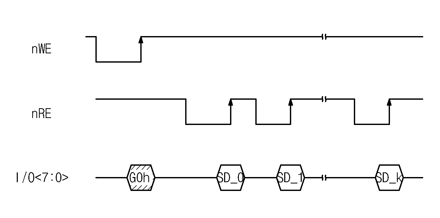
도 4는 상술한 멀티 칩 플래시 메모리 장치의 레디/비지 신호(RnB)의 출력 데이터를 간략히 보여주는 타이밍도이다. 도 4를 참조하면, 본 발명에 따른 멀티 칩 플래시 메모리 장치는 1회의 명령어(G0h)에 응답하여 모든 메모리 칩들의 레디/비지 신호(RnB)들을 할당된 입출력 핀들 각각으로 동시에 출력할 수 있다. FIG. 4 is a timing diagram briefly illustrating output data of the ready / busy signal RnB of the above-described multi-chip flash memory device. Referring to FIG. 4, the multi-chip flash memory device may simultaneously output ready / busy signals RnB of all memory chips to each of the assigned input / output pins in response to one command G0h.
메모리 칩들 각각의 프로그램 동작이나 소거 동작의 진행 여부를 확인하기 위해, 호스트나 메모리 제어기(60)는 레디/비지 신호(RnB)의 요청 명령어(G0h)를 쓰기 인에이블 신호(nWE)에 동기시켜 멀티 칩 플래시 메모리 장치로 입력한다. 레디/비지 신호(RnB)의 요청 명령어(G0h)는 입출력 라인(50)를 경유하여 각각의 메모리 칩들로 동시에 입력된다. 각각의 메모리 칩들에 포함되는 제어부(150)들은 상술한 레디/비지 신호(RnB)의 요청 명령어(G0h)를 인식한다. 각각의 메모리 칩들에 포함되는 제어부(150)들은 현재의 진행 중인 동작을 참조하여 동시에 내부 레디/비지 신호(Internal RnB)를 출력 버퍼(110)로 제공한다. 출력 버퍼(110)에 제공된 내부 레디/비지 신호(Internal RnB)는 복수의 입출력 핀(I/O Pin)들 중에 RnB 핀 지정 블록(160)에 의해서 할당된 입출력 핀(I/O<x>)으로 전달된다. In order to confirm whether a program operation or an erase operation of each of the memory chips is in progress, the host or the
다시 도면을 참조하면, 출력 버퍼(110)에 저장된 메모리 칩들의 레디/비지 신호(RnB)는 출력 인에이블 신호(nRE)의 토글링(Toggling)에 응답하여 출력된다. 즉, 각 메모리 칩들의 레디/비지 신호(RnB)에 대응하는 상태 데이터(SD_0, SD_1,…, SD_k)가 출력 인에이블 신호(nRE)의 상승 에지(Rising Edge)에 응답하여 할당된 각각의 입출력 핀(I/O<x>)으로 출력된다 여기서, 출력 인에이블 신호(nRE)의 토글링 회수는 메모리 칩들의 제어 정책에 의존함은 이 분야에서 통상의 지식을 습득한 자들에게는 자명하다. 입출력 핀으로 최초 출력되는 8비트의 레디/비지 신호(RnB)는 멀티 칩에 포함되는 메모리 칩이 8개이며, 데이터 입출력 핀(I/O<7:0>)도 8개인 경우를 예로 들어 설명하였다. 이 경우, 출력 인에이블 신호(nRE)의 1회 토글링에 의하여 입출력 핀으로 출력되는 데이터 8비트 각각은 하나의 메모리 칩의 레디/비지 신호(RnB)에 대응한다. 그리고 이러한 레디/비지 신호(RnB)들은 출력 인에이블 신호(nRE)의 토글링에 의해서 소정의 횟수 지속적으로 출력되어 호스트나 메모리 제어기(60)로 제공된다. Referring back to the drawing, the ready / busy signal RnB of the memory chips stored in the
이상의 도 4에 도시된 본 발명의 레디/비지 신호(RnB)의 출력 방법에 따르 면, 1회의 요청 명령어(G0h)의 입력으로 동시에 모든 메모리 칩들의 내부 동작 상태를 확인할 수 있는 멀티 칩 플래시 메모리 장치가 제공된다. 또한, 한 번의 명령어 제공 이후, 서로 다른 입출력 핀으로 동시에 출력되는 레디/비지 신호(RnB)들을 참조하여 메모리 제어기(60)나 호스트는 신속한 대응이 가능하다. 메모리 제어기(60)나 호스트는 각각의 메모리 칩들의 내부 동작 상태를 동시에 판단하여 대용량 데이터의 프로그램 동작과 같은 상황에서 프로그램할 칩(또는 Ready chip)을 신속하게 선택한다. 그리고 선택된 메모리 칩으로는 프로그램 데이터가 입력될 것이다. 즉, 메모리 제어기(60)나 호스트는 지속적으로 공급되는 프로그램 데이터를 기입할 메모리 칩을 신속히 파악 및 선택하여 프로그램 동작을 수행함으로써, 레디/비지 신호(RnB)를 제공받기 위한 대기 시간이 최소화될 수 있다.According to the method of outputting the ready / busy signal RnB of the present invention illustrated in FIG. 4, the multi-chip flash memory device capable of simultaneously checking the internal operating states of all the memory chips by inputting one request command G0h. Is provided. In addition, after providing a single command, the
도 5는 상술한 도 4에서 도시된 멀티 칩 플래시 메모리 장치의 레디/비지 신호들(SD_0, SD_1, SD_2,…SD_k) 각각을 구성하는 입출력 핀의 할당 정보를 예시적으로 보여주는 표이다. 도 5를 참조하면, 멀티 칩 플래시 메모리 장치에 포함되는 메모리 칩들의 입출력 핀들 각각의 레디/비지 신호(RnB)에 대한 입출력 핀(I/O<x>) 할당 정보가 예시적으로 도시되어 있다. FIG. 5 is a table illustrating allocation information of input / output pins constituting each of ready / busy signals SD_0, SD_1, SD_2,... SD_k of the multi-chip flash memory device illustrated in FIG. 4. Referring to FIG. 5, input / output pins I / O <x> allocation information of ready / busy signals RnB of respective input / output pins of memory chips included in a multi-chip flash memory device are illustrated.
칩1(Chip1)은 앞서 도시된 RnB 핀 지정 블록(160)에 의해서 할당된 입출력 핀(I/O<0>)으로 레디/비지 신호(RnB)를 출력한다. 칩1(Chip1)은 출력 인에이블 신호(nRE)에 응답하여 레디/비지 신호(RnB)를 입출력 핀(I/O<0>)으로 출력한다. 이때, 나머지 입출력 핀들(I/O<1>~I/O<7>)은 고임피던스(High-Z) 상태를 유지한다. 각각의 메모리 칩에 있어서, 레디/비지 신호(RnB)를 출력하는 핀을 제외한 나머지 입출력 핀들이 모두 고임피던스(High-Z)를 유지하는 이유는, 고임피던스(High-Z)로 설정되는 입출력 핀으로 메모리 칩들 중 어느 하나의 레디/비지 신호(RnB)가 출력되기 때문이다. 즉, 입출력 핀 I/O<4>는 칩5(Chip5)의 레디/비지 신호(RnB) 출력단으로 사용된다. 따라서, 칩5(Chip5)를 제외한 나머지 칩들은 입출력 핀 I/O<4>를 고임피던스 상태로 유지하여 칩5(Chip5)의 레디/비지 신호(RnB)가 정상적인 레벨로 출력될 수 있도록 한다. 칩2(Chip2) 내지 칩7(Chip)의 레디/비지 신호(RnB)가 출력되는 각각의 입출력 핀 할당은 상술한 도 5와 같이 순차적으로 배열될 수 있다. 그러나, 이는 예시적인 배열방법일 뿐 본 발명은 이에 국한되지 않는다. 각각의 메모리 칩들이 동일한 입출력 핀으로 레디/비지 신호(RnB)가 출력되지 않도록 입출력 핀(I/O<x>)이 할당되고 외부에서 인식할 수만 있으면 무관하다.Chip1 outputs a ready / busy signal RnB to an input / output pin I / O <0> assigned by the RnB
상술한 표와 같은 메모리 칩들의 레디/비지 신호(RnB)의 입출력 핀(I/O<x>)의 할당을 통해서, 본 발명의 멀티 칩 플래시 메모리 장치는 모든 메모리 칩들의 내부 동작의 상태를 동시에 출력할 수 있다. Through the assignment of the input / output pins I / O <x> of the ready / busy signals RnB of the memory chips as shown in the above table, the multi-chip flash memory device of the present invention simultaneously controls the state of the internal operation of all the memory chips. You can print
도 6은 본 발명의 레디/비지 신호(RnB)의 출력 방법에 따른 효과를 간략히 표현하는 타이밍도이다. 도 6을 참조하면, 호스트나 메모리 제어기(60)는 본 발명에 따른 레디/비지 신호(RnB)의 출력 방법에 따라 각각의 메모리 칩들의 내부 동작을 신속히 확인할 수 있다. 그리고 호스트나 메모리 제어기(60)는 프로그램이 종료된 메모리 칩을 신속히 감지하여 프로그램 데이터를 기입 가능한 메모리 칩으로 신속히 제공할 수 있다. 이러한 동작에 따라서, 내부의 메모리 칩들이 연속적으로 프로그램되는 인터리브 프로그램 동작시에도 프로그램 가능한 메모리 칩을 신속히 감 지할 수 있다. 프로그램 동작이 종료된 메모리 칩으로는 입력되는 프로그램 데이터가 즉시 제공됨으로써, 프로그램 동작과 프로그램 동작 사이의 시간 간격을 최소화할 수 있다. 따라서, 본 발명의 레디/비지 신호(RnB)의 출력 방법은 지속적으로 제공되는 대용량 데이터의 프로그램과 같은 인터리브 동작의 속도를 향상시킬 수 있다.6 is a timing diagram briefly expressing an effect according to an output method of the ready / busy signal RnB of the present invention. Referring to FIG. 6, the host or the
도 7은 본 발명의 멀티 칩 플래시 메모리 장치를 구비하는 시스템의 일예를 간략히 도시한 블록도이다. 도 7을 참조하면, 모바일 기기나 데스크 톱 컴퓨터와 같은 시스템에서 본 발명의 멀티 칩 플래시 메모리 장치(210)가 장착된다. 본 발명에 따른 시스템은 버스(270)에 전기적으로 연결된 중앙처리장치(230), 램(240), 입력 키보드(250), 메모리 컨트롤러(220), 그리고 플래시 메모리 장치(210)를 포함한다. 플래시 메모리 장치(210)는 앞서 언급된 멀티 칩 플래시 메모리 장치와 실질적으로 동일하게 구성될 것이다. 멀티 칩 플래시 메모리 장치(210)에는 입력 키보드(250)에 의해서 입력되거나 또는, 중앙처리장치(230)에 의해서 처리된 데이터가 메모리 제어기(220)를 통해 저장된다. 여기서, 멀티 칩 플래시 메모리 장치(210)와 메모리 제어기(220)가 별도의 구성으로 도시되었으나, 메모리 제어기(220)는 멀티 칩 플래시 메모리 장치(210)의 내부에 포함될 수 있다. 만일 본 발명의 시스템의 적용 분야가 모바일 시스템인 경우, 시스템의 구동 전압을 공급하기 위한 배터리(미도시됨)가 추가적으로 제공될 것이다. 비록 도면에는 도시되지 않았지만, 본 발명에 따른 컴퓨팅 시스템에는 응용 칩셋(Application Chipset), 카메라 이미지 프로세서(Camera Image Processor) 등이 더 제공될 수 있음은 이 분야의 통상적인 지 식을 습득한 자들에게 자명하다.7 is a block diagram schematically illustrating an example of a system having a multi-chip flash memory device of the present invention. Referring to FIG. 7, the multi-chip
본 발명의 범위 또는 기술적 사상을 벗어나지 않고 본 발명의 구조가 다양하게 수정되거나 변경될 수 있음은 이 분야에 숙련된 자들에게 자명하다. 상술한 내용을 고려하여 볼 때, 만약 본 발명의 수정 및 변경이 아래의 청구항들 및 동등 물의 범주 내에 속한다면, 본 발명이 이 발명의 변경 및 수정을 포함하는 것으로 여겨진다.It will be apparent to those skilled in the art that the structure of the present invention may be variously modified or changed without departing from the scope or spirit of the present invention. In view of the foregoing, it is believed that the present invention includes modifications and variations of this invention provided they come within the scope of the following claims and their equivalents.
상술한 본 발명의 멀티 칩 플래시 메모리 장치의 동작 방법에 따르면, 1회의 명령어 입력으로 동시에 모든 메모리 칩들의 상태 신호를 신속히 제공받을 수 있어 고속 동작이 가능한 멀티 칩 플래시 메모리 장치를 구현할 수 있다.According to the operating method of the multi-chip flash memory device of the present invention, it is possible to implement a multi-chip flash memory device capable of high-speed operation by being able to quickly receive the status signals of all the memory chips at the same time with one command input.
Claims (21)
Priority Applications (3)
| Application Number | Priority Date | Filing Date | Title |
|---|---|---|---|
| KR1020060115387A KR100843546B1 (en) | 2006-11-21 | 2006-11-21 | Multi-chip Package Flash Memory Device and Its Status Signal Reading Method |
| US11/984,595 US7843758B2 (en) | 2006-11-21 | 2007-11-20 | Multi-chip package flash memory device and method for reading status data therefrom |
| CN2007103003904A CN101226765B (en) | 2006-11-21 | 2007-11-21 | Multi-chip packaged flash memory device and reading method of status data thereof |
Applications Claiming Priority (1)
| Application Number | Priority Date | Filing Date | Title |
|---|---|---|---|
| KR1020060115387A KR100843546B1 (en) | 2006-11-21 | 2006-11-21 | Multi-chip Package Flash Memory Device and Its Status Signal Reading Method |
Publications (2)
| Publication Number | Publication Date |
|---|---|
| KR20080046003A KR20080046003A (en) | 2008-05-26 |
| KR100843546B1 true KR100843546B1 (en) | 2008-07-04 |
Family
ID=39416766
Family Applications (1)
| Application Number | Title | Priority Date | Filing Date |
|---|---|---|---|
| KR1020060115387A Active KR100843546B1 (en) | 2006-11-21 | 2006-11-21 | Multi-chip Package Flash Memory Device and Its Status Signal Reading Method |
Country Status (3)
| Country | Link |
|---|---|
| US (1) | US7843758B2 (en) |
| KR (1) | KR100843546B1 (en) |
| CN (1) | CN101226765B (en) |
Cited By (5)
| Publication number | Priority date | Publication date | Assignee | Title |
|---|---|---|---|---|
| WO2013094913A1 (en) * | 2011-12-23 | 2013-06-27 | 한양대학교 산학협력단 | Apparatus and method for controlling multi-way nand flashes by using input-output pins |
| US9147475B2 (en) | 2012-07-18 | 2015-09-29 | Samsung Electronics Co., Ltd. | Data storage device comprising nonvolatile memory chips and control method thereof |
| KR20180029432A (en) * | 2016-09-12 | 2018-03-21 | 에스케이하이닉스 주식회사 | Semiconductor memory device and operating method thereof |
| US10515704B2 (en) | 2017-10-20 | 2019-12-24 | SK Hynix Inc. | Semiconductor memory device and operating method thereof |
| US11531494B2 (en) | 2019-12-17 | 2022-12-20 | SK Hynix Inc. | Storage device and method of operating the same |
Families Citing this family (37)
| Publication number | Priority date | Publication date | Assignee | Title |
|---|---|---|---|---|
| JP4692231B2 (en) * | 2005-11-04 | 2011-06-01 | 株式会社デンソー | Electronic control device for vehicle |
| JP5253901B2 (en) | 2008-06-20 | 2013-07-31 | 株式会社東芝 | Memory system |
| US8074040B2 (en) * | 2008-09-23 | 2011-12-06 | Mediatek Inc. | Flash device and method for improving performance of flash device |
| US8266361B1 (en) * | 2009-01-28 | 2012-09-11 | Cypress Semiconductor Corporation | Access methods and circuits for devices having multiple buffers |
| KR101626084B1 (en) * | 2009-11-25 | 2016-06-01 | 삼성전자주식회사 | Multi-chip memory system and data transfer method thereof |
| US20120008445A1 (en) * | 2010-07-12 | 2012-01-12 | Promos Technologies Pte.Ltd. | Dual bit line precharge architecture and method for low power dynamic random access memory (dram) integrated circuit devices and devices incorporating embedded dram |
| KR101780422B1 (en) | 2010-11-15 | 2017-09-22 | 삼성전자주식회사 | Nonvolatile memory device, reading method thereof and memory system including the same |
| KR101893176B1 (en) * | 2010-12-03 | 2018-08-29 | 삼성전자주식회사 | Multi- chip memory device and control method thereof |
| KR101212854B1 (en) * | 2010-12-03 | 2012-12-14 | 에스케이하이닉스 주식회사 | Multi-chip package device and method for operating thereof |
| CN102543189A (en) * | 2012-02-28 | 2012-07-04 | 北京忆恒创源科技有限公司 | Semiconductor memory, interface circuit and access method thereof |
| US9336112B2 (en) * | 2012-06-19 | 2016-05-10 | Apple Inc. | Parallel status polling of multiple memory devices |
| US9740485B2 (en) | 2012-10-26 | 2017-08-22 | Micron Technology, Inc. | Apparatuses and methods for memory operations having variable latencies |
| US9754648B2 (en) | 2012-10-26 | 2017-09-05 | Micron Technology, Inc. | Apparatuses and methods for memory operations having variable latencies |
| JP2014149669A (en) * | 2013-01-31 | 2014-08-21 | Toshiba Corp | Semiconductor memory device |
| US9734097B2 (en) | 2013-03-15 | 2017-08-15 | Micron Technology, Inc. | Apparatuses and methods for variable latency memory operations |
| US9727493B2 (en) | 2013-08-14 | 2017-08-08 | Micron Technology, Inc. | Apparatuses and methods for providing data to a configurable storage area |
| JP2015069602A (en) * | 2013-09-30 | 2015-04-13 | 株式会社東芝 | Memory system |
| US9245633B2 (en) * | 2014-01-22 | 2016-01-26 | Htc Corporation | Storage device, electronic device, and method for programming memory |
| JP2015197859A (en) * | 2014-04-02 | 2015-11-09 | 株式会社東芝 | Memory controller, semiconductor memory device, and memory controller control method |
| US10365835B2 (en) | 2014-05-28 | 2019-07-30 | Micron Technology, Inc. | Apparatuses and methods for performing write count threshold wear leveling operations |
| KR102229970B1 (en) * | 2014-06-27 | 2021-03-22 | 삼성전자주식회사 | Solid state drive including nonvolatile memory, random access memory and memory controller |
| US9959078B2 (en) | 2015-01-30 | 2018-05-01 | Sandisk Technologies Llc | Multi-die rolling status mode for non-volatile storage |
| US10114690B2 (en) * | 2015-02-13 | 2018-10-30 | Sandisk Technologies Llc | Multi-die status mode for non-volatile storage |
| US10552047B2 (en) * | 2015-02-23 | 2020-02-04 | Toshiba Memory Corporation | Memory system |
| US10095412B2 (en) * | 2015-11-12 | 2018-10-09 | Sandisk Technologies Llc | Memory system and method for improving write performance in a multi-die environment |
| KR20170086345A (en) * | 2016-01-18 | 2017-07-26 | 에스케이하이닉스 주식회사 | Memory system having memory chip and memory controller |
| US10467148B2 (en) * | 2016-06-16 | 2019-11-05 | SK Hynix Inc. | System of multiple configurations and operating method thereof |
| KR20190018326A (en) * | 2017-08-14 | 2019-02-22 | 에스케이하이닉스 주식회사 | Memory system and operation method for the same |
| JP2019040470A (en) * | 2017-08-25 | 2019-03-14 | 東芝メモリ株式会社 | Memory system |
| KR102182718B1 (en) * | 2018-05-24 | 2020-11-25 | 에센코어 리미티드 | Memory device, the control method of the memory device and the method for controlling the memory device |
| CN109461468B (en) * | 2018-11-14 | 2021-05-11 | 深圳芯邦科技股份有限公司 | Data stability detection method |
| KR102812909B1 (en) * | 2019-08-16 | 2025-05-26 | 구글 엘엘씨 | Synchronization of multi-chip systems |
| KR102822665B1 (en) * | 2020-06-15 | 2025-06-20 | 에스케이하이닉스 주식회사 | Memory device and method for operating the same |
| US11586393B2 (en) * | 2020-12-30 | 2023-02-21 | Macronix International Co., Ltd. | Control method for requesting status of flash memory, flash memory die and flash memory with the same |
| KR102481649B1 (en) | 2021-12-01 | 2022-12-28 | 삼성전자주식회사 | Nonvolatile memory device, controller for controlling the same, storage device having the same, and operating method thereof |
| CN115469933A (en) * | 2022-08-10 | 2022-12-13 | 厦门市美亚柏科信息股份有限公司 | Automatic data extraction system for memory chip |
| TWI824843B (en) * | 2022-11-24 | 2023-12-01 | 慧榮科技股份有限公司 | Control method of memory device and associated flash memory controller and memory device |
Citations (1)
| Publication number | Priority date | Publication date | Assignee | Title |
|---|---|---|---|---|
| US20040057297A1 (en) * | 2002-07-09 | 2004-03-25 | Cheol-Ung Jang | Multiple chip system including a plurality of non-volatile semiconductor memory devices |
Family Cites Families (11)
| Publication number | Priority date | Publication date | Assignee | Title |
|---|---|---|---|---|
| JP3310011B2 (en) * | 1992-03-30 | 2002-07-29 | 株式会社東芝 | Semiconductor memory and semiconductor memory board using the same |
| JPH11126497A (en) * | 1997-10-22 | 1999-05-11 | Oki Electric Ind Co Ltd | Non-volatile semiconductor memory |
| JP2001167586A (en) | 1999-12-08 | 2001-06-22 | Toshiba Corp | Nonvolatile semiconductor memory device |
| KR20020044907A (en) * | 2000-12-07 | 2002-06-19 | 윤종용 | Method for programming in multi-flash memory system |
| TW561491B (en) * | 2001-06-29 | 2003-11-11 | Toshiba Corp | Semiconductor memory device |
| JP4157559B2 (en) | 2001-06-29 | 2008-10-01 | 株式会社東芝 | Semiconductor memory device |
| US6798696B2 (en) * | 2001-12-04 | 2004-09-28 | Renesas Technology Corp. | Method of controlling the operation of non-volatile semiconductor memory chips |
| US7287115B2 (en) * | 2003-10-30 | 2007-10-23 | Kabushiki Kaisha Toshiba | Multi-chip package type memory system |
| US7701764B2 (en) * | 2006-05-17 | 2010-04-20 | Micron Technology, Inc. | Apparatus and method for reduced peak power consumption during common operation of multi-NAND flash memory devices |
| KR100764749B1 (en) * | 2006-10-03 | 2007-10-08 | 삼성전자주식회사 | Multi-chip Package Flash Memory Device and Its Copyback Method |
| KR100816119B1 (en) * | 2006-12-28 | 2008-03-21 | 주식회사 하이닉스반도체 | Multi die package device |
-
2006
- 2006-11-21 KR KR1020060115387A patent/KR100843546B1/en active Active
-
2007
- 2007-11-20 US US11/984,595 patent/US7843758B2/en active Active
- 2007-11-21 CN CN2007103003904A patent/CN101226765B/en active Active
Patent Citations (2)
| Publication number | Priority date | Publication date | Assignee | Title |
|---|---|---|---|---|
| US20040057297A1 (en) * | 2002-07-09 | 2004-03-25 | Cheol-Ung Jang | Multiple chip system including a plurality of non-volatile semiconductor memory devices |
| US6888733B2 (en) * | 2002-07-09 | 2005-05-03 | Samsung Electronics Co., Ltd. | Multiple chip system including a plurality of non-volatile semiconductor memory devices |
Non-Patent Citations (2)
| Title |
|---|
| ''Surendra Burman et al., Programmable Multichip Modules, IEEE Micro, pp. 28-35, April 1993'' * |
| Surendra Burman et al., Programmable Multichip Modules, IEEE Micro, pp. 28-35, April 1993 * |
Cited By (6)
| Publication number | Priority date | Publication date | Assignee | Title |
|---|---|---|---|---|
| WO2013094913A1 (en) * | 2011-12-23 | 2013-06-27 | 한양대학교 산학협력단 | Apparatus and method for controlling multi-way nand flashes by using input-output pins |
| US9147475B2 (en) | 2012-07-18 | 2015-09-29 | Samsung Electronics Co., Ltd. | Data storage device comprising nonvolatile memory chips and control method thereof |
| KR20180029432A (en) * | 2016-09-12 | 2018-03-21 | 에스케이하이닉스 주식회사 | Semiconductor memory device and operating method thereof |
| KR102603243B1 (en) * | 2016-09-12 | 2023-11-16 | 에스케이하이닉스 주식회사 | Semiconductor memory device and operating method thereof |
| US10515704B2 (en) | 2017-10-20 | 2019-12-24 | SK Hynix Inc. | Semiconductor memory device and operating method thereof |
| US11531494B2 (en) | 2019-12-17 | 2022-12-20 | SK Hynix Inc. | Storage device and method of operating the same |
Also Published As
| Publication number | Publication date |
|---|---|
| CN101226765B (en) | 2013-01-30 |
| KR20080046003A (en) | 2008-05-26 |
| US7843758B2 (en) | 2010-11-30 |
| US20080117682A1 (en) | 2008-05-22 |
| CN101226765A (en) | 2008-07-23 |
Similar Documents
| Publication | Publication Date | Title |
|---|---|---|
| KR100843546B1 (en) | Multi-chip Package Flash Memory Device and Its Status Signal Reading Method | |
| US10379903B2 (en) | Task queues | |
| TWI641952B (en) | Memory device, method, and computer program product | |
| CN102723099B (en) | Including for processing many command descriptor blocks so that the flash memory device of the HPI using concurrency | |
| US6445615B2 (en) | Non-volatile semiconductor memory device and semiconductor disk device | |
| US8429374B2 (en) | System and method for read-while-write with NAND memory device | |
| CN1322441C (en) | Multi-chip package type memory system | |
| JP2015164090A (en) | multiple independent serial link memory | |
| KR100442091B1 (en) | Multi-chip capable of ensuring each operation of embedded chips | |
| JP2001167586A (en) | Nonvolatile semiconductor memory device | |
| US20220350655A1 (en) | Controller and memory system having the same | |
| US11742004B2 (en) | Memory supporting multiple types of operations | |
| US12591380B2 (en) | Storage device and operating method thereof | |
| US20070028037A1 (en) | Memory system with automatic dual-buffering | |
| JP4230886B2 (en) | Multi-chip packaged memory system | |
| US12411636B2 (en) | Storage device and method to check statuses of memory devices | |
| EP4650974A1 (en) | A storage system and operating method of the same | |
| KR100910944B1 (en) | Flash memory control device and method for sharing control signals | |
| KR102242957B1 (en) | High speed NAND memory system and high speed NAND memory package device | |
| CN117762346A (en) | Memory reading method, memory storage device and memory controller | |
| KR20220048303A (en) | An operating method of host device and storage device using a credit | |
| HK1172443A (en) | Flash memory device comprising host interface for processing a multi-command descriptor block in order to exploit concurrency |
Legal Events
| Date | Code | Title | Description |
|---|---|---|---|
| A201 | Request for examination | ||
| PA0109 | Patent application |
Patent event code: PA01091R01D Comment text: Patent Application Patent event date: 20061121 |
|
| PA0201 | Request for examination | ||
| E902 | Notification of reason for refusal | ||
| PE0902 | Notice of grounds for rejection |
Comment text: Notification of reason for refusal Patent event date: 20071214 Patent event code: PE09021S01D |
|
| PG1501 | Laying open of application | ||
| E701 | Decision to grant or registration of patent right | ||
| PE0701 | Decision of registration |
Patent event code: PE07011S01D Comment text: Decision to Grant Registration Patent event date: 20080624 |
|
| GRNT | Written decision to grant | ||
| PR0701 | Registration of establishment |
Comment text: Registration of Establishment Patent event date: 20080627 Patent event code: PR07011E01D |
|
| PR1002 | Payment of registration fee |
Payment date: 20080630 End annual number: 3 Start annual number: 1 |
|
| PG1601 | Publication of registration | ||
| PR1001 | Payment of annual fee |
Payment date: 20110531 Start annual number: 4 End annual number: 4 |
|
| PR1001 | Payment of annual fee |
Payment date: 20120531 Start annual number: 5 End annual number: 5 |
|
| FPAY | Annual fee payment |
Payment date: 20130531 Year of fee payment: 6 |
|
| PR1001 | Payment of annual fee |
Payment date: 20130531 Start annual number: 6 End annual number: 6 |
|
| FPAY | Annual fee payment |
Payment date: 20140530 Year of fee payment: 7 |
|
| PR1001 | Payment of annual fee |
Payment date: 20140530 Start annual number: 7 End annual number: 7 |
|
| FPAY | Annual fee payment |
Payment date: 20150601 Year of fee payment: 8 |
|
| PR1001 | Payment of annual fee |
Payment date: 20150601 Start annual number: 8 End annual number: 8 |
|
| FPAY | Annual fee payment |
Payment date: 20160531 Year of fee payment: 9 |
|
| PR1001 | Payment of annual fee |
Payment date: 20160531 Start annual number: 9 End annual number: 9 |
|
| FPAY | Annual fee payment |
Payment date: 20190530 Year of fee payment: 12 |
|
| PR1001 | Payment of annual fee |
Payment date: 20190530 Start annual number: 12 End annual number: 12 |
|
| PR1001 | Payment of annual fee |
Payment date: 20230524 Start annual number: 16 End annual number: 16 |
|
| PR1001 | Payment of annual fee |
Payment date: 20240527 Start annual number: 17 End annual number: 17 |