KR100774840B1 - Semiconductor package and manufacturing method thereof - Google Patents
Semiconductor package and manufacturing method thereof Download PDFInfo
- Publication number
- KR100774840B1 KR100774840B1 KR1020010005173A KR20010005173A KR100774840B1 KR 100774840 B1 KR100774840 B1 KR 100774840B1 KR 1020010005173 A KR1020010005173 A KR 1020010005173A KR 20010005173 A KR20010005173 A KR 20010005173A KR 100774840 B1 KR100774840 B1 KR 100774840B1
- Authority
- KR
- South Korea
- Prior art keywords
- semiconductor package
- bonding
- vent
- vent path
- vent hole
- Prior art date
- Legal status (The legal status is an assumption and is not a legal conclusion. Google has not performed a legal analysis and makes no representation as to the accuracy of the status listed.)
- Expired - Fee Related
Links
Images


Classifications
-
- H—ELECTRICITY
- H10—SEMICONDUCTOR DEVICES; ELECTRIC SOLID-STATE DEVICES NOT OTHERWISE PROVIDED FOR
- H10W—GENERIC PACKAGES, INTERCONNECTIONS, CONNECTORS OR OTHER CONSTRUCTIONAL DETAILS OF DEVICES COVERED BY CLASS H10
- H10W70/00—Package substrates; Interposers; Redistribution layers [RDL]
- H10W70/60—Insulating or insulated package substrates; Interposers; Redistribution layers
-
- H—ELECTRICITY
- H10—SEMICONDUCTOR DEVICES; ELECTRIC SOLID-STATE DEVICES NOT OTHERWISE PROVIDED FOR
- H10W—GENERIC PACKAGES, INTERCONNECTIONS, CONNECTORS OR OTHER CONSTRUCTIONAL DETAILS OF DEVICES COVERED BY CLASS H10
- H10W72/00—Interconnections or connectors in packages
- H10W72/851—Dispositions of multiple connectors or interconnections
- H10W72/874—On different surfaces
- H10W72/884—Die-attach connectors and bond wires
-
- H—ELECTRICITY
- H10—SEMICONDUCTOR DEVICES; ELECTRIC SOLID-STATE DEVICES NOT OTHERWISE PROVIDED FOR
- H10W—GENERIC PACKAGES, INTERCONNECTIONS, CONNECTORS OR OTHER CONSTRUCTIONAL DETAILS OF DEVICES COVERED BY CLASS H10
- H10W90/00—Package configurations
- H10W90/701—Package configurations characterised by the relative positions of pads or connectors relative to package parts
- H10W90/731—Package configurations characterised by the relative positions of pads or connectors relative to package parts of die-attach connectors
- H10W90/734—Package configurations characterised by the relative positions of pads or connectors relative to package parts of die-attach connectors between a chip and a stacked insulating package substrate, interposer or RDL
-
- H—ELECTRICITY
- H10—SEMICONDUCTOR DEVICES; ELECTRIC SOLID-STATE DEVICES NOT OTHERWISE PROVIDED FOR
- H10W—GENERIC PACKAGES, INTERCONNECTIONS, CONNECTORS OR OTHER CONSTRUCTIONAL DETAILS OF DEVICES COVERED BY CLASS H10
- H10W90/00—Package configurations
- H10W90/701—Package configurations characterised by the relative positions of pads or connectors relative to package parts
- H10W90/751—Package configurations characterised by the relative positions of pads or connectors relative to package parts of bond wires
- H10W90/754—Package configurations characterised by the relative positions of pads or connectors relative to package parts of bond wires between a chip and a stacked insulating package substrate, interposer or RDL
Landscapes
- Structures Or Materials For Encapsulating Or Coating Semiconductor Devices Or Solid State Devices (AREA)
- Encapsulation Of And Coatings For Semiconductor Or Solid State Devices (AREA)
Abstract
본 발명은 반도체 패키지 내부의 습기를 방출시키기 위하여 부재에 벤트홀이 형성된 반도체 패키지에 있어서, 내부의 습기를 보다 효율적으로 방출시키기 위하여 접착수단에 벤트경로가 형성된 구조의 반도체 패키지 및 그 제조 방법에 관한 것이다.The present invention relates to a semiconductor package having a vent hole formed in a member for releasing moisture in a semiconductor package, and to a semiconductor package having a structure in which a vent path is formed in an adhesive means for releasing moisture therein more efficiently. will be.
이에, 벤트홀이 형성된 부재의 칩탑재영역에 격자형 벤트경로를 갖는 접착수단을 부착하여, 접착수단의 벤트경로와 부재의 벤트홀이 서로 연통되도록 함으로써, 패키지 내부에 깊숙히 잔존하는 습기까지 보다 효율적으로 방출시킬 수 있는 장점을 제공하고자 한 것이다.
Therefore, by attaching a bonding means having a lattice-like vent path in the chip mounting region of the member where the vent hole is formed, the vent path of the bonding means and the vent hole of the member communicate with each other, thereby more efficiently even the moisture remaining deep inside the package. It is intended to provide an advantage that can be released.
반도체 패키지, 벤트홀, 벤트경로, 접착수단, 인쇄회로기판, 습기, 방출Semiconductor package, vent hole, vent path, adhesive means, printed circuit board, moisture, discharge
Description
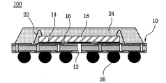
도 1은 본 발명에 따른 반도체 패키지를 나타내는 단면도,1 is a cross-sectional view showing a semiconductor package according to the present invention;
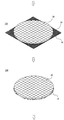
도 2는 본 발명에 따른 반도체 패키지에 있어서, 부재와 접착수단과 반도체 칩간의 접착상태를 보여주는 분리 사시도,2 is an exploded perspective view showing an adhesive state between a member, an adhesive means, and a semiconductor chip in the semiconductor package according to the present invention;
도 3a,3b,3c,3d는 본 발명에 따른 반도체 패키지의 제조방법을 순서대로 나타내는 도면,3A, 3B, 3C, and 3D are diagrams sequentially illustrating a method of manufacturing a semiconductor package according to the present invention;
도 4는 종래의 반도체 패키지 구조를 나타내는 단면도.4 is a cross-sectional view showing a conventional semiconductor package structure.
<도면의 주요 부분에 대한 부호의 설명><Explanation of symbols for main parts of the drawings>
10 : 인쇄회로기판 12 : 벤트홀10: printed circuit board 12: vent hole
14 : 접착수단 16 : 벤트경로14: bonding means 16: vent path
18 : 반도체 칩 20 : 웨이퍼18: semiconductor chip 20: wafer
22 : 와이어 24 : 수지22: wire 24: resin
26 : 인출단자 28 : 지지용 필름26: withdrawal terminal 28: support film
100,200 : 반도체 패키지
100,200: Semiconductor Package
본 발명은 반도체 패키지 및 그 제조 방법에 관한 것으로, 더욱 상세하게는 반도체 패키지 내부의 습기를 방출시키기 위하여 부재에 벤트홀이 형성된 반도체 패키지에 있어서, 내부의 습기를 보다 효율적으로 방출시키기 위하여 접착수단에 벤트경로가 형성된 구조의 반도체 패키지 및 그 제조 방법에 관한 것이다.BACKGROUND OF THE INVENTION 1. Field of the Invention The present invention relates to a semiconductor package and a method of manufacturing the same. More particularly, in a semiconductor package in which a vent hole is formed in a member for releasing moisture inside the semiconductor package, A semiconductor package having a structure in which a vent path is formed and a method of manufacturing the same.
일반적으로 반도체 패키지는 리드프레임, 인쇄회로기판, 회로필름등의 부재를 사용하여, 열방출 성능을 향상시킬 수 있고, 칩의 크기에 가깝게 경박단소화를 실현할 수 있으며, 입출력 단자수를 증가시킬 수 있는 등 그 밖에 여러가지 형태로 성능 향상에 기여할 수 있는 구조로 제조되고 있다.In general, a semiconductor package uses members such as a lead frame, a printed circuit board, and a circuit film to improve heat dissipation performance, to realize light and thin shortening close to the size of a chip, and to increase the number of input / output terminals. It is manufactured in a structure that can contribute to performance improvement in various forms.
또한, 반도체 패키지 내부에 잔존하는 습기를 배출시킬 수 있도록 인쇄회로기판의 칩탑재영역에 벤트홀이 형성된 구조의 반도체 패키지가 제조되고 있다.In addition, a semiconductor package having a structure in which a vent hole is formed in a chip mounting region of a printed circuit board to discharge moisture remaining in the semiconductor package is manufactured.
통상, 반도체 패키지의 내부에서 습기가 존재하는 이유는 반도체 패키지의 제조공정 중에 여러가지 경로로 침투하여 잔존할 수 있고, 특히 부재의 칩탑재영역에 에폭시 또는 접착테이프와 같은 접착수단으로 반도체 칩을 부착하는 공정에 있어서, 반도체 칩과 접착수단 사이가 완전하게 밀착되며 부착되지 않고, 일부분에 작은 공동(空洞)이 형성되며 부착되어, 상기 공동으로 접착수단이 보유하고 있던 습기등이 유출되어 잔존할 수 있다.In general, the reason for the presence of moisture in the semiconductor package is that it can penetrate and remain in various ways during the manufacturing process of the semiconductor package, and in particular, the semiconductor chip is attached to the chip mounting region of the member by an adhesive means such as epoxy or adhesive tape. In the process, the space between the semiconductor chip and the bonding means is completely adhered and not attached, but a small cavity is formed and attached to a portion thereof, and the moisture or the like held by the bonding means may leak out and remain in the cavity. .
특히, 반도체 패키지의 내부에 잔존하는 습기는 몰딩수지를 경화시키는 과정 에서, 즉 반도체 패키지의 몰딩공정 후, 반도체 패키지를 오븐에 넣고, 몰딩수지를 경화(Cure)시키는 과정에서 심하게 일어나는데, 상기 몰딩수지의 경화시에 오븐의 경화 온도는 180℃ 정도의 고온이기 때문에 내부에 잔존하는 습기가 기화되면서 크게 팽창(약 1000배)된다.In particular, the moisture remaining inside the semiconductor package occurs badly during curing of the molding resin, that is, after the semiconductor package molding process, the semiconductor package is placed in an oven, and the molding resin is cured. Since the curing temperature of the oven is about 180 ° C. at the time of curing, the moisture remaining inside is greatly expanded (about 1000 times) as the vaporizes.
그에따라, 상기 습기가 팽창되면서, 반도체 칩과 접착수단 또는 접착수단과 부재의 칩탑재영역간의 디라미네이션(Delamination) 현상이 일어나서, 결국 반도체 칩에 균열이 발생하는 등 반도체 패키지의 불량을 초래하는 문제점이 있었다.Accordingly, as the moisture expands, a delamination phenomenon occurs between the semiconductor chip and the adhesive means or the chip mounting region of the adhesive means, resulting in a defect of the semiconductor package such as a crack in the semiconductor chip. There was this.
따라서, 상기 습기를 외부로 방출시켜 반도체 패키지의 불량을 방지할 수 있도록 첨부한 도 4에 도시한 바와 같은 구조의 반도체 패키지가 제조되고 있는데, 그 구조를 설명하면 다음과 같다.Therefore, a semiconductor package having a structure as shown in FIG. 4 is manufactured so as to release the moisture to the outside to prevent a defect of the semiconductor package. The structure of the semiconductor package is as follows.
상기 반도체 패키지(200)는: 칩탑재영역에 벤트홀(12)이 형성된 인쇄회로기판(10)과 같은 반도체 패키지 제조용 부재와; 상기 벤트홀(12)을 제외한 부재의 칩탑재영역에 도포되는 접착수단(14)과; 상기 접착수단(14)상에 부착되는 반도체 칩(18)과; 상기 부재의 와이어 본딩영역과 상기 반도체 칩의 본딩패드간에 연결된 와이어(22)와; 상기 반도체 칩(18)과 와이어(22)을 포함하는 부재의 상면에 걸쳐 몰딩된 수지(24)와; 상기 부재의 저면으로 노출된 인출단자 부착용 전도성패턴에 융착된 인출단자(26)등으로 구성되어 있다.The
이때, 상기 벤트홀(12)과 일치되는 반도체 칩(18)의 저면 중앙부가 벤트홀을 통하여 외부로 노출된 상태가 된다.At this time, the center portion of the bottom surface of the
따라서, 상기 반도체 패키지(200)의 내부에 잔존하는 습기가 상기 인쇄회로 기판(10)의 벤트홀(12)을 통하여 외부로 방출됨으로써, 종래에 습기에 의한 디라미네이션 현상등을 방지할 수 있게 된다.Therefore, the moisture remaining in the
그러나, 상기 벤트홀과 일치되는 부분을 제외하고, 상기 접착수단과 반도체 칩 또는 접착수단과 부재의 칩탑재영역간의 접촉면적이 안쪽으로 넓게 분포된 상태이기 때문에, 상기 벤트홀을 중심으로 패키지 내부의 깊숙한 곳에 잔존하는 습기까지 보다 효율적으로 방출시킬 수 있는 반도체 패키지의 습기 방출 구조가 요구되고 있다.
However, the contact area between the bonding means and the semiconductor chip or the chip mounting region of the bonding means and the member is distributed inward, except for a portion coinciding with the vent hole. There is a need for a moisture releasing structure of a semiconductor package that can more efficiently release moisture remaining deep.
따라서, 본 발명은 상기와 같은 점을 감안하여, 반도체 패키지 내부에 잔존하는 습기를 부재의 벤트홀을 통하여 보다 효율적으로 방출시킬 수 있는 구조의 반도체 패키지 및 그 제조 방법을 제공하는데 그 목적이 있다.Accordingly, an object of the present invention is to provide a semiconductor package having a structure capable of more efficiently releasing moisture remaining in a semiconductor package through a vent hole of a member, and a method of manufacturing the same.
이에, 벤트홀이 형성된 부재의 칩탑재영역에 격자형 벤트경로를 갖는 접착수단을 부착하여, 접착수단의 벤트경로와 부재의 벤트홀이 서로 연통되도록 함으로써, 패키지 내부에 잔존하는 습기를 보다 효율적으로 방출시킬 수 있는 장점을 제공하고자 한 것이다.
Therefore, by attaching an adhesive means having a lattice-like vent path to the chip mounting region of the member where the vent hole is formed, the vent path of the adhesive means and the vent hole of the member communicate with each other, thereby efficiently absorbing moisture remaining in the package. It is to provide an advantage that can be released.
상기한 목적을 달성하기 위한 본 발명은: The present invention for achieving the above object is:
칩탑재영역에 벤트홀이 형성된 반도체 패키지 제조용 부재와; 상기 벤트홀을 제외한 부재의 칩탑재영역에 도포되는 접착수단과; 상기 접착수단상에 부착되는 반도체 칩과; 상기 부재의 와이어 본딩영역과 상기 반도체 칩의 본딩패드간에 연결된 와이어와; 상기 반도체 칩과 와이어을 포함하는 부재의 상면에 걸쳐 몰딩된 수지등으로 구성되어 있는 반도체 패키지에 있어서, A semiconductor package manufacturing member having a vent hole formed in a chip mounting region; Bonding means applied to the chip mounting area of the member except for the vent hole; A semiconductor chip attached on the bonding means; A wire connected between the wire bonding region of the member and the bonding pad of the semiconductor chip; In a semiconductor package composed of a resin and the like molded over the upper surface of the member including the semiconductor chip and the wire,
상기 접착수단에 여러갈래로 연통된 벤트경로를 형성하되, 이 벤트경로는 상기 부재의 벤트홀과 연통되게 형성시킨 것을 특징으로 하는 반도체 패키지를 제공한다.A vent path is formed to communicate with the adhesive means in several ways, and the vent path is provided to be in communication with the vent hole of the member.
삭제delete
상기한 목적을 달성하기 위한 본 발명의 반도체 패키지 제조방법은:The semiconductor package manufacturing method of the present invention for achieving the above object is:
소정의 면적을 갖는 지지용 필름상에 접착수단을 부착하는 단계와; 상기 접착수단에 벤트경로를 형성하되, 이 벤트경로가 형성될 부분에 에칭액을 분사하여 제거해주는 에칭 처리 방법 또는 절개수단으로 절개하는 방법으로 벤트경로를 형성하는 단계와; 상기 벤트경로가 형성된 접착수단상에 웨이퍼를 부착하는 단계와; 상기 지지용 필름을 떼어내는 단계와; 상기 웨이퍼를 접착수단과 함께 개개의 칩으로 소잉하는 단계와; 상기 접착수단이 저면에 부착된 상태로 소잉된 개개의 칩을 벤트홀이 형성된 부재의 칩탑재영역에 부착하는 단계와; 상기 부재의 와이어 본딩영역과 상기 반도체 칩의 본딩패드간을 와이어로 본딩하는 단계와; 상기 반도체 칩과 와이어등을 포함하는 부재의 상면에 걸쳐 수지로 몰딩하는 단계로 이루어진 것을 특징으로 한다.Attaching an adhesive means on a supporting film having a predetermined area; Forming a vent path in the bonding means, and forming the vent path by an etching treatment method or a method of cutting the etching solution to remove the etching solution in a portion where the vent path is to be formed; Attaching a wafer on an adhesive means in which the vent path is formed; Removing the supporting film; Sawing the wafer into individual chips with bonding means; Attaching each chip sawed with the adhesive means attached to a bottom surface to a chip mounting region of a member in which a vent hole is formed; Bonding between the wire bonding region of the member and the bonding pad of the semiconductor chip with a wire; And molding a resin over the upper surface of the member including the semiconductor chip and the wire.
삭제delete
삭제delete
여기서 본 발명의 실시예를 첨부한 도면에 의거하여 보다 상세하게 설명하면 다음과 같다.Hereinafter, the embodiments of the present invention will be described in detail with reference to the accompanying drawings.
첨부한 도 3a,3b,3c,3d는 본 발명에 따른 반도체 패키지의 제조 방법을 순서대로 나타내는 도면이고, 도 2는 인쇄회로기판의 칩탑재영역과 접착수단과 반도체 칩이 서로 부착되는 상태를 나타내는 분리 사시도이고, 도 1은 본 발명의 제조방법에 따라 제조된 반도체 패키지를 나타낸다.3A, 3B, 3C, and 3D are diagrams sequentially illustrating a method of manufacturing a semiconductor package according to the present invention, and FIG. 2 is a view illustrating a state in which a chip mounting region, a bonding means, and a semiconductor chip of a printed circuit board are attached to each other. 1 is an exploded perspective view, and FIG. 1 shows a semiconductor package manufactured according to the manufacturing method of the present invention.
우선, 소정의 면적을 갖는 지지용 필름(28)상에 양면 접착테이프와 같은 접착수단(14)을 부착시키는 단계(110)를 진행시키는 바, 상기 지지용 필름(28)의 면적은 웨이퍼의 크기보다 큰 것을 사용한다.First, the
다음으로, 상기 접착수단(14)에 벤트경로(16)를 형성하는 단계(120)를 진행시키게 되는데, 상기 벤트경로(16)는 사각구조의 격자형 또는 엑스(X)자형, 방사형 구조등 여러가지 형태로 형성하여도 무방하고, 서로 연통되게 형성하는 것이 바람직하다.Next, the
상기 벤트경로(16)를 형성하는 방법은 접착수단(14)상에 벤트경로(16)가 형성될 부분을 제외한 영역에 에칭되지 않는 레지스트(미도시됨)를 부착한 후, 벤트경로(16)가 형성될 영역에 에칭액을 분사하여 이루어지는 에칭(Etching) 처리 방법또는 칼, 블레이드와 같은 절개수단을 사용하여 벤트경로(16)가 형성될 영역을 절개하는 등의 방법을 사용하는 것이 바람직하다.The
다음으로, 상기 벤트경로(16)가 형성된 접착수단(14)상에 개개의 칩이 집적 되어 있는 웨이퍼(20)를 부착하는 단계(130)와, 상기 접착수단(14)으로부터 지지용 필름(28)을 떼어내는 단계(140)를 진행하게 된다.Next, attaching the
이때, 상기 웨이퍼(20)의 백면이 접착수단(14)과 부착되도록 한다.At this time, the back surface of the
다음으로, 상기 웨이퍼(20)를 접착수단(14)과 함께 개개의 칩 단위별로 소잉하는 단계(150)를 진행하는 바, 개개의 칩(18) 저면에는 벤트경로(16)를 갖는 접착수단(14)이 부착된 상태가 된다.Next, a
이어서, 상기 접착수단(14)이 저면에 부착된 상태로 소잉된 개개의 칩(18)을 벤트홀(12)이 형성된 인쇄회로기판(10)의 칩탑재영역에 부착하는 단계(160)를 진행하게 되면, 상기 접착수단(14)의 벤트경로(16)와 인쇄회로기판(10)의 벤트홀(12)은 서로 연통된 상태가 된다.Subsequently, the
계속해서, 상기 인쇄회로기판(10)의 와이어 본딩용 전도성패턴과, 상기 반도체 칩(18)의 본딩패드간을 와이어(22)로 본딩하는 단계(170)와; 상기 반도체 칩(18)과 와이어(22)등을 포함하는 인쇄회로기판(10)의 상면에 걸쳐 수지(24)로 몰딩하는 단계(180)와; 상기 인쇄회로기판(10)의 저면으로 노출된 인출단자 부착용 전도성패턴에 전도성의 솔더볼과 같은 인출단자(26)를 융착하는 단계(190)를 진행함으로써, 첨부한 도 1에 도시한 본 발명의 반도체 패키지(100)로 제조된다.Subsequently, bonding (170) between the wire bonding conductive pattern of the printed circuit board (10) and the bonding pad of the semiconductor chip (18); Molding (180) the resin (24) over the upper surface of the printed circuit board (10) including the semiconductor chip (18) and wire (22); The semiconductor of the present invention as illustrated in FIG. 1 is attached by performing a
이에따라, 상기 반도체 패키지(100)의 내부에 깊숙히 잔존하는 습기까지 서로 연통된 상태인 상기 접착수단(14)의 벤트경로(16)와 인쇄회로기판(10)의 벤트홀(12)을 경유하여 외부로 용이하게 방출되어, 종래에 습기에 의한 반도체 패키지의 불량을 방지할 수 있게 된다.Accordingly, the outside of the
이상에서 본 바와 같이, 본 발명에 따른 반도체 패키지 및 그 제조 방법에 의하면, 부재의 칩탑재영역에 반도체 칩을 부착하는 접착수단에 격자형 벤트경로를 형성하여, 부재의 칩탑재영역에 형성된 벤트홀과 서로 연통되도록 함으로써, 반도체 패키지의 내부에 잔존하는 습기를 보다 효율적으로 외부로 방출시킬 수 있는 장점을 제공한다.As described above, according to the semiconductor package according to the present invention and a method of manufacturing the same, a vent hole formed in the chip mounting region of the member is formed by forming a lattice vent path on the bonding means for attaching the semiconductor chip to the chip mounting region of the member. By communicating with each other, it provides an advantage that the moisture remaining in the inside of the semiconductor package can be more efficiently released to the outside.
그에따라, 종래에 내부에 잔존하는 습기에 의하여 반도체 칩과 접착수단, 또는 접착수단과 칩탑재영역간에 디라미네이션 형상이 발생하던 점을 방지할 수 있어, 결국 반도체 패키지의 불량을 방지할 수 있게 된다.Accordingly, it is possible to prevent the occurrence of the delamination shape between the semiconductor chip and the bonding means, or between the bonding means and the chip mounting region due to the moisture remaining in the prior art, thereby preventing the defect of the semiconductor package. .
Claims (4)
Priority Applications (1)
| Application Number | Priority Date | Filing Date | Title |
|---|---|---|---|
| KR1020010005173A KR100774840B1 (en) | 2001-02-02 | 2001-02-02 | Semiconductor package and manufacturing method thereof |
Applications Claiming Priority (1)
| Application Number | Priority Date | Filing Date | Title |
|---|---|---|---|
| KR1020010005173A KR100774840B1 (en) | 2001-02-02 | 2001-02-02 | Semiconductor package and manufacturing method thereof |
Publications (2)
| Publication Number | Publication Date |
|---|---|
| KR20020064592A KR20020064592A (en) | 2002-08-09 |
| KR100774840B1 true KR100774840B1 (en) | 2007-11-07 |
Family
ID=27693178
Family Applications (1)
| Application Number | Title | Priority Date | Filing Date |
|---|---|---|---|
| KR1020010005173A Expired - Fee Related KR100774840B1 (en) | 2001-02-02 | 2001-02-02 | Semiconductor package and manufacturing method thereof |
Country Status (1)
| Country | Link |
|---|---|
| KR (1) | KR100774840B1 (en) |
Cited By (1)
| Publication number | Priority date | Publication date | Assignee | Title |
|---|---|---|---|---|
| KR100972589B1 (en) | 2009-12-08 | 2010-07-28 | 에스맥 (주) | Bga printed circuit board comprising gas outlet |
Families Citing this family (1)
| Publication number | Priority date | Publication date | Assignee | Title |
|---|---|---|---|---|
| KR101247381B1 (en) * | 2006-06-30 | 2013-03-26 | 서울반도체 주식회사 | Luminous element |
Citations (5)
| Publication number | Priority date | Publication date | Assignee | Title |
|---|---|---|---|---|
| KR0170024B1 (en) * | 1995-10-27 | 1999-02-01 | 황인길 | Ball grid array semiconductor package having moisture radiating property |
| JP2000216281A (en) * | 1999-01-27 | 2000-08-04 | Sharp Corp | Resin-sealed semiconductor device |
| KR20000052864A (en) * | 1996-10-30 | 2000-08-25 | 이사오 우치가사키 | Chip supporting substrate for semiconductor package, semiconductor device, and method for manufacturing them |
| KR20020004241A (en) * | 2000-07-04 | 2002-01-16 | 윤종용 | Printed circuit board for exhausting vapor and ball grid array package using the same |
| KR20020061292A (en) * | 2001-01-15 | 2002-07-24 | 앰코 테크놀로지 코리아 주식회사 | Semiconductor package and method for manufacturing the same |
-
2001
- 2001-02-02 KR KR1020010005173A patent/KR100774840B1/en not_active Expired - Fee Related
Patent Citations (5)
| Publication number | Priority date | Publication date | Assignee | Title |
|---|---|---|---|---|
| KR0170024B1 (en) * | 1995-10-27 | 1999-02-01 | 황인길 | Ball grid array semiconductor package having moisture radiating property |
| KR20000052864A (en) * | 1996-10-30 | 2000-08-25 | 이사오 우치가사키 | Chip supporting substrate for semiconductor package, semiconductor device, and method for manufacturing them |
| JP2000216281A (en) * | 1999-01-27 | 2000-08-04 | Sharp Corp | Resin-sealed semiconductor device |
| KR20020004241A (en) * | 2000-07-04 | 2002-01-16 | 윤종용 | Printed circuit board for exhausting vapor and ball grid array package using the same |
| KR20020061292A (en) * | 2001-01-15 | 2002-07-24 | 앰코 테크놀로지 코리아 주식회사 | Semiconductor package and method for manufacturing the same |
Cited By (1)
| Publication number | Priority date | Publication date | Assignee | Title |
|---|---|---|---|---|
| KR100972589B1 (en) | 2009-12-08 | 2010-07-28 | 에스맥 (주) | Bga printed circuit board comprising gas outlet |
Also Published As
| Publication number | Publication date |
|---|---|
| KR20020064592A (en) | 2002-08-09 |
Similar Documents
| Publication | Publication Date | Title |
|---|---|---|
| KR100347706B1 (en) | New molded package having a implantable circuits and manufacturing method thereof | |
| US5362679A (en) | Plastic package with solder grid array | |
| US7163846B2 (en) | Method for manufacturing circuit devices | |
| CN108463886A (en) | Flat leadless package with improved contact leads | |
| US10580942B2 (en) | Electronic component, optoelectronic component, component arrangement, and method for producing an electronic component | |
| US8293572B2 (en) | Injection molding system and method of chip package | |
| JP2009514241A (en) | Semiconductor die mounting method and die package | |
| KR100774840B1 (en) | Semiconductor package and manufacturing method thereof | |
| KR100464563B1 (en) | Semiconductor package and manufacturing method the same | |
| US8765527B1 (en) | Semiconductor device with redistributed contacts | |
| KR100844997B1 (en) | Semiconductor package, semiconductor stack package, method of manufacturing the packages | |
| KR100691942B1 (en) | Semiconductor package and manufacturing method thereof | |
| KR102036993B1 (en) | Radio frequency identification tag having water resist property and heat resisting property | |
| KR100555726B1 (en) | Vacuum pad for semiconductor package adsorption | |
| KR100508733B1 (en) | Semiconductor package and method for manufacturing the same | |
| KR100449626B1 (en) | A power amplifier module assembly | |
| KR100401141B1 (en) | Substrate for manufacturing semiconductor | |
| KR100464562B1 (en) | Semiconductor package | |
| KR100325179B1 (en) | Micro BGA package | |
| KR200176109Y1 (en) | Semiconductor package | |
| KR100440789B1 (en) | Semiconductor package and manufacturing method the same | |
| KR100308394B1 (en) | Semiconductor Package and Manufacturing Method_ | |
| KR100555725B1 (en) | Vacuum pad for semiconductor package adsorption | |
| KR20000019907A (en) | Ball grid array semiconductor package structure using flexible circuit substrate | |
| KR20020031716A (en) | Method for singulation semiconductor package |
Legal Events
| Date | Code | Title | Description |
|---|---|---|---|
| PA0109 | Patent application |
St.27 status event code: A-0-1-A10-A12-nap-PA0109 |
|
| PG1501 | Laying open of application |
St.27 status event code: A-1-1-Q10-Q12-nap-PG1501 |
|
| R17-X000 | Change to representative recorded |
St.27 status event code: A-3-3-R10-R17-oth-X000 |
|
| A201 | Request for examination | ||
| PA0201 | Request for examination |
St.27 status event code: A-1-2-D10-D11-exm-PA0201 |
|
| D13-X000 | Search requested |
St.27 status event code: A-1-2-D10-D13-srh-X000 |
|
| D14-X000 | Search report completed |
St.27 status event code: A-1-2-D10-D14-srh-X000 |
|
| E902 | Notification of reason for refusal | ||
| PE0902 | Notice of grounds for rejection |
St.27 status event code: A-1-2-D10-D21-exm-PE0902 |
|
| E13-X000 | Pre-grant limitation requested |
St.27 status event code: A-2-3-E10-E13-lim-X000 |
|
| P11-X000 | Amendment of application requested |
St.27 status event code: A-2-2-P10-P11-nap-X000 |
|
| P13-X000 | Application amended |
St.27 status event code: A-2-2-P10-P13-nap-X000 |
|
| E701 | Decision to grant or registration of patent right | ||
| PE0701 | Decision of registration |
St.27 status event code: A-1-2-D10-D22-exm-PE0701 |
|
| PR1002 | Payment of registration fee |
St.27 status event code: A-2-2-U10-U11-oth-PR1002 Fee payment year number: 1 |
|
| GRNT | Written decision to grant | ||
| PR0701 | Registration of establishment |
St.27 status event code: A-2-4-F10-F11-exm-PR0701 |
|
| PG1601 | Publication of registration |
St.27 status event code: A-4-4-Q10-Q13-nap-PG1601 |
|
| PR1001 | Payment of annual fee |
St.27 status event code: A-4-4-U10-U11-oth-PR1001 Fee payment year number: 4 |
|
| PR1001 | Payment of annual fee |
St.27 status event code: A-4-4-U10-U11-oth-PR1001 Fee payment year number: 5 |
|
| FPAY | Annual fee payment |
Payment date: 20121102 Year of fee payment: 6 |
|
| PR1001 | Payment of annual fee |
St.27 status event code: A-4-4-U10-U11-oth-PR1001 Fee payment year number: 6 |
|
| FPAY | Annual fee payment |
Payment date: 20131104 Year of fee payment: 7 |
|
| PR1001 | Payment of annual fee |
St.27 status event code: A-4-4-U10-U11-oth-PR1001 Fee payment year number: 7 |
|
| LAPS | Lapse due to unpaid annual fee | ||
| PC1903 | Unpaid annual fee |
St.27 status event code: A-4-4-U10-U13-oth-PC1903 Not in force date: 20141102 Payment event data comment text: Termination Category : DEFAULT_OF_REGISTRATION_FEE |
|
| PC1903 | Unpaid annual fee |
St.27 status event code: N-4-6-H10-H13-oth-PC1903 Ip right cessation event data comment text: Termination Category : DEFAULT_OF_REGISTRATION_FEE Not in force date: 20141102 |
|
| PN2301 | Change of applicant |
St.27 status event code: A-5-5-R10-R13-asn-PN2301 St.27 status event code: A-5-5-R10-R11-asn-PN2301 |
|
| P22-X000 | Classification modified |
St.27 status event code: A-4-4-P10-P22-nap-X000 |