KR100676386B1 - Semiconductor device and mounting method thereof - Google Patents
Semiconductor device and mounting method thereof Download PDFInfo
- Publication number
- KR100676386B1 KR100676386B1 KR1020050080776A KR20050080776A KR100676386B1 KR 100676386 B1 KR100676386 B1 KR 100676386B1 KR 1020050080776 A KR1020050080776 A KR 1020050080776A KR 20050080776 A KR20050080776 A KR 20050080776A KR 100676386 B1 KR100676386 B1 KR 100676386B1
- Authority
- KR
- South Korea
- Prior art keywords
- substrate
- adhesive layer
- adhesive
- semiconductor device
- chip
- Prior art date
- Legal status (The legal status is an assumption and is not a legal conclusion. Google has not performed a legal analysis and makes no representation as to the accuracy of the status listed.)
- Expired - Fee Related
Links
Images


Classifications
-
- H—ELECTRICITY
- H10—SEMICONDUCTOR DEVICES; ELECTRIC SOLID-STATE DEVICES NOT OTHERWISE PROVIDED FOR
- H10W—GENERIC PACKAGES, INTERCONNECTIONS, CONNECTORS OR OTHER CONSTRUCTIONAL DETAILS OF DEVICES COVERED BY CLASS H10
- H10W70/00—Package substrates; Interposers; Redistribution layers [RDL]
- H10W70/60—Insulating or insulated package substrates; Interposers; Redistribution layers
- H10W70/67—Insulating or insulated package substrates; Interposers; Redistribution layers characterised by their insulating layers or insulating parts
- H10W70/68—Shapes or dispositions thereof
-
- H—ELECTRICITY
- H10—SEMICONDUCTOR DEVICES; ELECTRIC SOLID-STATE DEVICES NOT OTHERWISE PROVIDED FOR
- H10W—GENERIC PACKAGES, INTERCONNECTIONS, CONNECTORS OR OTHER CONSTRUCTIONAL DETAILS OF DEVICES COVERED BY CLASS H10
- H10W72/00—Interconnections or connectors in packages
-
- H—ELECTRICITY
- H10—SEMICONDUCTOR DEVICES; ELECTRIC SOLID-STATE DEVICES NOT OTHERWISE PROVIDED FOR
- H10W—GENERIC PACKAGES, INTERCONNECTIONS, CONNECTORS OR OTHER CONSTRUCTIONAL DETAILS OF DEVICES COVERED BY CLASS H10
- H10W74/00—Encapsulations, e.g. protective coatings
- H10W74/01—Manufacture or treatment
- H10W74/016—Manufacture or treatment using moulds
-
- H—ELECTRICITY
- H10—SEMICONDUCTOR DEVICES; ELECTRIC SOLID-STATE DEVICES NOT OTHERWISE PROVIDED FOR
- H10W—GENERIC PACKAGES, INTERCONNECTIONS, CONNECTORS OR OTHER CONSTRUCTIONAL DETAILS OF DEVICES COVERED BY CLASS H10
- H10W74/00—Encapsulations, e.g. protective coatings
- H10W74/10—Encapsulations, e.g. protective coatings characterised by their shape or disposition
- H10W74/111—Encapsulations, e.g. protective coatings characterised by their shape or disposition the semiconductor body being completely enclosed
- H10W74/114—Encapsulations, e.g. protective coatings characterised by their shape or disposition the semiconductor body being completely enclosed by a substrate and the encapsulations
- H10W74/117—Encapsulations, e.g. protective coatings characterised by their shape or disposition the semiconductor body being completely enclosed by a substrate and the encapsulations the substrate having spherical bumps for external connection
-
- H—ELECTRICITY
- H10—SEMICONDUCTOR DEVICES; ELECTRIC SOLID-STATE DEVICES NOT OTHERWISE PROVIDED FOR
- H10W—GENERIC PACKAGES, INTERCONNECTIONS, CONNECTORS OR OTHER CONSTRUCTIONAL DETAILS OF DEVICES COVERED BY CLASS H10
- H10W90/00—Package configurations
- H10W90/701—Package configurations characterised by the relative positions of pads or connectors relative to package parts
-
- H—ELECTRICITY
- H10—SEMICONDUCTOR DEVICES; ELECTRIC SOLID-STATE DEVICES NOT OTHERWISE PROVIDED FOR
- H10W—GENERIC PACKAGES, INTERCONNECTIONS, CONNECTORS OR OTHER CONSTRUCTIONAL DETAILS OF DEVICES COVERED BY CLASS H10
- H10W72/00—Interconnections or connectors in packages
- H10W72/071—Connecting or disconnecting
- H10W72/073—Connecting or disconnecting of die-attach connectors
-
- H—ELECTRICITY
- H10—SEMICONDUCTOR DEVICES; ELECTRIC SOLID-STATE DEVICES NOT OTHERWISE PROVIDED FOR
- H10W—GENERIC PACKAGES, INTERCONNECTIONS, CONNECTORS OR OTHER CONSTRUCTIONAL DETAILS OF DEVICES COVERED BY CLASS H10
- H10W72/00—Interconnections or connectors in packages
- H10W72/071—Connecting or disconnecting
- H10W72/075—Connecting or disconnecting of bond wires
-
- H—ELECTRICITY
- H10—SEMICONDUCTOR DEVICES; ELECTRIC SOLID-STATE DEVICES NOT OTHERWISE PROVIDED FOR
- H10W—GENERIC PACKAGES, INTERCONNECTIONS, CONNECTORS OR OTHER CONSTRUCTIONAL DETAILS OF DEVICES COVERED BY CLASS H10
- H10W72/00—Interconnections or connectors in packages
- H10W72/20—Bump connectors, e.g. solder bumps or copper pillars; Dummy bumps; Thermal bumps
- H10W72/29—Bond pads specially adapted therefor
-
- H—ELECTRICITY
- H10—SEMICONDUCTOR DEVICES; ELECTRIC SOLID-STATE DEVICES NOT OTHERWISE PROVIDED FOR
- H10W—GENERIC PACKAGES, INTERCONNECTIONS, CONNECTORS OR OTHER CONSTRUCTIONAL DETAILS OF DEVICES COVERED BY CLASS H10
- H10W72/00—Interconnections or connectors in packages
- H10W72/50—Bond wires
- H10W72/541—Dispositions of bond wires
- H10W72/5445—Dispositions of bond wires being orthogonal to a side surface of the chip, e.g. parallel arrangements
-
- H—ELECTRICITY
- H10—SEMICONDUCTOR DEVICES; ELECTRIC SOLID-STATE DEVICES NOT OTHERWISE PROVIDED FOR
- H10W—GENERIC PACKAGES, INTERCONNECTIONS, CONNECTORS OR OTHER CONSTRUCTIONAL DETAILS OF DEVICES COVERED BY CLASS H10
- H10W72/00—Interconnections or connectors in packages
- H10W72/50—Bond wires
- H10W72/551—Materials of bond wires
- H10W72/552—Materials of bond wires comprising metals or metalloids, e.g. silver
- H10W72/5522—Materials of bond wires comprising metals or metalloids, e.g. silver comprising gold [Au]
-
- H—ELECTRICITY
- H10—SEMICONDUCTOR DEVICES; ELECTRIC SOLID-STATE DEVICES NOT OTHERWISE PROVIDED FOR
- H10W—GENERIC PACKAGES, INTERCONNECTIONS, CONNECTORS OR OTHER CONSTRUCTIONAL DETAILS OF DEVICES COVERED BY CLASS H10
- H10W72/00—Interconnections or connectors in packages
- H10W72/50—Bond wires
- H10W72/59—Bond pads specially adapted therefor
-
- H—ELECTRICITY
- H10—SEMICONDUCTOR DEVICES; ELECTRIC SOLID-STATE DEVICES NOT OTHERWISE PROVIDED FOR
- H10W—GENERIC PACKAGES, INTERCONNECTIONS, CONNECTORS OR OTHER CONSTRUCTIONAL DETAILS OF DEVICES COVERED BY CLASS H10
- H10W72/00—Interconnections or connectors in packages
- H10W72/851—Dispositions of multiple connectors or interconnections
- H10W72/853—On the same surface
- H10W72/865—Die-attach connectors and bond wires
-
- H—ELECTRICITY
- H10—SEMICONDUCTOR DEVICES; ELECTRIC SOLID-STATE DEVICES NOT OTHERWISE PROVIDED FOR
- H10W—GENERIC PACKAGES, INTERCONNECTIONS, CONNECTORS OR OTHER CONSTRUCTIONAL DETAILS OF DEVICES COVERED BY CLASS H10
- H10W72/00—Interconnections or connectors in packages
- H10W72/90—Bond pads, in general
- H10W72/941—Dispositions of bond pads
- H10W72/944—Dispositions of multiple bond pads
- H10W72/9445—Top-view layouts, e.g. mirror arrays
-
- H—ELECTRICITY
- H10—SEMICONDUCTOR DEVICES; ELECTRIC SOLID-STATE DEVICES NOT OTHERWISE PROVIDED FOR
- H10W—GENERIC PACKAGES, INTERCONNECTIONS, CONNECTORS OR OTHER CONSTRUCTIONAL DETAILS OF DEVICES COVERED BY CLASS H10
- H10W90/00—Package configurations
- H10W90/701—Package configurations characterised by the relative positions of pads or connectors relative to package parts
- H10W90/731—Package configurations characterised by the relative positions of pads or connectors relative to package parts of die-attach connectors
- H10W90/734—Package configurations characterised by the relative positions of pads or connectors relative to package parts of die-attach connectors between a chip and a stacked insulating package substrate, interposer or RDL
-
- H—ELECTRICITY
- H10—SEMICONDUCTOR DEVICES; ELECTRIC SOLID-STATE DEVICES NOT OTHERWISE PROVIDED FOR
- H10W—GENERIC PACKAGES, INTERCONNECTIONS, CONNECTORS OR OTHER CONSTRUCTIONAL DETAILS OF DEVICES COVERED BY CLASS H10
- H10W90/00—Package configurations
- H10W90/701—Package configurations characterised by the relative positions of pads or connectors relative to package parts
- H10W90/751—Package configurations characterised by the relative positions of pads or connectors relative to package parts of bond wires
- H10W90/754—Package configurations characterised by the relative positions of pads or connectors relative to package parts of bond wires between a chip and a stacked insulating package substrate, interposer or RDL
Landscapes
- Encapsulation Of And Coatings For Semiconductor Or Solid State Devices (AREA)
- Structures Or Materials For Encapsulating Or Coating Semiconductor Devices Or Solid State Devices (AREA)
Abstract
기판과 밀봉 수지와의 밀착성을 향상시킨 신뢰성 높은 반도체 장치를 제공한다.Provided is a highly reliable semiconductor device having improved adhesion between a substrate and a sealing resin.
제1 주표면 및 상기 제l 주표면에 대향한 제2 주표면을 가지며, 제l 및 제2 주표면 간을 관통하는 개구부(1a)를 갖는 기판(1)과, 제1 주표면에 배치된 제1 접착제층(3)과, 제2 주표면에 배치된 제2 접착제층(5)과, 제1 접착제층(3)의 개구부(1a)의 주위에 배치된 제3 접착제층(5)과, 칩측 본딩 패드(10)가 개구부(1a)에 노출되도록 제3 접착제층(5)에 접착시킨 반도체 칩(9)과, 제2 접착제층(5)에 접착된 기판측 본딩 패드(11)와, 칩측 본딩 패드(10)와 기판측 본딩 패드(11)를 접속하는 본딩선(14)으로 제2 접착제층(5)에 접착된 전극(13)과, 본딩선(14) 및 반도체 칩(9)을 밀봉하는 밀봉 수지(19)를 구비한다.A substrate (1) having a first major surface and a second major surface opposite the first major surface, and having an opening (1a) therebetween and passing through the first and second major surfaces; The first adhesive layer 3, the second adhesive layer 5 disposed on the second main surface, the third adhesive layer 5 disposed around the opening 1a of the first adhesive layer 3, The semiconductor chip 9 adhered to the third adhesive layer 5 so that the chip side bonding pad 10 is exposed to the opening 1a, the substrate side bonding pad 11 adhered to the second adhesive layer 5, And an electrode 13 bonded to the second adhesive layer 5 by a bonding line 14 connecting the chip side bonding pad 10 and the substrate side bonding pad 11, the bonding line 14, and the semiconductor chip 9. ) Is provided with a sealing resin 19.
Description
도 1은 본 발명의 실시예에 따른 반도체 장치를 개략적으로 나타낸 설명도이며, 도 2의 I- I 방향으로부터 본 단면의 일례를 나타낸다.1 is an explanatory diagram schematically showing a semiconductor device according to an embodiment of the present invention, and shows an example of a cross section seen from the I-I direction of FIG. 2.
도 2는 본 발명의 실시예에 따른 반도체 장치를 개략적으로 나타내는 설명도이며, 기판의 제2 주표면측에서 본 평면도의 일례를 나타낸다.2 is an explanatory view schematically showing a semiconductor device according to an embodiment of the present invention, and shows an example of a plan view seen from the second main surface side of the substrate.
도 3은 본 발명의 실시예에 따른 반도체 장치의 실장 방법을 나타내는 공정 단면도 중 첫 번째 공정에 관한 것이다.3 is a diagram illustrating a first step of a process sectional view showing a method of mounting a semiconductor device according to an embodiment of the present invention.
도 4는 본 발명의 실시예에 따른 반도체 장치의 실장 방법을 나타내는 공정 단면도 중 두 번째 공정에 관한 것이다. 4 relates to a second step of a process sectional view showing a method of mounting a semiconductor device according to an embodiment of the present invention.
도 5는 본 발명의 실시예에 따른 반도체 장치의 실장 방법을 나타내는 공정 단면도 중 세 번째 공정에 관한 것이다.FIG. 5 is a third process cross sectional view showing a method for mounting a semiconductor device according to an embodiment of the present invention. FIG.
도 6은 본 발명의 실시예에 따른 반도체 장치의 실장 방법을 나타내는 공정 단면도 중 네 번째 공정에 관한 것이다.6 relates to a fourth process cross section showing a method of mounting a semiconductor device according to an embodiment of the present invention.
도 7은 본 발명의 실시예에 따른 반도체 장치의 실장 방법을 나타내는 공정 단면도 중 다섯 번째 공정에 관한 것이다.FIG. 7 relates to a fifth step of a cross-sectional view illustrating a method of mounting a semiconductor device in accordance with an embodiment of the present invention. FIG.
도 8은 본 발명의 실시예에 따른 반도체 장치의 실장 방법을 나타내는 공정 단면도 중 여섯 번째 공정에 관한 것이다.8 relates to a sixth step in a process sectional view illustrating a method of mounting a semiconductor device according to an embodiment of the present invention.
도 9는 본 발명의 실시예에 따른 반도체 장치의 실장 방법을 나타내는 공정 단면도 중 일곱 번째 공정에 관한 것이다. 9 relates to a seventh step in the process sectional view illustrating the method of mounting the semiconductor device according to the embodiment of the present invention.
도 10은 본 발명의 실시예에 따른 반도체 장치의 실장 방법을 나타내는 공정 단면도 중 여덟 번째 공정에 관한 것이며, 도 11의 II-II 방향으로부터 본 단면의 일례를 나타낸다. 10 relates to the eighth step of the cross-sectional views illustrating the method for mounting the semiconductor device according to the embodiment of the present invention, and shows an example of a cross section seen from the II-II direction in FIG. 11.
도 11은 본 발명의 실시예에 따른 반도체 장치의 실장 방법을 나타내는 공정 단면도 중 아홉 번째 공정에 관한 것이며, 기판의 제1 주표면측에서 본 평면도의 일례를 나타낸다. 11 relates to the ninth step of the cross-sectional views illustrating the method for mounting the semiconductor device according to the embodiment of the present invention, and shows an example of a plan view seen from the first main surface side of the substrate.
도 12는 본 발명의 실시예에 따른 반도체 장치의 실장 방법을 나타내는 공정 단면도 중 열 번째 공정에 관한 것이며, 도 13의 III-III 방향으로부터 본 단면의 일례를 나타낸다. FIG. 12 relates to the tenth step in the process sectional view showing the method of mounting the semiconductor device according to the embodiment of the present invention, and shows an example of the cross section seen from the III-III direction in FIG. 13.
도 13은 본 발명의 실시예에 따른 반도체 장치의 실장 방법을 나타내는 공정 단면도 중 열한 번째 공정에 관한 것이며, 기판의 제l 주표면측에서 본 평면도의 일례를 나타낸다.13 relates to the eleventh step of the cross-sectional views illustrating the method for mounting the semiconductor device according to the embodiment of the present invention, and shows an example of a plan view seen from the first major surface side of the substrate.
도 14는 본 발명의 실시예에 따른 반도체 장치의 실장 방법을 나타내는 공정 단면도 중 열두 번째 공정에 관한 것이다.14 relates to a twelfth step of a process sectional view showing a method of mounting a semiconductor device according to an embodiment of the present invention.
도 15는 본 발명의 실시예에 따른 반도체 장치의 실장 방법을 나타내는 공정 단면도 중 열세 번째 공정에 관한 것이다.15 is a thirteenth step in cross-sectional views illustrating a method for mounting a semiconductor device in accordance with an embodiment of the present invention.
도 16은 본 발명의 실시예에 따른 반도체 장치의 실장 방법을 나타내는 공정 단면도 중 열네 번째 공정에 관한 것이다.16 is a fourteenth step in cross-sectional views illustrating a method for mounting a semiconductor device in accordance with an embodiment of the present invention.
도 17은 본 발명의 실시예에 따른 반도체 장치의 실장 방법을 나타내는 공정 단면도 중 열다섯 번째 공정에 관한 것이다.17 is a fifteenth step of the process sectional view showing the method for mounting the semiconductor device according to the embodiment of the present invention.
도 18은 본 발명의 실시예에 따른 반도체 장치의 실장 방법을 나타내는 공정 단면도 중 열여섯 번째 공정에 관한 것이다.18 is a sixteenth step in cross-sectional views illustrating a method for mounting a semiconductor device in accordance with an embodiment of the present invention.
도 19는 본 발명의 실시예에 따른 반도체 장치의 다른 실장 방법을 나타내는 공정 단면도 중 첫 번째 공정에 관한 것이다.19 relates to a first step of a cross sectional view showing another mounting method of the semiconductor device according to the embodiment of the present invention.
도 20은 본 발명의 실시예에 따른 반도체 장치의 다른 실장 방법을 나타내는 공정 단면도 중 두 번째 공정에 관한 것이다.20 is a second step of a cross-sectional view illustrating another mounting method of the semiconductor device according to the embodiment of the present invention.
도 21은 본 발명의 실시예에 따른 반도체 장치를 개략적으로 나타내는 단면도이다21 is a cross-sectional view schematically illustrating a semiconductor device according to an embodiment of the present invention.
도 22는 본 발명의 실시예에 따른 반도체 장치의 실장 방법을 나타내는 공정 단면도 중 첫 번째 공정에 관한 것이다.FIG. 22 relates to a first step of a cross-sectional view illustrating a method of mounting a semiconductor device in accordance with an embodiment of the present invention. FIG.
도 23은 본 발명의 실시예에 따른 반도체 장치의 실장 방법을 나타내는 공정 단면도 중 두 번째 공정에 관한 것이다. FIG. 23 relates to a second step of a cross-sectional view illustrating a method of mounting a semiconductor device in accordance with an embodiment of the present invention. FIG.
도 24는 본 발명의 실시예에 따른 반도체 장치의 실장 방법을 나타내는 공정 단면도 중 세 번째 공정에 관한 것이다.24 is directed to a third process cross section showing a method for mounting a semiconductor device in accordance with an embodiment of the present invention.
도 25는 본 발명의 실시예에 따른 반도체 장치의 실장 방법을 나타내는 공정 단면도 중 네 번째 공정에 관한 것이다.25 is directed to a fourth process cross section showing a method for mounting a semiconductor device according to an embodiment of the present invention.
도 26은 본 발명의 실시예에 따른 반도체 장치의 실장 방법을 나타내는 공정 단면도 중 다섯 번째 공정에 관한 것이다.26 is directed to the fifth step of the cross-sectional views illustrating the method for mounting the semiconductor device according to the embodiment of the present invention.
도 27은 본 발명의 실시예에 따른 반도체 장치의 실장 방법을 나타내는 공정 단면도 중 여섯 번째 공정에 관한 것이다. 27 is a sixth step in the process sectional view showing the method for mounting the semiconductor device according to the embodiment of the present invention.
도 28은 본 발명의 실시예에 따른 반도체 장치의 실장 방법을 나타내는 공정 단면도 중 일곱 번째 공정에 관한 것이다. 28 is a seventh step in the process sectional view showing the method for mounting the semiconductor device according to the embodiment of the present invention.
도 29는 본 발명의 실시예에 따른 반도체 장치의 실장 방법을 나타내는 공정 단면도 중 여덟 번째 공정에 관한 것이다.29 is directed to the eighth step of the cross-sectional views illustrating the method for mounting the semiconductor device according to the embodiment of the present invention.
도 30은 본 발명의 실시예에 따른 반도체 장치의 실장 방법을 나타내는 공정 단면도 중 아홉 번째 공정에 관한 것이다.30 is a ninth step of a cross sectional view showing a method for mounting a semiconductor device in accordance with an embodiment of the present invention.
도 31은 본 발명의 실시예에 따른 반도체 장치의 실장 방법을 나타내는 공정 단면도 중 열 번째 공정에 관한 것이다. 31 is for the tenth step in the process sectional view showing the method for mounting the semiconductor device according to the embodiment of the present invention.
도 32는 본 발명의 실시예에 따른 반도체 장치의 실장 방법을 나타내는 공정 단면도 중 열한 번째 공정에 관한 것이다. 32 is the eleventh step of the cross-sectional views illustrating the method for mounting the semiconductor device according to the embodiment of the present invention.
도 33은 본 발명의 실시예에 따른 반도체 장치의 실장 방법을 나타내는 공정 단면도 중 열두 번째 공정에 관한 것이다.33 is a twelfth step of the process sectional view showing the method for mounting the semiconductor device according to the embodiment of the present invention.
도 34는 본 발명의 실시예에 따른 반도체 장치의 실장 방법을 나타내는 공정 단면도 중 열세 번째 공정에 관한 것이다.34 is a thirteenth step of the process cross-sectional views illustrating the method for mounting the semiconductor device according to the embodiment of the present invention.
도 35는 본 발명의 실시예에 따른 반도체 장치의 실장 방법을 나타내는 공정 단면도 중 열네 번째 공정에 관한 것이다.35 is for a fourteenth step in cross-sectional views illustrating a method for mounting a semiconductor device in accordance with an embodiment of the present invention.
도 36은 본 발명의 실시예에 따른 반도체 장치의 접착 강도를 평가하기 위한 필(peel) 시험의 시험 방법을 설명하는 설명도이다.It is explanatory drawing explaining the test method of the peel test for evaluating the adhesive strength of the semiconductor device which concerns on the Example of this invention.
도 37은 도 36에 나타낸 필 시험에 있어, 검사 대상이 되는 측정 기판의 박리 상황(파괴 모드)을 설명하기 위한 설명도이다.FIG. 37: is explanatory drawing for demonstrating the peeling situation (destructive mode) of the measurement board | substrate used as a test object in the peel test shown in FIG.
도 38은 도 36에 나타내는 시험 방법의 시험 결과를 나타내는 그래프이다.FIG. 38 is a graph showing test results of the test method shown in FIG. 36.
도 39는 본 발명의 실시예에 따른 반도체 장치의 다른 실시예의 일례를 나타낸 단면도이며, 도 40의 IV-IV 방향으로부터 본 단면의 일례이다.39 is a cross-sectional view showing an example of another embodiment of the semiconductor device according to the embodiment of the present invention, and is an example of a cross section seen from the IV-IV direction in FIG. 40.
도 40은 본 발명의 실시예에 따른 반도체 장치의 다른 실시예의 제2 종면측으로부터 본 평면도의 일례이다.40 is an example of the top view seen from the 2nd longitudinal surface side of the other Example of semiconductor device which concerns on embodiment of this invention.
(부호설명)(Sign description)
1: 기판 1: substrate
la, lA, 1B: 개구부la, lA, 1B: openings
3: 제1 접착제층3: first adhesive layer
3a: 앵커(anchor)부3a: anchor
5: 제2 접착제층5: second adhesive layer
7: 제3 접착제층7: third adhesive layer
9, 9a: 반도체 칩9, 9a: semiconductor chip
10, lOA, 10B: 칩측 본딩 패드10, lOA, 10B: chip side bonding pads
11, 11A, 11B: 기판측 본딩 패드11, 11A, 11B: Board-side Bonding Pads
13: 전극13: electrode
14: 본딩선14: bonding line
19, 19A, 19B: 밀봉 수지19, 19A, 19B: sealing resin
19a: 제1 밀봉 수지19a: first sealing resin
19b: 제2 밀봉 수지19b: second sealing resin
본 발명은 반도체 장치에 관련된 것으로, 특히 볼 그리드 어레이(Ball Grid Array)형 반도체 장치 및 그 실장방법에 관한 것이다. BACKGROUND OF THE
전자기기의 고집적화나 고기능화와 함께, 반도체 장치를 구축하는 반도체 칩의 소형화, 고밀도화, 다기능화가 진행되고 있다. 반도체 칩의 실장 기술에 대해서는, 리드 삽입형의 패키지 형태에 가세해, 볼 그리드 어레이(BGA), 칩 스케일 패키지(CSP) 등의 표면 실장형 패키지 형태가 활발히 개발되고 있다.Along with high integration and high functionality of electronic devices, miniaturization, high density, and multifunctionalization of semiconductor chips forming semiconductor devices have been advanced. Regarding the semiconductor chip mounting technology, surface mount type packages such as ball grid array (BGA) and chip scale package (CSP) have been actively developed in addition to the lead insert type package type.
표면 실장형의 패키지 형태는, 반도체 패키지로부터의 전극의 선택을 기판에 이차원 어레이 형태로 배치한 외부 전극에 의해 실시하는 실장 형태이다. 예를 들면, 고내열의 폴리이미드 기판 등의 위에 소자를 조립한 후, 소자의 주변을 밀봉 수지로 밀봉해, 이면에 볼을 배치한 제품이 일반적으로 알려져 있다. 근래에는, 보다 소형화한 반도체 칩의 고밀도 실장을 실현하기 위해서, 테이프나 프린트 배선판 등의 기판의 미세 패턴화가 꾀해지고 있다. 또, 축적(build-up) 다층 배선판 등과 같이, 기판을 다층화하는 기술도 진행되고 있다(예를 들면, 특허 문헌 l 참조). The surface mount type package is a package form in which the selection of the electrode from the semiconductor package is performed by an external electrode arranged in the form of a two-dimensional array on a substrate. For example, after assembling an element on a high heat-resistant polyimide substrate or the like, a product in which the periphery of the element is sealed with a sealing resin and a ball is disposed on the back side is generally known. In recent years, fine patterning of board | substrates, such as a tape and a printed wiring board, is aimed at realizing the high-density mounting of a more compact semiconductor chip. Moreover, the technique of multilayering a board | substrate like the build-up multilayer wiring board etc. is also advanced (for example, refer patent document l).
또, 반도체 칩의 크기가 패키지 사이즈에 대해서 극단적으로 작은 BGA에 대해서는, 기판의 반도체 칩 탑재 영역의 밖에 외부 전극이 수열을 찾아내 형성되어 있다. 이 때문에, 기판의 이면에 외부 전극을 형성할 때의 열에 의해 기판 전체가 휘어져, 외부 전극 상에 반전 볼을 탑재하는 것이 곤란하게 된다. 기판의 평탄성을 확보하는 방법으로서, 반도체 칩 주위 전체를 밀봉 수지로 둘러싸서 기판을 보관 유지하는 방법이 일반적으로 이용되고 있다. 그러나, 반도체 칩의 크기가 패키지 사이즈에 대해서 극단적으로 작은 BGA에서는, 기판과 밀봉 수지, 혹은 반도체 칩을 접착하는 접착재와 밀봉 수지와의 밀착성의 검토가 충분히 되지 않기 때문에, 기판과 밀봉 수지가 박리되기 쉬운 문제가 있다.In addition, for BGAs in which the size of the semiconductor chip is extremely small with respect to the package size, external electrodes are found and formed outside the semiconductor chip mounting region of the substrate. For this reason, the whole board | substrate is bent by the heat at the time of forming an external electrode on the back surface of a board | substrate, and it becomes difficult to mount a reverse ball on an external electrode. As a method of securing the flatness of a board | substrate, the method of holding and holding | maintaining a board | substrate is enclosed in the whole surrounding the semiconductor chip with sealing resin. However, in the BGA where the size of the semiconductor chip is extremely small with respect to the package size, the adhesion between the substrate and the sealing resin or the adhesive material and the sealing resin for adhering the semiconductor chip is not sufficiently examined, so that the substrate and the sealing resin are peeled off. There is an easy problem.
[특허 문헌 1] 특개 2001-274204호 공보[Patent Document 1] Japanese Patent Application Laid-Open No. 2001-274204
본 발명은, 기판과 밀봉 수지와의 밀착성을 향상시킨 신뢰성 높은 반도체 장치 및, 그 실장 방법을 제공한다.This invention provides the reliable semiconductor device which improved the adhesiveness of a board | substrate and sealing resin, and its mounting method.
상기 목적을 달성하기 위해서, 본 발명의 제1 특징은, (i) 제1 주표면 및 제1 주표면에 대향한 제2 주표면을 가지며, 제1 및 제2 주표면 간을 관통하는 개구부를 가지는 기판과, (ⅱ) 제1 주표면에 배치된 제l 접착제층과, (ⅲ) 제2 주표면에 배치된 제2 접착제층과, (ⅳ) 제l 접착제층의 개구부의 양측으로 배치된 제3 접착제층과, (v) 칩측 본딩 패드가 개구부에 노출되도록 칩측 본딩 패드의 주위를 제3 접착제층에 접착시킨 반도체 칩과, (ⅵ) 제2 접착제층에 접착된 기판측 본딩 패드 와, (ⅶ) 칩측 본딩 패드와 기판측 본딩 패드를 접속하는 본딩선과, (ⅷ) 제2 접착제층에 접착된 전극과, (ⅸ) 본딩선 및 반도체 칩을 밀봉하는 밀봉 수지를 구비한 반도체 장치인 것을 요지로 한다.In order to achieve the above object, a first feature of the present invention is (i) an opening having a first major surface and a second major surface opposite to the first major surface and penetrating between the first and second major surfaces. The substrate is disposed on both sides of the substrate, (ii) a first adhesive layer disposed on the first major surface, (iii) a second adhesive layer disposed on the second major surface, and (iii) an opening of the first adhesive layer. A third adhesive layer, (v) a semiconductor chip having the periphery of the chip side bonding pads bonded to the third adhesive layer so that the chip side bonding pads are exposed to the openings, (i) a substrate side bonding pad bonded to the second adhesive layer; (I) a semiconductor device comprising a bonding line for connecting the chip side bonding pad and the substrate side bonding pad, (i) an electrode bonded to the second adhesive layer, and (i) a bonding line and a sealing resin for sealing the semiconductor chip. Make a point.
본 발명의 제2 특징은, (i) 제1 주표면 및 제1 주표면에 대향한 제2 주표면을 가지며, 제1 및 제2 주표면 간을 관통하는 개구부를 가지는 기판의 제1 주표면에 제1 접착제층을 배치하는 단계와, (ⅱ) 제2 주표면에 제2 접착제층을 배치하는 단계와, (ⅲ) 제1 접착제 층의 개구부의 주위에 제3 접착제층을 배치하는 단계와, (ⅳ) 칩측 본딩 패드를 가지는 반도체 칩의 칩측 본딩 패드가 개구부에 노출되도록 칩측 본딩 패드의 주위의 반도체 칩의 표면을 제3 접착제층에 접착시키는 단계와, (v) 제2 접착제층에 기판측 본딩 패드를 접착하는 단계와, (ⅵ) 칩측 본딩 패드와 기판측 본딩 패드를 본딩선으로 접속하는 단계와, (ⅶ) 제2 접착제층에 전극을 배치하는 단계와, (ⅷ) 본딩선 및 반도체 칩을 밀봉 수지로 밀봉하는 단계를 포함하는 반도체 장치의 실장 방법인 것을 요지로 한다.A second feature of the invention is that (i) a first major surface of a substrate having a first major surface and a second major surface opposite the first major surface and having an opening therebetween Disposing a first adhesive layer on the substrate, (ii) disposing a second adhesive layer on the second major surface, and (iii) disposing a third adhesive layer around the opening of the first adhesive layer; (Iii) adhering the surface of the semiconductor chip around the chip-side bonding pad to the third adhesive layer such that the chip-side bonding pad of the semiconductor chip having the chip-side bonding pad is exposed to the opening, and (v) the substrate on the second adhesive layer; Bonding the side bonding pads, (i) connecting the chip side bonding pads and the substrate side bonding pads with bonding lines, (i) arranging electrodes on the second adhesive layer, (i) bonding lines and A method of mounting a semiconductor device comprising sealing the semiconductor chip with a sealing resin And as a base.
다음으로, 도면을 참조하여, 본 발명의 실시 형태를 설명한다. 이하의 도면의 기재에 있어서, 동일 또는 유사한 부분에는 동일 또는 유사한 부호를 교부하고 있다. 또, 도면은 모식적인 것이어서, 두께와 평균 치수의 관계, 각층의 두께의 비율 등은 현실의 것과는 다른 것에 유의해야 한다. 또, 도면 상호간에 있어서도 서로의 치수 관계나 비율이 다른 부분이 포함될 수 있는 것은 물론이다. 이하에 나타 내는 실시의 형태는, 이 발명의 기술적 사상을 구체화하기 위한 장치나 방법을 예시하는 것이며, 이 발명의 기술적 사상은 구성부품의 재질, 형상, 구조, 배치 등을 아래와 같은 것에 특정하는 것은 아니다. 이 발명의 기술적 사상은, 특허 청구 범위에 대해 여러 가지의 변경을 가할 수가 있다.Next, an embodiment of the present invention will be described with reference to the drawings. In the following description of the drawings, the same or similar reference numerals are given to the same or similar parts. In addition, since a figure is typical, it should care about that the relationship of thickness and average dimension, the ratio of the thickness of each layer, etc. differ from what is real. Moreover, of course, the part from which the relationship and the ratio of a mutual dimension differ also in between drawings may be included. The embodiment shown below illustrates the apparatus and method for embodying the technical idea of this invention, and the technical idea of this invention specifies the material, shape, structure, arrangement | positioning, etc. of a component to the following. no. The technical idea of this invention can add various changes with respect to a claim.
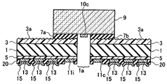
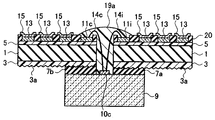
본 발명의 실시예와 관련된 반도체 장치는, 도 1에 나타내듯이, 제1 주표면 및 제2 주표면을 가지는 기판(1)과, 제1 주표면에 배치된 제1 접착제층(3)과, 제2 주표면에 배치된 제2 접착제층(5)과, 제1 접착제층(3)에 접착된 2개의 제3 접착제층(7a, 7b)과, 제3 접착제층(7a, 7b)에 접착된 반도체 칩(9)과, 반도체 칩(9)을 밀봉하는 밀봉 수지(제2 밀봉 수지)(19)를 구비한다. 여기서 「제1 주표면」이란, 실질적으로 평판 형상인 기판(1)의 한편의 주표면(면적이 최대 혹은 2 번째로 큰 면)을 가리킨다. 「제2 주표면」은, 기판(1)의 「제1 주표면」에 대향한 주표면을 가리킨다. 즉, 제l 및 제2 주표면의 어느쪽이든 한편이 「표면」, 다른 한편이 「이면」 이라고 해석할 수 있는 관계에 있는 대향한 2개의 면을 정의하고 있다.As shown in FIG. 1, a semiconductor device according to an embodiment of the present invention includes a
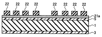
기판(1)은, 예를 들면 폴리이미드 수지로 된 수지 테이프 등이 채용 가능하다. 기판(1)의 반도체 칩(9)이 탑재되는 영역에는, 제1 주표면 및 제2 주표면 간을 관통하는 직사각형의 개구부(la)가 배치되어 있다. 도 1의 단면도에는 미크로인 표면 구조를 나타내지 않지만, 기판(1)의 제l 주표면 및 제2 주표면은, 각각 표면에 100 nm~5㎛ 정도의 작은 요철 형상을 갖는 요철 형상의 층이 형성되어 있다. 제l 접착제층(3) 및 제2 접착제층(5)은, 요철 형상의 층의 존재에 의해 야금성(冶金性)이 향상된 제1 주표면 및 제2 주표면에 각각 밀착되어 배치되어 있다.As the board |
제1 접착제층(3) 및 제2 접착제층(5)은, 기판(1)에 동박(Cu) 혹은 알루미늄 박(Al)등을 접착하기 위한 금속박용 접착제가 채용 가능하다. 제1 접착제층(3) 및 제2 접착제층(5)은, 에폭시계 수지 또는 폴리아라미드계 수지로부터 형성되는 것이 가능하여, 기판(1) 상에 막두께 5~20㎛ 정도로 형성되어 있다. 특히, 제1 접착제층(3)은, 기판(1) 또는 제3 접착제층(7a, 7b)과의 접착 강도 등을 고려하면 두껍게 형성되는 것이 바람직하지만, 너무 두껍게 형성되면 반도체 장치 전체의 두께가 증대한다. 한편, 제1 접착제층(3)을 너무 얇게 형성하면, 실장시에 보이드(void)가 발생한다. 이 때문에 , 제1 접착제층(3)의 막 두께는 10~15㎛, 더욱 바람직하게는 막 두께가 12㎛인 것이 좋다.The 1st
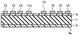
제3 접착제층(7a, 7b)은, 각각 에폭시계 수지 또는 실리콘계 수지 등의 반도체 칩 탑재용의 접착제로서, 제l 접착제층(3) 또는 제2 접착제층(5)에 비해 부드러운 재질의 접착제를 채용하는 것이 가능하다. 도 1의 단면도에 나타낸 바와 같이, 좌측의 제3 접착제층(7a)의 좌측의 단부는 탑재한 반도체 칩(9)의 좌측의 단부에 일치하도록 외형이 정의되어 있다. 우측의 제3 접착제층(7b)의 우측의 단부는 탑재하는 반도체 칩(9)의 우측의 단부에 일치하도록 외형이 정의되어 있다. 또, 제3 접착제층(7a, 7b)은, 각각 막 두께 25~100㎛ 정도로 형성되어 있다. 대향하는 2 개의 제3 접착제층(7a, 7b)은, 중앙부에 반도체 칩(9)의 칩측 본딩 패드(lOa, lOb, 10c,…, 10f)를 배치하기 위한 개구부를 가지도록 칩측 본딩 패드(lOa, lOb, 10c, …, 10f)를 서로 사이에 두는 위치에 형성되어 있다. 후술하는 도 13의 평면도 및 도 14의 단면도는, 제3 접착제층(7a, 7b)이 기판(1)에 형성된 직사각형의 개구부 (1a)를 사이에 두도록 개구부(1a)가 서로 마주 보는 2변을 따라 각각의 형상대로 배치된 상태를 나타내고 있다. 제3 접착제층(7a. 7b)의 각각의 막 두께는, 제l 접착제층(3) 및 반도체 칩(9)에의 접착 강도를 고려하면, 두껍게 형성되는 것이 바람직하지만, 너무 두껍게 형성하면 반도체 장치 전체의 두께가 증대한다. 한편, 제3 접착제층(7a, 7b)을 너무 얇게 형성하면 보이드가 발생한다. 제1 접착제층(3) 및 반도체칩(9)에의 야금성을 고려하면, 제3 접착제층(7a, 7b)의 막 두께는 40~75㎛, 더욱 바람직하게는 막 두께 50㎛인 것이 좋다.The third
제3 접착제층(7a, 7b)에 접착된 반도체 칩(9)은, 도 1에 나타낸 바와 같이, 소자면(9a)를 구비하여, 상기 소자면(9a)의 일부가 개구부(1a)로부터 노출되도록 기판(1) 위에 페이스다운방식으로 탑재되어 있다. 복수의 칩측 본딩 패드(lOa, lOb, 10c, …, 10f)는, 도 2에 나타낸 바와 같이, 개구부(1a)에 노출된 소자면(9a)의 중앙에 열(column)모양으로 배치되고, 금선(Au) 등으로 된 본딩선(14a, 14b, l4c, …, 14f)에 의해 각각 제2 주표면측의 우측의 기판측 본딩 패드(11a, l1b, 11c, …, 11f)에 접속되어 있다. 또, 칩측 본딩 패드(lOa, lOb, 10c,…, 10f)는, 금선(Au) 등으로 된 본딩선(14g, 14h, 14i, …, 14l)에 의해 각각 제2 주표면측의 좌측의 기판측 본딩 패드(11g, 11h, 11i, …, 11l)에 접속되어 있다.As shown in FIG. 1, the
제2 접착제층(5)에 접착된 복수의 전극(13)은, 기판(1)의 주변부, 즉 도 2 에 나타낸 바와 같이, 제2 주표면의 기판측 본딩 패드(11a, 11b, 11c,…, 11f)가 형성된 개구부(1a)의 우측의 잔여 영역 및 기판측 본딩 패드(11g, 11h, 11i, …, 11l)이 형성된 개구부(1a)의 좌측의 잔여 영역에 각각 어레이 형상으로 형성되어 있다. 또, 도 1에 나타낸 바와 같이, 기판측 본딩 패드(11a, 11b, 11c, …, 11f, …) 및 전극(13)의 주위에는, 솔더레지스터(20)가 배치되어 있다. 솔더레지스터(20)는, 기판측 본딩 패드(11) 및 전극(13)이 형성된 장소의 표면의 일부가 선택적으로 노출되도록 배치되어 있으며, 노출된 표면에는 니켈(Ni) 또는 금(Au) 등을 포함한 도금층(15)이 각각 배치되어 있다. 도금층(15)에는, 예를 들어 납(Pb)을 포함하지 않는, 이른바 무납(Pb-free) 반전 재료로 된 반전 볼(17)을 각각 접속하는 것이, 환경 문제면으로는 바람직하다.The plurality of
밀봉 수지(19)는, 개구부(1a)를 밀봉하는 제1 밀봉 수지(19a) 및 반도체 칩(9)을 밀봉하는 제2 밀봉 수지(19b)를 포함한다. 제1 밀봉 수지(19a)는, 소자면(9a), 칩측 본딩 패드(lOa, lOb, 10c, …, 10f), 기판측 본딩 패드(11a, 11b, 11c, …, 11f,…) 및 본딩선(14a, 14b, 14c, … , 14f, …) 주위를 덮도록, 제2 주표면측의 개구부(1a)를 메워 배치되어 있다. 제2 밀봉 수지(19b)는, 제1 접착제층(3)의 표면, 제3 접착제층(7a, 7b)의 측면, 반도체 칩(9)의 측면 및 표면에 각각 밀착하도록 배치되어 있다. 제l 밀봉 수지(19a) 및 제2 밀봉 수지(19b)로서는, 에폭시 수지, 실리콘 수지, 페놀 수지 등이 채용 가능하다.The sealing
본 발명의 실시예에 따른 반도체 장치는, 기판(1)과, 제3 접착제층(7a, 7b)과의 사이에, 금속박용 접착제로 된 제1 접착제층(3)이 배치된다. 이 때문에, 밀착 강도가 약하여 박리되기 쉬운 기판(1)과 제2 밀봉 수지(19b)는 직접 접촉하지 않기 때문에, 기판(1)과 제2 밀봉 수지(19b)간의 접촉면에 있어서의 박리를 방지할 수 있다. 또, 제3 접착제층(7a, 7b)은, 제1 접착제층(3) 상의 전면에 배치되는 것 이 아니라, 탑재하는 반도체 칩(9)의 외형에 맞춰 배치되므로, 접착 강도가 약하여 박리가 생기기 쉬운 제3 접착제층(7a. 7b)과 제2 밀봉 수지(19b)와의 접촉 면적을 최소로 할 수 있다. 따라서, 제2 밀봉 수지(19b)와 기판(1) 간의 박리가 되기 어렵게 할 수가 있다. 제1 접착제층(3)은, 표면에 요철 형상의 층이 형성된 기판(1)에 밀착해 배치되고 있으므로, 기판(1)과 제1 접착제층(3)과의 밀착 강도도 높고, 박리가 생기기 어렵다. 도 1에 나타낸 반도체 장치는, 반도체 칩(9)의 주위가 제2 밀봉 수지(19b)에 의해 밀봉되어 있기 때문에, 반도체 칩(9)의 크기가 반도체 장치 전체의 크기에 비해 현저하고 작은 경우에 대해서도, 기판(1)의 평탄성을 확보하는 것이 가능하며, 신뢰성 높은 반도체 장치를 제공할 수 있다.In the semiconductor device according to the embodiment of the present invention, a first
다음에, 본 발명의 실시예에 따른 반도체 장치의 실장 방법을 설명한다. 또한, 이하에 기술되는 반도체 장치의 실장 방법은 일 실시예이며, 이 실시예를 포함해, 이외의 여러 가지의 실장 방법에 의해 실현 가능함은 물론이다.Next, a method of mounting a semiconductor device according to an embodiment of the present invention will be described. In addition, the mounting method of the semiconductor device described below is an example, and can be realized by various mounting methods other than this including this example.
(i) 우선, 기판(1)으로서, 릴 형상의 폴리이미드 수지 등으로 된 수지 테이프를 준비한다. 그 기판(1)을 플라즈마 처리 장치 내에 넣어, 압력 12 Pa, 아르곤(Ar) 가스 유량 5m1/min, 투입 전력 250W의 프로세스 조건으로 10 초간 정도, Ar 플라즈마에 쬐어, 제1 주표면에 수 nm 정도의 요철 형상의 층을 형성한다. 제2 주표면도 플라즈마 처리에 의해 같은 요철 형상의 층을 형성한다. 이어서, 도 3에 나타낸 바와 같이, 기판(1)의 제1 주표면 및 제2 주표면의 전면에 제1 접착제층(3) 및 제2 접착제층(5)을 롤러 등을 이용해 형성한다. 다음에, 도 4에 나타낸 바와 같이, 제2 접착제층(5)의 표면에 Cu 또는 Al 등으로 되는 금속박(21a)을 덧붙인다. 그리고, 도 5에 나타낸 바와 같이, 금속박(21a)의 표면에 포토레지스트(photoresist)막(22)을 도포한다.(i) First, a resin tape made of a reel-shaped polyimide resin or the like is prepared as the
(ⅱ) 다음에, 도 6에 나타낸 바와 같이, 포토리소그래피(photolithography) 기술을 이용해 포토레지스트(photoresist)막(22)을 패터닝한다. 그리고, 패터닝 된 포토레지스트(photoresist)막(22)을 에칭 마스크로서, 반응성 이온 에칭(RIE) 등에 의해 금속박(21a)의 일부를 선택적으로 제거한 후, 도 7에 나타낸 바와 같이, 반도체 칩(9) 접속용의 기판측 본딩 패드(11c, …, 11i, …) 및 외부 단자 접속용의 전극(13)을 형성한다.(Ii) Next, as shown in FIG. 6, the
(ⅲ) 다음에, 스크린 인쇄 기술을 이용해 솔더레지스터(20)를 기판측 본딩 패드(11c, …, 11i, …) 및 전극(13)이 존재하는 표면에 각각 개구부(도시하지 않음)를 가지도록 도포한다. 그 후, 도 8에 나타낸 바와 같이, 스퍼터링 등에 의해 전극(13) 위에 Ni 또는 Au 등의 복수의 층으로 된 도금층(15)을 선택적으로 형성한다. 다음에, 도 9에 나타낸 바와 같이, 제1 접착제층(3)의 전면에 제3 접착제층(7a, 7b)을 형성한다.(Iii) Next, the solder resist 20 is formed to have openings (not shown) on the surface on which the substrate-
(ⅳ) 다음에, 도 10의 단면도 및 도 11의 평면도에 나타낸 바와 같이, 기판(1)의 개구부(1a)로 되는 영역 X의 양측으로 2개의 제3 접착제층(7a, 7b)이 각각 남도록, 제3 접착제층(7)의 일부를 선택적으로 구멍뚫어, 제거한다. 도 12의 단면도 및 도 13의 평면도에 나타낸 바와 같이, 기판(1)의 제1 주표면 및 제2 주표면을 관통하는 개구부(1a)를 형성한다. 또한, 제3 접착제층(7a, 7b)은, 미리 각각의 형상으로 성형해 제1 접착제층(3) 위에 직접 붙여도 좋다.(Iii) Next, as shown in the cross-sectional view of FIG. 10 and the top view of FIG. 11, two third
(v) 다음에, 도 14에 나타낸 바와 같이, 반도체 칩(9)의 소자면(9a)에 형성된 칩측 본딩 패드(10c, …)가 개구부(1a)의 제2 주표면측에 노출되도록, 반도체 칩(9)을 제3 접착제층(7a, 7b)의 위에 접착한다. 이 때, 제3 접착제층(7a)과 제3 접착제층(7b)이 구성하는 직사각형의 외형을, 반도체 칩(9)의 외형과 같은 크기에 패터닝 해 두면, 반도체 칩(9)의 외형은 제3 접착제층(7a, 7b)의 외형에 따르게 된다. 계속되어, 도 15에 나타낸 바와 같이, 기판(1)의 제2 주표면측에 형성된 기판측 본딩 패드(11c, …, 11i, …)와 반도체 칩(9)의 소자면(9a)에 형성된 칩측 본딩 패드(10c, …)를 열압착법 혹은 초음파 본딩법 등을 이용해 본딩선(14c, …, 14i, …)에 의해 접속한다.(v) Next, as shown in FIG. 14, the semiconductor such that the chip
(ⅵ) 이어서, 도 16에 나타내는 바와 같이, 칩측 본딩 패드(10c, …), 기판측 본딩 패드(l1c, …, 11i, …) 및 본딩선(14c, … , 14i, …) 주위에, 본딩 장치 등을 이용해 제l 밀봉 수지(19a)를 흘려 넣는다. 또한, 도 17에 나타낸 바와 같이, 몰드 장치 등을 이용해 반도체 칩(9)의 주위에 제2 밀봉 수지(19b)를 흘려 넣는다. 제1 밀봉 수지(19a) 및 제2 밀봉 수지(19b)는, 방치 또는 가열하여 경화시킨다. 그 후, 도금층의 표면에 플럭스(flux)를 도포하여, 도 18에 나타낸 바와 같이, 전극(13) 위에 반전 볼(17)을 각각 형성한다.(Iii) Next, as shown in FIG. 16, the bonding is performed around the chip
이상의 공정에 의해, 도 1에 나타내는 반도체 장치가 제조 가능해진다. 본 발명의 실시의 형태에 관계된 반도체 장치의 실장 방법에 의하면, 플라즈마 처리 등의 전처리를 수행하는 것에 의해 표면을 요철 형상을 가지도록 한 기판(1)의 제1 주표면에 제1 접착제층(3)을 형성하므로, 기판(1)과 제1 접착제층(3) 간의 밀착 강 도가 향상된다. 또, 제3 접착제층(7a, 7b)을 제l 접착제층(3)의 표면 전면에 형성하는 것이 아니라, 반도체 칩(9)의 외형에 따르도록 반도체 칩(9)이 탑재되는 장소에만 선택적으로 배치되므로, 밀착 강도가 약한 제3 접착제층(7a, 7b)과 제2 밀봉 수지(19b) 간의 접촉면을 작게 할 수 있고, 박리를 생기기 어렵게 할 수가 있다. 한층 더, 기판(1)과 제2 밀봉 수지(19b)와의 사이에 제1 접착제층(3)을 배치하는 것에 의해, 밀착 강도가 약한 기판(1)과 제2 밀봉 수지(19b)가 직접 접착하지 않고, 밀착 강도의 향상을 꾀할 수 있다. 또, 반도체 칩(9)의 주위를 제2 밀봉 수지(19b)에 의해 밀봉하는 것에 의해, 기판(1)의 평탄성을 확보하는 것이 가능하며, 신뢰성 높은 반도체 장치를 제조하는 것이 가능하다.By the above process, the semiconductor device shown in FIG. 1 can be manufactured. According to the method for mounting a semiconductor device according to the embodiment of the present invention, the first
또한, 반도체 칩(9)의 주위를 제1 및 제2 밀봉 수지(19a, 19b)에 의해 밀봉하는 공정은, 도 19에 나타낸 바와 같이, 몰드 장치 등의 금형(23) 내에 기판(1) 을 넣고, 개구부(1a) 및 반도체 칩(9)의 주변에 동시에 밀봉 수지(19)를 흘려 넣는 공정으로 할 수도 있다. 밀봉 수지(19)를 흘려 넣어, 수지를 경화시킨 후는, 도 20에 나타낸 바와 같이, 전극(13) 상에 반전 볼(17)을 각각 탑재하는 것에 의해, 도 1에 나타내는 반도체 장치가 제조 가능해진다.In addition, the process of sealing the circumference | surroundings of the
(다른 실시예)(Other embodiment)
본 발명의 다른 실시예와 관련된 반도체 장치는, 도 21에 나타낸 바와 같이, 제1 접착제층(3)의 제3 접착제층(7a, 7b)에 접촉하는 측의 표면에 요철 형상의 층인 앵커(anchor)부(3a)가 형성되고 있다. 「앵커부(3a)」는, 제1 접착제층(3)의 제 3 접착제층(7)에 접촉하는 측의 표면에 금속박을 형성해, 금속박을 박리하는 것에 의해 형성된 약 0.1~5㎛의 높이의 요철면을 가지는 층이다. 그 외는, 도 1에 나타내는 반도체 장치와 동일하기 때문에, 중복 기재를 생략한다. 도 21에 나타내는 반도체 장치에 의하면, 제l 접착제층(3)의 표면에 요철 형상을 가지는 앵커부(3a)가 배치되므로, 제1 접착제층(3)으로 접촉하는 제3 접착제층(7a, 7b) 혹은 제2 밀봉 수지(19b)와의 접착성이 향상된다. 또, 반도체 칩(9)의 주위가 제2 밀봉 수지(19b)에 의해 밀봉되므로, 반도체 칩(9)의 크기가 탑재하는 기판(1)에 대해서 현저히 작은 경우에 대해서도 기판(1)의 평탄성을 확보하는 것이 가능하며, 신뢰성 높은 반도체 장치를 제공할 수 있다.In the semiconductor device according to another embodiment of the present invention, as shown in FIG. 21, the anchor is an uneven layer on the surface of the side of the first
다음에, 도 21에 나타내는 반도체 장치의 실장 방법을 설명한다. 또한, 이하에 기술되는 반도체 장치의 실장 방법은 일례이며, 이 실시예를 포함하여, 이외의 여러 가지의 실장 방법에 의해 실현 가능한 것은 물론이다.Next, the mounting method of the semiconductor device shown in FIG. 21 is demonstrated. In addition, the mounting method of the semiconductor device described below is an example, Of course, it can be realized by various mounting methods other than this Example.
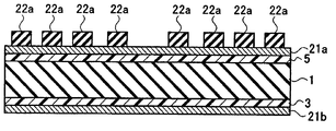
(i) 기판(1)으로서, 릴 형상의 폴리이미드 수지 등으로 된 수지 테이프를 준비한다. 상기 기판(1)을 플라즈마 처리 장치 내에 넣어, 압력 12 Pa, 아르곤(Ar) 가스 유량 5ml/min, 투입 전력 250W의 프로세스 조건으로 10 초간 정도, 기판(1)을 Ar 플라즈마에 쬐어, 제1 주표면에 도 1에 나타내는 구조의 제조 방법과 같은 요철면을 가지는 층을 형성한다. 제2 주표면에도 플라즈마 처리에 의해 제l 주표면과 같은 요철면을 가지는 층을 형성한다. 계속되어, 도 22에 나타낸 바와 같이, 기판(1)의 제l 주표면 및 제2 주표면의 전면에 제1 접착제층(3) 및 제2 접착제층(5)을 롤러 등에 의해 형성한다. 다음에, 도 23에 나타낸 바와 같이, 제1 접착제층(3) 위에 Cu 혹은 Al 등으로 된 금속박(21b)을, 제2 접착제층(5) 위에 Cu 혹은 Al 등으로 된 금속박(21a)을 각각 형성한다. 한층 더, 도 24에 나타낸 바와 같이, 금속박(21a)의 표면에 포토레지스트(photoresist)막(22a)을 각각 도포한다.(i) As the board |
(ⅱ) 다음으로, 도 25에 나타낸 바와 같이, 포토리소그래피 기술을 이용해 포토레지스트(photoresist)막(22a)를 패터닝한다. 그리고, 패터닝된 포토레지스트(photoresist)막(22a)를 에칭 마스크로서, RIE 등에 의해 금속박(21a)을 선택적으로 제거한다. 또한, 제l 접착제층(3) 상에 형성된 금속박(21b)을 RIE 등에 의해 벗겨낸다. 이 결과, 도 26에 나타낸 바와 같이, 제2 접착제층(5) 상에는 기판측 본딩패드(11c, …, 11i, …) 및 전극(13)이 형성된다. 제l 접착제층(3) 상에는, 요철의 층인 앵커부(3a)가 형성된다.(Ii) Next, as shown in FIG. 25, the
(ⅲ) 다음으로, 스크린 인쇄 기술을 이용해 솔더레지스터(20)를 기판측 본딩 패드(11c, …, 11i, …) 및 전극(13)이 노출되도록 도포한다. 그 후, 도 27에 나타낸 바와 같이, 전극(13) 위에 Ni 또는 Au 등의 복수의 층으로 된 도금층을 각각 스퍼터링 등에 의해 형성한다. 그리고, 도 28에 나타낸 바와 같이, 표면에 앵커부 (3a)가 형성된 제1 접착제층(3)의 전면에 제3 접착제층(7a, 7b)을 형성한다.(Iv) Next, the
(ⅳ) 다음으로, 도 29에 나타낸 바와 같이, 기판(1)의 개구부(1a)가 되는 영역(X)의 양측으로 제3 접착제층(7a, 7b)이 선택적으로 잔존하도록, 제3 접착제층(7a, 7b)의 일부를 선택적으로 구멍뚫어 제거한다. 도 30에 나타낸 바와 같이, 기판(1)의 제l 주표면 및 제2 주표면을 관통하는 개구부(1a)를 형성한다. 또한, 제3 접착제층(7a, 7b)은, 미리 각각의 형태별로 성형해 제1 접착제층(3) 위에 직접 붙 여도 좋다.(Iv) Next, as shown in FIG. 29, the 3rd adhesive bond layer so that 3rd
(v) 다음으로, 도 31에 나타낸 바와 같이, 반도체 칩(9)의 소자면(9a)의 일부가 개구부(1a)의 제2 주표면측에 노출되도록, 반도체 칩(9)을 제3 접착제층(7a, 7b) 위에 탑재한다. 이 때, 제3 접착제층(7a, 7b)의 외형을 반도체 칩(9)의 외형과 같은 크기에 패터닝해 두면, 반도체 칩(9)의 외형은, 제3 접착제층(7a)과 제3 접착제층(7b)이 구성하는 직사각형의 외형에 따르게 된다. 계속하여, 도 32에 나타낸 바와 같이, 기판(1)의 제2 주표면측에 형성된 기판측 본딩 패드(l1c, …, 11i, …)와 반도체 칩(9)의 소자면(9a)에 형성된 칩측 본딩 패드(10c, …)를 열압착법 또는 초음파 본딩법 등을 이용해 본딩선(14c, …, 14i, …)에 의해 접속한다.(v) Next, as shown in FIG. 31, the
(ⅵ) 이어서, 도 33에 나타낸 바와 같이, 칩측 본딩 패드(10c, …)와, 본딩선(14c, …, 14i, …) 주위에, 포팅(potting) 장치 등을 이용해 제l 밀봉 수지(19a)를 흘려 넣는다. 또한, 도 34에 나타낸 바와 같이, 몰드 장치 등을 이용해 반도체 칩(9)의 주위를 제2 밀봉 수지(19b)로 밀봉한다. 제1 밀봉 수지(19a) 및 제2 밀봉 수지(19b)는, 방치 또는 가열해 경화시킨다. 그 후, 도금층(15)의 표면에 플럭스를 도포해, 도 35에 나타낸 바와 같이, 전극(13) 위에 반전 볼(17)을 각각 형성한다.(Iii) Subsequently, as shown in FIG. 33, around the chip
이상의 공정에 의해, 도 21에 나타내는 반도체 장치가 제조 가능해진다. 도 21에 나타내는 반도체장치의 실장 방법에 의하면, 플라즈마 처리에 의해 표면에 요철 형상의 층이 형성된 기판(1)의 제l 주표면에 제l 접착제층(3)을 형성하므로, 기판(1)과 제l 접착제층(3)과의 밀착 강도가 향상된다. 또한, 제1 접착제층(3)은, 제3 접착제층(7a, 7b)에 접착하는 측의 표면에 금속박(21b)을 형성해, 금속박(21b)을 벗겨내는 것에 의해 표면에 요철면을 가지는 앵커부(3a)를 형성하므로, 제1 접착제층(3) 표면의 야금성이 향상된다. 이 때문에, 제1 접착제층(3)으로 접촉하는 제3 접착제층(7a, 7b) 및 제2 밀봉 수지(19b)와의 접착 강도가 향상되어, 신뢰성 높은 반도체 장치를 제조할 수 있다. 또, 제3 접착제층(7a, 7b)은, 제1 접착제층(3) 표면의 반도체 칩(9)이 탑재되는 장소에만 선택적으로 형성하는 것에 의해, 접착 강도가 약한 제3 접착제층(7a, 7b)과 제2 밀봉 수지(19b)와의 접촉 면적을 최소한으로 억제하는 것이 가능하며, 박리가 생기기 어렵게 할 수가 있다. 또, 반도체 칩(9)의 주위를 제2 밀봉 수지(19b)에 의해 밀봉하는 것에 의해, 기판(1)의 평탄성을 확보할 수 있으므로, 신뢰성 높은 반도체 장치가 제조 가능하다.Through the above steps, the semiconductor device shown in FIG. 21 can be manufactured. According to the semiconductor device mounting method shown in FIG. 21, since the 1st
(접착 강도의 평가)(Evaluation of Adhesive Strength)
도 1 및 도 21에 나타내는 반도체 장치의 접착 강도를 평가하기 위해서, 필(peel) 시험을 실시했다. 구체적으로는, 도 36에 나타낸 바와 같이, 필 시험 평가용의 베이스 기판이 되는 유리 에폭시 기판(31)의 일면에 도 1 혹은 도 21에 나타내는 제3 접착제층(7a, 7b)과 같은 재료로 되는 에폭시계 또는 실리콘계의 칩 접착용의 접착제(32)를 배치한다. 이 접착제(32) 위에, 측정 기판(33)의 인장 강도를 측정하고 싶은 쪽의 면(측정면)을 접착시킨다. 또한, 측정 기판(33)의 다른 일면(비측정면)에 대해 수직 방향(도 17의 화살표 방향)으로 접어 구부린 벤딩(bending)부(34a)를 가지는 동박(34)을, 측정 기판(33) 위에 붙인다. 상기 벤딩부(34a)를 수직 방향으로 인장하는 것으로 접착 강도를 평가했다. 필 시험에 의한 박리 상태 (파괴 모드)는, 도 37에 나타낸 바와 같이, 동박(34)으로 측정 기판(33)의 피측정면과의 계면에 있어서의 박리를 「A 모드 」, 측정 기판(33) 내의 박리를 「B 모드 」, 측정 기판(33)과 접착제(32)와의 계면에 있어서의 박리를 「C 모드 」라고 부른다.In order to evaluate the adhesive strength of the semiconductor device shown in FIG. 1 and FIG. 21, the peel test was implemented. Specifically, as shown in FIG. 36, one surface of the
측정 시료의 측정 기판(33)에는, 앞서 실시예에 관해 설명한 폴리이미드로 된 수지 테이프 기판을 사용했다. 도 38에 나타내는 「실시예 1」은, 폴리이미드로 된 측정 기판(33)의 측정면에 도 l에 나타내는 제1 접착제층(3)과 같은 재질 및 막 두께의 동박용 접착제를 배치해, 이 측정면을 접착제(32)에 접착시켜 도 36에 나타내는 필 시험을 실시한 결과를 나타낸다. 「실시예 2」는, 측정면에 도 21에 나타내는 앵커부(3a)와 같은 재질 및 막 두께의 요철 형상의 층을 형성해, 이 측정면을 접착제(32)에 접착시켜 도 36에 나타내는 필 시험을 실시한 결과를 나타낸다. 「비교예」는, 측정 기판(33)의 측정면에 도 1 및 도 21에 나타내는 제1 접착제층(3)을 배치하지 않고 직접, 측정 기판(33)과 도 36에 나타내는 접착제(32)를 접착시킨 예를 나타낸다. 또한, 도 38중의 「무처리」란, 기판(1)의 표면에 전 처리를 실시하지 않는 기판을 나타내며, 「전처리」란, 기판(1)의 표면을 아르곤 플라즈마에 의해 미리 전처리한 기판을 나타낸다.As the measurement board |
도 38에 나타내는 그래프로부터 분명하게, 측정 기판(33)의 측정면에 제1 접착제층(3)을 가지지 않는 기판인 「비교예」는, 플라즈마 처리 등의 전처리의 유무에 관련되지 않고 인장강도가 O.7~0.9 N/cm 정도이며, 충분한 접착 강도는 얻지 못하고 있다. 또, 파괴 모드는 「c 모드」이며, 칩 접착용의 접착제(32)와 측정 기 판(33)의 계면에서 박리가 생기고 있다. 한편, 기판 표면에 제1 접착제층(3)을 갖는 「실시예 1」의 경우는, 기판 표면에 요철 형상의 층을 가지도록 전처리를 수행하는 것에 의해 인장 강도가 7.9~13.4 N/cm정도까지 증대한다. 또한, 제1 접착제층(3)의 표면에 앵커부(3a)가 형성된 「실시예 2」의 경우는, 인장 강도가 16 N/cm 이상 (측정 불능)이 되어, 개질(改質) 처리의 유무에 관계없이 강한 접착 강도를 얻을 수 있음을 알 수 있다. 또, 파괴 모드도 「A 모드」이며, 접착제(32)와 측정 기판(33)과의 계면에 있어서의 박리도 생기지 않고, 비교예에 비해 현저하게 접착 강도가 증대되어 있는 것을 알 수 있다. 이 결과로부터, 도 1 또는 도 21에 나타내는 반도체 장치와 같이, 기판(1)의 제1 주표면에 제1 접착제층(3)을 배치해, 제l 접착제층(3)에 앵커부(3a)를 형성하는 것에 의해, 반도체 칩(9)의 크기가 현저히 작은 BGA에 대해서도 기판(1)의 주위에 배치되는 밀봉 수지(19) 또는 접착제층(제3 접착제층(7a, 7b))과의 접착 강도를 높게 유지할 수 있는 것을 알 수 있다.Clearly from the graph shown in FIG. 38, the "comparative example" which is a board | substrate which does not have the 1st
(그 외의 실시예)(Other Examples)
상기와 같이, 본 발명은 실시예를 기재하였으나, 상기 명시된 일부를 이루는 기재 및 도면이 이 발명을 한정하는 것이라고 이해해서는 안된다. 당업자가 본 발명의 기재로부터 여러가지 대체적 실시 형태, 실시예 및 운용기술을 생각해 낼 수 있음은 명백하다.As described above, the present invention has been described in the examples, but it should not be understood that the description and drawings which form part of the above-mentioned limit the present invention. It will be apparent to those skilled in the art that various alternative embodiments, examples and operational techniques may be devised from the description of the invention.
도 1에 나타낸 반도체 장치의 칩측 본딩 패드(10c, …)는, 반드시 반도체 칩(9)의 중앙부에 배치될 필요는 없고, 반도체 칩(9)의 단부에 배치할 수도 있다. 예를 들면, 도 39 및 도 40에 나타낸 바와 같이, 반도체 칩(9A)의 단부 2 개소에 복수의 칩측 본딩 패드(lOA, lOB)가 존재하는 경우는, 기판(1)에 2 개소의 개구부(1A, 1B)를 형성하여, 개구부(1A, 1B)로부터 각각 칩측 본딩 패드(10A, lOB)가 노출되도록 반도체 칩(9)을 배치해, 칩측 본딩 패드(10A, lOB)의 주위를 밀봉 수지(19A, 19B)에 의해 밀봉하는 형태도 채용 가능하다.The chip
또한, 도 1 및 도 21에 나타낸 바와 같이, 제3 접착제층(3a, 3b)은, 기판(1) 의 개구부(la)의 양단을 사이에 두도록 각각 떨어뜨려 배치하는 것만이 아니고, 개구부(1a)의 주위 전체를 둘러싸도록, 한 장의 접착제층으로서 형성해도 좋은 것은 물론이다.In addition, as shown to FIG. 1 and FIG. 21, the 3rd
이와 같이, 본 발명은 본 명세서에 기재하고 있지 않은 여러가지 실시의 형태등을 포함하는 것은 물론이다. 따라서, 본 발명의 기술적 범위는 상기의 설명으로부터 타당한 특허 청구의 범위와 관련되는 발명 특정 사항에 의해서만 정해질 수 있는 것이다.Thus, of course, this invention includes various embodiment etc. which are not described in this specification. Accordingly, the technical scope of the present invention can be determined only by the invention specific matters related to the claims which are appropriate from the above description.
본 발명에 의하면, 기판과 밀봉 수지와의 밀착성을 향상시킨 신뢰성 높은 반도체 장치 및 그 실장 방법을 제공할 수 있다.According to the present invention, a highly reliable semiconductor device having improved adhesion between the substrate and the sealing resin and a mounting method thereof can be provided.
Claims (5)
Applications Claiming Priority (2)
| Application Number | Priority Date | Filing Date | Title |
|---|---|---|---|
| JPJP-P-2004-00256022 | 2004-09-02 | ||
| JP2004256022A JP2006073825A (en) | 2004-09-02 | 2004-09-02 | Semiconductor device and mounting method thereof |
Publications (2)
| Publication Number | Publication Date |
|---|---|
| KR20060050880A KR20060050880A (en) | 2006-05-19 |
| KR100676386B1 true KR100676386B1 (en) | 2007-01-30 |
Family
ID=36033053
Family Applications (1)
| Application Number | Title | Priority Date | Filing Date |
|---|---|---|---|
| KR1020050080776A Expired - Fee Related KR100676386B1 (en) | 2004-09-02 | 2005-08-31 | Semiconductor device and mounting method thereof |
Country Status (3)
| Country | Link |
|---|---|
| US (1) | US7298035B2 (en) |
| JP (1) | JP2006073825A (en) |
| KR (1) | KR100676386B1 (en) |
Families Citing this family (21)
| Publication number | Priority date | Publication date | Assignee | Title |
|---|---|---|---|---|
| JP5329083B2 (en) * | 2004-06-25 | 2013-10-30 | テッセラ,インコーポレイテッド | Parts with posts and pads |
| JP2006339317A (en) * | 2005-05-31 | 2006-12-14 | Toshiba Corp | Surface mount semiconductor device |
| KR100713931B1 (en) * | 2006-03-29 | 2007-05-07 | 주식회사 하이닉스반도체 | High speed and high performance semiconductor packages |
| KR100800148B1 (en) * | 2006-06-30 | 2008-02-01 | 주식회사 하이닉스반도체 | FWA Package |
| KR100780693B1 (en) * | 2006-06-30 | 2007-11-30 | 주식회사 하이닉스반도체 | FWA Package |
| US7901989B2 (en) | 2006-10-10 | 2011-03-08 | Tessera, Inc. | Reconstituted wafer level stacking |
| US8513789B2 (en) | 2006-10-10 | 2013-08-20 | Tessera, Inc. | Edge connect wafer level stacking with leads extending along edges |
| US7829438B2 (en) | 2006-10-10 | 2010-11-09 | Tessera, Inc. | Edge connect wafer level stacking |
| US7759166B2 (en) * | 2006-10-17 | 2010-07-20 | Tessera, Inc. | Microelectronic packages fabricated at the wafer level and methods therefor |
| US7759807B2 (en) * | 2006-11-21 | 2010-07-20 | Hynix Semiconductor Inc. | Semiconductor package having structure for warpage prevention |
| US7952195B2 (en) | 2006-12-28 | 2011-05-31 | Tessera, Inc. | Stacked packages with bridging traces |
| JP4550073B2 (en) * | 2007-01-18 | 2010-09-22 | 力成科技股▲分▼有限公司 | IC chip package structure |
| KR101458538B1 (en) | 2007-07-27 | 2014-11-07 | 테세라, 인코포레이티드 | A stacked microelectronic unit, and method of fabrication thereof |
| US8551815B2 (en) | 2007-08-03 | 2013-10-08 | Tessera, Inc. | Stack packages using reconstituted wafers |
| US8043895B2 (en) | 2007-08-09 | 2011-10-25 | Tessera, Inc. | Method of fabricating stacked assembly including plurality of stacked microelectronic elements |
| TWI365517B (en) * | 2008-05-23 | 2012-06-01 | Unimicron Technology Corp | Circuit structure and manufactring method thereof |
| CN102067310B (en) | 2008-06-16 | 2013-08-21 | 泰塞拉公司 | Stacking of wafer-level chip scale packages having edge contacts and manufacture method thereof |
| JP4845952B2 (en) * | 2008-11-10 | 2011-12-28 | 力成科技股▲分▼有限公司 | Window type semiconductor package |
| CN102422412A (en) | 2009-03-13 | 2012-04-18 | 德塞拉股份有限公司 | Stacked microelectronic assemblies having vias extending through bond pads |
| KR101078741B1 (en) * | 2009-12-31 | 2011-11-02 | 주식회사 하이닉스반도체 | Semiconductor package and stacked semiconductor package having thereof |
| EP2884242B1 (en) | 2013-12-12 | 2021-12-08 | ams International AG | Sensor Package And Manufacturing Method |
Family Cites Families (12)
| Publication number | Priority date | Publication date | Assignee | Title |
|---|---|---|---|---|
| JPS63155732A (en) * | 1986-12-19 | 1988-06-28 | Agency Of Ind Science & Technol | Semiconductor device |
| JPH02127092A (en) * | 1988-11-08 | 1990-05-15 | Hitachi Maxell Ltd | Ic card module |
| JPH04123441A (en) * | 1990-09-14 | 1992-04-23 | Hitachi Ltd | Semiconductor integrated circuit device |
| JP4505769B2 (en) * | 2000-03-31 | 2010-07-21 | 日立化成工業株式会社 | Adhesive film, wiring board for semiconductor mounting provided with adhesive film, semiconductor device, and manufacturing method thereof |
| JP2001358253A (en) * | 2000-06-12 | 2001-12-26 | Hitachi Cable Ltd | BGA type semiconductor device |
| JP2002040095A (en) * | 2000-07-26 | 2002-02-06 | Nec Corp | Semiconductor device and mounting method thereof |
| JP2002198458A (en) * | 2000-12-26 | 2002-07-12 | Nec Corp | Semiconductor device and semiconductor device manufacturing method |
| JP2002208656A (en) * | 2001-01-11 | 2002-07-26 | Mitsubishi Electric Corp | Semiconductor device |
| JP3651413B2 (en) * | 2001-05-21 | 2005-05-25 | 日立電線株式会社 | Semiconductor device tape carrier, semiconductor device using the same, semiconductor device tape carrier manufacturing method, and semiconductor device manufacturing method |
| US7323772B2 (en) * | 2002-08-28 | 2008-01-29 | Micron Technology, Inc. | Ball grid array structures and tape-based method of manufacturing same |
| JP3883543B2 (en) * | 2003-04-16 | 2007-02-21 | 新光電気工業株式会社 | Conductor substrate and semiconductor device |
| US7061085B2 (en) * | 2003-09-19 | 2006-06-13 | Micron Technology, Inc. | Semiconductor component and system having stiffener and circuit decal |
-
2004
- 2004-09-02 JP JP2004256022A patent/JP2006073825A/en active Pending
-
2005
- 2005-08-31 KR KR1020050080776A patent/KR100676386B1/en not_active Expired - Fee Related
- 2005-09-01 US US11/216,144 patent/US7298035B2/en not_active Expired - Fee Related
Also Published As
| Publication number | Publication date |
|---|---|
| US7298035B2 (en) | 2007-11-20 |
| JP2006073825A (en) | 2006-03-16 |
| US20060055061A1 (en) | 2006-03-16 |
| KR20060050880A (en) | 2006-05-19 |
Similar Documents
| Publication | Publication Date | Title |
|---|---|---|
| KR100676386B1 (en) | Semiconductor device and mounting method thereof | |
| JP2825083B2 (en) | Semiconductor element mounting structure | |
| JP3400877B2 (en) | Semiconductor device and manufacturing method thereof | |
| CN101410973B (en) | Wafer level chip scale package and methods of making and using same | |
| JP5018826B2 (en) | Electronic device and manufacturing method thereof | |
| US6794739B2 (en) | Semiconductor device, process for production thereof, and electronic equipment | |
| CN101288351B (en) | Printed wiring board and method for manufacturing printed wiring board | |
| US7749806B2 (en) | Fabricating process of a chip package structure | |
| JPH10178145A (en) | Semiconductor device, manufacturing method thereof, and insulating substrate for semiconductor device | |
| KR100315138B1 (en) | Semiconductor device and its manufacturing method and film carrier tape and its manufacturing method | |
| US6271057B1 (en) | Method of making semiconductor chip package | |
| CN100466237C (en) | Semiconductor device, substrate for manufacturing semiconductor device, and method for manufacturing same | |
| JPH053183A (en) | Semiconductor device and manufacturing method thereof | |
| JP3956903B2 (en) | Semiconductor module, electronic device, and method for manufacturing semiconductor module | |
| JP2001127117A (en) | Method for manufacturing TAB tape | |
| KR100432136B1 (en) | Chip scale package and fabrication method thereof | |
| EP1365450A1 (en) | An improved wire-bonded chip on board package | |
| CN1442891A (en) | Soft package structure and manufacturing method thereof | |
| US20030205793A1 (en) | Wire-bonded chip on board package | |
| JPS5940539A (en) | Manufacture of semiconductor device | |
| JP3449097B2 (en) | Semiconductor device | |
| JPH1140697A (en) | Tape carrier for semiconductor device | |
| JPH02234449A (en) | Semiconductor device | |
| JPH0397237A (en) | Connection of tab tape and semiconductor chip and bump sheet therefor | |
| JP2000269266A (en) | Semiconductor package manufacturing method |
Legal Events
| Date | Code | Title | Description |
|---|---|---|---|
| A201 | Request for examination | ||
| PA0109 | Patent application |
St.27 status event code: A-0-1-A10-A12-nap-PA0109 |
|
| PA0201 | Request for examination |
St.27 status event code: A-1-2-D10-D11-exm-PA0201 |
|
| PG1501 | Laying open of application |
St.27 status event code: A-1-1-Q10-Q12-nap-PG1501 |
|
| E701 | Decision to grant or registration of patent right | ||
| PE0701 | Decision of registration |
St.27 status event code: A-1-2-D10-D22-exm-PE0701 |
|
| GRNT | Written decision to grant | ||
| PR0701 | Registration of establishment |
St.27 status event code: A-2-4-F10-F11-exm-PR0701 |
|
| PR1002 | Payment of registration fee |
St.27 status event code: A-2-2-U10-U11-oth-PR1002 Fee payment year number: 1 |
|
| PG1601 | Publication of registration |
St.27 status event code: A-4-4-Q10-Q13-nap-PG1601 |
|
| PR1001 | Payment of annual fee |
St.27 status event code: A-4-4-U10-U11-oth-PR1001 Fee payment year number: 4 |
|
| PR1001 | Payment of annual fee |
St.27 status event code: A-4-4-U10-U11-oth-PR1001 Fee payment year number: 5 |
|
| FPAY | Annual fee payment |
Payment date: 20120105 Year of fee payment: 6 |
|
| PR1001 | Payment of annual fee |
St.27 status event code: A-4-4-U10-U11-oth-PR1001 Fee payment year number: 6 |
|
| LAPS | Lapse due to unpaid annual fee | ||
| PC1903 | Unpaid annual fee |
St.27 status event code: A-4-4-U10-U13-oth-PC1903 Not in force date: 20130125 Payment event data comment text: Termination Category : DEFAULT_OF_REGISTRATION_FEE |
|
| PC1903 | Unpaid annual fee |
St.27 status event code: N-4-6-H10-H13-oth-PC1903 Ip right cessation event data comment text: Termination Category : DEFAULT_OF_REGISTRATION_FEE Not in force date: 20130125 |
|
| R18 | Changes to party contact information recorded |
Free format text: ST27 STATUS EVENT CODE: A-5-5-R10-R18-OTH-X000 (AS PROVIDED BY THE NATIONAL OFFICE) |
|
| R18-X000 | Changes to party contact information recorded |
St.27 status event code: A-5-5-R10-R18-oth-X000 |
|
| P22-X000 | Classification modified |
St.27 status event code: A-4-4-P10-P22-nap-X000 |