CN102067310B - Stacking of wafer-level chip scale packages having edge contacts and manufacture method thereof - Google Patents
Stacking of wafer-level chip scale packages having edge contacts and manufacture method thereof Download PDFInfo
- Publication number
- CN102067310B CN102067310B CN2009801225230A CN200980122523A CN102067310B CN 102067310 B CN102067310 B CN 102067310B CN 2009801225230 A CN2009801225230 A CN 2009801225230A CN 200980122523 A CN200980122523 A CN 200980122523A CN 102067310 B CN102067310 B CN 102067310B
- Authority
- CN
- China
- Prior art keywords
- microelectronic
- microelectronic device
- conductive
- edge
- conductive element
- Prior art date
- Legal status (The legal status is an assumption and is not a legal conclusion. Google has not performed a legal analysis and makes no representation as to the accuracy of the status listed.)
- Active
Links
Images


Classifications
-
- H—ELECTRICITY
- H10—SEMICONDUCTOR DEVICES; ELECTRIC SOLID-STATE DEVICES NOT OTHERWISE PROVIDED FOR
- H10W—GENERIC PACKAGES, INTERCONNECTIONS, CONNECTORS OR OTHER CONSTRUCTIONAL DETAILS OF DEVICES COVERED BY CLASS H10
- H10W90/00—Package configurations
-
- H—ELECTRICITY
- H10—SEMICONDUCTOR DEVICES; ELECTRIC SOLID-STATE DEVICES NOT OTHERWISE PROVIDED FOR
- H10W—GENERIC PACKAGES, INTERCONNECTIONS, CONNECTORS OR OTHER CONSTRUCTIONAL DETAILS OF DEVICES COVERED BY CLASS H10
- H10W72/00—Interconnections or connectors in packages
-
- H—ELECTRICITY
- H10—SEMICONDUCTOR DEVICES; ELECTRIC SOLID-STATE DEVICES NOT OTHERWISE PROVIDED FOR
- H10D—INORGANIC ELECTRIC SEMICONDUCTOR DEVICES
- H10D62/00—Semiconductor bodies, or regions thereof, of devices having potential barriers
- H10D62/10—Shapes, relative sizes or dispositions of the regions of the semiconductor bodies; Shapes of the semiconductor bodies
- H10D62/117—Shapes of semiconductor bodies
-
- H—ELECTRICITY
- H10—SEMICONDUCTOR DEVICES; ELECTRIC SOLID-STATE DEVICES NOT OTHERWISE PROVIDED FOR
- H10W—GENERIC PACKAGES, INTERCONNECTIONS, CONNECTORS OR OTHER CONSTRUCTIONAL DETAILS OF DEVICES COVERED BY CLASS H10
- H10W74/00—Encapsulations, e.g. protective coatings
- H10W74/10—Encapsulations, e.g. protective coatings characterised by their shape or disposition
- H10W74/111—Encapsulations, e.g. protective coatings characterised by their shape or disposition the semiconductor body being completely enclosed
- H10W74/129—Encapsulations, e.g. protective coatings characterised by their shape or disposition the semiconductor body being completely enclosed forming a chip-scale package [CSP]
-
- H—ELECTRICITY
- H10—SEMICONDUCTOR DEVICES; ELECTRIC SOLID-STATE DEVICES NOT OTHERWISE PROVIDED FOR
- H10W—GENERIC PACKAGES, INTERCONNECTIONS, CONNECTORS OR OTHER CONSTRUCTIONAL DETAILS OF DEVICES COVERED BY CLASS H10
- H10W70/00—Package substrates; Interposers; Redistribution layers [RDL]
- H10W70/01—Manufacture or treatment
- H10W70/05—Manufacture or treatment of insulating or insulated package substrates, or of interposers, or of redistribution layers
- H10W70/093—Connecting or disconnecting other interconnections thereto or therefrom, e.g. connecting bond wires or bumps
-
- H—ELECTRICITY
- H10—SEMICONDUCTOR DEVICES; ELECTRIC SOLID-STATE DEVICES NOT OTHERWISE PROVIDED FOR
- H10W—GENERIC PACKAGES, INTERCONNECTIONS, CONNECTORS OR OTHER CONSTRUCTIONAL DETAILS OF DEVICES COVERED BY CLASS H10
- H10W70/00—Package substrates; Interposers; Redistribution layers [RDL]
- H10W70/099—Connecting interconnections to insulating or insulated package substrates, interposers or redistribution layers
-
- H—ELECTRICITY
- H10—SEMICONDUCTOR DEVICES; ELECTRIC SOLID-STATE DEVICES NOT OTHERWISE PROVIDED FOR
- H10W—GENERIC PACKAGES, INTERCONNECTIONS, CONNECTORS OR OTHER CONSTRUCTIONAL DETAILS OF DEVICES COVERED BY CLASS H10
- H10W70/00—Package substrates; Interposers; Redistribution layers [RDL]
- H10W70/60—Insulating or insulated package substrates; Interposers; Redistribution layers
- H10W70/62—Insulating or insulated package substrates; Interposers; Redistribution layers characterised by their interconnections
- H10W70/65—Shapes or dispositions of interconnections
- H10W70/652—Cross-sectional shapes
- H10W70/6523—Cross-sectional shapes for connecting to pads at different heights at the same side of the package substrate, interposer or RDL
-
- H—ELECTRICITY
- H10—SEMICONDUCTOR DEVICES; ELECTRIC SOLID-STATE DEVICES NOT OTHERWISE PROVIDED FOR
- H10W—GENERIC PACKAGES, INTERCONNECTIONS, CONNECTORS OR OTHER CONSTRUCTIONAL DETAILS OF DEVICES COVERED BY CLASS H10
- H10W70/00—Package substrates; Interposers; Redistribution layers [RDL]
- H10W70/60—Insulating or insulated package substrates; Interposers; Redistribution layers
- H10W70/62—Insulating or insulated package substrates; Interposers; Redistribution layers characterised by their interconnections
- H10W70/65—Shapes or dispositions of interconnections
- H10W70/652—Cross-sectional shapes
- H10W70/6528—Cross-sectional shapes of the portions that connect to chips, wafers or package parts
-
- H—ELECTRICITY
- H10—SEMICONDUCTOR DEVICES; ELECTRIC SOLID-STATE DEVICES NOT OTHERWISE PROVIDED FOR
- H10W—GENERIC PACKAGES, INTERCONNECTIONS, CONNECTORS OR OTHER CONSTRUCTIONAL DETAILS OF DEVICES COVERED BY CLASS H10
- H10W70/00—Package substrates; Interposers; Redistribution layers [RDL]
- H10W70/60—Insulating or insulated package substrates; Interposers; Redistribution layers
- H10W70/62—Insulating or insulated package substrates; Interposers; Redistribution layers characterised by their interconnections
- H10W70/65—Shapes or dispositions of interconnections
- H10W70/654—Top-view layouts
-
- H—ELECTRICITY
- H10—SEMICONDUCTOR DEVICES; ELECTRIC SOLID-STATE DEVICES NOT OTHERWISE PROVIDED FOR
- H10W—GENERIC PACKAGES, INTERCONNECTIONS, CONNECTORS OR OTHER CONSTRUCTIONAL DETAILS OF DEVICES COVERED BY CLASS H10
- H10W72/00—Interconnections or connectors in packages
- H10W72/01—Manufacture or treatment
- H10W72/019—Manufacture or treatment of bond pads
- H10W72/01904—Manufacture or treatment of bond pads using temporary auxiliary members, e.g. using sacrificial coatings or handle substrates
-
- H—ELECTRICITY
- H10—SEMICONDUCTOR DEVICES; ELECTRIC SOLID-STATE DEVICES NOT OTHERWISE PROVIDED FOR
- H10W—GENERIC PACKAGES, INTERCONNECTIONS, CONNECTORS OR OTHER CONSTRUCTIONAL DETAILS OF DEVICES COVERED BY CLASS H10
- H10W72/00—Interconnections or connectors in packages
- H10W72/01—Manufacture or treatment
- H10W72/0198—Manufacture or treatment batch processes
-
- H—ELECTRICITY
- H10—SEMICONDUCTOR DEVICES; ELECTRIC SOLID-STATE DEVICES NOT OTHERWISE PROVIDED FOR
- H10W—GENERIC PACKAGES, INTERCONNECTIONS, CONNECTORS OR OTHER CONSTRUCTIONAL DETAILS OF DEVICES COVERED BY CLASS H10
- H10W72/00—Interconnections or connectors in packages
- H10W72/071—Connecting or disconnecting
- H10W72/073—Connecting or disconnecting of die-attach connectors
-
- H—ELECTRICITY
- H10—SEMICONDUCTOR DEVICES; ELECTRIC SOLID-STATE DEVICES NOT OTHERWISE PROVIDED FOR
- H10W—GENERIC PACKAGES, INTERCONNECTIONS, CONNECTORS OR OTHER CONSTRUCTIONAL DETAILS OF DEVICES COVERED BY CLASS H10
- H10W72/00—Interconnections or connectors in packages
- H10W72/20—Bump connectors, e.g. solder bumps or copper pillars; Dummy bumps; Thermal bumps
- H10W72/29—Bond pads specially adapted therefor
-
- H—ELECTRICITY
- H10—SEMICONDUCTOR DEVICES; ELECTRIC SOLID-STATE DEVICES NOT OTHERWISE PROVIDED FOR
- H10W—GENERIC PACKAGES, INTERCONNECTIONS, CONNECTORS OR OTHER CONSTRUCTIONAL DETAILS OF DEVICES COVERED BY CLASS H10
- H10W72/00—Interconnections or connectors in packages
- H10W72/30—Die-attach connectors
- H10W72/351—Materials of die-attach connectors
- H10W72/353—Materials of die-attach connectors not comprising solid metals or solid metalloids, e.g. ceramics
- H10W72/354—Materials of die-attach connectors not comprising solid metals or solid metalloids, e.g. ceramics comprising polymers
-
- H—ELECTRICITY
- H10—SEMICONDUCTOR DEVICES; ELECTRIC SOLID-STATE DEVICES NOT OTHERWISE PROVIDED FOR
- H10W—GENERIC PACKAGES, INTERCONNECTIONS, CONNECTORS OR OTHER CONSTRUCTIONAL DETAILS OF DEVICES COVERED BY CLASS H10
- H10W72/00—Interconnections or connectors in packages
- H10W72/801—Interconnections on sidewalls of containers
-
- H—ELECTRICITY
- H10—SEMICONDUCTOR DEVICES; ELECTRIC SOLID-STATE DEVICES NOT OTHERWISE PROVIDED FOR
- H10W—GENERIC PACKAGES, INTERCONNECTIONS, CONNECTORS OR OTHER CONSTRUCTIONAL DETAILS OF DEVICES COVERED BY CLASS H10
- H10W72/00—Interconnections or connectors in packages
- H10W72/834—Interconnections on sidewalls of chips
-
- H—ELECTRICITY
- H10—SEMICONDUCTOR DEVICES; ELECTRIC SOLID-STATE DEVICES NOT OTHERWISE PROVIDED FOR
- H10W—GENERIC PACKAGES, INTERCONNECTIONS, CONNECTORS OR OTHER CONSTRUCTIONAL DETAILS OF DEVICES COVERED BY CLASS H10
- H10W72/00—Interconnections or connectors in packages
- H10W72/851—Dispositions of multiple connectors or interconnections
- H10W72/874—On different surfaces
-
- H—ELECTRICITY
- H10—SEMICONDUCTOR DEVICES; ELECTRIC SOLID-STATE DEVICES NOT OTHERWISE PROVIDED FOR
- H10W—GENERIC PACKAGES, INTERCONNECTIONS, CONNECTORS OR OTHER CONSTRUCTIONAL DETAILS OF DEVICES COVERED BY CLASS H10
- H10W72/00—Interconnections or connectors in packages
- H10W72/90—Bond pads, in general
- H10W72/921—Structures or relative sizes of bond pads
- H10W72/922—Bond pads being integral with underlying chip-level interconnections
-
- H—ELECTRICITY
- H10—SEMICONDUCTOR DEVICES; ELECTRIC SOLID-STATE DEVICES NOT OTHERWISE PROVIDED FOR
- H10W—GENERIC PACKAGES, INTERCONNECTIONS, CONNECTORS OR OTHER CONSTRUCTIONAL DETAILS OF DEVICES COVERED BY CLASS H10
- H10W72/00—Interconnections or connectors in packages
- H10W72/90—Bond pads, in general
- H10W72/931—Shapes of bond pads
- H10W72/934—Cross-sectional shape, i.e. in side view
-
- H—ELECTRICITY
- H10—SEMICONDUCTOR DEVICES; ELECTRIC SOLID-STATE DEVICES NOT OTHERWISE PROVIDED FOR
- H10W—GENERIC PACKAGES, INTERCONNECTIONS, CONNECTORS OR OTHER CONSTRUCTIONAL DETAILS OF DEVICES COVERED BY CLASS H10
- H10W72/00—Interconnections or connectors in packages
- H10W72/90—Bond pads, in general
- H10W72/941—Dispositions of bond pads
- H10W72/944—Dispositions of multiple bond pads
- H10W72/9445—Top-view layouts, e.g. mirror arrays
-
- H—ELECTRICITY
- H10—SEMICONDUCTOR DEVICES; ELECTRIC SOLID-STATE DEVICES NOT OTHERWISE PROVIDED FOR
- H10W—GENERIC PACKAGES, INTERCONNECTIONS, CONNECTORS OR OTHER CONSTRUCTIONAL DETAILS OF DEVICES COVERED BY CLASS H10
- H10W80/00—Direct bonding of chips, wafers or substrates
- H10W80/701—Direct bonding of chips, wafers or substrates characterised by the pads after the direct bonding
- H10W80/743—Direct bonding of chips, wafers or substrates characterised by the pads after the direct bonding having disposition changed during the connecting
-
- H—ELECTRICITY
- H10—SEMICONDUCTOR DEVICES; ELECTRIC SOLID-STATE DEVICES NOT OTHERWISE PROVIDED FOR
- H10W—GENERIC PACKAGES, INTERCONNECTIONS, CONNECTORS OR OTHER CONSTRUCTIONAL DETAILS OF DEVICES COVERED BY CLASS H10
- H10W90/00—Package configurations
- H10W90/20—Configurations of stacked chips
-
- H—ELECTRICITY
- H10—SEMICONDUCTOR DEVICES; ELECTRIC SOLID-STATE DEVICES NOT OTHERWISE PROVIDED FOR
- H10W—GENERIC PACKAGES, INTERCONNECTIONS, CONNECTORS OR OTHER CONSTRUCTIONAL DETAILS OF DEVICES COVERED BY CLASS H10
- H10W90/00—Package configurations
- H10W90/20—Configurations of stacked chips
- H10W90/22—Configurations of stacked chips the stacked chips being on both top and bottom sides of a package substrate, interposer or RDL
-
- H—ELECTRICITY
- H10—SEMICONDUCTOR DEVICES; ELECTRIC SOLID-STATE DEVICES NOT OTHERWISE PROVIDED FOR
- H10W—GENERIC PACKAGES, INTERCONNECTIONS, CONNECTORS OR OTHER CONSTRUCTIONAL DETAILS OF DEVICES COVERED BY CLASS H10
- H10W90/00—Package configurations
- H10W90/20—Configurations of stacked chips
- H10W90/271—Configurations of stacked chips the chips having passive surfaces facing each other, i.e. in a back-to-back arrangement
-
- H—ELECTRICITY
- H10—SEMICONDUCTOR DEVICES; ELECTRIC SOLID-STATE DEVICES NOT OTHERWISE PROVIDED FOR
- H10W—GENERIC PACKAGES, INTERCONNECTIONS, CONNECTORS OR OTHER CONSTRUCTIONAL DETAILS OF DEVICES COVERED BY CLASS H10
- H10W90/00—Package configurations
- H10W90/701—Package configurations characterised by the relative positions of pads or connectors relative to package parts
- H10W90/721—Package configurations characterised by the relative positions of pads or connectors relative to package parts of bump connectors
- H10W90/722—Package configurations characterised by the relative positions of pads or connectors relative to package parts of bump connectors between stacked chips
-
- H—ELECTRICITY
- H10—SEMICONDUCTOR DEVICES; ELECTRIC SOLID-STATE DEVICES NOT OTHERWISE PROVIDED FOR
- H10W—GENERIC PACKAGES, INTERCONNECTIONS, CONNECTORS OR OTHER CONSTRUCTIONAL DETAILS OF DEVICES COVERED BY CLASS H10
- H10W90/00—Package configurations
- H10W90/701—Package configurations characterised by the relative positions of pads or connectors relative to package parts
- H10W90/731—Package configurations characterised by the relative positions of pads or connectors relative to package parts of die-attach connectors
- H10W90/732—Package configurations characterised by the relative positions of pads or connectors relative to package parts of die-attach connectors between stacked chips
-
- H—ELECTRICITY
- H10—SEMICONDUCTOR DEVICES; ELECTRIC SOLID-STATE DEVICES NOT OTHERWISE PROVIDED FOR
- H10W—GENERIC PACKAGES, INTERCONNECTIONS, CONNECTORS OR OTHER CONSTRUCTIONAL DETAILS OF DEVICES COVERED BY CLASS H10
- H10W90/00—Package configurations
- H10W90/701—Package configurations characterised by the relative positions of pads or connectors relative to package parts
- H10W90/791—Package configurations characterised by the relative positions of pads or connectors relative to package parts of direct-bonded pads
- H10W90/792—Package configurations characterised by the relative positions of pads or connectors relative to package parts of direct-bonded pads between multiple chips
-
- Y—GENERAL TAGGING OF NEW TECHNOLOGICAL DEVELOPMENTS; GENERAL TAGGING OF CROSS-SECTIONAL TECHNOLOGIES SPANNING OVER SEVERAL SECTIONS OF THE IPC; TECHNICAL SUBJECTS COVERED BY FORMER USPC CROSS-REFERENCE ART COLLECTIONS [XRACs] AND DIGESTS
- Y10—TECHNICAL SUBJECTS COVERED BY FORMER USPC
- Y10T—TECHNICAL SUBJECTS COVERED BY FORMER US CLASSIFICATION
- Y10T29/00—Metal working
- Y10T29/49—Method of mechanical manufacture
- Y10T29/49002—Electrical device making
- Y10T29/49117—Conductor or circuit manufacturing
- Y10T29/49124—On flat or curved insulated base, e.g., printed circuit, etc.
- Y10T29/4913—Assembling to base an electrical component, e.g., capacitor, etc.
- Y10T29/49144—Assembling to base an electrical component, e.g., capacitor, etc. by metal fusion
Landscapes
- Wire Bonding (AREA)
- Internal Circuitry In Semiconductor Integrated Circuit Devices (AREA)
Abstract
Description
相关申请的交叉引用Cross References to Related Applications
本申请要求2008年6月16日提交的美国临时专利申请61/061953的优先权,其公开内容在此引用作为参考。 This application claims priority to US Provisional Patent Application 61/061953, filed June 16, 2008, the disclosure of which is incorporated herein by reference. the
技术领域 technical field
本发明涉及封装的微电子元件及其制造方法,并且更特别地涉及可堆叠的被封装微电子模板组件。 The present invention relates to packaged microelectronic components and methods of making the same, and more particularly to stackable packaged microelectronic template assemblies. the
背景技术 Background technique
微电子芯片典型地为带有反向相对、基本平坦的前表面和后表面且带有在这些表面之间延伸的边缘的平板体。芯片通常在前表面上具有与芯片内的电路电连接的触头,有时也称为垫或结合垫。典型地通过用适宜材料包围芯片来封装芯片,以形成具有电接于芯片触头的端子的微电子封装。接着封装被连接于测试设备以确定已封装装置是否符合所需的性能标准。一旦被测试,通过借助适宜的连接方法如焊接将封装端子连接于印刷电路板(PCB)上的匹配焊盘(lands),封装可被连接于较大的电路如电子产品如计算机或手机的电路。 Microelectronic chips are typically planar bodies with opposed, substantially planar front and rear surfaces with edges extending between these surfaces. Chips typically have contacts, sometimes called pads or bond pads, on the front surface that electrically connect circuits within the chip. The chip is typically packaged by surrounding the chip with a suitable material to form a microelectronic package having terminals electrically connected to the chip's contacts. The package is then connected to test equipment to determine whether the packaged device meets the required performance criteria. Once tested, the package can be connected to a larger circuit such as that of an electronic product such as a computer or cell phone by connecting the package terminals to mating lands on a printed circuit board (PCB) by suitable connection methods such as soldering . the
微电子封装可以晶片级被制造;也就是说,构成封装的外壳、终端和其它结构被制造的同时芯片或模板仍然为晶片形式。形成模板之后,对晶片进行多个额外加工步骤以形成晶片上的封装结构,接着晶片被切块以分离各个已封装模板。晶片级加工是优选的制造方法,因为它可提供节约成本的优点,且因为可使得每个模板封装的覆盖区(footprint)与模板自身的尺寸相同或几乎相同,这就能够非常有效地利用已封装模板要被连接到的印刷电路板上的区域。以这种方式封装的模板一般称为晶片级芯片规模封装或晶片级芯片尺寸封装(WLCSP)。 Microelectronic packages can be fabricated at the wafer level; that is, the housing, terminals, and other structures that make up the package are fabricated while the chip or template remains in wafer form. After the templates are formed, the wafer is subjected to a number of additional processing steps to form packaged structures on the wafer, and the wafer is then diced to separate the individual packaged templates. Wafer-level processing is the preferred manufacturing method because it offers cost-saving advantages and because the footprint of each stencil package can be made to be the same or nearly the same size as the stencil itself, which allows very efficient use of existing The area on the printed circuit board to which the package template is to be attached. Stencils packaged in this manner are generally referred to as wafer-level chip-scale packaging or wafer-level chip-scale packaging (WLCSP). the
为节约封装模板安装于其的基板上的额外空间,可通过竖直堆叠多个 芯片来将多个芯片合并为单独的封装。叠层中的每个模板必须典型地为叠层中的一个或多个其它模板,或叠层安装于其上的基板,或皆为两者提供电连接机构。这就使得竖直堆叠的多个模板封装在基板上占用的表面积小于封装内所有芯片加起来的总表面积。因为当使用模板叠层时比封装单个模板时通常具有多得多的电连接,叠层中不同模板之间的电连接必须极其稳定和可靠。 To save additional space on the substrate to which the package template is mounted, multiple chips can be combined into a single package by stacking them vertically. Each die in the stack must typically provide electrical connection mechanisms to one or more other dies in the stack, or the substrate on which the stack is mounted, or both. This allows vertically stacked multiple stencil packages to occupy less surface area on the substrate than the combined total surface area of all chips within the package. Because there are typically many more electrical connections when using a die stack than when packaging a single die, the electrical connections between the different dies in the stack must be extremely stable and reliable. the
发明内容 Contents of the invention
一种微电子组件可包括第一微电子装置和第二微电子装置。每个微电子装置都包括带有至少一个半导体模板的模板结构,并且每个微电子装置具有第一表面、远离该第一表面的第二表面和以除直角外的角度延伸离开第一和第二表面的至少一个边缘表面。至少一个导电元件沿第一表面延伸至所述边缘表面的至少之一之上和第二表面之上。该第一微电子装置的至少一个导电元件导电地结合于该第二微电子装置的至少一个导电元件从而在其间提供导电路径。 A microelectronic assembly may include a first microelectronic device and a second microelectronic device. Each microelectronic device includes a template structure with at least one semiconductor template, and each microelectronic device has a first surface, a second surface remote from the first surface and extending away from the first and second surfaces at an angle other than a right angle. At least one edge surface of the two surfaces. At least one conductive element extends along the first surface onto at least one of the edge surfaces and onto the second surface. At least one conductive element of the first microelectronic device is conductively bonded to at least one conductive element of the second microelectronic device to provide a conductive path therebetween. the
根据一个实施例,每个微电子装置的导电元件可包括通过镀覆到第一和第二表面之一上形成的第一元件以及通过镀覆到第一和第二表面中另一个和所述至少一个边缘表面上而形成的第二元件。在一个实施例中,第二元件被镀覆在第一元件的一些部分上。例如,第二元件沿第二元件在其上被镀覆的第一元件的这些部分延伸。 According to one embodiment, the conductive elements of each microelectronic device may include a first element formed by plating onto one of the first and second surfaces and a first element formed by plating onto the other of the first and second surfaces and the A second element is formed on at least one edge surface. In one embodiment, the second element is plated on portions of the first element. For example, the second element extends along those portions of the first element on which the second element is plated. the
第二元件能沿第一元件的边缘延伸从而在这些边缘处与第一元件导电地接合。 The second element can extend along the edges of the first element to electrically conductively engage the first element at these edges. the
例如能使用可熔性金属或使用导电膏结合第一和第二微电子装置的导电元件。在一个实施例中,第一微电子装置的第一和第二表面之一能面对第二微电子装置的第一和第二表面之一并且导电元件的暴露于相面对表面处的部分被结合在一起。例如,导电元件可包括暴露于每个微电子装置的第一或第二表面的至少之一处的导电垫并且所述各导电垫能被结合在一起。 For example a fusible metal can be used or a conductive paste can be used to bond the conductive elements of the first and second microelectronic devices. In one embodiment, one of the first and second surfaces of the first microelectronic device can face one of the first and second surfaces of the second microelectronic device and the portion of the conductive element exposed at the facing surface are combined. For example, the conductive elements can include conductive pads exposed at at least one of the first or second surfaces of each microelectronic device and the conductive pads can be bonded together. the
导电元件可包括迹线和导电垫,其中至少一个导电垫与至少一个边缘面间隔开而设置。在一个特定实施例中,每个微电子装置的导电元件包括 紧挨所述至少一个边缘表面或能延伸至所述至少一个边缘表面的导电垫。 The conductive element may include traces and conductive pads, wherein at least one conductive pad is spaced apart from the at least one edge face. In a particular embodiment, the conductive elements of each microelectronic device include conductive pads proximate to or extending to said at least one edge surface. the
在一个特定实施例中,一个或多个微电子装置能包括多个模板。在这种情形下,包括在所述至少一个微电子装置内的至少两个半导体模板的结合垫-承载表面朝着同一方向,或它们可朝着不同方向。 In a particular embodiment, one or more microelectronic devices can include multiple templates. In this case, the bonding pad-carrying surfaces of at least two semiconductor templates comprised in said at least one microelectronic device face the same direction, or they may face different directions. the
所述至少一个导电元件沿其延伸的所述至少一个边缘表面可相对第一和第二表面中至少之一以50~89度角设置。 The at least one edge surface along which the at least one conductive element extends may be disposed at an angle of 50 to 89 degrees relative to at least one of the first and second surfaces. the
在微电子组件中,第一和第二微电子装置以竖直方向被堆叠并且第一和第二微电子装置的所述至少一个边缘表面彼此偏移。 In the microelectronic assembly, the first and second microelectronic devices are stacked in a vertical orientation and the at least one edge surface of the first and second microelectronic devices are offset from each other. the
第一和第二微电子装置的第一表面能侧向(lateral)延伸且在侧向上具有第一尺寸。在一个实施例中,第一和第二微电子装置的第一表面的侧向尺寸可为不同的。 The first surfaces of the first and second microelectronic devices can extend laterally and have a first dimension in the lateral direction. In one embodiment, the lateral dimensions of the first surface of the first and second microelectronic devices may be different. the
在一个实施例中,提供了一种微电子组件,其包括第一微电子装置和第二微电子装置。每个微电子装置都能包括带有至少一个半导体模板的模板结构。每个微电子装置具有第一表面、远离该第一表面的第二表面和延伸离开第一表面的至少一个边缘表面。导电元件能沿第一表面延伸至所述边缘表面的至少之一上。该第一微电子装置的至少一个导电元件能导电地结合于该第二微电子装置的至少一个导电元件从而在其间提供导电路径。 In one embodiment, a microelectronic assembly is provided that includes a first microelectronic device and a second microelectronic device. Each microelectronic device can include a template structure with at least one semiconductor template. Each microelectronic device has a first surface, a second surface remote from the first surface, and at least one edge surface extending away from the first surface. The conductive element can extend along the first surface onto at least one of the edge surfaces. At least one conductive element of the first microelectronic device is conductively bonded to at least one conductive element of the second microelectronic device to provide a conductive path therebetween. the
在一个实施例中,所述至少一个边缘表面以除直角外的角度远离第一和第二表面延伸。导电元件的暴露于所述至少一个边缘表面处的边缘部分能被导电地结合以提供导电路径。能使用可熔性金属或使用导电膏结合所述边缘部分。 In one embodiment, said at least one edge surface extends away from the first and second surfaces at an angle other than a right angle. An edge portion of the conductive element exposed at the at least one edge surface can be conductively bonded to provide a conductive path. The edge portion can be bonded using a fusible metal or using a conductive paste. the
根据一个实施例提供了一种制造叠层微电子组件的方法。在该实施例中,第一微电子装置的主表面能被设置为与第二微电子装置的主表面相对。暴露于第一微电子装置的主表面处的导电元件能被导电地结合于暴露于第二微电子装置的主表面处的导电元件以提供其间的导电路径。每个微电子装置能包括带有至少一个半导体模板的模板结构,并且每个微电子装置能具有第一主表面、远离该第一表面的第二主表面、至少一个边缘表面、以及沿第一表面延伸至所述边缘表面的至少之一之上和第二主表面之上的至少一个导电元件。 According to one embodiment, a method of fabricating a stacked microelectronic assembly is provided. In this embodiment, a major surface of the first microelectronic device can be disposed opposite a major surface of the second microelectronic device. The conductive elements exposed at the major surface of the first microelectronic device can be conductively bonded to the conductive elements exposed at the major surface of the second microelectronic device to provide a conductive path therebetween. Each microelectronic device can include a template structure with at least one semiconductor template, and each microelectronic device can have a first major surface, a second major surface remote from the first surface, at least one edge surface, and The surface extends to at least one conductive element over at least one of the edge surfaces and over the second major surface. the
根据一个实施例,能制造一种堆叠的微电子组件。能形成包括第一微 电子装置和第二微电子装置的叠层。每个微电子装置都能包括带有至少一个半导体模板的模板结构。每个微电子装置能具有第一表面、远离该第一表面的第二表面和延伸离开第一表面的至少一个边缘表面。至少一个导电元件能沿第一表面延伸至所述边缘表面的至少之一之上。暴露于边缘表面处的导电元件的部分能被导电地结合从而在其间提供导电路径。 According to one embodiment, a stacked microelectronic assembly can be fabricated. A stack comprising the first microelectronic device and the second microelectronic device can be formed. Each microelectronic device can include a template structure with at least one semiconductor template. Each microelectronic device can have a first surface, a second surface remote from the first surface, and at least one edge surface extending away from the first surface. At least one conductive element can extend along the first surface onto at least one of the edge surfaces. Portions of the conductive elements exposed at the edge surfaces can be conductively bonded to provide a conductive path therebetween. the
在该实施例中,第一微电子装置能被置于第二微电子装置之上,并且通过加热暴露于第一微电子装置至少一个边缘表面处的导电元件附近的可熔性金属来进行结合步骤。这样可熔性金属流至暴露于第二微电子装置至少一个边缘表面处的导电元件之上。在该实施例中,可熔性金属桥接第一和第二微电子装置的导电元件之间的间隙。 In this embodiment, the first microelectronic device can be placed over the second microelectronic device and bonded by heating the fusible metal exposed near the conductive element at at least one edge surface of the first microelectronic device step. The fusible metal thus flows over the conductive element exposed at at least one edge surface of the second microelectronic device. In this embodiment, the fusible metal bridges the gap between the conductive elements of the first and second microelectronic devices. the
在该实施例中,第一微电子装置能设在第二微电子装置之上,并且通过将可流动导电材料配送至暴露于第一微电子装置至少一个边缘表面处的导电元件上来进行结合步骤。接着导电材料可流至暴露于第二微电子装置至少一个边缘表面处的导电元件之上。 In this embodiment, the first microelectronic device can be disposed over the second microelectronic device and the bonding step is performed by dispensing a flowable conductive material onto the conductive element exposed at at least one edge surface of the first microelectronic device . The conductive material can then flow over the conductive elements exposed at at least one edge surface of the second microelectronic device. the
附图说明 Description of drawings
在结合附图阅读了下面对多个实施例的描述时,能最好地理解此处描述的装置和方法,附图中相同的附图标记指的是相同或类似的部件。附图不一定是按比例绘制的;而是强调示出所示实施例的原理。 The apparatus and methods described herein are best understood from the following description of the various embodiments when read in conjunction with the accompanying drawings, in which like reference numbers refer to the same or like parts. The drawings are not necessarily to scale; emphasis instead being placed upon illustrating the principles of the illustrated embodiments. the
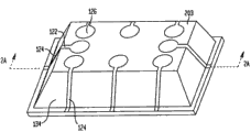
图1A示出含有多个微电子芯片的晶片的透视图。 Figure 1A shows a perspective view of a wafer containing a plurality of microelectronic chips. the
图1B示出晶片一部分的截面图。 Figure 1B shows a cross-sectional view of a portion of a wafer. the
图1C示出根据一个实施例具有设于结合垫上的第一金属化层的晶片的单个模板(die)的透视图。 Figure 1C shows a perspective view of a single die of a wafer with a first metallization layer disposed on bond pads according to one embodiment. the
图1D-1I示出经受了额外加工步骤的类似于图1B的晶片一部分的截面图。 1D-1I show cross-sectional views of a portion of a wafer similar to FIG. 1B that has undergone additional processing steps. the
图2A示出根据一个实施例的分离的微电子装置的截面图。 Figure 2A shows a cross-sectional view of an isolated microelectronic device according to one embodiment. the
图2B和2C示出根据一个实施例的图2A中接合结构的变型的详图。 2B and 2C show detailed views of variations of the engagement structure of FIG. 2A, according to one embodiment. the
图2D示出图2A的微电子装置的透视图。 Figure 2D shows a perspective view of the microelectronic device of Figure 2A. the
图2E概述了用于制造根据一个实施例的最终微电子装置的工艺流程图。 Figure 2E outlines a process flow diagram for fabricating a final microelectronic device according to one embodiment. the
图3示出根据一个实施例形成模板叠层结构的多个模板的截面图。 Figure 3 shows a cross-sectional view of a plurality of templates forming a template stack according to one embodiment. the
图4A和4B示出根据一个实施例形成图3装置的接合方法的两个变型的截面图。 4A and 4B show cross-sectional views of two variations of a bonding method to form the device of FIG. 3 according to one embodiment. the
图5A示出根据一个实施例包括不同元件的模板叠层结构的截面图。 Figure 5A shows a cross-sectional view of a template stack comprising different elements according to one embodiment. the
图5B示出根据一个实施例包括不同元件且模板尺寸各异的模板叠层结构的截面图。 Figure 5B shows a cross-sectional view of a template stack comprising different elements and varying template sizes according to one embodiment. the
图6A示出根据一个实施例具有设在结合垫上的第一金属化层的晶片的单个模板的透视图。 6A shows a perspective view of a single template of a wafer with a first metallization layer disposed on bond pads according to one embodiment. the
图6B示出根据一个实施例带有延伸至边缘的结合垫的晶片的单个模板的透视图。 6B shows a perspective view of a single template of a wafer with bond pads extending to the edge, according to one embodiment. the
图6C-6I示出根据一个实施例经受了额外加工步骤的晶片某部分的截面图,其模板类似于图6A的模板。 6C-6I show cross-sectional views of a portion of a wafer subjected to additional processing steps with a template similar to that of FIG. 6A, according to one embodiment. the
图7示出根据一个实施例形成的模板叠层结构的截面图。 Figure 7 shows a cross-sectional view of a template stack formed according to one embodiment. the
图8A示出根据一个实施例的模板结构的截面图。 Figure 8A shows a cross-sectional view of a template structure according to one embodiment. the
图8B示出根据一个实施例添加有额外的可回流材料的模板叠层的截面图。 Figure 8B shows a cross-sectional view of a stencil stack with additional reflowable material added according to one embodiment. the
图8C示出根据一个实施例的模板叠层结构的截面图。 Figure 8C shows a cross-sectional view of a template stack according to one embodiment. the
图9概述了根据一个实施例用于制造最终装置模板的工艺流程图。 Figure 9 outlines a process flow diagram for fabricating a final device template according to one embodiment. the
图10A-10E示出根据一个实施例导致形成包括两个或更多个模板的模板叠层的加工步骤的截面图。 10A-10E illustrate cross-sectional views of processing steps leading to the formation of a template stack comprising two or more templates, according to one embodiment. the
图10F示出根据一个实施例包括两个或更多个模板的模板结构的截面图。 Figure 10F shows a cross-sectional view of a template structure comprising two or more templates according to one embodiment. the
图10G示出根据一个实施例包括图10F的多个模板结构的模板叠层结构的截面图。 Figure 10G illustrates a cross-sectional view of a template stack structure comprising the plurality of template structures of Figure 10F, according to one embodiment. the
图10H示出根据一个实施例在图10A中开始的那部分工艺流程的变型的截面图。 Figure 10H shows a cross-sectional view of a variation of the portion of the process flow beginning in Figure 10A, according to one embodiment. the
图11A-11E示出根据一个实施例导致形成模板叠层的加工步骤的截面图。 11A-11E illustrate cross-sectional views of processing steps leading to the formation of a template stack according to one embodiment. the
图11F示出根据一个实施例包括两个或更多个模板的模板结构的截面图。 Figure 1 IF shows a cross-sectional view of a template structure comprising two or more templates according to one embodiment. the
图11G示出根据一个实施例包括图11F的多个模板结构的模板叠层结构的截面图。 FIG. 11G shows a cross-sectional view of a template stack structure comprising a plurality of template structures of FIG. 11F according to one embodiment. the
具体实施方式 Detailed ways
在本文中,导电结构“暴露在”绝缘体结构表面这样的陈述指的是导电结构可用于与以垂直于绝缘体结构表面的方向从绝缘体结构外侧朝绝缘体结构表面移动的理论点相接触。因此,暴露于绝缘体结构表面处的端子或其它导电结构可从该表面突出;可与该表面齐平;或可相对该表面凹陷且通过绝缘体内的孔或凹口被暴露。 In this context, the statement that the conductive structure is "exposed" on the surface of the insulator structure means that the conductive structure is available for contact with a theoretical point moving from the outside of the insulator structure towards the surface of the insulator structure in a direction perpendicular to the surface of the insulator structure. Thus, terminals or other conductive structures exposed at a surface of an insulator structure may protrude from the surface; may be flush with the surface; or may be recessed relative to the surface and exposed through holes or indentations within the insulator. the
图1A示出含有多个微电子芯片的晶片100的透视图。晶片基板102通常为半导体材料如硅,但也可由其它材料制成或为一些类型的复合材料。晶片被分割为包括微电子芯片的工作部分的部分或全部独立模板104;在额外加工后这些模板在虚线103处彼此分离。每个芯片可具有一种或更多功能且使用半导体加工的本领域技术人员公知的技术形成于基板表面的上面或下面。这些示例不作为限定——被加工的晶片100可代表各种类型的装置,包括存储器、处理器、图像传感器或其他可能性。结合垫106电接于基板之上或基板之内的电路。图1B示出晶片如图1A中示出的晶片100某部分的截面图。为清楚起见,结合垫106暴露于基板102的“前面”或接触支承面101上。结合垫106可从表面101上突起,可与该表面齐平或可相对该表面凹陷。虚线103表明每个模板之间的切割线。尽管所述的晶片可为带有形成于其内的工作部分的半导体材料,在其它情形下晶片也可为重组晶片,其中通过被设置为形成各独立模板且借助粘合剂如环氧树脂被保持在一起的多个构件来形成晶片。可选地,代替晶片100的是,该结构可以是多个模板,这些模板在如虚线103所示的其边缘处连接在一起,这种结构可为矩形如面板。这些模板的边缘可在虚线处相接并且半导体材料可为连续的未切割结构,或模板的边缘彼此隔开并且用粘合剂接合为重组结构。
FIG. 1A shows a perspective view of a
图1C-1I示出根据一个实施例加工晶片的步骤。要注意,所示步骤可采用所述顺序或可选地采用不同顺序进行。在某些实施例中,两个或更多个所述步骤可合并为一个步骤。在其它实施例中,可从工艺中完全取消一 个所述步骤。在其它变型中,可能需要额外的加工步骤。 1C-1I illustrate steps in processing a wafer according to one embodiment. It is to be noted that the steps shown may be performed in the order described or alternatively in a different order. In some embodiments, two or more of the described steps may be combined into one step. In other embodiments, one of the described steps can be completely eliminated from the process. In other variations, additional processing steps may be required. the
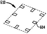
图1C为具有接触结合垫的第一金属化层110的晶片100的单个模板108的透视图。可采用某些方式如沉积或镀覆将金属膜沉积在晶片表面101上,接着膜被构图以形成金属化层。在特定实施例中,可在该表面上形成种子层(seed layer),接着该种子层被构图并随之被镀覆以形成金属化层。部分金属化层被构造为制造将用于连接被叠层的各构件的连接垫112。金属化层可被构造为再分配层。此外,金属化层的各部分作为传导迹线如金属迹线从结合垫106延伸至模板边缘。图1D为晶片如图1A中所示晶片100但添加了金属化层110的截面图。为简化起见,该附图仅示出一个连接垫区域112与每个模板上的每组结合垫106接触。要注意,根据优选设计,特定的截面可包括一个或多个单独的连接区域。
1C is a perspective view of a
图1E示出加工晶片的下一个步骤。在图1E中,图1D中所示的组件被翻转以使金属化层110面朝下且连接于单独的临时载体基板114。使用粘合层116将临时基板114保持到第一基板102。随后,使用如研磨或抛光技术可使得第一基板102变薄为期望厚度,结果如图1F中的结构117所示。
Figure IE shows the next step in processing the wafer. In FIG. 1E , the assembly shown in FIG. 1D is flipped over so that the
加工晶片的下一个步骤如图1G所示。在图1G中,在基板102内切割或蚀刻通道118从而打开孔以暴露第一金属化层110的一部分。在一个实施例中,这种蚀刻可通过这样的工艺进行:该工艺被控制为停止在半导体基板与金属化层之间的中间层上,接着进行部分中间层的去除以暴露金属化层110。中间层可为绝缘层。通道118可为沟槽,其作用为暴露连接于一个或多个模板的多个结合垫的各金属化层部分。图1H示出在基板102表面上形成绝缘层120的步骤。该绝缘层的目的之一是保护基板102最新暴露的表面。绝缘层将基板102与随后形成的导电结构隔绝开。通道118的底部可通过钝化层的构图沉积被保持空旷(clear),或覆盖第一金属化层的金属迹线的残留材料可在下一个步骤中被暴露。不论哪种情形,图1H的结构都在第一金属化层的一部分被暴露的情况下形成。
The next step in processing the wafer is shown in Figure 1G. In FIG. 1G , vias 118 are cut or etched into
图1I示出形成沿基板102的后缘表面134和后表面132延伸的第二金属化层122的步骤。虚线还是示出了各模板104彼此分离的位置。第二金属化层122和第一金属化层一样可包括连接垫126和其它迹线。连接垫126可与模板104的边缘表面相隔一段距离107,这也在图1C中示出。也就是 说,连接垫自身不能到达边缘表面。特别要注意的是,沿模板结构边缘延伸的导电元件124将第一和第二金属化层的各部分彼此电连接。在一个实施例中,导电元件124形成为第二金属化层122的一部分并且与连接垫126和第二金属化层的相关迹线同时形成。可选地,金属化层122和导电元件124可在各单独的步骤中形成。在形成导电元件和金属化层后,基板可被切割为多个如下所述并参照图2A-D示出的独立模板结构200。概述上述步骤以制造装置200的流程图见于图2E。
FIG. 1I shows the step of forming the
第二金属化层的连接垫的尺寸、形状和位置可与第一金属化层110的连接垫相同或类似,但其它构型也是可能的。各连接垫在不同层上的排列有助于随后堆叠各个独立模板结构以形成堆叠的微电子组件如参照图3的下述组件。
The connection pads of the second metallization layer may be the same or similar in size, shape and location as the connection pads of the
图2A示出一个实施例的微电子装置200在与相邻元件分离后的最终结构的截面图。图2D示出朝与表面201相反的装置表面203看时所见到的相应透视图,结合垫106最初暴露于该表面201之上。图2B示出导电元件124与第一金属化层110之间的示例连接的详图。图2B示出一旦如实施例之前所述完成工艺后各层之间的接头的结构。用于在其间形成类似金属化层和接头的工艺在美国专利US6972480和7192796中有描述,其公开内容在此引用作为参考。在此示例中的导电元件124沿其中第一金属化层沿表面201水平延伸的方向延伸。导电元件可被镀覆在金属化层上。导电元件的延伸超出边缘表面134的部分的长度可根据如何进行分割(singulation cut)或其它因素而改变。在一个变型中,导电元件124’与金属化层110’之间的接头如图2C所示,其中导电元件124’沿金属化层110’的边缘208延伸,边缘208在层110’的厚度方向214上远离表面201延伸。用于在导电元件之间形成带有类似接头的类似结构的工艺在美国专利US6646289和6777767中有描述,其公开内容在此引用作为参考。如果通道118被蚀刻的更深并且产生完全穿过第一金属层的在通道交叉处的部分的间隙,可得到这样的结构。在一个实施例中,微电子装置如同图2A所示的那样,可被堆叠和连接以形成叠层模板装置。这样的一个示例参见图3。在该示例中,模板叠层组件300由四个基本相同的微电子装置200组成。该叠层中的各种装置200可来自单个晶片,或来自不同晶片。为提高可靠性和产量,每个 模板装置在堆叠前可被测试以在组装前确保它是完全可使用的。通过使用已知的良好装置来形成叠层,可减轻模板叠层的复合产量问题。如上所述,这种堆叠方法可被理解为模板-级工艺,其中模板在从晶片处分离后被堆叠。
FIG. 2A shows a cross-sectional view of the final structure of a
在一个实施例中,模板叠层300功能上是完整的,但也可能需要额外的步骤来将其封装为其最终的形态。任何额外的封装步骤都涉及本领域技术人员公知的技术。
In one embodiment,
在可选实施例中,可在晶片级上进行接合。在将晶片接合在一起形成叠层后,接着分离该完成的模板叠层。 In alternative embodiments, bonding may be performed at the wafer level. After bonding the wafers together to form the stack, the completed template stack is then separated. the
可以多种方式实现一个模板与下一层的实际接合。图4A和4B示出两个示例性方法。在图4A中,示出的微电子装置类似图2A所示的。在图4B中,例如可为可熔性冶金接合金属的导电粘合材料层412已被置于上连接垫402上。接合金属可为焊锡、锡、铟、这些金属或其它这些金属组合物的共晶体或合金,其可以不同方式被镀覆上或被沉积。如图所示,接合金属可被仅涂敷于暴露于后表面403处的连接垫402,但可以想到该工艺可将金属置于一个或更多暴露的金属表面上,这些表面包括侧面导电元件或模板表面处的其它垫。不论哪种情形下,带有接合金属的模板都接着被对齐和堆叠。接着加热该叠层以完成面对面接合。可选地,导电膏如银填充膏、金膏、焊膏等可用作导电粘合材料,从而在叠层中的微电子装置的导电元件之间形成导电路径。如图3所示,某些微电子装置的前表面201面对其它微电子装置的后表面203。某些微电子装置200的前表面201处的导电元件导电地粘合于其它微电子装置200的后表面203处的导电元件。在一个特定实施例中,两个微电子装置可被设置成使其前表面401(图4A)彼此面对。接着,暴露于微电子装置400的前表面401处的连接垫可与暴露于另一微电子装置的前表面401处的连接垫相接合。在另一实施例中,两个微电子装置的后表面能彼此面对并且这些后表面上的连接垫通过上述方法相接合。在特定实施例中,导电元件之间的结合能在彼此相面对的表面处进行,同时微电子装置200保持以晶片形式相连,例如如图1I所示。
The actual bonding of one template to the next layer can be achieved in a number of ways. 4A and 4B illustrate two exemplary methods. In FIG. 4A, a microelectronic device is shown similar to that shown in FIG. 2A. In FIG. 4B , a layer of conductive adhesive material 412 , which may, for example, be a fusible metallurgical bonding metal, has been placed on
在另一个模板叠层实施例中,模板叠层可以由具有不同功能的不同种类模板构成。图5A示出一种这样的模板叠层结构500。该模板叠层结构500 与图3中的类似,但是,叠层中的各独立装置是不同的。在此示例中,叠层中的顶部的两个模板502是相同的,但底部的两个模板(504和506)是不同的。例如,模板502可为存储元件,模板504可为存储控制器,并且模板506可为加工单元。在这样的叠层构造中,各个模板的侧向(lateral)尺寸基本相同,并且各个模板之间的连接垫也基本在相同位置处重叠。尽管模板叠层500可以模板级被组装,在可选实施例中它也能以晶片级被组装且在任何指定晶片上的晶片区域内几乎无损耗。对模板尺寸的限制是不必要的。实际上,图5B示出的实施例中,模板叠层结构510由功能和尺寸均各异的模板组成。在一个实施例中,对堆叠模板的唯一限制是相邻表面应当具有处于相同位置的连接垫。在图5B所示的实施例中,模板514在顶面和底面上都具有连接垫,它们彼此不相配但被构造为分别与模板512和516上的连接垫相配。
In another template stack embodiment, the template stack can be composed of different kinds of templates with different functions. One such
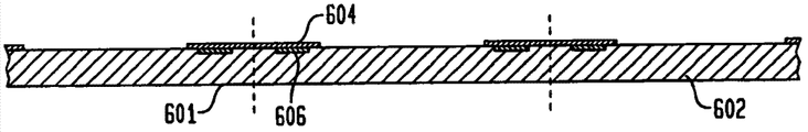
在一个实施例中,微电子装置的连接垫被置于芯片的结合垫处或其附近。对于某些构型来说,这就提供了足以形成与模板叠层内第二微电子装置的连接的金属表面可用区域。图6A示出模板600的透视图,其具有暴露于前面即接触-承载表面601处的结合垫606。该图类似于图1C。模板是带有一个或多个模板的晶片的一部分,该晶片可等同于图1A的晶片。金属化层可包括形成于芯片的结合垫之上或与其接触的连接垫604。在多种情形下,芯片的结合垫的间隔已经很小了,从而防止结合垫上的金属化层的宽度实际上比结合垫自身还宽。在本实施例的变型中,在结合垫上不提供金属层,如图6B所示。在图6B中,结合垫靠近边缘且可延伸至模板区域的边缘,从而第二金属化步骤可借助导电元件将每个结合垫连接于芯片的另一表面。在其他方面,工艺接下来的步骤与就图6A的结构而论相类似。
In one embodiment, the connection pads of the microelectronic device are placed at or near the bond pads of the chip. For some configurations, this provides enough available area of the metal surface to form a connection to a second microelectronic device within the template stack. FIG. 6A shows a perspective view of a
再看图6A,基板602如晶片以与图2E概述的工艺类似的方式被加工。图6C示出示例性基板602的截面图,其包括带有覆盖其下面的结合垫606的金属化层604的多个模板600,尽管在结合垫上没有金属化层的情形下(图6B),可越过(by pass)第一金属化步骤。在图6D中,根据一个实施例,基板被翻转且通过粘合层608结合于临时基板610。图6E示出在模板的后表面变薄后的基板602。图6F示出基板602被切割或蚀刻以暴露出第一金属化层604(变型中或为结合垫)时的基板602。接着,根据一个实施 例,在变薄和蚀刻的基板上覆盖有绝缘钝化层614,第一金属化层的一部分仍然暴露在外,如图6G所示。根据一个实施例,沉积第二金属化层,形成连接第一和第二金属化层的连接垫616和导电元件618。得到的结构如图6H所示。在沿虚线切割后,微电子装置620的最终结构如图6I所示。
Referring again to Figure 6A, a
各微电子装置620可被接合以提供类似于前述实施例的模板叠层。图7示出示例性模板叠层组件700。模板叠层中的各个独立装置可通过如图4A和4B所示的方法被接合,所述方法将一个微电子装置前表面处的连接垫604与邻近该装置的微电子装置后表面处暴露的连接垫616的相接合。可选地,各微电子装置可被设置为其前表面彼此相对并且各前表面上的垫用该方法相接合。在另一变型中,各微电子装置可被设置成使各后表面彼此相对且其上的垫被接合。因为装置620的各连接垫处的接合面积典型地小于这样的一个装置200(图2),必须额外注意将每个装置与其它装置正确对齐。此处示出的模板叠层700使用相同的元件,但也可由不同尺寸和/或功能的各装置形成。
Each microelectronic device 620 can be bonded to provide a template stack similar to the previous embodiments. FIG. 7 illustrates an exemplary
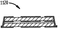
在另一实施例中,叠层中模板之间的连接可在接合步骤之后进行。图8A示出单个的微电子装置800。装置800的形成类似于图2和图7的装置。暴露于边缘804处的导电元件812不是用于为模板的另一表面提供环绕桥,而是连接元件(如粘合带、迹线或垫),以为下一个导电粘合提供表面区域。图8B示出了由装置800形成的模板叠层810的一个实施例。叠层中的每个装置都使用粘合层802连接于下一个装置。这样,各装置可能不是彼此电连接的。为导电地结合各装置,焊球或其他可流动材料806能在侧边缘附近沉积在叠层的顶部上。在施加热量时,可流动材料806向下流动以将暴露于叠层中各微电子装置边缘表面处的连接元件润湿并接合在一起。作为模板叠层组件810最终如图8B所示。
In another embodiment, the connection between the templates in the stack can be performed after the bonding step. FIG. 8A shows a single
在另一实施例中,上述制造方法(图1A-1I)能同时施加到两个或更多个基板上,将它们结合在一起形成具有整体堆叠的模板的微电子装置。一个示例性的工艺流程图如图9所示。在此实施例中,两个或更多个基板能在增加侧面导电元件之前在后表面处被接合。为此,基板被构图有第一金属化层并被连接到临时载体晶片。该基板通过研磨、抛光或其他一些方法被变薄。该工艺的结果如图10A所示,类似于图1F的结构117。在图10B 中,第二结构117被上下翻转且用粘合层1002连接于第一结构117。图10C示出去除了上临时载体晶片和上粘合层之后的中间晶片叠层1000。接下来,如图10D所示,穿过基板和中央粘合层1002切割或蚀刻通道1004以暴露下基板的第一金属化层。
In another embodiment, the fabrication method described above (FIGS. 1A-1I) can be applied simultaneously to two or more substrates, bonding them together to form a microelectronic device with an integrally stacked template. An exemplary process flow diagram is shown in FIG. 9 . In this embodiment, two or more substrates can be bonded at the rear surface before adding side conductive elements. For this, the substrate is patterned with a first metallization layer and connected to a temporary carrier wafer. The substrate is thinned by grinding, polishing or some other method. The result of this process is shown in Figure 10A, similar to structure 117 of Figure IF. In FIG. 10B , the
在本实施例中,因为基板的变薄表面朝中央粘合层面向内,独立的钝化步骤不是必需的。但是,因为在通道内可能有基板的未保护区域(这取决于通道是如何形成的),在形成通道后钝化步骤可被添加为可选步骤。图10E示出金属化层被沉积和构图从而在边缘表面处形成侧面导电元件1012后的晶片结构1010,该导电元件将每个装置1020的第一表面1001上的导体如迹线、连接垫连接于装置的第二表面1003上的导电元件。要注意,在第三金属化层形成将叠层的顶部连接于底部的侧面导电元件1012的同时,它也与上基板的被构图金属化层重叠以形成各金属化层之间的导电路径。虽然这些金属层有些重叠,但使用该方法整个工艺可被简化且实现成本节约,因为相同的结构可被用作工艺的一部分。在虚线处分离后,形成中间模板叠层装置1020且如图10F所示。类似于前述实施例,可使用如参照图4B、7或8A-C的上述方法将模板叠层装置1020接合于复合叠层1030中的其它类似装置。虽然装置1020被称为中间模板叠层装置,可以想到该装置可被封装和独自使用而不进行接下来的堆叠。
In this embodiment, a separate passivation step is not necessary because the thinned surface of the substrate faces inwards towards the central bonding layer. However, since there may be unprotected areas of the substrate within the channel (depending on how the channel is formed), a passivation step may be added as an optional step after forming the channel. 10E shows the
在一个变型中,可省略上基板上的第一金属化层。这样的一个示例是图10H所示的结构1040。在该变型中,用粘合层将结构1040接合于下基板,且随之形成通道1004。金属化层的沉积和接下来的构图将导致结构的外观和功能与图10E的结构1010基本相同,接着结构可以相同方式被加工和进一步堆叠。该变型中的两个晶片基板可被形成的略微不同,取消工艺中所需的金属化步骤之一。
In a variant, the first metallization layer on the upper substrate may be omitted. An example of this is
在本实施例的另一变型中,此时没有附图,第二晶片叠层1000可被翻转且用另一粘合层连接于第一晶片叠层1000,接着再次去除上载体晶片。接着可切割和金属化该组件以形成四级连接的被堆叠装置。
In another variation of this embodiment, not shown at this time, the
在又一实施例中,可在将两个基板电连接之前以表面朝下的方式加工它们。图11A示出将被连接的两个晶片结构,它们与图1C所示的结构111和图1F所示的结构117基本相同。不是将结构111连接于将被变薄的临时 载体晶片(如图1E所示),而是直接将其连接于结构117的背面。这如图11B所示,其中两个结构都连接有粘合层1102。图11C示出上基板变薄的结果。之后,如图11D所示穿过基板和中央金属化层形成通道。在图11E中,第三金属化层被沉积和构图以形成结构1110。此时注意,第三金属化层的边缘导电元件部分1112与其它金属化层都接触。最后,去除下载体并且装置1120如图11F所示被分离。这些装置可被堆叠为如图11G所示的模板叠层组件1130或其它样式。
In yet another embodiment, the two substrates may be processed face down before they are electrically connected. FIG. 11A shows two wafer structures to be joined, which are substantially the same as
虽然已经参照特定实施例描述了本发明,要了解这些实施例仅为对本发明原理和应用的示例。因此要理解,在不脱离所附权利要求限定的本发明的精神和范围的情况下可对示例性实施例做出多种改进并且可设计出其它结构。 While the invention has been described with reference to specific embodiments, it is to be understood that these embodiments are merely illustrative of the principles and applications of the invention. It is therefore to be understood that various modifications may be made to the exemplary embodiments and other structures may be devised without departing from the spirit and scope of the invention as defined by the appended claims. the
Claims (27)
Applications Claiming Priority (3)
| Application Number | Priority Date | Filing Date | Title |
|---|---|---|---|
| US6195308P | 2008-06-16 | 2008-06-16 | |
| US61/061,953 | 2008-06-16 | ||
| PCT/US2009/003643 WO2009154761A1 (en) | 2008-06-16 | 2009-06-15 | Stacking of wafer-level chip scale packages having edge contacts |
Publications (2)
| Publication Number | Publication Date |
|---|---|
| CN102067310A CN102067310A (en) | 2011-05-18 |
| CN102067310B true CN102067310B (en) | 2013-08-21 |
Family
ID=40974425
Family Applications (1)
| Application Number | Title | Priority Date | Filing Date |
|---|---|---|---|
| CN2009801225230A Active CN102067310B (en) | 2008-06-16 | 2009-06-15 | Stacking of wafer-level chip scale packages having edge contacts and manufacture method thereof |
Country Status (7)
| Country | Link |
|---|---|
| US (1) | US8680662B2 (en) |
| EP (1) | EP2308087B1 (en) |
| JP (1) | JP5639052B2 (en) |
| KR (1) | KR101655897B1 (en) |
| CN (1) | CN102067310B (en) |
| TW (1) | TWI425611B (en) |
| WO (1) | WO2009154761A1 (en) |
Families Citing this family (70)
| Publication number | Priority date | Publication date | Assignee | Title |
|---|---|---|---|---|
| US7215018B2 (en) | 2004-04-13 | 2007-05-08 | Vertical Circuits, Inc. | Stacked die BGA or LGA component assembly |
| US7829438B2 (en) | 2006-10-10 | 2010-11-09 | Tessera, Inc. | Edge connect wafer level stacking |
| US7901989B2 (en) | 2006-10-10 | 2011-03-08 | Tessera, Inc. | Reconstituted wafer level stacking |
| US8513789B2 (en) | 2006-10-10 | 2013-08-20 | Tessera, Inc. | Edge connect wafer level stacking with leads extending along edges |
| US7952195B2 (en) | 2006-12-28 | 2011-05-31 | Tessera, Inc. | Stacked packages with bridging traces |
| US8723332B2 (en) | 2007-06-11 | 2014-05-13 | Invensas Corporation | Electrically interconnected stacked die assemblies |
| KR101458538B1 (en) | 2007-07-27 | 2014-11-07 | 테세라, 인코포레이티드 | A stacked microelectronic unit, and method of fabrication thereof |
| US8551815B2 (en) | 2007-08-03 | 2013-10-08 | Tessera, Inc. | Stack packages using reconstituted wafers |
| US8043895B2 (en) | 2007-08-09 | 2011-10-25 | Tessera, Inc. | Method of fabricating stacked assembly including plurality of stacked microelectronic elements |
| US8704379B2 (en) | 2007-09-10 | 2014-04-22 | Invensas Corporation | Semiconductor die mount by conformal die coating |
| US8178978B2 (en) | 2008-03-12 | 2012-05-15 | Vertical Circuits, Inc. | Support mounted electrically interconnected die assembly |
| US9153517B2 (en) | 2008-05-20 | 2015-10-06 | Invensas Corporation | Electrical connector between die pad and z-interconnect for stacked die assemblies |
| US7863159B2 (en) | 2008-06-19 | 2011-01-04 | Vertical Circuits, Inc. | Semiconductor die separation method |
| CN102067310B (en) | 2008-06-16 | 2013-08-21 | 泰塞拉公司 | Stacking of wafer-level chip scale packages having edge contacts and manufacture method thereof |
| CN102422412A (en) | 2009-03-13 | 2012-04-18 | 德塞拉股份有限公司 | Stacked microelectronic assemblies having vias extending through bond pads |
| JP5963671B2 (en) | 2009-06-26 | 2016-08-03 | インヴェンサス・コーポレーション | Electrical interconnection for stacked dies in zigzag configuration |
| US8242543B2 (en) * | 2009-08-26 | 2012-08-14 | Qualcomm Incorporated | Semiconductor wafer-to-wafer bonding for dissimilar semiconductor dies and/or wafers |
| WO2011056668A2 (en) | 2009-10-27 | 2011-05-12 | Vertical Circuits, Inc. | Selective die electrical insulation additive process |
| TWI544604B (en) | 2009-11-04 | 2016-08-01 | 英維瑟斯公司 | Stacked die assembly with reduced stress electrical interconnection |
| US20110221053A1 (en) * | 2010-03-11 | 2011-09-15 | Qualcomm Incorporated | Pre-processing to reduce wafer level warpage |
| US8796137B2 (en) * | 2010-06-24 | 2014-08-05 | Stats Chippac, Ltd. | Semiconductor device and method of forming RDL along sloped side surface of semiconductor die for z-direction interconnect |
| US8482111B2 (en) | 2010-07-19 | 2013-07-09 | Tessera, Inc. | Stackable molded microelectronic packages |
| US11830845B2 (en) | 2011-05-03 | 2023-11-28 | Tessera Llc | Package-on-package assembly with wire bonds to encapsulation surface |
| KR101128063B1 (en) | 2011-05-03 | 2012-04-23 | 테세라, 인코포레이티드 | Package-on-package assembly with wire bonds to encapsulation surface |
| US8404520B1 (en) | 2011-10-17 | 2013-03-26 | Invensas Corporation | Package-on-package assembly with wire bond vias |
| US8946757B2 (en) | 2012-02-17 | 2015-02-03 | Invensas Corporation | Heat spreading substrate with embedded interconnects |
| US8372741B1 (en) | 2012-02-24 | 2013-02-12 | Invensas Corporation | Method for package-on-package assembly with wire bonds to encapsulation surface |
| US8835228B2 (en) | 2012-05-22 | 2014-09-16 | Invensas Corporation | Substrate-less stackable package with wire-bond interconnect |
| CN103515257A (en) * | 2012-06-18 | 2014-01-15 | 智瑞达科技(苏州)有限公司 | High-density semiconductor packaging structure packaging method |
| US9391008B2 (en) * | 2012-07-31 | 2016-07-12 | Invensas Corporation | Reconstituted wafer-level package DRAM |
| US9502390B2 (en) | 2012-08-03 | 2016-11-22 | Invensas Corporation | BVA interposer |
| US20140306331A1 (en) * | 2013-04-11 | 2014-10-16 | Infineon Technologies Austria Ag | Chip and chip arrangement |
| US20140326856A1 (en) * | 2013-05-06 | 2014-11-06 | Omnivision Technologies, Inc. | Integrated circuit stack with low profile contacts |
| US9167710B2 (en) | 2013-08-07 | 2015-10-20 | Invensas Corporation | Embedded packaging with preformed vias |
| US9685365B2 (en) | 2013-08-08 | 2017-06-20 | Invensas Corporation | Method of forming a wire bond having a free end |
| US20150076714A1 (en) | 2013-09-16 | 2015-03-19 | Invensas Corporation | Microelectronic element with bond elements to encapsulation surface |
| US9263394B2 (en) | 2013-11-22 | 2016-02-16 | Invensas Corporation | Multiple bond via arrays of different wire heights on a same substrate |
| US9583456B2 (en) | 2013-11-22 | 2017-02-28 | Invensas Corporation | Multiple bond via arrays of different wire heights on a same substrate |
| US9379074B2 (en) | 2013-11-22 | 2016-06-28 | Invensas Corporation | Die stacks with one or more bond via arrays of wire bond wires and with one or more arrays of bump interconnects |
| US9583411B2 (en) | 2014-01-17 | 2017-02-28 | Invensas Corporation | Fine pitch BVA using reconstituted wafer with area array accessible for testing |
| US10381326B2 (en) | 2014-05-28 | 2019-08-13 | Invensas Corporation | Structure and method for integrated circuits packaging with increased density |
| US9735084B2 (en) | 2014-12-11 | 2017-08-15 | Invensas Corporation | Bond via array for thermal conductivity |
| US9888579B2 (en) | 2015-03-05 | 2018-02-06 | Invensas Corporation | Pressing of wire bond wire tips to provide bent-over tips |
| US9502372B1 (en) | 2015-04-30 | 2016-11-22 | Invensas Corporation | Wafer-level packaging using wire bond wires in place of a redistribution layer |
| US9761554B2 (en) | 2015-05-07 | 2017-09-12 | Invensas Corporation | Ball bonding metal wire bond wires to metal pads |
| US9871019B2 (en) | 2015-07-17 | 2018-01-16 | Invensas Corporation | Flipped die stack assemblies with leadframe interconnects |
| US9490195B1 (en) | 2015-07-17 | 2016-11-08 | Invensas Corporation | Wafer-level flipped die stacks with leadframes or metal foil interconnects |
| US9825002B2 (en) | 2015-07-17 | 2017-11-21 | Invensas Corporation | Flipped die stack |
| US10490528B2 (en) | 2015-10-12 | 2019-11-26 | Invensas Corporation | Embedded wire bond wires |
| US9490222B1 (en) | 2015-10-12 | 2016-11-08 | Invensas Corporation | Wire bond wires for interference shielding |
| US10332854B2 (en) | 2015-10-23 | 2019-06-25 | Invensas Corporation | Anchoring structure of fine pitch bva |
| US10181457B2 (en) | 2015-10-26 | 2019-01-15 | Invensas Corporation | Microelectronic package for wafer-level chip scale packaging with fan-out |
| US9911718B2 (en) | 2015-11-17 | 2018-03-06 | Invensas Corporation | ‘RDL-First’ packaged microelectronic device for a package-on-package device |
| US9659848B1 (en) | 2015-11-18 | 2017-05-23 | Invensas Corporation | Stiffened wires for offset BVA |
| US11037904B2 (en) * | 2015-11-24 | 2021-06-15 | Taiwan Semiconductor Manufacturing Company, Ltd. | Singulation and bonding methods and structures formed thereby |
| US9508691B1 (en) | 2015-12-16 | 2016-11-29 | Invensas Corporation | Flipped die stacks with multiple rows of leadframe interconnects |
| US9984992B2 (en) | 2015-12-30 | 2018-05-29 | Invensas Corporation | Embedded wire bond wires for vertical integration with separate surface mount and wire bond mounting surfaces |
| US10566310B2 (en) | 2016-04-11 | 2020-02-18 | Invensas Corporation | Microelectronic packages having stacked die and wire bond interconnects |
| US9595511B1 (en) | 2016-05-12 | 2017-03-14 | Invensas Corporation | Microelectronic packages and assemblies with improved flyby signaling operation |
| US9728524B1 (en) | 2016-06-30 | 2017-08-08 | Invensas Corporation | Enhanced density assembly having microelectronic packages mounted at substantial angle to board |
| US9935075B2 (en) | 2016-07-29 | 2018-04-03 | Invensas Corporation | Wire bonding method and apparatus for electromagnetic interference shielding |
| US9996725B2 (en) * | 2016-11-03 | 2018-06-12 | Optiz, Inc. | Under screen sensor assembly |
| CN110036565A (en) * | 2016-12-08 | 2019-07-19 | 株式会社村田制作所 | Composite component and its mounting structure |
| US10299368B2 (en) | 2016-12-21 | 2019-05-21 | Invensas Corporation | Surface integrated waveguides and circuit structures therefor |
| DE102017109670B4 (en) * | 2017-05-05 | 2019-12-24 | Infineon Technologies Ag | Manufacturing process for a chip package with side wall metallization |
| US12506055B2 (en) | 2017-11-29 | 2025-12-23 | Pep Innovation Pte. Ltd. | Chip packaging method and chip structure |
| KR102435517B1 (en) * | 2018-04-12 | 2022-08-22 | 에스케이하이닉스 주식회사 | Chip stack package |
| CN110648930A (en) * | 2019-03-26 | 2020-01-03 | Pep创新私人有限公司 | Packaging method, panel assembly, wafer package and chip package |
| US11393791B2 (en) * | 2020-01-28 | 2022-07-19 | Micron Technology, Inc. | Three-dimensional stacking semiconductor assemblies with near zero bond line thickness |
| JP2022049485A (en) | 2020-09-16 | 2022-03-29 | キオクシア株式会社 | Semiconductor storage device |
Citations (2)
| Publication number | Priority date | Publication date | Assignee | Title |
|---|---|---|---|---|
| JP2002093944A (en) * | 2000-09-11 | 2002-03-29 | Oki Electric Ind Co Ltd | Semiconductor device, method of manufacturing semiconductor device, stack type semiconductor device, and method of manufacturing stack type semiconductor device |
| TW200405581A (en) * | 2002-05-13 | 2004-04-01 | Nat Semiconductor Corp | Electrical die contact structure and fabrication method |
Family Cites Families (251)
| Publication number | Priority date | Publication date | Assignee | Title |
|---|---|---|---|---|
| US4074342A (en) | 1974-12-20 | 1978-02-14 | International Business Machines Corporation | Electrical package for lsi devices and assembly process therefor |
| US4500905A (en) | 1981-09-30 | 1985-02-19 | Tokyo Shibaura Denki Kabushiki Kaisha | Stacked semiconductor device with sloping sides |
| US4897708A (en) | 1986-07-17 | 1990-01-30 | Laser Dynamics, Inc. | Semiconductor wafer array |
| US4954875A (en) | 1986-07-17 | 1990-09-04 | Laser Dynamics, Inc. | Semiconductor wafer array with electrically conductive compliant material |
| US4765864A (en) | 1987-07-15 | 1988-08-23 | Sri International | Etching method for producing an electrochemical cell in a crystalline substrate |
| US4842699A (en) | 1988-05-10 | 1989-06-27 | Avantek, Inc. | Method of selective via-hole and heat sink plating using a metal mask |
| JP2876773B2 (en) * | 1990-10-22 | 1999-03-31 | セイコーエプソン株式会社 | Program instruction word length variable type computing device and data processing device |
| US5614766A (en) | 1991-09-30 | 1997-03-25 | Rohm Co., Ltd. | Semiconductor device with stacked alternate-facing chips |
| WO1993023982A1 (en) | 1992-05-11 | 1993-11-25 | Nchip, Inc. | Stacked devices for multichip modules |
| US5322816A (en) | 1993-01-19 | 1994-06-21 | Hughes Aircraft Company | Method for forming deep conductive feedthroughs |
| US5426072A (en) | 1993-01-21 | 1995-06-20 | Hughes Aircraft Company | Process of manufacturing a three dimensional integrated circuit from stacked SOI wafers using a temporary silicon substrate |
| FR2704690B1 (en) | 1993-04-27 | 1995-06-23 | Thomson Csf | Method for encapsulating semiconductor wafers, device obtained by this process and application to the interconnection of wafers in three dimensions. |
| US5343071A (en) | 1993-04-28 | 1994-08-30 | Raytheon Company | Semiconductor structures having dual surface via holes |
| DE4314907C1 (en) | 1993-05-05 | 1994-08-25 | Siemens Ag | Method for producing semiconductor components making electrically conducting contact with one another vertically |
| IL106892A0 (en) | 1993-09-02 | 1993-12-28 | Pierre Badehi | Methods and apparatus for producing integrated circuit devices |
| US5412539A (en) | 1993-10-18 | 1995-05-02 | Hughes Aircraft Company | Multichip module with a mandrel-produced interconnecting decal |
| US5424245A (en) | 1994-01-04 | 1995-06-13 | Motorola, Inc. | Method of forming vias through two-sided substrate |
| IL108359A (en) | 1994-01-17 | 2001-04-30 | Shellcase Ltd | Method and apparatus for producing integrated circuit devices |
| US5502333A (en) | 1994-03-30 | 1996-03-26 | International Business Machines Corporation | Semiconductor stack structures and fabrication/sparing methods utilizing programmable spare circuit |
| US5675180A (en) | 1994-06-23 | 1997-10-07 | Cubic Memory, Inc. | Vertical interconnect process for silicon segments |
| US6228686B1 (en) * | 1995-09-18 | 2001-05-08 | Tessera, Inc. | Method of fabricating a microelectronic assembly using sheets with gaps to define lead regions |
| IL110261A0 (en) | 1994-07-10 | 1994-10-21 | Schellcase Ltd | Packaged integrated circuit |
| US5880010A (en) | 1994-07-12 | 1999-03-09 | Sun Microsystems, Inc. | Ultrathin electronics |
| MY114888A (en) | 1994-08-22 | 2003-02-28 | Ibm | Method for forming a monolithic electronic module by stacking planar arrays of integrated circuit chips |
| DE4433846C2 (en) | 1994-09-22 | 1999-06-02 | Fraunhofer Ges Forschung | Method of making a vertical integrated circuit structure |
| DE4433845A1 (en) | 1994-09-22 | 1996-03-28 | Fraunhofer Ges Forschung | Method of manufacturing a three-dimensional integrated circuit |
| US5466634A (en) | 1994-12-20 | 1995-11-14 | International Business Machines Corporation | Electronic modules with interconnected surface metallization layers and fabrication methods therefore |
| DE19516487C1 (en) | 1995-05-05 | 1996-07-25 | Fraunhofer Ges Forschung | Vertical integration process for microelectronic system |
| US5682062A (en) | 1995-06-05 | 1997-10-28 | Harris Corporation | System for interconnecting stacked integrated circuits |
| US5814889A (en) | 1995-06-05 | 1998-09-29 | Harris Corporation | Intergrated circuit with coaxial isolation and method |
| US5608264A (en) | 1995-06-05 | 1997-03-04 | Harris Corporation | Surface mountable integrated circuit with conductive vias |
| US5646067A (en) | 1995-06-05 | 1997-07-08 | Harris Corporation | Method of bonding wafers having vias including conductive material |
| US5618752A (en) | 1995-06-05 | 1997-04-08 | Harris Corporation | Method of fabrication of surface mountable integrated circuits |
| US5604673A (en) | 1995-06-07 | 1997-02-18 | Hughes Electronics | Low temperature co-fired ceramic substrates for power converters |
| US5648684A (en) | 1995-07-26 | 1997-07-15 | International Business Machines Corporation | Endcap chip with conductive, monolithic L-connect for multichip stack |
| US6002167A (en) | 1995-09-22 | 1999-12-14 | Hitachi Cable, Ltd. | Semiconductor device having lead on chip structure |
| JP2743904B2 (en) | 1996-02-16 | 1998-04-28 | 日本電気株式会社 | Semiconductor substrate and method of manufacturing semiconductor device using the same |
| US5817530A (en) | 1996-05-20 | 1998-10-06 | Micron Technology, Inc. | Use of conductive lines on the back side of wafers and dice for semiconductor interconnects |
| US6784023B2 (en) | 1996-05-20 | 2004-08-31 | Micron Technology, Inc. | Method of fabrication of stacked semiconductor devices |
| JP3620936B2 (en) | 1996-10-11 | 2005-02-16 | 浜松ホトニクス株式会社 | Back-illuminated light receiving device and manufacturing method thereof |
| KR100214562B1 (en) | 1997-03-24 | 1999-08-02 | 구본준 | Stacked semiconductor chip package and making method thereof |
| US6551857B2 (en) | 1997-04-04 | 2003-04-22 | Elm Technology Corporation | Three dimensional structure integrated circuits |
| US5915167A (en) | 1997-04-04 | 1999-06-22 | Elm Technology Corporation | Three dimensional structure memory |
| EP0926723B1 (en) | 1997-11-26 | 2007-01-17 | STMicroelectronics S.r.l. | Process for forming front-back through contacts in micro-integrated electronic devices |
| US6620731B1 (en) | 1997-12-18 | 2003-09-16 | Micron Technology, Inc. | Method for fabricating semiconductor components and interconnects with contacts on opposing sides |
| IL123207A0 (en) * | 1998-02-06 | 1998-09-24 | Shellcase Ltd | Integrated circuit device |
| US6624505B2 (en) | 1998-02-06 | 2003-09-23 | Shellcase, Ltd. | Packaged integrated circuits and methods of producing thereof |
| EP0985228A1 (en) | 1998-03-02 | 2000-03-15 | Koninklijke Philips Electronics N.V. | Semiconductor device comprising a glass supporting body onto which a substrate with semiconductor elements and a metallization is attached by means of an adhesive |
| US6982475B1 (en) | 1998-03-20 | 2006-01-03 | Mcsp, Llc | Hermetic wafer scale integrated circuit structure |
| KR100266693B1 (en) | 1998-05-30 | 2000-09-15 | 김영환 | Stackable ball grid array semiconductor package and fabrication method thereof |
| US6492201B1 (en) | 1998-07-10 | 2002-12-10 | Tessera, Inc. | Forming microelectronic connection components by electrophoretic deposition |
| US6103552A (en) | 1998-08-10 | 2000-08-15 | Lin; Mou-Shiung | Wafer scale packaging scheme |
| US6153929A (en) | 1998-08-21 | 2000-11-28 | Micron Technology, Inc. | Low profile multi-IC package connector |
| US6261865B1 (en) | 1998-10-06 | 2001-07-17 | Micron Technology, Inc. | Multi chip semiconductor package and method of construction |
| KR100304959B1 (en) | 1998-10-21 | 2001-09-24 | 김영환 | Chip stacked semiconductor package and manufacturing method thereof |
| SG78324A1 (en) | 1998-12-17 | 2001-02-20 | Eriston Technologies Pte Ltd | Bumpless flip chip assembly with strips-in-via and plating |
| US6229216B1 (en) | 1999-01-11 | 2001-05-08 | Intel Corporation | Silicon interposer and multi-chip-module (MCM) with through substrate vias |
| JP3228257B2 (en) | 1999-01-22 | 2001-11-12 | 日本電気株式会社 | Memory package |
| US6130823A (en) | 1999-02-01 | 2000-10-10 | Raytheon E-Systems, Inc. | Stackable ball grid array module and method |
| US6204562B1 (en) | 1999-02-11 | 2001-03-20 | United Microelectronics Corp. | Wafer-level chip scale package |
| EP1041624A1 (en) | 1999-04-02 | 2000-10-04 | Interuniversitair Microelektronica Centrum Vzw | Method of transferring ultra-thin substrates and application of the method to the manufacture of a multilayer thin film device |
| JP3532788B2 (en) | 1999-04-13 | 2004-05-31 | 唯知 須賀 | Semiconductor device and manufacturing method thereof |
| US20030233704A1 (en) | 2000-04-17 | 2003-12-25 | Miguel Castellote | Air massage system for bathtub |
| WO2000074134A1 (en) | 1999-05-27 | 2000-12-07 | Fraunhofer-Gesellschaft zur Förderung der angewandten Forschung e.V. | Method for the vertical integration of electric components by |
| JP2001035995A (en) | 1999-07-22 | 2001-02-09 | Seiko Epson Corp | Method for forming through hole in semiconductor chip |
| WO2001015228A1 (en) | 1999-08-19 | 2001-03-01 | Seiko Epson Corporation | Wiring board, method of manufacturing wiring board, electronic device, method of manufacturing electronic device, circuit board and electronic apparatus |
| US6277669B1 (en) | 1999-09-15 | 2001-08-21 | Industrial Technology Research Institute | Wafer level packaging method and packages formed |
| JP2001156250A (en) * | 1999-11-24 | 2001-06-08 | Seiko Epson Corp | Semiconductor chip, multi-chip package, semiconductor device, and electronic equipment using the same |
| IL133453A0 (en) | 1999-12-10 | 2001-04-30 | Shellcase Ltd | Methods for producing packaged integrated circuit devices and packaged integrated circuit devices produced thereby |
| US6621155B1 (en) | 1999-12-23 | 2003-09-16 | Rambus Inc. | Integrated circuit device having stacked dies and impedance balanced transmission lines |
| US6376904B1 (en) | 1999-12-23 | 2002-04-23 | Rambus Inc. | Redistributed bond pads in stacked integrated circuit die package |
| JP3879351B2 (en) | 2000-01-27 | 2007-02-14 | セイコーエプソン株式会社 | Manufacturing method of semiconductor chip |
| JP3684978B2 (en) | 2000-02-03 | 2005-08-17 | セイコーエプソン株式会社 | SEMICONDUCTOR DEVICE, ITS MANUFACTURING METHOD, AND ELECTRONIC DEVICE |
| JP2001223323A (en) | 2000-02-10 | 2001-08-17 | Mitsubishi Electric Corp | Semiconductor device |
| US6498387B1 (en) | 2000-02-15 | 2002-12-24 | Wen-Ken Yang | Wafer level package and the process of the same |
| US6252305B1 (en) | 2000-02-29 | 2001-06-26 | Advanced Semiconductor Engineering, Inc. | Multichip module having a stacked chip arrangement |
| US6344401B1 (en) | 2000-03-09 | 2002-02-05 | Atmel Corporation | Method of forming a stacked-die integrated circuit chip package on a water level |
| US6396710B1 (en) | 2000-05-12 | 2002-05-28 | Raytheon Company | High density interconnect module |
| JP3879816B2 (en) | 2000-06-02 | 2007-02-14 | セイコーエプソン株式会社 | SEMICONDUCTOR DEVICE AND ITS MANUFACTURING METHOD, LAMINATED SEMICONDUCTOR DEVICE, CIRCUIT BOARD AND ELECTRONIC DEVICE |
| US6472247B1 (en) | 2000-06-26 | 2002-10-29 | Ricoh Company, Ltd. | Solid-state imaging device and method of production of the same |
| JP3433193B2 (en) | 2000-10-23 | 2003-08-04 | 松下電器産業株式会社 | Semiconductor chip and manufacturing method thereof |
| US6693358B2 (en) | 2000-10-23 | 2004-02-17 | Matsushita Electric Industrial Co., Ltd. | Semiconductor chip, wiring board and manufacturing process thereof as well as semiconductor device |
| JP4505983B2 (en) | 2000-12-01 | 2010-07-21 | 日本電気株式会社 | Semiconductor device |
| JP3420748B2 (en) | 2000-12-14 | 2003-06-30 | 松下電器産業株式会社 | Semiconductor device and manufacturing method thereof |
| JP2002184937A (en) | 2000-12-18 | 2002-06-28 | Shinko Electric Ind Co Ltd | Semiconductor device mounting structure |
| US20020074637A1 (en) | 2000-12-19 | 2002-06-20 | Intel Corporation | Stacked flip chip assemblies |
| KR100855015B1 (en) | 2000-12-21 | 2008-08-28 | 테쎄라 테크놀로지스 헝가리 케이에프티. | Packaged integrated circuit and manufacturing method thereof |
| JP3915513B2 (en) | 2001-01-12 | 2007-05-16 | コニカミノルタホールディングス株式会社 | Imaging device |
| US20020098620A1 (en) | 2001-01-24 | 2002-07-25 | Yi-Chuan Ding | Chip scale package and manufacturing method thereof |
| KR100352236B1 (en) | 2001-01-30 | 2002-09-12 | 삼성전자 주식회사 | Wafer level package including ground metal layer |
| WO2002063681A1 (en) | 2001-02-08 | 2002-08-15 | Hitachi, Ltd. | Semiconductor integrated circuit device and its manufacturing method |
| KR100364635B1 (en) | 2001-02-09 | 2002-12-16 | 삼성전자 주식회사 | Chip-Level Three-Dimensional Multi-Chip Package Having Chip Selection Pad Formed On Chip-Level And Making Method Therefor |
| US6498381B2 (en) | 2001-02-22 | 2002-12-24 | Tru-Si Technologies, Inc. | Semiconductor structures having multiple conductive layers in an opening, and methods for fabricating same |
| US6717254B2 (en) | 2001-02-22 | 2004-04-06 | Tru-Si Technologies, Inc. | Devices having substrates with opening passing through the substrates and conductors in the openings, and methods of manufacture |
| US7115986B2 (en) * | 2001-05-02 | 2006-10-03 | Micron Technology, Inc. | Flexible ball grid array chip scale packages |
| US6528408B2 (en) | 2001-05-21 | 2003-03-04 | Micron Technology, Inc. | Method for bumped die and wire bonded board-on-chip package |
| JP3651413B2 (en) | 2001-05-21 | 2005-05-25 | 日立電線株式会社 | Semiconductor device tape carrier, semiconductor device using the same, semiconductor device tape carrier manufacturing method, and semiconductor device manufacturing method |
| US6878608B2 (en) | 2001-05-31 | 2005-04-12 | International Business Machines Corporation | Method of manufacture of silicon based package |
| US20030006494A1 (en) | 2001-07-03 | 2003-01-09 | Lee Sang Ho | Thin profile stackable semiconductor package and method for manufacturing |
| JP3660918B2 (en) * | 2001-07-04 | 2005-06-15 | 松下電器産業株式会社 | Semiconductor device and manufacturing method thereof |
| KR100394808B1 (en) | 2001-07-19 | 2003-08-14 | 삼성전자주식회사 | Wafer level stack chip package and method for manufacturing the same |
| US6787916B2 (en) | 2001-09-13 | 2004-09-07 | Tru-Si Technologies, Inc. | Structures having a substrate with a cavity and having an integrated circuit bonded to a contact pad located in the cavity |
| US6727576B2 (en) | 2001-10-31 | 2004-04-27 | Infineon Technologies Ag | Transfer wafer level packaging |
| US6611052B2 (en) | 2001-11-16 | 2003-08-26 | Micron Technology, Inc. | Wafer level stackable semiconductor package |
| JP2003163324A (en) | 2001-11-27 | 2003-06-06 | Nec Corp | Unit semiconductor device, method of manufacturing the same, and three-dimensional stacked semiconductor device |
| US6607941B2 (en) | 2002-01-11 | 2003-08-19 | National Semiconductor Corporation | Process and structure improvements to shellcase style packaging technology |
| US6743660B2 (en) | 2002-01-12 | 2004-06-01 | Taiwan Semiconductor Manufacturing Co., Ltd | Method of making a wafer level chip scale package |
| JP4002106B2 (en) | 2002-01-16 | 2007-10-31 | 日立オムロンターミナルソリューションズ株式会社 | Automatic transaction equipment |
| KR100486832B1 (en) | 2002-02-06 | 2005-05-03 | 삼성전자주식회사 | Semiconductor Chip, Chip Stack Package And Manufacturing Method |
| US6806559B2 (en) | 2002-04-22 | 2004-10-19 | Irvine Sensors Corporation | Method and apparatus for connecting vertically stacked integrated circuit chips |
| TWI232560B (en) | 2002-04-23 | 2005-05-11 | Sanyo Electric Co | Semiconductor device and its manufacture |
| JP2003318178A (en) | 2002-04-24 | 2003-11-07 | Seiko Epson Corp | Semiconductor device and its manufacturing method, circuit board, and electronic equipment |
| TWI229435B (en) | 2002-06-18 | 2005-03-11 | Sanyo Electric Co | Manufacture of semiconductor device |
| JP4215571B2 (en) * | 2002-06-18 | 2009-01-28 | 三洋電機株式会社 | Manufacturing method of semiconductor device |
| US6984545B2 (en) | 2002-07-22 | 2006-01-10 | Micron Technology, Inc. | Methods of encapsulating selected locations of a semiconductor die assembly using a thick solder mask |
| JP2004063569A (en) | 2002-07-25 | 2004-02-26 | Seiko Epson Corp | Semiconductor device and its manufacturing method, circuit board, and electronic equipment |
| US6903442B2 (en) | 2002-08-29 | 2005-06-07 | Micron Technology, Inc. | Semiconductor component having backside pin contacts |
| US7329563B2 (en) | 2002-09-03 | 2008-02-12 | Industrial Technology Research Institute | Method for fabrication of wafer level package incorporating dual compliant layers |
| SE0202681D0 (en) | 2002-09-10 | 2002-09-10 | Frank Niklaus | Hermetic sealing with combined adhesive bonding and sealing rings |
| US20040061213A1 (en) | 2002-09-17 | 2004-04-01 | Chippac, Inc. | Semiconductor multi-package module having package stacked over die-up flip chip ball grid array package and having wire bond interconnect between stacked packages |
| JP4081666B2 (en) | 2002-09-24 | 2008-04-30 | セイコーエプソン株式会社 | Semiconductor device and manufacturing method thereof, circuit board, and electronic apparatus |
| US20040104454A1 (en) | 2002-10-10 | 2004-06-03 | Rohm Co., Ltd. | Semiconductor device and method of producing the same |
| TWI227050B (en) | 2002-10-11 | 2005-01-21 | Sanyo Electric Co | Semiconductor device and method for manufacturing the same |
| US6656827B1 (en) | 2002-10-17 | 2003-12-02 | Taiwan Semiconductor Manufacturing Co., Ltd. | Electrical performance enhanced wafer level chip scale package with ground |
| US6869824B2 (en) | 2002-10-29 | 2005-03-22 | Ultratera Corporation | Fabrication method of window-type ball grid array semiconductor package |
| TWI227550B (en) | 2002-10-30 | 2005-02-01 | Sanyo Electric Co | Semiconductor device manufacturing method |
| JP2004153130A (en) | 2002-10-31 | 2004-05-27 | Olympus Corp | Semiconductor device and manufacturing method thereof |
| JP4056854B2 (en) | 2002-11-05 | 2008-03-05 | 新光電気工業株式会社 | Manufacturing method of semiconductor device |
| JP2004158536A (en) | 2002-11-05 | 2004-06-03 | Fujitsu Ltd | Semiconductor device and method of manufacturing semiconductor device |
| DE10253163B4 (en) | 2002-11-14 | 2015-07-23 | Epcos Ag | Hermetic encapsulation device and wafer scale manufacturing method |
| US20050012225A1 (en) | 2002-11-15 | 2005-01-20 | Choi Seung-Yong | Wafer-level chip scale package and method for fabricating and using the same |
| CN1650426A (en) | 2002-12-17 | 2005-08-03 | 富士通株式会社 | Semiconductor device and stacked semiconductor device |
| JP3566957B2 (en) | 2002-12-24 | 2004-09-15 | 沖電気工業株式会社 | Semiconductor device and manufacturing method thereof |
| KR20040059742A (en) | 2002-12-30 | 2004-07-06 | 동부전자 주식회사 | Packaging method of multi chip module for semiconductor |
| JP4145301B2 (en) | 2003-01-15 | 2008-09-03 | 富士通株式会社 | Semiconductor device and three-dimensional mounting semiconductor device |
| JP3680839B2 (en) | 2003-03-18 | 2005-08-10 | セイコーエプソン株式会社 | Semiconductor device and manufacturing method of semiconductor device |
| JP3972846B2 (en) | 2003-03-25 | 2007-09-05 | セイコーエプソン株式会社 | Manufacturing method of semiconductor device |
| EP1519410A1 (en) | 2003-09-25 | 2005-03-30 | Interuniversitair Microelektronica Centrum vzw ( IMEC) | Method for producing electrical through hole interconnects and devices made thereof |
| US6897148B2 (en) | 2003-04-09 | 2005-05-24 | Tru-Si Technologies, Inc. | Electroplating and electroless plating of conductive materials into openings, and structures obtained thereby |
| JP4373695B2 (en) | 2003-04-16 | 2009-11-25 | 浜松ホトニクス株式会社 | Manufacturing method of backside illuminated photodetector |
| SG119185A1 (en) | 2003-05-06 | 2006-02-28 | Micron Technology Inc | Method for packaging circuits and packaged circuits |
| JP2004342862A (en) | 2003-05-16 | 2004-12-02 | Sony Corp | Semiconductor device and its manufacturing method, pseudo wafer and its manufacturing method, and multi-chip module |
| EP1482553A3 (en) | 2003-05-26 | 2007-03-28 | Sanyo Electric Co., Ltd. | Semiconductor device and manufacturing method thereof |
| JP4130158B2 (en) | 2003-06-09 | 2008-08-06 | 三洋電機株式会社 | Semiconductor device manufacturing method, semiconductor device |
| CN100468719C (en) | 2003-06-03 | 2009-03-11 | 卡西欧计算机株式会社 | Stackable semiconductor device and manufacturing method thereof |
| US6972480B2 (en) | 2003-06-16 | 2005-12-06 | Shellcase Ltd. | Methods and apparatus for packaging integrated circuit devices |
| JP3646720B2 (en) | 2003-06-19 | 2005-05-11 | セイコーエプソン株式会社 | Semiconductor device and manufacturing method thereof, circuit board, and electronic apparatus |
| EP1639634B1 (en) | 2003-06-20 | 2009-04-01 | Nxp B.V. | Electronic device, assembly and methods of manufacturing an electronic device |
| WO2005004195A2 (en) | 2003-07-03 | 2005-01-13 | Shellcase Ltd. | Method and apparatus for packaging integrated circuit devices |
| JP2005045073A (en) | 2003-07-23 | 2005-02-17 | Hamamatsu Photonics Kk | Back-illuminated photodetection element |
| KR100537892B1 (en) | 2003-08-26 | 2005-12-21 | 삼성전자주식회사 | Chip stack package and manufacturing method thereof |
| US7180149B2 (en) | 2003-08-28 | 2007-02-20 | Fujikura Ltd. | Semiconductor package with through-hole |
| US7061085B2 (en) | 2003-09-19 | 2006-06-13 | Micron Technology, Inc. | Semiconductor component and system having stiffener and circuit decal |
| KR100594229B1 (en) | 2003-09-19 | 2006-07-03 | 삼성전자주식회사 | Semiconductor package and manufacturing method |
| JP2005101067A (en) | 2003-09-22 | 2005-04-14 | Sharp Corp | Substrate wiring structure and wiring forming method |
| US7298030B2 (en) | 2003-09-26 | 2007-11-20 | Tessera, Inc. | Structure and method of making sealed capped chips |
| SG120123A1 (en) * | 2003-09-30 | 2006-03-28 | Micron Technology Inc | Castellated chip-scale packages and methods for fabricating the same |
| KR100621992B1 (en) | 2003-11-19 | 2006-09-13 | 삼성전자주식회사 | Wafer Level Stack Structure and Method of Heterogeneous Devices and System-in-Package Using the Same |
| US7060601B2 (en) | 2003-12-17 | 2006-06-13 | Tru-Si Technologies, Inc. | Packaging substrates for integrated circuits and soldering methods |
| US7049170B2 (en) | 2003-12-17 | 2006-05-23 | Tru-Si Technologies, Inc. | Integrated circuits and packaging substrates with cavities, and attachment methods including insertion of protruding contact pads into cavities |
| US20050156330A1 (en) | 2004-01-21 | 2005-07-21 | Harris James M. | Through-wafer contact to bonding pad |
| DE102004008135A1 (en) | 2004-02-18 | 2005-09-22 | Infineon Technologies Ag | Semiconductor device with a stack of semiconductor chips and method for producing the same |
| US7160753B2 (en) | 2004-03-16 | 2007-01-09 | Voxtel, Inc. | Silicon-on-insulator active pixel sensors |
| JP4285309B2 (en) | 2004-04-13 | 2009-06-24 | パナソニック株式会社 | Electronic circuit module manufacturing method, multilayer electronic circuit module and manufacturing method thereof |
| US7215018B2 (en) | 2004-04-13 | 2007-05-08 | Vertical Circuits, Inc. | Stacked die BGA or LGA component assembly |
| US7952189B2 (en) | 2004-05-27 | 2011-05-31 | Chang-Feng Wan | Hermetic packaging and method of manufacture and use therefore |
| US7232754B2 (en) | 2004-06-29 | 2007-06-19 | Micron Technology, Inc. | Microelectronic devices and methods for forming interconnects in microelectronic devices |
| KR100587081B1 (en) | 2004-06-30 | 2006-06-08 | 주식회사 하이닉스반도체 | Semiconductor package with improved heat dissipation |
| JP4211696B2 (en) | 2004-06-30 | 2009-01-21 | ソニー株式会社 | Method for manufacturing solid-state imaging device |
| KR100605314B1 (en) | 2004-07-22 | 2006-07-28 | 삼성전자주식회사 | Method for Manufacturing Wafer Level Package with Rewiring Protective Film |
| DE102004039906A1 (en) | 2004-08-18 | 2005-08-18 | Infineon Technologies Ag | Electronic component with a number of integrated members, is formed by producing members with a surface that contains a circuit, and connecting components using bond wires |
| US20060043556A1 (en) | 2004-08-25 | 2006-03-02 | Chao-Yuan Su | Stacked packaging methods and structures |
| US7378342B2 (en) | 2004-08-27 | 2008-05-27 | Micron Technology, Inc. | Methods for forming vias varying lateral dimensions |
| US7129567B2 (en) | 2004-08-31 | 2006-10-31 | Micron Technology, Inc. | Substrate, semiconductor die, multichip module, and system including a via structure comprising a plurality of conductive elements |
| KR100604049B1 (en) | 2004-09-01 | 2006-07-24 | 동부일렉트로닉스 주식회사 | Semiconductor chip package and manufacturing method thereof |
| JP2006073825A (en) | 2004-09-02 | 2006-03-16 | Toshiba Corp | Semiconductor device and mounting method thereof |
| US7768795B2 (en) | 2004-09-08 | 2010-08-03 | Panasonic Corporation | Electronic circuit device, electronic device using the same, and method for manufacturing the same |
| TWI288448B (en) | 2004-09-10 | 2007-10-11 | Toshiba Corp | Semiconductor device and method of manufacturing the same |
| JP4139803B2 (en) | 2004-09-28 | 2008-08-27 | シャープ株式会社 | Manufacturing method of semiconductor device |
| KR100855819B1 (en) | 2004-10-08 | 2008-09-01 | 삼성전기주식회사 | MEMS package with metal sealing member |
| KR100676493B1 (en) | 2004-10-08 | 2007-02-01 | 디엔제이 클럽 인코 | Manufacturing Method of Wafer Level Chip Scale Package Using Redistribution Substrate |
| JP4873517B2 (en) | 2004-10-28 | 2012-02-08 | オンセミコンダクター・トレーディング・リミテッド | Semiconductor device and manufacturing method thereof |
| DE102004052921A1 (en) | 2004-10-29 | 2006-05-11 | Infineon Technologies Ag | Process for the production of semiconductor devices with external contacts |
| FR2879347A1 (en) | 2004-12-14 | 2006-06-16 | Commissariat Energie Atomique | ELECTRONIC DEVICE COMPRISING TWO COMPONENTS AND METHOD FOR MANUFACTURING SUCH A DEVICE |
| US20060138626A1 (en) | 2004-12-29 | 2006-06-29 | Tessera, Inc. | Microelectronic packages using a ceramic substrate having a window and a conductive surface region |
| KR20060087273A (en) | 2005-01-28 | 2006-08-02 | 삼성전기주식회사 | Semiconductor package and manufacturing method |
| US7675153B2 (en) | 2005-02-02 | 2010-03-09 | Kabushiki Kaisha Toshiba | Semiconductor device having semiconductor chips stacked and mounted thereon and manufacturing method thereof |
| US7538032B2 (en) | 2005-06-23 | 2009-05-26 | Teledyne Scientific & Imaging, Llc | Low temperature method for fabricating high-aspect ratio vias and devices fabricated by said method |
| US7449779B2 (en) | 2005-03-22 | 2008-11-11 | Tessera, Inc. | Wire bonded wafer level cavity package |
| US7326592B2 (en) | 2005-04-04 | 2008-02-05 | Infineon Technologies Ag | Stacked die package |
| JP4237160B2 (en) | 2005-04-08 | 2009-03-11 | エルピーダメモリ株式会社 | Multilayer semiconductor device |
| JP4308797B2 (en) | 2005-05-02 | 2009-08-05 | 株式会社アドバンストシステムズジャパン | Circuit board with semiconductor package and socket |
| US7208345B2 (en) | 2005-05-11 | 2007-04-24 | Infineon Technologies Ag | Method of manufacturing a semiconductor device comprising stacked chips and a corresponding semiconductor device |
| JP2007019107A (en) | 2005-07-05 | 2007-01-25 | Shinko Electric Ind Co Ltd | Semiconductor device and manufacturing method of semiconductor device |
| KR100629498B1 (en) | 2005-07-15 | 2006-09-28 | 삼성전자주식회사 | Micro-Packages, Multi-Stack Micro-Packages, and Methods for Making the Same |
| JP4551321B2 (en) | 2005-07-21 | 2010-09-29 | 新光電気工業株式会社 | Electronic component mounting structure and manufacturing method thereof |
| US7485968B2 (en) | 2005-08-11 | 2009-02-03 | Ziptronix, Inc. | 3D IC method and device |
| US7419853B2 (en) | 2005-08-11 | 2008-09-02 | Hymite A/S | Method of fabrication for chip scale package for a micro component |
| SG130066A1 (en) | 2005-08-26 | 2007-03-20 | Micron Technology Inc | Microelectronic device packages, stacked microelectronic device packages, and methods for manufacturing microelectronic devices |
| US7485969B2 (en) | 2005-09-01 | 2009-02-03 | Micron Technology, Inc. | Stacked microelectronic devices and methods for manufacturing microelectronic devices |
| US20070052050A1 (en) | 2005-09-07 | 2007-03-08 | Bart Dierickx | Backside thinned image sensor with integrated lens stack |
| KR20070048952A (en) | 2005-11-07 | 2007-05-10 | 삼성전자주식회사 | Multi-chip package with internal connection terminals |
| US20070126085A1 (en) | 2005-12-02 | 2007-06-07 | Nec Electronics Corporation | Semiconductor device and method of manufacturing the same |
| WO2007066409A1 (en) | 2005-12-09 | 2007-06-14 | Spansion Llc | Semiconductor device and its manufacturing method |
| US7981726B2 (en) | 2005-12-12 | 2011-07-19 | Intel Corporation | Copper plating connection for multi-die stack in substrate package |
| US7632708B2 (en) | 2005-12-27 | 2009-12-15 | Tessera, Inc. | Microelectronic component with photo-imageable substrate |
| US20070158807A1 (en) | 2005-12-29 | 2007-07-12 | Daoqiang Lu | Edge interconnects for die stacking |
| US20070190747A1 (en) | 2006-01-23 | 2007-08-16 | Tessera Technologies Hungary Kft. | Wafer level packaging to lidded chips |
| SG135074A1 (en) | 2006-02-28 | 2007-09-28 | Micron Technology Inc | Microelectronic devices, stacked microelectronic devices, and methods for manufacturing such devices |
| US7741707B2 (en) | 2006-02-27 | 2010-06-22 | Stats Chippac Ltd. | Stackable integrated circuit package system |
| US7510928B2 (en) | 2006-05-05 | 2009-03-31 | Tru-Si Technologies, Inc. | Dielectric trenches, nickel/tantalum oxide structures, and chemical mechanical polishing techniques |
| TWI367557B (en) | 2006-08-11 | 2012-07-01 | Sanyo Electric Co | Semiconductor device and manufaturing method thereof |
| US7888185B2 (en) | 2006-08-17 | 2011-02-15 | Micron Technology, Inc. | Semiconductor device assemblies and systems including at least one conductive pathway extending around a side of at least one semiconductor device |
| US7531445B2 (en) | 2006-09-26 | 2009-05-12 | Hymite A/S | Formation of through-wafer electrical interconnections and other structures using a thin dielectric membrane |
| US7829438B2 (en) | 2006-10-10 | 2010-11-09 | Tessera, Inc. | Edge connect wafer level stacking |
| US7901989B2 (en) | 2006-10-10 | 2011-03-08 | Tessera, Inc. | Reconstituted wafer level stacking |
| US8513789B2 (en) | 2006-10-10 | 2013-08-20 | Tessera, Inc. | Edge connect wafer level stacking with leads extending along edges |
| US7759166B2 (en) | 2006-10-17 | 2010-07-20 | Tessera, Inc. | Microelectronic packages fabricated at the wafer level and methods therefor |
| US7807508B2 (en) | 2006-10-31 | 2010-10-05 | Tessera Technologies Hungary Kft. | Wafer-level fabrication of lidded chips with electrodeposited dielectric coating |
| US7935568B2 (en) | 2006-10-31 | 2011-05-03 | Tessera Technologies Ireland Limited | Wafer-level fabrication of lidded chips with electrodeposited dielectric coating |
| US7394152B2 (en) | 2006-11-13 | 2008-07-01 | China Wafer Level Csp Ltd. | Wafer level chip size packaged chip device with an N-shape junction inside and method of fabricating the same |
| US7663213B2 (en) | 2006-11-13 | 2010-02-16 | China Wafer Level Csp Ltd. | Wafer level chip size packaged chip device with a double-layer lead structure and method of fabricating the same |
| US7791199B2 (en) | 2006-11-22 | 2010-09-07 | Tessera, Inc. | Packaged semiconductor chips |
| US8569876B2 (en) | 2006-11-22 | 2013-10-29 | Tessera, Inc. | Packaged semiconductor chips with array |
| US7952195B2 (en) | 2006-12-28 | 2011-05-31 | Tessera, Inc. | Stacked packages with bridging traces |
| US20080157327A1 (en) | 2007-01-03 | 2008-07-03 | Advanced Chip Engineering Technology Inc. | Package on package structure for semiconductor devices and method of the same |
| JP5584474B2 (en) | 2007-03-05 | 2014-09-03 | インヴェンサス・コーポレイション | Chip with rear contact connected to front contact by through via |
| US20080284041A1 (en) | 2007-05-18 | 2008-11-20 | Samsung Electronics Co., Ltd. | Semiconductor package with through silicon via and related method of fabrication |
| KR100914977B1 (en) | 2007-06-18 | 2009-09-02 | 주식회사 하이닉스반도체 | Method for fabricating stack package |
| WO2008157779A2 (en) * | 2007-06-20 | 2008-12-24 | Vertical Circuits, Inc. | Three-dimensional circuitry formed on integrated circuit device using two- dimensional fabrication |
| US20110024890A1 (en) | 2007-06-29 | 2011-02-03 | Stats Chippac, Ltd. | Stackable Package By Using Internal Stacking Modules |
| US8766910B2 (en) | 2007-07-04 | 2014-07-01 | Cypress Semiconductor Corporation | Capacitive sensing control knob |
| KR101458538B1 (en) | 2007-07-27 | 2014-11-07 | 테세라, 인코포레이티드 | A stacked microelectronic unit, and method of fabrication thereof |
| JP2009032929A (en) | 2007-07-27 | 2009-02-12 | Sanyo Electric Co Ltd | Semiconductor device and manufacturing method thereof |
| CN103178032B (en) | 2007-07-31 | 2017-06-20 | 英闻萨斯有限公司 | Use the method for packaging semiconductor for penetrating silicon passage |
| KR101387701B1 (en) | 2007-08-01 | 2014-04-23 | 삼성전자주식회사 | Semiconductor packages and methods for manufacturing the same |
| US8551815B2 (en) | 2007-08-03 | 2013-10-08 | Tessera, Inc. | Stack packages using reconstituted wafers |
| US8043895B2 (en) | 2007-08-09 | 2011-10-25 | Tessera, Inc. | Method of fabricating stacked assembly including plurality of stacked microelectronic elements |
| WO2009023462A1 (en) | 2007-08-10 | 2009-02-19 | Spansion Llc | Semiconductor device and method for manufacturing thereof |
| KR100905784B1 (en) | 2007-08-16 | 2009-07-02 | 주식회사 하이닉스반도체 | Through-electrode for semiconductor package and semiconductor package having same |
| KR20090047776A (en) | 2007-11-08 | 2009-05-13 | 삼성전자주식회사 | Semiconductor element and method of forming the same |
| KR101465948B1 (en) | 2007-12-27 | 2014-12-10 | 삼성전자주식회사 | A wafer level stack package and method of manufacturing a wafer level stack package |
| US8084854B2 (en) | 2007-12-28 | 2011-12-27 | Micron Technology, Inc. | Pass-through 3D interconnect for microelectronic dies and associated systems and methods |
| US20100053407A1 (en) | 2008-02-26 | 2010-03-04 | Tessera, Inc. | Wafer level compliant packages for rear-face illuminated solid state image sensors |
| US20090212381A1 (en) | 2008-02-26 | 2009-08-27 | Tessera, Inc. | Wafer level packages for rear-face illuminated solid state image sensors |
| US7973416B2 (en) | 2008-05-12 | 2011-07-05 | Texas Instruments Incorporated | Thru silicon enabled die stacking scheme |
| US7863721B2 (en) | 2008-06-11 | 2011-01-04 | Stats Chippac, Ltd. | Method and apparatus for wafer level integration using tapered vias |
| CN102067310B (en) | 2008-06-16 | 2013-08-21 | 泰塞拉公司 | Stacking of wafer-level chip scale packages having edge contacts and manufacture method thereof |
| US20100065949A1 (en) | 2008-09-17 | 2010-03-18 | Andreas Thies | Stacked Semiconductor Chips with Through Substrate Vias |
| KR100990943B1 (en) | 2008-11-07 | 2010-11-01 | 주식회사 하이닉스반도체 | Semiconductor package |
| CN102422412A (en) | 2009-03-13 | 2012-04-18 | 德塞拉股份有限公司 | Stacked microelectronic assemblies having vias extending through bond pads |
-
2009
- 2009-06-15 CN CN2009801225230A patent/CN102067310B/en active Active
- 2009-06-15 WO PCT/US2009/003643 patent/WO2009154761A1/en not_active Ceased
- 2009-06-15 KR KR1020107028161A patent/KR101655897B1/en not_active Expired - Fee Related
- 2009-06-15 US US12/456,349 patent/US8680662B2/en active Active
- 2009-06-15 JP JP2011514614A patent/JP5639052B2/en active Active
- 2009-06-15 EP EP09767074.9A patent/EP2308087B1/en not_active Not-in-force
- 2009-06-16 TW TW098120145A patent/TWI425611B/en not_active IP Right Cessation
Patent Citations (2)
| Publication number | Priority date | Publication date | Assignee | Title |
|---|---|---|---|---|
| JP2002093944A (en) * | 2000-09-11 | 2002-03-29 | Oki Electric Ind Co Ltd | Semiconductor device, method of manufacturing semiconductor device, stack type semiconductor device, and method of manufacturing stack type semiconductor device |
| TW200405581A (en) * | 2002-05-13 | 2004-04-01 | Nat Semiconductor Corp | Electrical die contact structure and fabrication method |
Also Published As
| Publication number | Publication date |
|---|---|
| JP5639052B2 (en) | 2014-12-10 |
| KR20110027690A (en) | 2011-03-16 |
| US20090316378A1 (en) | 2009-12-24 |
| TW201005918A (en) | 2010-02-01 |
| CN102067310A (en) | 2011-05-18 |
| US8680662B2 (en) | 2014-03-25 |
| EP2308087B1 (en) | 2020-08-12 |
| KR101655897B1 (en) | 2016-09-08 |
| TWI425611B (en) | 2014-02-01 |
| WO2009154761A1 (en) | 2009-12-23 |
| JP2011524647A (en) | 2011-09-01 |
| EP2308087A1 (en) | 2011-04-13 |
| WO2009154761A9 (en) | 2010-03-11 |
Similar Documents
| Publication | Publication Date | Title |
|---|---|---|
| CN102067310B (en) | Stacking of wafer-level chip scale packages having edge contacts and manufacture method thereof | |
| US12283566B2 (en) | Semiconductor device and method for manufacturing the same | |
| JP3186941B2 (en) | Semiconductor chips and multi-chip semiconductor modules | |
| US8786070B2 (en) | Microelectronic package with stacked microelectronic elements and method for manufacture thereof | |
| KR101245928B1 (en) | Ultra-thin stacked chips packaging | |
| US9508701B2 (en) | 3D device packaging using through-substrate pillars | |
| CN110098169A (en) | Electronic packing piece and its preparation method | |
| CN101154606A (en) | Manufacturing method of semiconductor device | |
| JP2013021058A (en) | Manufacturing method of semiconductor device | |
| US6972243B2 (en) | Fabrication of semiconductor dies with micro-pins and structures produced therewith | |
| TWI662677B (en) | Stacked package and a manufacturing method of the same | |
| CN101471269A (en) | Manufacturing method of semiconductor device | |
| WO2024021356A1 (en) | Tsv electrical connection structure having high aspect ratio and manufacturing method therefor | |
| CN101286459A (en) | Stackable semiconductor device and method for fabricating the same | |
| US20150179557A1 (en) | Semiconductor chips having heat conductive layer with vias | |
| CN109243981B (en) | Package structure and manufacturing method thereof | |
| JP2933037B2 (en) | Semiconductor device and manufacturing method thereof | |
| KR20130042938A (en) | Semiconductor chip, semiconductor package having the same, and method of fabricating stack type semiconductor package | |
| TWI514531B (en) | Semiconductor structure and its manufacturing method | |
| CN111863719A (en) | A chip interconnection method | |
| KR20140088756A (en) | High integrated multi layer interposer and method for manufacturing the same |
Legal Events
| Date | Code | Title | Description |
|---|---|---|---|
| C06 | Publication | ||
| PB01 | Publication | ||
| C10 | Entry into substantive examination | ||
| SE01 | Entry into force of request for substantive examination | ||
| ASS | Succession or assignment of patent right |
Owner name: TESSERA INC. Free format text: FORMER OWNER: TESSERA RESEARCH, LLC Effective date: 20111111 |
|
| C41 | Transfer of patent application or patent right or utility model | ||
| TA01 | Transfer of patent application right |
Effective date of registration: 20111111 Address after: American California Applicant after: Tessera Inc. Address before: American California Applicant before: Tessera Res LLC |
|
| C14 | Grant of patent or utility model | ||
| GR01 | Patent grant |