JP7526915B2 - Light emitting element - Google Patents
Light emitting element Download PDFInfo
- Publication number
- JP7526915B2 JP7526915B2 JP2021206191A JP2021206191A JP7526915B2 JP 7526915 B2 JP7526915 B2 JP 7526915B2 JP 2021206191 A JP2021206191 A JP 2021206191A JP 2021206191 A JP2021206191 A JP 2021206191A JP 7526915 B2 JP7526915 B2 JP 7526915B2
- Authority
- JP
- Japan
- Prior art keywords
- layer
- semiconductor layer
- side semiconductor
- type impurity
- impurity concentration
- Prior art date
- Legal status (The legal status is an assumption and is not a legal conclusion. Google has not performed a legal analysis and makes no representation as to the accuracy of the status listed.)
- Active
Links
Images


Classifications
-
- H—ELECTRICITY
- H10—SEMICONDUCTOR DEVICES; ELECTRIC SOLID-STATE DEVICES NOT OTHERWISE PROVIDED FOR
- H10H—INORGANIC LIGHT-EMITTING SEMICONDUCTOR DEVICES HAVING POTENTIAL BARRIERS
- H10H20/00—Individual inorganic light-emitting semiconductor devices having potential barriers, e.g. light-emitting diodes [LED]
- H10H20/80—Constructional details
- H10H20/81—Bodies
- H10H20/813—Bodies having a plurality of light-emitting regions, e.g. multi-junction LEDs or light-emitting devices having photoluminescent regions within the bodies
-
- H—ELECTRICITY
- H10—SEMICONDUCTOR DEVICES; ELECTRIC SOLID-STATE DEVICES NOT OTHERWISE PROVIDED FOR
- H10H—INORGANIC LIGHT-EMITTING SEMICONDUCTOR DEVICES HAVING POTENTIAL BARRIERS
- H10H20/00—Individual inorganic light-emitting semiconductor devices having potential barriers, e.g. light-emitting diodes [LED]
- H10H20/80—Constructional details
- H10H20/81—Bodies
- H10H20/822—Materials of the light-emitting regions
- H10H20/824—Materials of the light-emitting regions comprising only Group III-V materials, e.g. GaP
- H10H20/825—Materials of the light-emitting regions comprising only Group III-V materials, e.g. GaP containing nitrogen, e.g. GaN
- H10H20/8252—Materials of the light-emitting regions comprising only Group III-V materials, e.g. GaP containing nitrogen, e.g. GaN characterised by the dopants
-
- H—ELECTRICITY
- H10—SEMICONDUCTOR DEVICES; ELECTRIC SOLID-STATE DEVICES NOT OTHERWISE PROVIDED FOR
- H10H—INORGANIC LIGHT-EMITTING SEMICONDUCTOR DEVICES HAVING POTENTIAL BARRIERS
- H10H20/00—Individual inorganic light-emitting semiconductor devices having potential barriers, e.g. light-emitting diodes [LED]
- H10H20/80—Constructional details
- H10H20/81—Bodies
- H10H20/811—Bodies having quantum effect structures or superlattices, e.g. tunnel junctions
- H10H20/812—Bodies having quantum effect structures or superlattices, e.g. tunnel junctions within the light-emitting regions, e.g. having quantum confinement structures
Landscapes
- Led Devices (AREA)
Description
本発明は、発光素子に関する。 The present invention relates to a light-emitting element.
特許文献1には、例えば、第1のn型層、第1の活性層、および第1のp型層を含む第1発光部と、第1発光部上に配置されたトンネル接合層と、トンネル接合層上に配置され、第2のn型層、第2の活性層、および第2のp型層を含む第2発光部と、を備える発光素子が開示されている。 Patent Document 1 discloses, for example, a light-emitting element that includes a first light-emitting section including a first n-type layer, a first active layer, and a first p-type layer, a tunnel junction layer disposed on the first light-emitting section, and a second light-emitting section disposed on the tunnel junction layer and including a second n-type layer, a second active layer, and a second p-type layer.
本発明の一実施形態は、順方向電圧が低い発光素子を提供することを目的とする。 One embodiment of the present invention aims to provide a light-emitting element with a low forward voltage.
本発明の一実施形態に係る発光素子は、下方から上方に向かって順に、それぞれが窒化物半導体からなる、第1n側半導体層と、第1活性層と、第1p側半導体層と、前記第1p側半導体層に接する第2n側半導体層と、第2活性層と、第2p側半導体層と、を備える。前記第2n側半導体層は、下方から上方に向かって順に、第1層と、第2層と、第3層と、を有する。前記第1層は、インジウムおよびガリウムを含み、第1n型不純物濃度を有する。前記第2層は、インジウムおよびガリウムを含み、前記第1n型不純物濃度よりも低い第2n型不純物濃度を有する。前記第2層におけるインジウムの組成比の値は、前記第1層におけるインジウムの組成比の値よりも小さい。前記第2層の厚みは、前記第1層の厚みよりも大きい。前記第3層は、ガリウムを含み、前記第2n型不純物濃度よりも低い第3n型不純物濃度を有する。 A light-emitting element according to one embodiment of the present invention includes, in order from bottom to top, a first n-side semiconductor layer, a first active layer, a first p-side semiconductor layer, a second n-side semiconductor layer in contact with the first p-side semiconductor layer, a second active layer, and a second p-side semiconductor layer, each of which is made of a nitride semiconductor. The second n-side semiconductor layer includes, in order from bottom to top, a first layer, a second layer, and a third layer. The first layer includes indium and gallium and has a first n-type impurity concentration. The second layer includes indium and gallium and has a second n-type impurity concentration lower than the first n-type impurity concentration. The value of the indium composition ratio in the second layer is smaller than the value of the indium composition ratio in the first layer. The thickness of the second layer is larger than the thickness of the first layer. The third layer includes gallium and has a third n-type impurity concentration lower than the second n-type impurity concentration.
本発明の一実施形態によれば、順方向電圧が低い発光素子を提供できる。 According to one embodiment of the present invention, a light-emitting element with a low forward voltage can be provided.
以下に、実施形態について図面を参照しつつ説明する。なお、図面は模式的または概念的なものであり、各部分の厚みと幅との関係、部分間の大きさの比率などは、必ずしも現実のものと同一とは限らない。また、同じ部分を表す場合であっても、図面により互いの寸法や比率が異なって表される場合もある。さらに、本明細書と各図において、既出の図に関して説明したものと同様の要素には同一の符号を付して詳細な説明は適宜省略する。 The following describes the embodiments with reference to the drawings. Note that the drawings are schematic or conceptual, and the relationship between the thickness and width of each part, the size ratio between parts, etc. are not necessarily the same as in reality. Even when the same part is shown, the dimensions and ratios may be shown differently depending on the drawing. Furthermore, in this specification and each drawing, elements similar to those explained with reference to the previous drawings are given the same reference numerals, and detailed explanations are omitted as appropriate.
また、以下では、説明をわかりやすくするために、XYZ直交座標系を用いて、各部分の配置および構成を説明する。X軸、Y軸、Z軸は、相互に直交している。またX軸が延びる方向を「X方向」とし、Y軸が延びる方向を「Y方向」とし、Z軸が延びる方向を「Z方向」とする。また、説明をわかりやすくするために、上方をZ方向、下方をその反対方向とするが、これらの方向は、相対的なものであり重力方向とは無関係である。 In the following, for ease of understanding, the arrangement and configuration of each part will be explained using an XYZ Cartesian coordinate system. The X-axis, Y-axis, and Z-axis are mutually perpendicular. The direction in which the X-axis extends will be referred to as the "X-direction", the direction in which the Y-axis extends will be referred to as the "Y-direction", and the direction in which the Z-axis extends will be referred to as the "Z-direction". In order to ease of understanding, the upward direction will be referred to as the Z-direction and the downward direction will be referred to as the opposite direction, but these directions are relative and have no relation to the direction of gravity.
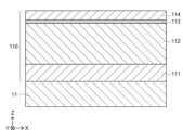
図1は、本実施形態に係る発光素子10を示す断面図である。
図2は、図1の第2n側半導体層121を拡大して示す断面図である。
図3は、本実施形態に係る発光素子10のエネルギーバンド図の例である。
発光素子10は、図1に示すように、基板11と、半導体構造体12と、n側電極13と、p側電極14と、を備える。
FIG. 1 is a cross-sectional view showing a light-
FIG. 2 is an enlarged cross-sectional view showing the second n-
FIG. 3 is an example of an energy band diagram of the
As shown in FIG. 1, the
基板11の形状は平板状である。基板11の上面および下面は、例えば、X-Y平面に概ね平行である。基板11は、例えば、サファイア(Al2O3)からなる。ただし、基板11には、シリコン(Si)、炭化シリコン(SiC)、または窒化ガリウム(GaN)等他の材料を用いてもよい。基板11の上には、半導体構造体12が配置されている。
The
半導体構造体12は、例えば、窒化物半導体からなる複数の半導体層が積層された積層体である。ここで、「窒化物半導体」とは、窒素を含む半導体であって、典型的には、InxAlyGa1-x-yN(0≦x≦1,0≦y≦1,x+y≦1)なる化学式において組成比xおよびyをそれぞれの範囲内で変化させた全ての組成の半導体を含むものである。
The
半導体構造体12は、下方から上方に向かって順に、第1発光部110と、第2発光部120と、を有する。第1発光部110は、下方から上方に向かって順に、第1n側半導体層112と、第1活性層113と、第1p側半導体層114と、を含む。第1発光部110は、第1n側半導体層112の下に配置された下地層111をさらに含む。第2発光部120は、下方から上方に向かって順に、第2n側半導体層121と、第2活性層122と、第2p側半導体層123と、を含む。以下、半導体構造体12の各部について詳述する。
The
第1発光部110の下地層111は、基板11の上に配置されている。下地層111は、例えば、アンドープの半導体層を含む。本明細書において、「アンドープ」とは、n型不純物およびp型不純物を意図的にドープしていないことを意味する。すなわち、アンドープの半導体層は、n型不純物およびp型不純物を含む原料ガスを供給させずに形成した半導体層である。「n型不純物」とは、ドナーとなる不純物を意味する。「p型不純物」とは、アクセプターとなる不純物を意味する。アンドープの半導体層が、n型不純物および/またはp型不純物を意図的にドープした層と隣接している場合、その隣接した層からの拡散等によって、アンドープの半導体層にn型不純物および/またはp型不純物が含まれる場合がある。
The
下地層111におけるアンドープの半導体層は、例えばGaNを含む。下地層111の上には、第1n側半導体層112が配置されている。ただし、第1発光部に下地層が配置されておらず、第1n側半導体層が基板上に直接配置されていてもよい。
The undoped semiconductor layer in the
第1n側半導体層112は、1以上のn型半導体層を含む。第1n側半導体層112におけるn型半導体層は、例えば、n型不純物であるシリコン(Si)がドープされたGaNを含む。第1n側半導体層112におけるn型半導体層は、インジウム(In)またはアルミニウム(Al)等をさらに含んでもよい。第1n側半導体層112におけるn型半導体層は、n型不純物としてゲルマニウム(Ge)含んでもよい。
The first n-
また、第1n側半導体層112は、第1活性層113に電子を供給するという機能を有していればよく、1以上のアンドープの半導体層をさらに含んでいてもよい。第1n側半導体層112におけるアンドープの半導体層は、例えばGaNを含む。
The first n-
第1n側半導体層112は、第1面112s1、第2面112s2、および第3面112s3を含む。第1面112s1は、X-Y平面に概ね平行な面である。第2面112s2は、第1面112s1よりも上方に位置し、X-Y平面に概ね平行な面である。上面視において、第2面112s2は第1面112s1とX方向に隣り合っている。第3面112s3は、第1面112s1と第2面112s2の間に位置し、Y-Z平面に概ね平行な面である。第2面112s2上には、第1活性層113が配置されている。
The first n-
第1活性層113は、例えば、複数の井戸層と複数の障壁層とを有する多重量子井戸構造を有する。複数の井戸層には、例えば窒化インジウムガリウム(InGaN)を用いることができる。複数の障壁層には、例えばGaNを用いることができる。井戸層および障壁層は、例えば、アンドープの半導体層であってもよい。また、井戸層および障壁層の少なくとも一部にn型不純物および/またはp型不純物が含有されていてもよい。第1活性層113の上には、第1p側半導体層114が配置されている。
The first
第1p側半導体層114は、例えば、第1活性層113にホールを供給する機能を有する1以上のp型の半導体層を含む。第1p側半導体層114におけるp型の半導体層は、例えば、p型不純物であるマグネシウム(Mg)がドープされたGaNを含む。第1p側半導体層114におけるp型の半導体層は、Alをさらに含んでもよい。
The first p-
また、第1p側半導体層114は、1以上のアンドープの半導体層をさらに含んでいてもよい。第1p側半導体層114におけるアンドープの半導体層は、例えばGaNを含む。第1p側半導体層114におけるアンドープの半導体層は、Alをさらに含んでもよい。また、第1p側半導体層114は、第2n側半導体層121にトンネル接合するp型の上部半導体層をさらに含んでもよい。上部半導体層は、例えば、p型不純物としてMgがドープされたGaNを含む。上部半導体層のp型不純物濃度は、例えば、第1p側半導体層114において上部半導体層の下方に位置するp型の半導体層のp型不純物濃度よりも高い。第1p側半導体層114上には、第2n側半導体層121が配置されている。
The first p-
第2n側半導体層121は、第1p側半導体層114と接している。第2n側半導体層121は、図2に示すように、下方から上方に向かって順に、第1層121aと、第2層121bと、第3層121dと、を有する。第2n側半導体層121は、本実施形態では、第2層121bと第3層121dとの間に配置された第4層121cと、第3層121dの上に配置された第5層121eと、をさらに有する。
The second n-
第1層121aは、第1p側半導体層114上に配置される。第1層121aは、例えば、n型不純物であるSiがドープされたInGaN層である。第1層121aにおけるInの組成比の値は、例えば、10%以上40%以下であることが好ましく、20%以上40%以下であることがさらに好ましい。
The
第2層121bは、第1層121a上に配置される。第2層121bは、例えば、n型不純物であるSiがドープされたInGaN層である。第2層121bにおけるInの組成比の値は、第1層121aにおけるInの組成比の値よりも小さい。第2層121bにおけるInの組成比の値は、例えば、0.1%以上3%以下であることが好ましい。
The
第4層121cは、第2層121b上に配置される。第4層121cは、図3に示すように、第1層121aおよび第2層121bのバンドギャップよりも大きいバンドギャップを有する。第4層121cは、本実施形態では、n型不純物であるSiがドープされたAlGaN層である。ただし、第4層121cは、第2層121bのバンドギャップよりも大きいバンドギャップを有する層であればよい。第4層121cは、例えば、窒化アルミニウムインジウムガリウム(AlInGaN)層であってもよい。第4層121cにおけるAlの組成比の値は、例えば、5%以上35%以下である。
The
第3層121dは、図2に示すように、第4層121c上に配置される。第3層121dは、例えば、n型不純物であるSiがドープされたGaN層である。
The
第5層121eは、第3層121d上に配置される。第5層121eは、例えば第2活性層122に電子を供給する機能を有する。第5層121eは、例えば、GaN層とInGaN層とが交互に配置された超格子層とすることができる。第5層121eの少なくとも一部の半導体層にn型不純物および/またはp型不純物が含有されていてもよい。
The
以下、第1層121a、第2層121b、第4層121c、第3層121d、および第5層121eのn型不純物濃度について説明する。ここで、第1層121aのn型不純物濃度を「第1n型不純物濃度」ともいい、第2層121bのn型不純物濃度を「第2n型不純物濃度」ともいい、第4層121cのn型不純物濃度を「第4n型不純物濃度」ともいい、第3層121dのn型不純物濃度を「第3n型不純物濃度」ともいい、第5層121eのn型不純物濃度を「第5n型不純物濃度」ともいう。
The n-type impurity concentrations of the
本実施形態では、n型不純物濃度の大小関係が、第1n型不純物濃度>第2n型不純物濃度≧第4n型不純物濃度>第3n型不純物濃度である。また、第2n型不純物濃度>第5n型不純物濃度である。ただし、これらのn型不純物濃度の大小関係は、上記に限定されない。例えば、第4n型不純物濃度は、第2n型不純物濃度よりも高くてもよい。また、例えば、第5n型不純物濃度は、第2n型不純物濃度以上であってもよい。 In this embodiment, the magnitude relationship of the n-type impurity concentrations is first n-type impurity concentration>second n-type impurity concentration≧fourth n-type impurity concentration>third n-type impurity concentration. Also, second n-type impurity concentration>fifth n-type impurity concentration. However, the magnitude relationship of these n-type impurity concentrations is not limited to the above. For example, the fourth n-type impurity concentration may be higher than the second n-type impurity concentration. Also, for example, the fifth n-type impurity concentration may be equal to or higher than the second n-type impurity concentration.
第1n型不純物濃度は、例えば、2×1020cm-3以上1×1021cm-3以下である。第2n型不純物濃度は、例えば、4×1019cm-3以上2×1020cm-3以下である。第4n型不純物濃度は、例えば、2×1019cm-3以上2×1020cm-3以下である。第3n型不純物濃度は、例えば、1×1018cm-3以上2×1019cm-3以下である。第5n型不純物濃度は、例えば、1×1018cm-3以上4×1019cm-3以下である。 The first n-type impurity concentration is, for example, 2×10 20 cm −3 or more and 1×10 21 cm −3 or less. The second n-type impurity concentration is, for example, 4×10 19 cm −3 or more and 2×10 20 cm −3 or less. The fourth n-type impurity concentration is, for example, 2×10 19 cm −3 or more and 2×10 20 cm −3 or less. The third n-type impurity concentration is, for example, 1×10 18 cm −3 or more and 2×10 19 cm −3 or less. The fifth n-type impurity concentration is, for example, 1×10 18 cm −3 or more and 4×10 19 cm −3 or less.
次に、第1層121aの厚みt1、第2層121bの厚みt2、第4層121cの厚みt4、および第3層121dの厚みt3について説明する。ここで「厚み」とは、上下方向における各層の寸法を意味する。
Next, we will explain the thickness t1 of the
本実施形態では、各層の厚みの大小関係が、厚みt1<厚みt4<厚みt2<厚みt3である。ただし、これらの厚みの大小関係は、上記に限定されない。例えば、厚みt4は、厚みt2以上であってもよい。また、例えば、厚みt2は、厚みt3以上であってもよい。 In this embodiment, the relationship between the thicknesses of the layers is thickness t1 < thickness t4 < thickness t2 < thickness t3. However, the relationship between these thicknesses is not limited to the above. For example, thickness t4 may be greater than or equal to thickness t2. Also, for example, thickness t2 may be greater than or equal to thickness t3.
第1層121aの厚みt1は、例えば、0.1nm以上2nm以下である。第2層121bの厚みt2は、例えば、10nm以上40nm以下である。第4層121cの厚みt4は、例えば、10nm以上30nm以下である。第3層121dの厚みt3は、例えば、80nm以上150nm以下である。
The thickness t1 of the
次に、第1層121a、第2層121b、第4層121c、および第3層121dの機能を説明する。
Next, we will explain the functions of the
第1p側半導体層114と第2n側半導体層121とによるpn接合部の近辺に、n型不純物濃度が高い第1層121aが配置されている。これにより、pn接合部の近辺のキャリア密度を高めることができるため、pn接合部における空乏層の幅が狭くなり電子がトンネリングし易くなる。
A
また、第1層121aにおけるInの組成比の値を高めることで、第1層121aのバンドギャップを小さくできる。例えば、図3に示すように、第1p側半導体層114と第2n側半導体層121とによるpn接合部の近辺に、伝導帯においてエネルギー順位が低い部分が生じる。その結果、第1p側半導体層114と第2n側半導体層121との間においてトンネル効果が生じやすくなる。詳細は後述するが、発光素子10に順方向電圧が印加された場合に、例えば、第1p側半導体層114の価電子帯に存在する電子eが、第2n側半導体層121の伝導帯にトンネリングし易くなる。
In addition, by increasing the value of the In composition ratio in the
また、半導体層において、Inの組成比の値が比較的高い場合やn型不純物濃度が比較的高い場合、半導体層の結晶性が悪くなり易い傾向がある。本実施形態では、第2層121bよりも、Inの組成比の値が大きく、かつ、n型不純物濃度が高い第1層121aの厚みt1を第2層121bよりも小さくすることで第1層121aの結晶性が悪くなることを低減できる。
In addition, when the In composition ratio value is relatively high or the n-type impurity concentration is relatively high in the semiconductor layer, the crystallinity of the semiconductor layer tends to deteriorate. In this embodiment, the thickness t1 of the
一方、第2層121bにおける第2n型不純物濃度を第1n型不純物濃度よりも低くし、第2層121bの厚みt2を厚みt1よりも大きくすることで、第2層121bの結晶性の悪化を低減しつつ、第1p側半導体層114と第2n側半導体層121とによるpn接合部の近辺におけるキャリア密度を高くすることができる。また、第2層121bに含まれるInがサーファクタントとして機能するため、第2層121bにおける点欠陥の発生を低減することができる。これにより、第1p側半導体層114に含まれるp型不純物が、第3層121dや第5層121e等の第2層121bよりも上方に位置する半導体層に拡散することを低減できる。
On the other hand, by making the second n-type impurity concentration in the
第2層121bの上にAlを含む第4層121cを形成することで、第1層121a等の第4層121cよりも下方の半導体層の形成時に生じた点欠陥を埋め込み、第4層121cの表面状態を平坦に近付けることができる。また、第4層121cの第4n型不純物濃度を第2n型不純物濃度以下とすることで、第2層121bにより、第1p側半導体層114と第2n側半導体層121とによるpn接合部の近辺のキャリア密度を確保しつつ、第4層121cにより結晶性が悪くなることを低減できる。
By forming the
さらに、第4層121cよりも上方に、厚みt3が厚みt2よりも大きく、かつ、第3n型不純物濃度が第2n型不純物濃度よりも低い第3層121dを配置する。これにより、第1層121a等の第3層121dよりも下方の層の形成時に生じた点欠陥をさらに埋め込み、第3層121dの表面状態をさらに平坦に近づけることができる。これにより、第5層121eや第2活性層122等の第3層121dよりも上方に位置する半導体層の結晶性が悪くなることを低減できる。特に第2活性層122の結晶性が悪くなることを低減することで、発光効率を向上できる。
Furthermore, a
ただし、第2n側半導体層121の構成は、上記に限定されない。例えば、第2n側半導体層121は、1以上のアンドープの半導体層をさらに含んでいてもよい。第2n側半導体層121におけるアンドープの半導体層は、例えば、GaNを含む。また、第2n側半導体層121は、第4層121cを含んでいなくてもよい。
However, the configuration of the second n-
第2活性層122は、例えば、複数の井戸層と複数の障壁層とを有する多重量子井戸構造を有する。複数の井戸層には、例えば窒化インジウムガリウム(InGaN)を用いることができる。複数の障壁層には、例えばGaNを用いることができる。井戸層および障壁層は、例えば、アンドープの半導体層であってもよい。また、井戸層および障壁層の少なくとも一部にn型不純物および/またはp型不純物が含有されていてもよい。第2活性層122の上には、第2p側半導体層123が配置されている。
The second
第2p側半導体層123は、例えば、1以上のp型の半導体層を含む。第2p側半導体層123におけるp型の半導体層は、例えば、p型不純物であるMgがドープされたGaNを含む。第2p側半導体層123におけるp型の半導体層は、Alをさらに含んでもよい。
The second p-
また、第2p側半導体層123は、第2活性層122にホールを供給するという機能を有していればよく、1以上のアンドープの半導体層をさらに含んでいてもよい。第2p側半導体層123におけるアンドープの半導体層は、例えばGaNを含む。第2p側半導体層123におけるアンドープの半導体層は、Alをさらに含んでもよい。
The second p-
n側電極13は、図1に示すように、第1n側半導体層112の第1面112s1上に配置されている。n側電極13は、第1n側半導体層112に電気的に接続されている。p側電極14は、第2p側半導体層123上に配置されている。p側電極14は、第2p側半導体層123に電気的に接続されている。n側電極13とp側電極14との間に順方向電圧Vfを印加することで第1活性層113および第2活性層122が発光する。
As shown in FIG. 1, the n-
第1活性層113および第2活性層122が発する光は、例えば、紫外光または可視光である。第1活性層113の発光ピーク波長と第2活性層122の発光ピーク波長と同じとすることができる。例えば、第1活性層113と第2活性層122が青色光を発してもよい。第1活性層113の発光ピーク波長と第2活性層122の発光ピーク波長は異なっていてもよい。例えば、第1活性層113が青色光を発し、第2活性層122が緑色光を発してもよい。青色光の発光ピーク波長は、例えば、430nm以上490nm以下である。緑色光の発光ピーク波長は、例えば、500nm以上540nm以下である。紫外光の発光ピーク波長は、400nm以下である。
The light emitted by the first
n側電極13とp側電極14との間に順方向電圧Vfが印加された場合、すなわち、p側電極14に正電位が、n側電極13にp側電極14よりも低い電位が印加された場合、第2n側半導体層121と第1p側半導体層114との間には逆方向にバイアスがかかる。そのため、第2n側半導体層121と第1p側半導体層114との間に電流を流すために、第2n側半導体層121が第1p側半導体層114にトンネル接合されていることによるトンネル効果を利用する。具体的には、第1p側半導体層114の価電子帯に存在する電子を、第2n側半導体層121の伝導帯にトンネリングさせることで第2n側半導体層121と第1p側半導体層114との間に電流を流す。換言すれば、発光素子10に順方向電圧Vfを印加した場合に、第2n側半導体層121と第1p側半導体層114との間に電流が流れれば、第2n側半導体層121が第1p側半導体層114にトンネル接合されているということである。
When a forward voltage Vf is applied between the n-
第1p側半導体層114および第2n側半導体層121においてpn接合を形成するp型半導体層とn型半導体層に含まれる各導電型の不純物濃度を高くすることで、pn接合により形成される空乏層の幅を狭くすることができる。そして、空乏層の幅が狭いほど、電圧印加時に、第1p側半導体層114の価電子帯に存在する電子が、第2n側半導体層121の伝導帯にトンネリングし易くなる。
By increasing the concentration of impurities of each conductivity type contained in the p-type and n-type semiconductor layers that form the p-n junction in the first p-
次に、発光素子10の製造方法を説明する。
図4は、本実施形態に係る発光素子10の製造方法を示すフローチャートである。
図5は、第2n側半導体層121を形成する工程S21の詳細を示すフローチャートである。
図6は、本実施形態に係る発光素子10の製造過程を説明するための断面図である。
図7は、本実施形態に係る発光素子10の製造過程を説明するための断面図である。
Next, a method for manufacturing the
FIG. 4 is a flowchart showing a method for manufacturing the light-emitting
FIG. 5 is a flowchart showing details of step S21 of forming the second n-
6A to 6C are cross-sectional views illustrating a manufacturing process of the light-emitting
7A to 7C are cross-sectional views illustrating a manufacturing process of the light-emitting
発光素子10の製造方法は、図4に示すように、第1発光部110を形成する工程S1と、第2発光部120を形成する工程S2と、n側電極13およびp側電極14を形成する工程S3と、を備える。
As shown in FIG. 4, the method for manufacturing the light-emitting
半導体構造体12に含まれる第1発光部110および第2発光部120は、例えば、圧力および温度の調整が可能な炉内において、MOCVD(metal organic chemical vapor deposition)法により形成される。具体的には、半導体構造体12は、炉内にキャリアガスおよび原料ガスを供給することで基板11上に形成される。
The first light-emitting
キャリアガスとしては、例えば、水素(H2)ガスまたは窒素(N2)ガス等を用いることができる。 The carrier gas may be, for example, hydrogen (H 2 ) gas or nitrogen (N 2 ) gas.
原料ガスは、形成する半導体層に応じて適宜選択される。Gaを含む半導体層を形成する場合は、例えば、トリメチルガリウム(TMG)ガスまたはトリエチルガリウム(TEG)ガス等のGaを含む原料ガスが用いられる。Nを含む半導体層を形成する場合は、例えば、アンモニア(NH3)ガス等のNを含む原料ガスが用いられる。Alを含む半導体層を形成する場合は、例えば、トリメチルアルミニウム(TMA)ガス等のAlを含む原料ガスが用いられる。Inを含む半導体層を形成する場合は、例えば、トリメチルインジウム(TMI)等のInを含む原料ガスが用いられる。Siを含む半導体層を形成する場合は、例えば、モノシラン(SiH4)ガス等のSiを含むガスが用いられる。Mgを含む半導体層を形成する場合は、例えば、ビスシクロペンタジエニルマグネシウム(Cp2Mg)ガス等のMgを含む原料ガスが用いられる。なお、以下において、炉内に、一の元素を含む原料ガスおよび他の元素を含む原料ガスを供給することを、単に「一の元素および他の元素を含む原料ガスを供給する」ともいう。以下、各工程について詳述する。 The source gas is appropriately selected according to the semiconductor layer to be formed. When a semiconductor layer containing Ga is formed, a source gas containing Ga, such as trimethylgallium (TMG) gas or triethylgallium (TEG) gas, is used. When a semiconductor layer containing N is formed, a source gas containing N, such as ammonia (NH 3 ) gas, is used. When a semiconductor layer containing Al is formed, a source gas containing Al, such as trimethylaluminum (TMA) gas, is used. When a semiconductor layer containing In is formed, a source gas containing In, such as trimethylindium (TMI), is used. When a semiconductor layer containing Si is formed, a gas containing Si, such as monosilane (SiH 4 ) gas, is used. When a semiconductor layer containing Mg is formed, a source gas containing Mg, such as biscyclopentadienylmagnesium (Cp 2 Mg) gas, is used. In the following, supplying a source gas containing one element and a source gas containing another element into the furnace is also simply referred to as "supplying a source gas containing one element and another element". Each step will be described in detail below.
先ず、第1発光部110を形成する工程S1を行う。
第1発光部110を形成する工程S1は、下地層111を形成する工程S11と、第1n側半導体層112を形成する工程S12と、第1活性層113を形成する工程S13と、第1p側半導体層114を形成する工程S14と、を含む。
First, step S1 of forming the first
Step S1 of forming the first
下地層111を形成する工程S11においては、炉内に、下地層111に対応するキャリアガスおよび原料ガスを供給する。これにより、下地層111を基板11上に形成する。
In step S11 of forming the
第1n側半導体層112を形成する工程S12においては、炉内に、第1n側半導体層112に対応するキャリアガスおよび原料ガスを供給する。これにより、第1n側半導体層112を下地層111上に形成する。
In step S12 of forming the first n-
第1活性層113を形成する工程S13は、炉内に、第1活性層113に対応するキャリアガスおよび原料ガスを供給する。これにより、第1活性層113を第1n側半導体層112上に形成する。
In step S13 of forming the first
第1p側半導体層114を形成する工程S14においては、炉内に、第1p側半導体層114に対応するキャリアガスおよび原料ガスを供給する。これにより、第1p側半導体層114を第1活性層113の上に形成する。
In step S14 of forming the first p-
以上により、図6に示すように、下地層111、第1n側半導体層112、第1活性層113、および第1p側半導体層114を含む第1発光部110を、基板11上に形成する。
As a result of the above, as shown in FIG. 6, the first
次に、第2発光部120を形成する工程S2を行う。
第2発光部120を形成する工程S2は、図4に示すように、第2n側半導体層121を形成する工程S21と、第2活性層122を形成する工程S22と、第2p側半導体層123を形成する工程S23と、を含む。
Next, step S2 of forming the second
As shown in FIG. 4, process S2 of forming the second
第2n側半導体層121を形成する工程S21は、図5に示すように本実施形態では、第1層121aを形成する工程S21aと、第2層121bを形成する工程S21bと、第4層121cを形成する工程S21cと、第3層121dを形成する工程S21dと、第5層121eを形成する工程S21eと、を含む。
As shown in FIG. 5, in this embodiment, the process S21 for forming the second n-
第1層121aを形成する工程S21aにおいては、キャリアガスと、In、GaおよびNを含む原料ガスと、n型不純物であるSiを含む原料ガスと、を供給する。これにより、SiがドープされたInGaN層からなる第1層121aを、第1p側半導体層114上に形成する。
In step S21a of forming the
第2層121bを形成する工程S21bにおいては、キャリアガスと、In、GaおよびNを含む原料ガスと、n型不純物であるSiを含む原料ガスと、を供給する。これにより、SiがドープされたInGaN層からなる第2層121bを、第1層121a上に形成する。この際、第2層121bにおけるInの組成比の値が第1層121aにおけるInの組成比の値よりも低くなり、かつ、第2n型不純物濃度が第1n型不純物濃度よりも低くなるように、Inを含む原料ガス、Gaを含む原料ガス、Nを含む原料ガス、およびSiを含む原料ガスのそれぞれの流量を調整する。また、第2層121bの厚みt2が第1層121aの厚みt1よりも大きくなるように形成する。なお、各半導体層の厚みは、例えば、半導体層を形成する時間を適宜変更することで調整することができる。
In step S21b of forming the
第4層121cを形成する工程S21cにおいては、キャリアガスと、Al、Ga、およびNを含む原料ガスと、n型不純物であるSiを含む原料ガスと、を供給する。これにより、SiがドープされたAlGaN層からなる第4層121cを、第2層121b上に形成する。この際、第4n型不純物濃度が第2n型不純物濃度以下となるように、Alを含む原料ガス、Gaを含む原料ガス、Nを含む原料ガス、およびSiを含む原料ガスのそれぞれの流量を調整する。ただし、前述したように、第4n型不純物濃度は第2n型不純物濃度よりも高くてもよい。また、第4層121cの厚みt4が第1層121aの厚みt1よりも大きく、かつ、第2層121bの厚みt2よりも小さくなるように形成する。ただし、前述したように、厚みt4は厚みt2以上であってもよい。
In the step S21c of forming the
第3層121dを形成する工程S21dにおいては、キャリアガスと、GaおよびNを含む原料ガスと、n型不純物であるSiを含む原料ガスと、を供給する。これにより、SiがドープされたGaN層からなる第3層121dを、第4層121c上に形成する。この際、第3n型不純物濃度が第2n型不純物濃度および第4n型不純物濃度より低くなるように、Gaを含む原料ガス、Nを含む原料ガス、およびSiを含む原料ガスのそれぞれの流量を調整する。また、第3層121dの厚みt3が第2層121bの厚みt2よりも大きくなるように形成する。ただし、前述したように、厚みt3は厚みt2以下であってもよい。
In step S21d of forming the
第5層121eを形成する工程S21eにおいては、n型不純物であるSiがドープされたGaN層と、n型不純物であるSiがドープされたInGaN層と、が交互に、第3層121d上に形成される。SiがドープされたGaN層は、炉内に、キャリアガスと、GaおよびNを含む原料ガスと、Siを含む原料ガスと、を供給することにより形成される。SiがドープされたInGaN層は、炉内に、キャリアガスと、In、Ga、およびNを含む原料ガスと、Siを含む原料ガスと、を供給することにより形成される。
In step S21e of forming the
第2活性層122を形成する工程S22は、炉内に、第2活性層122に対応するキャリアガスおよび原料ガスを供給する。これにより、第2活性層122を第2n側半導体層121上に形成する。
In step S22 of forming the second
第2p側半導体層123を形成する工程S23においては、炉内に、第2p側半導体層123に対応するキャリアガスおよび原料ガスを供給する。これにより、第2p側半導体層123を第2活性層122の上に形成する。
In step S23 of forming the second p-
以上により、図7に示すように、第2n側半導体層121、第2活性層122、および第2p側半導体層123を含む第2発光部120を、第1発光部110上に形成する。
As a result of the above, as shown in FIG. 7, the second
次に、n側電極13およびp側電極14を形成する工程S3を行う。
n側電極13およびp側電極14を形成する工程S3では、先ず、図1に示すように、半導体構造体12の一部を除去して、第1n側半導体層112の第1面112s1および第3面112s3を、第1活性層113、第1p側半導体層114、および第2発光部120から露出させる。半導体構造体12の一部は、例えば、レジストを用いて選択的にエッチングすることにより除去することができる。
Next, step S3 of forming the n-
1, in step S3 of forming the n-
次に、露出した第1面112s1の上にn側電極13を形成する。また、第2p側半導体層123上にp側電極14を形成する。n側電極13およびp側電極14は、例えば、スパッタリング法または蒸着法により形成することができる。
Next, an n-
以上により、発光素子10を得ることができる。ただし、発光素子10の製造方法は、上記の方法に限定されない。例えば、発光素子10の製造方法は、下地層111を形成する工程S11を含まず、基板11上に第1n側半導体層112が直接形成されてもよい。
The light-emitting
次に、本実施形態の効果を説明する。
本実施形態に係る発光素子10は、下方から上方に向かって順に、それぞれが窒化物半導体からなる、第1n側半導体層112と、第1活性層113と、第1p側半導体層114と、第1p側半導体層114に接する第2n側半導体層121と、第2活性層122と、第2p側半導体層123と、を備える。第2n側半導体層121は、下方から上方に向かって順に、第1層121aと、第2層121bと、第3層121dと、を有する。第1層121aは、InおよびGaを含み、第1n型不純物濃度を有する。第2層121bは、InおよびGaを含み、第1n型不純物濃度よりも低い第2n型不純物濃度を有する。第2層121bにおけるInの組成比の値は、第1層121aにおけるInの組成比の値よりも小さい。第2層121bの厚みt2は、第1層121aの厚みt1よりも大きい。第3層121dは、Gaを含み、第2n型不純物濃度よりも低い第3n型不純物濃度を有する。
Next, the effects of this embodiment will be described.
The
第1層121aにおけるInの組成比を高くし、第1n型不純物濃度を高くすることで、発光素子10に順方向電圧Vfを印加した場合に、第2n側半導体層121と第1p側半導体層114との間に電流が流れやすくなる。また、第1層121aの厚みt1を小さくすることで、第1層121aの結晶性が悪くなることを低減できる。一方、第2層121bにおけるInの組成比を第1層121aにおけるInの組成比よりも低くし、第2n型不純物濃度を第1n型不純物濃度よりも低くし、第2層121bの厚みt2を第1層121aの厚みt1よりも大きくしている。これにより、第2層121bの結晶性の悪化を低減しつつ、第1p側半導体層114と第2n側半導体層121とによるpn接合部の近辺におけるキャリア密度を高くすることができる。また、第2層121bにおける点欠陥の発生を低減し、第1p側半導体層114に含まれるp型不純物が、第3層121d等の第2層121bよりも上方に位置する半導体層に拡散することを低減できる。その結果、順方向電圧Vfを低減できる。また、第3層121dを第2層121b上に形成し、第3n型不純物濃度を第2n型不純物濃度よりも低くすることで、結晶性をさらに改善できる。そのため、第3層121dよりも上方に形成する第2活性層122等の結晶性が悪くなることを低減できる。
By increasing the composition ratio of In in the
また、第2層121bの厚みt2は、第3層121dの厚みt3よりも小さい。そのため、第2層121bの結晶性が悪くなることを低減できるとともに、第1層121a等の第3層121dよりも下方の半導体層の形成時に生じた点欠陥を第3層121dにより埋め込み易くできる。これにより、結晶性を改善し、第3層121dの表面状態を平坦に近付けることができる。そのため、第3層121dよりも上方に形成する第2活性層122等の半導体層の結晶性が悪くなることを低減できる。
The thickness t2 of the
また、第2n側半導体層121は、第2層121bと第3層121dとの間に配置された第4層121cをさらに有する。第4層121cは、AlおよびGaを含み、第3n型不純物濃度よりも高い第4n型不純物濃度を有する。このようなAlを含む第4層121cにより、第4層121cよりも下方の半導体層の形成時に生じた点欠陥を埋め込み、第4層121cの表面状態を平坦に近付けることができる。これにより、第4層121cよりも上方に形成する半導体層の結晶性が悪くなることを低減できる。
The second n-
また、第4n型不純物濃度は、第2n型不純物濃度以下である。そのため、第1p側半導体層114と第2n側半導体層121とによるpn接合部の近辺のキャリア密度を第2層121bにより確保しつつ、第4層121cにより結晶性が悪くなることを低減できる。
The fourth n-type impurity concentration is equal to or lower than the second n-type impurity concentration. Therefore, the carrier density near the pn junction between the first p-
<実施例>
次に、実施例および参考例について説明する。
図8は、参考例に係る発光素子90の第2n側半導体層921の層構成を示す断面図である。
実施例に係る発光素子10および参考例に係る発光素子90を作成した。実施例に係る発光素子10は、図1および図2に示す発光素子10と同様の層構成を有する。
<Example>
Next, examples and reference examples will be described.
FIG. 8 is a cross-sectional view showing the layer configuration of a second n-
A light-emitting
参考例に係る発光素子90は、図2に示す第1層121a、第2層121b、および第4層121cを、SiがドープされたGaN層(以下、「最下層921a」という)に置き換えた点で実施例に係る発光素子10と相違し、その他の層構成は発光素子10と共通するように作成した。以下、各発光素子10、90の製造方法について詳述する。
The light-emitting
先ず、サファイアからなる基板11上に、アンドープのGaN層を含む厚み約3μmの下地層111を形成した。
First, a
次に、下地層111上に、SiがドープされたGaN層と、アンドープのGaN層とを含む厚み約9μmの第1n側半導体層112を形成した。
Next, a first n-
次に、第1n側半導体層112上に、アンドープのGaN層を含む複数の障壁層と、アンドープのInGaN層を含む複数の井戸層と、を含む厚み約55nmの第1活性層113を形成した。第1活性層113は、障壁層と井戸層のペアを7組含むように形成した。
Next, a first
次に、第1活性層113上にMgがドープされたGaN層を含む厚み約85nmの第1p側半導体層114を形成した。
Next, a first p-
次に、第1p側半導体層114上に、参考例においては第2n側半導体層921を形成し、実施例においては第2n側半導体層121を形成した。
Next, in the reference example, a second n-
参考例における第2n側半導体層921は、図8に示すように、下方から上方に向かって順に、最下層921aと、第3層121dと、第5層121eと、を有する。最下層921aは、SiがドープされたGaN層からなり、その厚みt91は約35nmである。第3層121dは、SiがドープされたGaN層からなり、その厚みt3は約100nmである。第3層121dの第3n型不純物濃度は、最下層921aのn型不純物濃度よりも低くした。最下層921aのn型不純物濃度は、実施例における第2層121bの第2n型不純物濃度と同じになるようにした。第5層121eは、SiがドープされたGaN層と、SiがドープされたInGaN層と、が交互に積層された積層体を含み、その厚みは約56nmである。
As shown in FIG. 8, the second n-
実施例における第2n側半導体層121は、図2に示すように、下方から上方に向かって順に、第1層121aと、第2層121bと、第4層121cと、第3層121dと、第5層121eと、を有する。
As shown in FIG. 2, the second n-
第1層121aは、SiがドープされたInGaN層からなり、その厚みt1は約1nmである。第1層121aのInの組成比の値は、約35%とした。
The
第2層121bは、SiがドープされたInGaN層からなり、その厚みt2は約20nmである。第2層121bのInの組成比の値は、約1%とした。第2層121bの第2n型不純物濃度は、第1層121aの第1n型不純物濃度よりも低くした。
The
第4層121cは、SiがドープされたAlGaN層からなり、その厚みt4は約15nmとした。第4層121cの第4n型不純物濃度は、第2層121bの第2n型不純物濃度と同じになるようにした。
The
実施例における第3層121dは参考例における第3層121dと同様に形成し、実施例における第5層121eは参考例における第5層121eと同様に形成した。
The
次に、第2n側半導体層121、921上に、アンドープのGaN層を含む複数の障壁層と、アンドープのInGaN層を含む複数の井戸層と、を含む厚み約55nmの第2活性層122を形成した。第2活性層122は、障壁層と井戸層のペアを7組含むように形成した。
Next, a second
次に、第2活性層122上に、MgがドープされたGaN層を含む厚み約115nmの第2p側半導体層123を形成した。
Next, a second p-
次に、第1n側半導体層112、第1活性層113、第1p側半導体層114、第2n側半導体層121、921、第2活性層122、および第2p側半導体層123の一部を除去して、露出した第1n側半導体層112上にn側電極13を形成し、第2p側半導体層上にp側電極14を形成した。
Next, the first n-
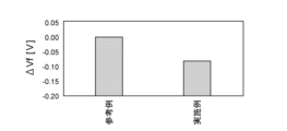
図9Aは、参考例に係る発光素子90および実施例に係る発光素子10の順方向電圧Vfと基準となる順方向電圧Vfrefとの差ΔVfを示すグラフである。
図9Bは、参考例に係る発光素子90および実施例に係る発光素子10の各出力Poを正規化した値Po/Porefを示すグラフである。
FIG. 9A is a graph showing the difference ΔVf between the forward voltage Vf of the light-emitting
FIG. 9B is a graph showing the normalized value Po/Poref of each output Po of the light-emitting
参考例に係る発光素子90および実施例に係る発光素子10の順方向電圧Vfをそれぞれ測定した。その結果を図9Aに示す。なお、図9Aの縦軸は、参考例における順方向電圧Vfを基準となる順方向電圧Vfrefとし、測定した各順方向電圧Vfから基準となる順方向電圧Vfrefを減算した値である。すなわち、ΔVf=Vf-Vfrefである。
The forward voltage Vf of the light-emitting
また、参考例および実施例に係る発光素子の出力Poをそれぞれ測定した。その結果を図9Bに示す。なお、図9Bの縦軸は、参考例における出力Poを基準となる出力Porefとし、測定した各出力Poを基準となる出力Porefで除算することにより、正規化した値である。 The output Po of the light-emitting element according to the reference example and the embodiment was also measured. The results are shown in FIG. 9B. Note that the vertical axis of FIG. 9B shows normalized values obtained by dividing each measured output Po by the reference output Poref, with the output Po in the reference example being the reference output Poref.
図9Aに示すように、実施例に係る発光素子10の順方向電圧Vfは、参考例に係る発光素子90の順方向電圧Vfよりも低い。そして、図9Bに示すように、実施例に係る発光素子10の出力Poは、参考例に係る発光素子90の出力Poと概ね同等である。したがって、第2n側半導体層121に第1層121a、第2層121b、および第4層121cを配置することで、出力Poを維持しつつ、順方向電圧Vfを低減できることが分かった。
As shown in FIG. 9A, the forward voltage Vf of the light-emitting
10、90 :発光素子
11 :基板
12 :半導体構造体
13 :n側電極
14 :p側電極
110 :第1発光部
111 :下地層
112 :第1n側半導体層
112s1 :第1面
112s2 :第2面
112s3 :第3面
113 :第1活性層
114 :第1p側半導体層
120 :第2発光部
121、921:第2n側半導体層
121a :第1層
121b :第2層
121c :第4層
121d :第3層
121e :第5層
122 :第2活性層
123 :第2p側半導体層
921a :最下層
e :電子
t1、t2、t3、t4、t91:厚み
10, 90: Light emitting element 11: Substrate 12: Semiconductor structure 13: n-side electrode 14: p-side electrode 110: First light emitting portion 111: Underlying layer 112: First n-side semiconductor layer 112s1: First surface 112s2: Second surface 112s3: Third surface 113: First active layer 114: First p-side semiconductor layer 120: Second
Claims (7)
前記第2n側半導体層は、下方から上方に向かって順に、第1層と、第2層と、第3層と、を有し、
前記第1層は、インジウムおよびガリウムを含み、第1n型不純物濃度を有し、
前記第2層は、インジウムおよびガリウムを含み、前記第1n型不純物濃度よりも低い第2n型不純物濃度を有し、
前記第2層におけるインジウムの組成比の値は、前記第1層におけるインジウムの組成比の値よりも小さく、
前記第2層の厚みは、前記第1層の厚みよりも大きく、
前記第3層は、ガリウムを含み、前記第2n型不純物濃度よりも低い第3n型不純物濃度を有する、発光素子。 The semiconductor device includes, in order from bottom to top, a first n-side semiconductor layer, a first active layer, a first p-side semiconductor layer, a second n-side semiconductor layer that forms a tunnel junction with the first p-side semiconductor layer, a second active layer, and a second p-side semiconductor layer, each of which is made of a nitride semiconductor ;
the second n-side semiconductor layer has, in order from bottom to top, a first layer, a second layer, and a third layer,
the first layer comprises indium and gallium and has a first n-type impurity concentration;
the second layer includes indium and gallium and has a second n-type impurity concentration lower than the first n-type impurity concentration;
a value of the indium composition ratio in the second layer is smaller than a value of the indium composition ratio in the first layer;
The thickness of the second layer is greater than the thickness of the first layer,
the third layer contains gallium and has a third n-type impurity concentration lower than the second n-type impurity concentration.
前記第4層は、アルミニウムおよびガリウムを含み、前記第3n型不純物濃度よりも高い第4n型不純物濃度を有する、請求項1または2に記載の発光素子。 the second n-side semiconductor layer further includes a fourth layer disposed between the second layer and the third layer,
The light-emitting device according to claim 1 , wherein the fourth layer contains aluminum and gallium and has a fourth n-type impurity concentration higher than the third n-type impurity concentration.
前記第3層は、n型不純物がドープされた窒化ガリウム層である、請求項1~6のいずれか1つに記載の発光素子。 the first layer and the second layer are indium gallium nitride layers doped with n-type impurities;
7. The light emitting device according to claim 1, wherein the third layer is a gallium nitride layer doped with an n-type impurity.
Priority Applications (2)
| Application Number | Priority Date | Filing Date | Title |
|---|---|---|---|
| JP2021206191A JP7526915B2 (en) | 2021-12-20 | 2021-12-20 | Light emitting element |
| US18/064,459 US12382753B2 (en) | 2021-12-20 | 2022-12-12 | Light-emitting element |
Applications Claiming Priority (1)
| Application Number | Priority Date | Filing Date | Title |
|---|---|---|---|
| JP2021206191A JP7526915B2 (en) | 2021-12-20 | 2021-12-20 | Light emitting element |
Publications (2)
| Publication Number | Publication Date |
|---|---|
| JP2023091442A JP2023091442A (en) | 2023-06-30 |
| JP7526915B2 true JP7526915B2 (en) | 2024-08-02 |
Family
ID=86769050
Family Applications (1)
| Application Number | Title | Priority Date | Filing Date |
|---|---|---|---|
| JP2021206191A Active JP7526915B2 (en) | 2021-12-20 | 2021-12-20 | Light emitting element |
Country Status (2)
| Country | Link |
|---|---|
| US (1) | US12382753B2 (en) |
| JP (1) | JP7526915B2 (en) |
Citations (9)
| Publication number | Priority date | Publication date | Assignee | Title |
|---|---|---|---|---|
| US20050067627A1 (en) | 2003-09-17 | 2005-03-31 | Guangdi Shen | High efficiency multi-active layer tunnel regenerated white light emitting diode |
| JP2008130877A (en) | 2006-11-22 | 2008-06-05 | Sharp Corp | Manufacturing method of nitride semiconductor light emitting device |
| JP2010251804A (en) | 2001-12-21 | 2010-11-04 | Xerox Corp | Structure of semiconductor laser |
| JP2011040784A (en) | 2010-10-21 | 2011-02-24 | Sharp Corp | Nitride semiconductor light emitting device |
| JP2013062528A (en) | 2005-10-29 | 2013-04-04 | Samsung Electronics Co Ltd | Semiconductor device and method of fabricating the same |
| JP2013122950A (en) | 2011-12-09 | 2013-06-20 | Toyoda Gosei Co Ltd | Group iii nitride semiconductor light-emitting element |
| JP2019517144A (en) | 2016-05-20 | 2019-06-20 | ルミレッズ リミテッド ライアビリティ カンパニー | Method of forming p-type layer of light emitting device |
| JP2019522356A (en) | 2016-05-20 | 2019-08-08 | ルミレッズ リミテッド ライアビリティ カンパニー | Method for using remote plasma chemical vapor deposition and sputtering deposition to grow layers in light emitting devices |
| JP2021158291A (en) | 2020-03-30 | 2021-10-07 | 日亜化学工業株式会社 | Nitride semiconductor device manufacturing method |
Family Cites Families (9)
| Publication number | Priority date | Publication date | Assignee | Title |
|---|---|---|---|---|
| US5777350A (en) | 1994-12-02 | 1998-07-07 | Nichia Chemical Industries, Ltd. | Nitride semiconductor light-emitting device |
| US6900465B2 (en) | 1994-12-02 | 2005-05-31 | Nichia Corporation | Nitride semiconductor light-emitting device |
| JP3538275B2 (en) * | 1995-02-23 | 2004-06-14 | 日亜化学工業株式会社 | Nitride semiconductor light emitting device |
| CN100350641C (en) | 1995-11-06 | 2007-11-21 | 日亚化学工业株式会社 | Nitride semiconductor device |
| JP2900990B2 (en) * | 1995-11-24 | 1999-06-02 | 日亜化学工業株式会社 | Nitride semiconductor light emitting device |
| US6822991B2 (en) | 2002-09-30 | 2004-11-23 | Lumileds Lighting U.S., Llc | Light emitting devices including tunnel junctions |
| US7612362B2 (en) | 2006-11-22 | 2009-11-03 | Sharp Kabushiki Kaisha | Nitride semiconductor light emitting device |
| JP2008130878A (en) | 2006-11-22 | 2008-06-05 | Sharp Corp | Nitride semiconductor light emitting device |
| JP7104519B2 (en) | 2018-01-11 | 2022-07-21 | 日機装株式会社 | Nitride semiconductor light emitting device |
-
2021
- 2021-12-20 JP JP2021206191A patent/JP7526915B2/en active Active
-
2022
- 2022-12-12 US US18/064,459 patent/US12382753B2/en active Active
Patent Citations (9)
| Publication number | Priority date | Publication date | Assignee | Title |
|---|---|---|---|---|
| JP2010251804A (en) | 2001-12-21 | 2010-11-04 | Xerox Corp | Structure of semiconductor laser |
| US20050067627A1 (en) | 2003-09-17 | 2005-03-31 | Guangdi Shen | High efficiency multi-active layer tunnel regenerated white light emitting diode |
| JP2013062528A (en) | 2005-10-29 | 2013-04-04 | Samsung Electronics Co Ltd | Semiconductor device and method of fabricating the same |
| JP2008130877A (en) | 2006-11-22 | 2008-06-05 | Sharp Corp | Manufacturing method of nitride semiconductor light emitting device |
| JP2011040784A (en) | 2010-10-21 | 2011-02-24 | Sharp Corp | Nitride semiconductor light emitting device |
| JP2013122950A (en) | 2011-12-09 | 2013-06-20 | Toyoda Gosei Co Ltd | Group iii nitride semiconductor light-emitting element |
| JP2019517144A (en) | 2016-05-20 | 2019-06-20 | ルミレッズ リミテッド ライアビリティ カンパニー | Method of forming p-type layer of light emitting device |
| JP2019522356A (en) | 2016-05-20 | 2019-08-08 | ルミレッズ リミテッド ライアビリティ カンパニー | Method for using remote plasma chemical vapor deposition and sputtering deposition to grow layers in light emitting devices |
| JP2021158291A (en) | 2020-03-30 | 2021-10-07 | 日亜化学工業株式会社 | Nitride semiconductor device manufacturing method |
Non-Patent Citations (6)
| Title |
|---|
| Joachim PIPREK,Origin of InGaN/GaN light-emitting diode efficiency improvements using tunnel-junction-cascaded active regions,Applied Physics Letters,米国,2014年02月,Vol.104,p.051118-1 - p.051118-4 |
| P. LI et al.,Demonstration of high efficiency cascaded blue and green micro-light-emitting diodes with independent junction control,Applied Physics Letters,米国,2021年06月,Vol.118,p.261104-1 - p.261104-4 |
| S.J. CHANG et al.,Cascaded GaN Light-Emitting Diodes With Hybrid Tunnel Junction Layers,IEEE JOURNAL OF QUANTUM ELECTRONICS,米国,2015年08月,VOL.51, NO.8,p.3300505 |
| TURSKI Henryk et al.,Polarization control in nitride quantum well light emitters enabled by bottom tunnel-junctions,Journal of Applied Physics,米国,2019年05月,Vol.125,p.203104-1 - p.203104-11 |
| ZHANG YUEWEI et al.,Design and demonstration of ultra-wide bandgap AlGaN tunnel junctions,APPLIED PHYSICS LETTERS,米国,2016年09月,Vol.109,p.121102-1 - p.121102-5 |
| ZHANG Yuewei et al.,Tunnel-injected sub 290nm ultra-violet light emitting diodes with 2.8% external quantum efficiency,APPLIED PHYSICS LETTERS,米国,2018年02月,Vol.112,p.071107-1 - p.071107-4 |
Also Published As
| Publication number | Publication date |
|---|---|
| US12382753B2 (en) | 2025-08-05 |
| JP2023091442A (en) | 2023-06-30 |
| US20230197897A1 (en) | 2023-06-22 |
Similar Documents
| Publication | Publication Date | Title |
|---|---|---|
| JP5737111B2 (en) | Group III nitride semiconductor light emitting device | |
| JP7481618B2 (en) | Method for manufacturing nitride semiconductor device | |
| US12376426B2 (en) | Nitride semiconductor light-emitting element | |
| US20240072209A1 (en) | Light-emitting element | |
| US8659041B2 (en) | Nitride semiconductor light emitting diode | |
| CN101330121A (en) | Manufacturing method of nitride semiconductor light emitting device | |
| CN102272952A (en) | Optoelectronic semiconductor component | |
| US12501746B2 (en) | Light-emitting element including p-side layer with first and second layers having different p-type impurity concentrations and method for manufacturing same | |
| JP7526915B2 (en) | Light emitting element | |
| US12288832B2 (en) | Method for manufacturing light-emitting element | |
| JP7526916B2 (en) | Light emitting element | |
| JP7373107B2 (en) | Manufacturing method of light emitting device | |
| JP6192722B2 (en) | Optoelectronic semiconductor body and optoelectronic semiconductor chip | |
| US12501741B2 (en) | Method for manufacturing light-emitting element | |
| US20240332450A1 (en) | Nitride semiconductor light-emitting element | |
| JP2023080013A (en) | Light-emitting element and method for manufacturing light-emitting element | |
| US12527140B2 (en) | Method of manufacturing light emitting element | |
| TW202226610A (en) | Nitride semiconductor element and method of manufacturing nitride semiconductor element | |
| JP2023040785A (en) | Method for manufacturing light-emitting element |
Legal Events
| Date | Code | Title | Description |
|---|---|---|---|
| A621 | Written request for application examination |
Free format text: JAPANESE INTERMEDIATE CODE: A621 Effective date: 20230117 |
|
| A977 | Report on retrieval |
Free format text: JAPANESE INTERMEDIATE CODE: A971007 Effective date: 20231108 |
|
| A131 | Notification of reasons for refusal |
Free format text: JAPANESE INTERMEDIATE CODE: A131 Effective date: 20231109 |
|
| A601 | Written request for extension of time |
Free format text: JAPANESE INTERMEDIATE CODE: A601 Effective date: 20231127 |
|
| A521 | Request for written amendment filed |
Free format text: JAPANESE INTERMEDIATE CODE: A523 Effective date: 20240306 |
|
| TRDD | Decision of grant or rejection written | ||
| A01 | Written decision to grant a patent or to grant a registration (utility model) |
Free format text: JAPANESE INTERMEDIATE CODE: A01 Effective date: 20240620 |
|
| A61 | First payment of annual fees (during grant procedure) |
Free format text: JAPANESE INTERMEDIATE CODE: A61 Effective date: 20240703 |
|
| R150 | Certificate of patent or registration of utility model |
Ref document number: 7526915 Country of ref document: JP Free format text: JAPANESE INTERMEDIATE CODE: R150 |