JP6881102B2 - Connection structure of circuit board and connector for board and connector for board - Google Patents
Connection structure of circuit board and connector for board and connector for board Download PDFInfo
- Publication number
- JP6881102B2 JP6881102B2 JP2017131868A JP2017131868A JP6881102B2 JP 6881102 B2 JP6881102 B2 JP 6881102B2 JP 2017131868 A JP2017131868 A JP 2017131868A JP 2017131868 A JP2017131868 A JP 2017131868A JP 6881102 B2 JP6881102 B2 JP 6881102B2
- Authority
- JP
- Japan
- Prior art keywords
- shield
- unshielded
- board
- tab
- connector
- Prior art date
- Legal status (The legal status is an assumption and is not a legal conclusion. Google has not performed a legal analysis and makes no representation as to the accuracy of the status listed.)
- Active
Links
Images


Classifications
-
- H—ELECTRICITY
- H01—ELECTRIC ELEMENTS
- H01R—ELECTRICALLY-CONDUCTIVE CONNECTIONS; STRUCTURAL ASSOCIATIONS OF A PLURALITY OF MUTUALLY-INSULATED ELECTRICAL CONNECTING ELEMENTS; COUPLING DEVICES; CURRENT COLLECTORS
- H01R13/00—Details of coupling devices of the kinds covered by groups H01R12/70 or H01R24/00 - H01R33/00
- H01R13/648—Protective earth or shield arrangements on coupling devices, e.g. anti-static shielding
- H01R13/658—High frequency shielding arrangements, e.g. against EMI [Electro-Magnetic Interference] or EMP [Electro-Magnetic Pulse]
- H01R13/6591—Specific features or arrangements of connection of shield to conductive members
- H01R13/6594—Specific features or arrangements of connection of shield to conductive members the shield being mounted on a PCB and connected to conductive members
-
- H—ELECTRICITY
- H01—ELECTRIC ELEMENTS
- H01R—ELECTRICALLY-CONDUCTIVE CONNECTIONS; STRUCTURAL ASSOCIATIONS OF A PLURALITY OF MUTUALLY-INSULATED ELECTRICAL CONNECTING ELEMENTS; COUPLING DEVICES; CURRENT COLLECTORS
- H01R13/00—Details of coupling devices of the kinds covered by groups H01R12/70 or H01R24/00 - H01R33/00
- H01R13/40—Securing contact members in or to a base or case; Insulating of contact members
- H01R13/42—Securing in a demountable manner
- H01R13/422—Securing in resilient one-piece base or case, e.g. by friction; One-piece base or case formed with resilient locking means
-
- H—ELECTRICITY
- H01—ELECTRIC ELEMENTS
- H01R—ELECTRICALLY-CONDUCTIVE CONNECTIONS; STRUCTURAL ASSOCIATIONS OF A PLURALITY OF MUTUALLY-INSULATED ELECTRICAL CONNECTING ELEMENTS; COUPLING DEVICES; CURRENT COLLECTORS
- H01R12/00—Structural associations of a plurality of mutually-insulated electrical connecting elements, specially adapted for printed circuits, e.g. printed circuit boards [PCB], flat or ribbon cables, or like generally planar structures, e.g. terminal strips, terminal blocks; Coupling devices specially adapted for printed circuits, flat or ribbon cables, or like generally planar structures; Terminals specially adapted for contact with, or insertion into, printed circuits, flat or ribbon cables, or like generally planar structures
- H01R12/50—Fixed connections
- H01R12/51—Fixed connections for rigid printed circuits or like structures
- H01R12/55—Fixed connections for rigid printed circuits or like structures characterised by the terminals
- H01R12/57—Fixed connections for rigid printed circuits or like structures characterised by the terminals surface mounting terminals
-
- H—ELECTRICITY
- H01—ELECTRIC ELEMENTS
- H01R—ELECTRICALLY-CONDUCTIVE CONNECTIONS; STRUCTURAL ASSOCIATIONS OF A PLURALITY OF MUTUALLY-INSULATED ELECTRICAL CONNECTING ELEMENTS; COUPLING DEVICES; CURRENT COLLECTORS
- H01R12/00—Structural associations of a plurality of mutually-insulated electrical connecting elements, specially adapted for printed circuits, e.g. printed circuit boards [PCB], flat or ribbon cables, or like generally planar structures, e.g. terminal strips, terminal blocks; Coupling devices specially adapted for printed circuits, flat or ribbon cables, or like generally planar structures; Terminals specially adapted for contact with, or insertion into, printed circuits, flat or ribbon cables, or like generally planar structures
- H01R12/70—Coupling devices
- H01R12/71—Coupling devices for rigid printing circuits or like structures
- H01R12/712—Coupling devices for rigid printing circuits or like structures co-operating with the surface of the printed circuit or with a coupling device exclusively provided on the surface of the printed circuit
- H01R12/716—Coupling device provided on the PCB
-
- H—ELECTRICITY
- H01—ELECTRIC ELEMENTS
- H01R—ELECTRICALLY-CONDUCTIVE CONNECTIONS; STRUCTURAL ASSOCIATIONS OF A PLURALITY OF MUTUALLY-INSULATED ELECTRICAL CONNECTING ELEMENTS; COUPLING DEVICES; CURRENT COLLECTORS
- H01R12/00—Structural associations of a plurality of mutually-insulated electrical connecting elements, specially adapted for printed circuits, e.g. printed circuit boards [PCB], flat or ribbon cables, or like generally planar structures, e.g. terminal strips, terminal blocks; Coupling devices specially adapted for printed circuits, flat or ribbon cables, or like generally planar structures; Terminals specially adapted for contact with, or insertion into, printed circuits, flat or ribbon cables, or like generally planar structures
- H01R12/70—Coupling devices
- H01R12/71—Coupling devices for rigid printing circuits or like structures
- H01R12/72—Coupling devices for rigid printing circuits or like structures coupling with the edge of the rigid printed circuits or like structures
- H01R12/722—Coupling devices for rigid printing circuits or like structures coupling with the edge of the rigid printed circuits or like structures coupling devices mounted on the edge of the printed circuits
- H01R12/724—Coupling devices for rigid printing circuits or like structures coupling with the edge of the rigid printed circuits or like structures coupling devices mounted on the edge of the printed circuits containing contact members forming a right angle
-
- H—ELECTRICITY
- H05—ELECTRIC TECHNIQUES NOT OTHERWISE PROVIDED FOR
- H05K—PRINTED CIRCUITS; CASINGS OR CONSTRUCTIONAL DETAILS OF ELECTRIC APPARATUS; MANUFACTURE OF ASSEMBLAGES OF ELECTRICAL COMPONENTS
- H05K1/00—Printed circuits
- H05K1/02—Details
- H05K1/0286—Programmable, customizable or modifiable circuits
- H05K1/0295—Programmable, customizable or modifiable circuits adapted for choosing between different types or different locations of mounted components
-
- H—ELECTRICITY
- H01—ELECTRIC ELEMENTS
- H01R—ELECTRICALLY-CONDUCTIVE CONNECTIONS; STRUCTURAL ASSOCIATIONS OF A PLURALITY OF MUTUALLY-INSULATED ELECTRICAL CONNECTING ELEMENTS; COUPLING DEVICES; CURRENT COLLECTORS
- H01R13/00—Details of coupling devices of the kinds covered by groups H01R12/70 or H01R24/00 - H01R33/00
- H01R13/648—Protective earth or shield arrangements on coupling devices, e.g. anti-static shielding
- H01R13/658—High frequency shielding arrangements, e.g. against EMI [Electro-Magnetic Interference] or EMP [Electro-Magnetic Pulse]
- H01R13/6581—Shield structure
-
- H—ELECTRICITY
- H01—ELECTRIC ELEMENTS
- H01R—ELECTRICALLY-CONDUCTIVE CONNECTIONS; STRUCTURAL ASSOCIATIONS OF A PLURALITY OF MUTUALLY-INSULATED ELECTRICAL CONNECTING ELEMENTS; COUPLING DEVICES; CURRENT COLLECTORS
- H01R2103/00—Two poles
-
- H—ELECTRICITY
- H05—ELECTRIC TECHNIQUES NOT OTHERWISE PROVIDED FOR
- H05K—PRINTED CIRCUITS; CASINGS OR CONSTRUCTIONAL DETAILS OF ELECTRIC APPARATUS; MANUFACTURE OF ASSEMBLAGES OF ELECTRICAL COMPONENTS
- H05K1/00—Printed circuits
- H05K1/02—Details
- H05K1/0213—Electrical arrangements not otherwise provided for
- H05K1/0216—Reduction of cross-talk, noise or electromagnetic interference
- H05K1/0218—Reduction of cross-talk, noise or electromagnetic interference by printed shielding conductors, ground planes or power plane
-
- H—ELECTRICITY
- H05—ELECTRIC TECHNIQUES NOT OTHERWISE PROVIDED FOR
- H05K—PRINTED CIRCUITS; CASINGS OR CONSTRUCTIONAL DETAILS OF ELECTRIC APPARATUS; MANUFACTURE OF ASSEMBLAGES OF ELECTRICAL COMPONENTS
- H05K1/00—Printed circuits
- H05K1/02—Details
- H05K1/11—Printed elements for providing electric connections to or between printed circuits
- H05K1/111—Pads for surface mounting, e.g. lay-out
-
- H—ELECTRICITY
- H05—ELECTRIC TECHNIQUES NOT OTHERWISE PROVIDED FOR
- H05K—PRINTED CIRCUITS; CASINGS OR CONSTRUCTIONAL DETAILS OF ELECTRIC APPARATUS; MANUFACTURE OF ASSEMBLAGES OF ELECTRICAL COMPONENTS
- H05K2201/00—Indexing scheme relating to printed circuits covered by H05K1/00
- H05K2201/10—Details of components or other objects attached to or integrated in a printed circuit board
- H05K2201/10007—Types of components
- H05K2201/10189—Non-printed connector
Landscapes
- Engineering & Computer Science (AREA)
- Microelectronics & Electronic Packaging (AREA)
- Coupling Device And Connection With Printed Circuit (AREA)
- Details Of Connecting Devices For Male And Female Coupling (AREA)
Description
本発明は、回路基板と基板用コネクタの接続構造及び基板用コネクタに関するものである。 The present invention relates to a connection structure between a circuit board and a connector for a board and a connector for a board.
特許文献1には、回路基板に取り付けられる基板用コネクタが開示されている。基板用コネクタは、回路基板に固定される端子保持部材と、端子保持部材に貫通状態で取り付けられた複数の端子金具とを備えている。端子金具は、端子保持部材のフード部内に収容されてワイヤーハーネスに接続されるハーネス側接続部と、端子保持部材の後方に露出して回路基板の回路に溶接により接続される基板用接続部とを有している。
上記の基板用コネクタは、複数の端子金具が左右方向に所定ピッチで並列配置されている。端子金具の適正な並列ピッチは、端子金具が外導体で包囲されるシールド用の基板用コネクタと、端子金具がツイストペア線に接続される非シールド用の基板用コネクタとで異なる。したがって、回路基板の導体パターンのうち基板用接続部が接続されるパッドの間隔も、シールド用の回路基板と非シール用の回路基板とで異なる。そのため、シールド用の回路基板と非シールド用の回路基板に対応するためには、パッドの間隔が異なる2種類の回路基板を用意する必要があった。 In the above-mentioned board connector, a plurality of terminal fittings are arranged in parallel in the left-right direction at a predetermined pitch. The proper parallel pitch of the terminal fittings differs between the shielded board connector in which the terminal fittings are surrounded by the outer conductor and the unshielded board connector in which the terminal fittings are connected to the twisted pair wire. Therefore, the distance between the pads to which the board connection portion is connected in the conductor pattern of the circuit board is also different between the shield circuit board and the non-seal circuit board. Therefore, in order to support a shielded circuit board and a non-shielded circuit board, it is necessary to prepare two types of circuit boards having different pad spacings.
本発明は上記のような事情に基づいて完成されたものであって、回路基板の種類数を増やさずに済むようにすることを目的とする。 The present invention has been completed based on the above circumstances, and an object of the present invention is to avoid increasing the number of types of circuit boards.
第1の発明にかかる回路基板と基板用コネクタの接続構造は、
回路基板と、
前記回路基板に対し選択的に取付け可能なシールド用基板用コネクタと非シールド用基板用コネクタとを備え、
前記シールド用基板用コネクタは、前記回路基板の上面に取付け可能なシールド用端子保持部材と、前記シールド用端子保持部材に貫通状態で保持されたシールド用タブ状接続部と、前記シールド用端子保持部材の外部において前記回路基板のパッドに接続されるシールド用基板接続部とを有する左右一対のシールド用端子金具とを備えて構成され、
前記非シールド用基板用コネクタは、前記回路基板の上面に取付け可能な非シールド用端子保持部材と、前記非シールド用端子保持部材に貫通状態で保持された非シールド用タブ状接続部と、前記非シールド用端子保持部材の外部において前記回路基板の前記パッドに接続される非シールド用基板接続部とを有する左右一対の非シールド用端子金具とを備えて構成され、
前記一対のシールド用端子金具は、前記シールド用タブ状接続部のピッチが前記シールド用基板接続部のピッチより広く、
前記一対の非シールド用端子金具は、前記非シールド用タブ状接続部のピッチが前記非シールド用基板接続部のピッチより狭く、
前記シールド用基板接続部のピッチと前記非シールド用基板接続部のピッチが概ね同じであるところに特徴を有する。
The connection structure between the circuit board and the connector for the board according to the first invention is as follows.
With the circuit board
It is provided with a shield board connector and a non-shield board connector that can be selectively attached to the circuit board.
The shield board connector includes a shield terminal holding member that can be attached to the upper surface of the circuit board, a shield tab-shaped connection portion that is held through the shield terminal holding member in a penetrating state, and the shield terminal holding. It is configured to include a pair of left and right shield terminal fittings having a shield board connection portion connected to the pad of the circuit board outside the member.
The unshielded substrate connector includes an unshielded terminal holding member that can be attached to the upper surface of the circuit board, an unshielded tab-shaped connecting portion that is held through the unshielded terminal holding member in a penetrating state, and the above. It is configured to include a pair of left and right unshielded terminal fittings having an unshielded board connection portion connected to the pad of the circuit board outside the unshielded terminal holding member.
In the pair of shield terminal fittings, the pitch of the shield tab-shaped connection portion is wider than the pitch of the shield substrate connection portion.
In the pair of unshielded terminal fittings, the pitch of the unshielded tab-shaped connection portion is narrower than the pitch of the unshielded substrate connection portion.
The feature is that the pitch of the shielded substrate connecting portion and the pitch of the unshielded substrate connecting portion are substantially the same.
第2の発明にかかる基板用コネクタは、
回路基板の上面に取り付け可能な端子保持部材と、
前記端子保持部材に貫通状態で保持されたタブ状接続部と、前記端子保持部材の外部において前記回路基板のパッドに接続される基板接続部とを有する左右一対の端子金具とを備え、
前記一対の端子金具は、前記タブ状接続部のピッチと前記基板接続部のピッチとが異なっているところに特徴を有する。
The board connector according to the second invention is
A terminal holding member that can be attached to the top surface of the circuit board,
It is provided with a pair of left and right terminal fittings having a tab-shaped connecting portion held in a penetrating state by the terminal holding member and a board connecting portion connected to a pad of the circuit board outside the terminal holding member.
The pair of terminal fittings is characterized in that the pitch of the tab-shaped connecting portion and the pitch of the substrate connecting portion are different.
第1の発明によれば、シールド用基板接続部のピッチと非シールド用基板接続部のピッチが概ね同じ寸法なので、シールド用の回路基板のパッドの間隔と、非シールド用の回路基板のパッドの間隔とを同じピッチに設定することができる。これにより、シールド用基板用コネクタと非シールド用基板用コネクタとで回路基板を共用化することができる。 According to the first invention, since the pitch of the shielded substrate connection portion and the pitch of the unshielded substrate connection portion are approximately the same dimensions, the distance between the pads of the shielded circuit board and the pad of the unshielded circuit board The interval can be set to the same pitch. As a result, the circuit board can be shared between the shielded board connector and the non-shielded board connector.
第2の発明によれば、シールド用の基板用コネクタでは、タブ状接続部のピッチが基板接続部のピッチより大きくなるように一対の端子金具を端子保持部材に取り付け、非シールド用の基板用コネクタでは、タブ状接続部のピッチが基板接続部のピッチより小さくなるように一対の端子金具を端子保持部材に取り付ける。ここで、シールド用の基板接続部のピッチと非シールド用の基板接続部のピッチが概ね同じ寸法となるようにすれば、シールド用の基板用コネクタと非シールド用の基板用コネクタとで回路基板を共用化することができる。 According to the second invention, in the shielded substrate connector, a pair of terminal fittings are attached to the terminal holding member so that the pitch of the tab-shaped connecting portion is larger than the pitch of the substrate connecting portion, and the connector is used for a non-shielded substrate. In the connector, a pair of terminal fittings are attached to the terminal holding member so that the pitch of the tab-shaped connecting portion is smaller than the pitch of the board connecting portion. Here, if the pitch of the shielded board connection portion and the pitch of the unshielded board connection portion have substantially the same dimensions, the circuit board can be formed between the shielded board connector and the unshielded board connector. Can be shared.
第1の発明は、前記シールド用タブ状接続部のピッチをPw、前記非シールド用タブ状接続部のピッチをPn、前記シールド用基板接続部のピッチ及び前記非シールド用基板接続部のピッチをPoとしたときに、Po=Pw/2+Pn/2としてもよい。この構成によれば、シールド用タブ状接続部のピッチPwとシールド用基板接続部のピッチPoの寸法差と、非シールド用タブ状接続部のピッチPnと非シールド用基板接続部のピッチPoの寸法差とが同じ寸法となるので、一対のシールド用端子金具と一対の非シールド用端子金具を共用化することができる。 In the first invention, the pitch of the shield tab-shaped connection portion is Pw, the pitch of the non-shield tab-shaped connection portion is Pn, the pitch of the shield substrate connection portion and the pitch of the non-shield substrate connection portion. When Po is set, Po = Pw / 2 + Pn / 2 may be set. According to this configuration, the dimensional difference between the pitch Pw of the shield tab-shaped connection portion and the pitch Po of the shield board connection portion, and the pitch Pn of the non-shield tab-shaped connection portion and the pitch Po of the non-shield board connection portion. Since the dimensional difference is the same, the pair of shielded terminal fittings and the pair of unshielded terminal fittings can be shared.
第1の発明は、前記シールド用端子金具は、前記シールド用タブ状接続部の後端と前記シールド用基板接続部とを繋ぐシールド用脚部を有しており、前記シールド用脚部が、前記シールド用タブ状接続部に対し左右方向において同心状に配されていてもよい。この構成によれば、左右一対のシールド用端子金具の間隔に起因する高い通信性能が回路基板の近傍まで維持される。 In the first invention, the shield terminal fitting has a shield leg portion that connects the rear end of the shield tab-shaped connection portion and the shield substrate connection portion, and the shield leg portion is formed by the shield leg portion. It may be arranged concentrically in the left-right direction with respect to the tab-shaped connecting portion for shielding. According to this configuration, high communication performance due to the distance between the pair of left and right shield terminal fittings is maintained up to the vicinity of the circuit board.
第1の発明は、前記非シールド用端子金具は、前記非シールド用タブ状接続部の後端と前記非シールド用基板接続部とを繋ぐ非シールド用脚部を有しており、前記非シールド用脚部が、前記非シールド用タブ状接続部に対し左右方向において同心状に配されていてもよい。この構成によれば、左右一対の非シールド用端子金具の間隔に起因する高い通信性能が回路基板の近傍まで維持される。 In the first invention, the unshielded terminal fitting has an unshielded leg portion that connects the rear end of the unshielded tab-shaped connecting portion and the unshielded substrate connecting portion, and the unshielded leg portion. The legs may be arranged concentrically in the left-right direction with respect to the unshielded tab-shaped connecting portion. According to this configuration, high communication performance due to the distance between the pair of left and right unshielded terminal fittings is maintained up to the vicinity of the circuit board.
第2の発明は、前記端子金具は、前記タブ状接続部の後端と前記基板接続部とを繋ぐ脚部を有しており、前記脚部が、前記タブ状接続部に対し左右方向において同心状に配されていてもよい。この構成によれば、左右一対の端子金具の間隔に起因する高い通信性能が回路基板の近傍まで維持される。 In the second invention, the terminal fitting has a leg portion that connects the rear end of the tab-shaped connecting portion and the board connecting portion, and the leg portion is in the left-right direction with respect to the tab-shaped connecting portion. They may be arranged concentrically. According to this configuration, high communication performance due to the distance between the pair of left and right terminal fittings is maintained up to the vicinity of the circuit board.
<実施例1>
以下、本発明を具体化した実施例1を図1〜図8を参照して説明する。尚、以下の説明において、前後の方向については、図3,7における上方及び図4,8における左方を前方と定義する。上下の方向については、図1,2,4,5,6,8にあらわれる向きを、そのまま上方、下方と定義する。左右の方向については、図2,3,6,7にあらわれる向きを、そのまま左方、右方と定義する。
<Example 1>
Hereinafter, Example 1 embodying the present invention will be described with reference to FIGS. 1 to 8. In the following description, the front-back direction is defined as the upper side in FIGS. 3 and 7 and the left side in FIGS. 4 and 8 as the front direction. As for the vertical direction, the directions appearing in FIGS. 1, 2, 4, 5, 6 and 8 are defined as upward and downward as they are. Regarding the left-right direction, the directions appearing in FIGS. 2, 3, 6 and 7 are defined as left and right as they are.
本実施例1の接続構造は、イーサネット(登録商標)の高速通信回路に用いられるものである。この接続構造は、シールド用と非シールド用とで共通の回路基板10と、シールド用基板用コネクタ20(請求項に記載の基板用コネクタ)と、非シールド用基板用コネクタ35(請求項に記載の基板用コネクタ)とを備えて構成されている。回路基板10には、シールド用基板用コネクタ20と非シールド用基板用コネクタ35のいずれか一方のみが取り付けられる。
The connection structure of the first embodiment is used for a high-speed communication circuit of Ethernet (registered trademark). This connection structure includes a
<回路基板10>
回路基板10は水平な向きに配され、回路基板10の上面には、導体パターン(図示省略)が印刷により形成されている。図3に示すように、回路基板10の前端縁よりも後方の領域には、導体パターンを構成する左右対称な一対のパッド11が配されている。一対のパッド11の平面視形状は、前後方向に細長い略長方形をなす。一対のパッド11は、所定のピッチPoで左右に並ぶように配置されている。
<
The
回路基板10の上面のうち一対のパッド11より前方の領域は、シールド用基板用コネクタ20または非シールド用基板用コネクタ35を配置するための固定スペースとなっている。回路基板10の導体パターン及び回路基板10に実装される電子部品(図示省略)は、シールド用基板用コネクタ20と非シールド用基板用コネクタ35とで共通となっている。回路基板10は、電磁シールドされた筐体(図示省略)内に収容されている。
The area of the upper surface of the
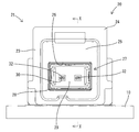
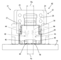
<シールド用基板用コネクタ20>
シールド用基板用コネクタ20は、図1〜4に示すように、シールド用端子保持部材21と、左右対称な一対の端子金具31(請求項に記載のシールド用端子金具及び非シールド用端子金具)とを備えて構成されている。シールド用端子保持部材21は、機能的には、回路基板10の上面に対して略鉛直をなす壁状のシールド用端子貫通部22と、シールド用端子貫通部22の外周縁から前方へ角筒状に延出したシールド用フード部23とを備えて構成されている。シールド用端子保持部材21は、部品構成的には、合成樹脂製の絶縁ハウジング24と、外導体28と、誘電体29とを組み付けて構成されている。
<Connector for
As shown in FIGS. 1 to 4, the
絶縁ハウジング24は、シールド用端子貫通部22を構成するシールド用壁状本体部25と、シールド用壁状本体部25の外周縁から前方へ突出したシールド用フード部23とを有する単一部品である。シールド用壁状本体部25には、前後方向に貫通する取付孔26が形成されている。取付孔26には、シールド端子27が貫通状態で取り付けられている。
The insulating
シールド端子27は、側面視形状が略L字形に屈曲した角筒状の外導体28と、外導体28内の後端部に収容した誘電体29と、左右一対の端子金具31とを組み付けて構成されている。誘電体29には、前後方向に貫通する左右一対のシールド用圧入孔30が形成され、一対の端子金具31は、各シールド用圧入孔30を圧入状態で個別に貫通している。
The
シールド端子27のうち外導体28の後端部は取付孔26内に嵌合されている。シールド端子27のうち外導体28の前端側領域と端子金具31の前端側領域(タブ状接続部32の前端側領域)は、シールド用壁状本体部25から前方へ突出してシールド用フード部23内に収容されている。シールド用端子貫通部22は、シールド用壁状本体部25と誘電体29とを備えて構成されている。一対の端子金具31は、シールド用端子貫通部22を貫通した状態でシールド用端子保持部材21に保持されている。
The rear end of the
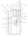
図2,3に示すように、一対の端子金具31は、左右対称な形状である。各端子金具31は、1本の細長い金属材料を曲げ加工して所定形状に成形したものである。図4に示すように、端子金具31は、タブ状接続部32(請求項に記載のシールド用タブ状接続部及び非シールド用タブ状接続部)と、脚部33(請求項に記載のシールド用脚部及び非シールド用脚部)と、基板接続部34(請求項に記載のシールド用基板接続部及び非シールド用基板接続部)とを備えている。
As shown in FIGS. 2 and 3, the pair of
タブ状接続部32は、前後方向(回路基板10の上面と平行な方向)に直線状に延びた形態であり、シールド用端子貫通部22のシールド用圧入孔30を前後方向に貫通している。タブ状接続部32の前端側領域は、シールド用端子貫通部22の前方へ突出してシールド用フード部23内に収容されている。タブ状接続部32の後端部は、シールド用端子貫通部22を構成する誘電体29の後方に突出し、外導体28の後端部で覆われている。
The tab-shaped connecting
脚部33は、タブ状接続部32の後端から略直角に下方(回路基板10に接近する方向)へ直線状に延出し、外導体28の後端部で覆われている。基板接続部34は、脚部33の下端から回路基板10の上面と略平行をなすように直線状に延出している。基板接続部34の幅寸法(左右方向の寸法)はパッド11の幅寸法よりも小さい。図3に示すように、平面視において、一対の基板接続部34は一対のパッド11と重なるように配され、各基板接続部34は左右方向においてパッド11の中央位置に配されている。基板接続部34は、パッド11の上面に対しリフローハンダにより導通可能に固着されている。
The
一対の端子金具31は、シールド用端子保持部材21に取り付けた状態で左右対称に配置されている。シールド用端子保持部材21に取り付けた状態における一対の端子金具31は、タブ状接続部32同士の左右方向のピッチPwが基板接続部34同士の左右方向のピッチPoより大きい寸法となっている。図2,3に示すように、平面視及び背面視において、タブ状接続部32と脚部33は、幅方向(左右方向)の中心が合致した同心の位置関係にある。基板接続部34の幅方向中心は、タブ状接続部32及び脚部33に対して左右いずれかに偏心した位置関係である。即ち、左側に位置する端子金具31ではタブ状接続部32と脚部33が基板接続部34よりも左方へ偏心し、右側に位置する端子金具31ではタブ状接続部32と脚部33が基板接続部34よりも右方へ偏心している。
The pair of
シールド用基板用コネクタ20には、シールドハーネス(図示省略)の端末部に取り付けたシールドコネクタ(図示省略)が嵌合される。シールドハーネスは、一対の非シールド電線を編組線等の筒状シールド部材で包囲し、各非シールド電線に雌端子金具を固着した形態である。一対の雌端子金具は、シールドコネクタ内に収容され、シールドコネクタを構成するシールドシェルで包囲されている。シールドコネクタをシールド用基板用コネクタ20のシールド用フード部23に嵌合すると、一対の雌端子金具が一対のタブ状接続部32に個別に接続されるとともに、シールドシェルが外導体28に接続される。
A shield connector (not shown) attached to the terminal portion of the shield harness (not shown) is fitted to the
上記のように左右両タブ状接続部32のピッチPwは基板接続部34のピッチPoより広いのであるが、これは、左右両タブ状接続部32間の間隔を、シールド端子27におけるタブ状接続部32と外導体28との距離に合わせたことによるものである。タブ状接続部32と外導体28との距離は、シールドコネクタにおける雌端子金具とシールドシェルとの距離とおおむね同じ寸法である。タブ状接続部32と外導体28との距離は、シールド機能を勘案して最適となるように設定されている。
As described above, the pitch Pw of the left and right tab-shaped connecting
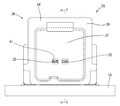
<非シールド用基板用コネクタ35>
非シールド用基板用コネクタ35は、図5〜8に示すように、非シールド用端子保持部材36と、左右対称な一対の端子金具31とを備えて構成されている。一対の端子金具31は、シールド用基板用コネクタ20を構成する一対の端子金具31と同じ部品を左右逆の配置となるように入れ換えたものである。非シールド用端子保持部材36は、全体形状としては、回路基板10の上面に対して略鉛直をなす壁状の非シールド用端子貫通部37と、非シールド用端子貫通部37の外周縁から前方へ角筒状に延出した非シールド用フード部38とを備えて構成されている。非シールド用端子保持部材36は、合成樹脂製のコネクタハウジング39からなる。
<
As shown in FIGS. 5 to 8, the
コネクタハウジング39は、非シールド用端子貫通部37を構成する非シールド用壁状本体部40と、非シールド用壁状本体部40の外周縁から前方へ突出した非シールド用フード部38とを有する単一部品である。非シールド用壁状本体部40には、前後方向に貫通する左右一対の非シールド用圧入孔41が形成されている。一対の端子金具31は、各非シールド用圧入孔41を圧入状態で個別に貫通した状態で非シールド用端子保持部材36に保持されている。
The
図6,7に示すように、非シールド用基板用コネクタ35における一対の端子金具31も、シールド用基板用コネクタ20と同様、左右対称な形状である。タブ状接続部32は、前後方向(回路基板10の上面と平行な方向)に直線状に延びた形態であり、非シールド用端子貫通部37の非シールド用圧入孔41を前後方向に貫通している。タブ状接続部32の前端側領域は、非シールド用端子貫通部37の前方へ突出して非シールド用フード部38内に収容されている。タブ状接続部32の後端部は、非シールド用端子貫通部37の後方に突出している。
As shown in FIGS. 6 and 7, the pair of
脚部33は、タブ状接続部32の後端から略直角に下方(回路基板10に接近する方向)へ直線状に延出している。基板接続部34は、脚部33の下端から回路基板10の上面と略平行をなすように直線状に延出している。図7に示すように、平面視において、一対の基板接続部34は一対のパッド11と重なるように配され、各基板接続部34は左右方向においてパッド11の中央位置に配されている。基板接続部34は、パッド11の上面に対しリフローハンダにより導通可能に固着されている。
The
一対の端子金具31は、非シールド用端子保持部材36に取り付けた状態で左右対称に配置されている。非シールド用端子保持部材36に取り付けた状態における一対の端子金具31は、タブ状接続部32同士の左右方向のピッチPnが基板接続部34同士の左右方向のピッチPoより小さい寸法となっている。即ち、非シールド用基板用コネクタ35では、シールド用基板用コネクタ20とは逆に、左側に位置する端子金具31のタブ状接続部32と脚部33が基板接続部34よりも右方へ偏心し、右側に位置する端子金具31のタブ状接続部32と脚部33が基板接続部34よりも左方へ偏心している。
The pair of
非シールド用基板用コネクタ35における基板接続部34同士の左右方向のピッチPoは、シールド用基板用コネクタ20における基板接続部34同士の左右方向のピッチPoと同じ寸法である。したがって、非シールド用基板用コネクタ35におけるタブ状接続部32のピッチPnは、シールド用基板用コネクタ20におけるタブ状接続部32のピッチPwより狭い。基板接続部34のピッチPoと、シールド用基板用コネクタ20におけるタブ状接続部32のピッチPwと、非シールド用基板用コネクタ35におけるタブ状接続部32のピッチPnは、Po=Pw/2+Pn/2という寸法関係となっている。
The left-right pitch Po of the
この寸法関係により、一対の端子金具31をシールド用基板用コネクタ20と非シールド用基板用コネクタ35の両方で共用化できると同時に、回路基板10の一対のパッド11の位置関係をシールド用基板用コネクタ20と非シールド用基板用コネクタ35とで共通にすることができる。これにより、2種類の端子金具31と1種類の回路基板10だけで、シールド用基板用コネクタ20と非シールド用基板用コネクタ35の両方に対応することが可能となっている。
Due to this dimensional relationship, the pair of
非シールド用基板用コネクタ35には、ツイストペア線(図示省略)の端末部に取り付けた非シールドコネクタ(図示省略)が嵌合される。ツイストペア線は、一対の非シールド電線を所定のピッチで螺旋状に捻り合わせて1本のケーブル状にしたものであり、各非シールド電線に雌端子金具を固着した形態である。一対の雌端子金具は、非シールドコネクタ内に収容されている。非シールドコネクタを非シールド用基板用コネクタ35の非シールド用フード部38に嵌合すると、一対の雌端子金具が一対のタブ状接続部32に個別に接続される。
A non-shielded connector (not shown) attached to the terminal portion of a twisted pair wire (not shown) is fitted to the
<実施例1の作用及び効果>
本実施例1の接続構造は、回路基板10と、シールド用基板用コネクタ20と、非シールド用基板用コネクタ35とを備えており、シールド用基板用コネクタ20と非シールド用基板用コネクタ35のうち用途に応じて選択したいずれか一方が、回路基板10に取り付けられている。
<Action and effect of Example 1>
The connection structure of the first embodiment includes a
シールド用基板用コネクタ20は、回路基板10の上面に取付け可能なシールド用端子保持部材21と、シールド用端子保持部材21に保持された左右一対のシールド用の端子金具31とを備えている。一対の端子金具31は、シールド用端子保持部材21に貫通状態で保持されたシールド用のタブ状接続部32と、シールド用端子保持部材21の外部において回路基板10のパッド11に接続されるシールド用の基板接続部34とを有している。
The
非シールド用基板用コネクタ35は、回路基板10の上面に取付け可能な非シールド用端子保持部材36と、非シールド用端子保持部材36に保持された左右一対の非シールド用の端子金具31とを備えている。一対の端子金具31は、シールド用の端子金具31と同じ部品であり、非シールド用端子保持部材36に貫通状態で保持された非シールド用のタブ状接続部32と、非シールド用端子保持部材36の外部において回路基板10のパッド11に接続される非シールド用の基板接続部34とを有している。
The
シールド用基板用コネクタ20に取り付けた一対の端子金具31が、タブ状接続部32のピッチが基板接続部34のピッチより広いのに対し、非シールド用基板用コネクタ35に取り付けた一対の端子金具31は、タブ状接続部32のピッチが非シールド用基板接続部34のピッチより狭い。一方、シールド用基板用コネクタ20における基板接続部34のピッチと、非シールド用基板用コネクタ35における基板接続部34のピッチは、概ね同じ寸法となっている。
In the pair of
この構成によれば、シールド用基板用コネクタ20における基板接続部34のピッチと非シールド用基板用コネクタ35における基板接続部34のピッチが概ね同じ寸法なので、シールド用の回路基板10のパッド11の間隔と、非シールド用の回路基板10のパッド11の間隔とを同じピッチに設定することができる。これにより、シールド用の回路基板10と非シールド用の回路基板10を共用化することが実現できた。
According to this configuration, the pitch of the
また、シールド用基板用コネクタ20におけるタブ状接続部32のピッチをPw、非シールド用基板用コネクタ35におけるタブ状接続部32のピッチをPn、シールド用基板用コネクタ20における基板接続部34のピッチ及び非シールド用基板用コネクタ35における基板接続部34のピッチをPoとしたときに、Po=Pw/2+Pn/2となっている。この構成によれば、シールド用基板用コネクタ20におけるタブ状接続部32のピッチPwと基板接続部34のピッチPoの寸法差と、非シールド用基板用コネクタ35におけるタブ状接続部32のピッチPnと基板接続部34のピッチPoの寸法差とが同じ寸法となるので、シールド用基板用コネクタ20と非シールド用基板用コネクタ35とで一対の端子金具31を共用化することができる。
Further, the pitch of the tab-shaped
また、シールド用基板用コネクタ20の端子金具31は、タブ状接続部32の後端と基板接続部34とを繋ぐ脚部33を有しており、脚部33は、左右方向においてタブ状接続部32と同心状に配されている。この構成によれば、左右一対の端子金具31の間隔を適正に設定したことによる高い通信性能が回路基板10の近傍まで維持されている。同様に、非シールド用基板用コネクタ35においても、端子金具31は、タブ状接続部32の後端と基板接続部34とを繋ぐ脚部33を有しており、脚部33がタブ状接続部32に対し左右方向において同心状に配されている。したがって、非シールド用基板用コネクタ35においても、左右一対の端子金具31の間隔に起因する高い通信性能が回路基板10の近傍まで維持されている。
Further, the terminal fitting 31 of the
<実施例2>
次に、本発明を具体化した実施例2を図9〜図12を参照して説明する。本実施例2の接続構造は、シールド用基板用コネクタ42及び非シールド用基板用コネクタ47に取り付けられた左右対称な一対の端子金具43を、上記実施例1とは異なる構成としたものである。その他の構成については上記実施例1と同じであるため、同じ構成については、同一符号を付し、構造、作用及び効果の説明は省略する。
<Example 2>
Next, Example 2 embodying the present invention will be described with reference to FIGS. 9 to 12. The connection structure of the second embodiment is different from that of the first embodiment in that the pair of symmetrical
シールド用基板用コネクタ42の左右一対の端子金具43(請求項に記載のシールド用端子金具、非シールド用端子金具)は、シールド用端子貫通部22を貫通した状態でシールド用端子保持部材21に保持されている。図9,10に示すように、一対の端子金具43は、左右対称な形状である。各端子金具43は、1本の細長い金属材料を曲げ加工して所定形状に成形したものである。端子金具43は、タブ状接続部44(請求項に記載のシールド用タブ状接続部及び非シールド用タブ状接続部)と、脚部45(請求項に記載のシールド用脚部及び非シールド用脚部)と、基板接続部46(請求項に記載のシールド用基板接続部及び非シールド用基板接続部)とを備えている。
The pair of left and right terminal fittings 43 (shielding terminal fittings and non-shielding terminal fittings according to claim) of the shielding
タブ状接続部44は、前後方向(回路基板10の上面と平行な方向)に直線状に延びた形態であり、シールド用端子貫通部22のシールド用圧入孔30を前後方向に貫通している。タブ状接続部44の前端側領域は、シールド用端子貫通部22の前方へ突出してシールド用フード部23内に収容されている。タブ状接続部44の後端部は、シールド用端子貫通部22を構成する誘電体(図示省略)の後方に突出し、外導体28の後端部で覆われている。
The tab-shaped connecting
脚部45は、タブ状接続部44の後端から略直角に下方(回路基板10に接近する方向)へ延出し、外導体の後端部で覆われている。脚部45の背面視形状は、概ね上下方向に延びる上端側領域と概ね上下方向に延びる下端側領域とが左右にずれたように屈曲している。基板接続部46は、脚部45の下端から回路基板10の上面と略平行をなすように直線状に延出している。基板接続部46の幅寸法(左右方向の寸法)はパッド11の幅寸法よりも小さい。図10に示すように、平面視において、一対の基板接続部46は一対のパッド11と重なるように配され、各基板接続部46は左右方向においてパッド11の中央位置に配されている。基板接続部46は、パッド11の上面に対しリフローハンダにより導通可能に固着されている。
The
一対の端子金具43は、タブ状接続部44同士の左右方向のピッチPwが基板接続部46同士の左右方向のピッチPoより大きい寸法となっている。図9,10に示すように、平面視及び背面視において、タブ状接続部44と脚部45の上端側領域は、幅方向(左右方向)の中心が合致した同心の位置関係にある。脚部45の下端側領域と基板接続部46も、幅方向(左右方向)の中心が合致した同心の位置関係にある。脚部45の上端側領域と脚部45の下端側領域は左右いずれかに偏心した位置関係である。左側に位置する端子金具43では、タブ状接続部44と脚部45の上端側領域が、脚部45の下端側領域と基板接続部46に対して左方へ偏心しており、右側に位置する端子金具43では、タブ状接続部44と脚部45の上端側領域が脚部45の下端側領域と基板接続部46に対して右方へ偏心している。
The pair of
非シールド用基板用コネクタ47の一対の端子金具43は、各非シールド用圧入孔41を圧入状態で個別に貫通した状態で非シールド用端子保持部材36に保持されている。図11,12に示すように、非シールド用基板用コネクタ47における一対の端子金具43も、シールド用基板用コネクタ42と同様、左右対称な形状である。タブ状接続部44は、前後方向(回路基板10の上面と平行な方向)に直線状に延びた形態であり、非シールド用端子貫通部37の非シールド用圧入孔41を前後方向に貫通している。タブ状接続部44の前端側領域は、非シールド用端子貫通部37の前方へ突出して非シールド用フード部38内に収容されている。タブ状接続部44の後端部は、非シールド用端子貫通部37の後方に突出している。
The pair of
脚部45は、タブ状接続部44の後端から略直角に下方(回路基板10に接近する方向)へ直線状に延出している。基板接続部46は、脚部45の下端から回路基板10の上面と略平行をなすように直線状に延出している。図12に示すように、平面視において、一対の基板接続部46は一対のパッド11と重なるように配され、各基板接続部46は左右方向においてパッド11の中央位置に配されている。基板接続部46は、パッド11の上面に対しリフローハンダにより導通可能に固着されている。
The
非シールド用基板用コネクタ47では、シールド用基板用コネクタ42とは逆に、一対の端子金具43のタブ状接続部44同士の左右方向のピッチPnが、基板接続部46同士の左右方向のピッチPoより小さい寸法となっている。即ち、左側に位置する端子金具43では、タブ状接続部44と脚部45の上端側領域が、脚部45の下端側領域と基板接続部46に対して右方へ偏心している。右側に位置する端子金具43では、タブ状接続部44と脚部45の上端側領域が脚部45の下端側領域と基板接続部46に対して左方へ偏心している。
In the
非シールド用基板用コネクタ47における基板接続部46同士の左右方向のピッチPoは、シールド用基板用コネクタ42における基板接続部46同士の左右方向のピッチPoと同じ寸法である。したがって、非シールド用基板用コネクタ47におけるタブ状接続部44のピッチPnは、シールド用基板用コネクタ42におけるタブ状接続部44のピッチPwより狭い。基板接続部46のピッチPoと、シールド用基板用コネクタ42におけるタブ状接続部44のピッチPwと、非シールド用基板用コネクタ47におけるタブ状接続部44のピッチPnは、Po=Pw/2+Pn/2という寸法関係となっている。
The left-right pitch Po of the
この寸法関係により、一対の端子金具43をシールド用基板用コネクタ42と非シールド用基板用コネクタ47の両方で共用化できると同時に、回路基板10の一対のパッド11の位置関係をシールド用基板用コネクタ42と非シールド用基板用コネクタ47とで共通にすることができる。これにより、2種類の端子金具43と1種類の回路基板10だけで、シールド用基板用コネクタ42と非シールド用基板用コネクタ47の両方に対応することが可能となっている。
Due to this dimensional relationship, the pair of
<実施例3>
次に、本発明を具体化した実施例3を図13〜図16を参照して説明する。本実施例3の接続構造は、シールド用基板用コネクタ48及び非シールド用基板用コネクタ49に取り付けられた左右対称な一対の端子金具50を、上記実施例1とは異なる構成としたものである。その他の構成については上記実施例1と同じであるため、同じ構成については、同一符号を付し、構造、作用及び効果の説明は省略する。
<Example 3>
Next, Example 3 embodying the present invention will be described with reference to FIGS. 13 to 16. The connection structure of the third embodiment is different from that of the first embodiment in that the pair of symmetrical
シールド用基板用コネクタ48の左右一対の端子金具50(請求項に記載のシールド用端子金具、非シールド用端子金具)は、シールド用端子貫通部22を貫通した状態でシールド用端子保持部材21に保持されている。図13,14に示すように、一対の端子金具50は、左右対称な形状である。各端子金具50は、1本の細長い金属材料を曲げ加工して所定形状に成形したものである。端子金具50は、タブ状接続部51(請求項に記載のシールド用タブ状接続部及び非シールド用タブ状接続部)と、脚部52(請求項に記載のシールド用脚部及び非シールド用脚部)と、基板接続部53(請求項に記載のシールド用基板接続部及び非シールド用基板接続部)とを備えている。
The pair of left and right terminal fittings 50 (shielding terminal fittings and non-shielding terminal fittings according to claim) of the shielding
タブ状接続部51は、前後方向(回路基板10の上面と平行な方向)に直線状に延びた形態であり、シールド用端子貫通部22のシールド用圧入孔30を前後方向に貫通している。タブ状接続部51の前端側領域は、シールド用端子貫通部22の前方へ突出してシールド用フード部23内に収容されている。タブ状接続部51の後端部は、シールド用端子貫通部22を構成する誘電体(図示省略)の後方に突出し、外導体28の後端部で覆われている。
The tab-shaped connecting
脚部52は、タブ状接続部51の後端から略直角に下方(回路基板10に接近する方向)へ直線状に延出し、外導体の後端部で覆われている。基板接続部53は、脚部52の下端から回路基板10の上面と略平行をなすように直線状に延出している。基板接続部53の幅寸法(左右方向の寸法)はパッド11の幅寸法よりも小さい。図14に示すように、平面視において、一対の基板接続部53は一対のパッド11と重なるように配され、各基板接続部53は左右方向においてパッド11の中央位置に配されている。基板接続部53は、パッド11の上面に対しリフローハンダにより導通可能に固着されている。
The
一対の端子金具50は、タブ状接続部51同士の左右方向のピッチPwが基板接続部53同士の左右方向のピッチPoより大きい寸法となっている。図13,14に示すように、平面視及び背面視において、脚部52と基板接続部53は、幅方向(左右方向)の中心が合致した同心の位置関係にある。タブ状接続部51は、脚部52と基板接続部53に対して左右いずれかに偏心した位置関係である。左側に位置する端子金具50では、タブ状接続部51が脚部52と基板接続部53に対して左方へ偏心しており、右側に位置する端子金具50では、タブ状接続部51が脚部52と基板接続部53に対して右方へ偏心している。
The pair of
非シールド用基板用コネクタ49の一対の端子金具50は、各非シールド用圧入孔41を圧入状態で個別に貫通した状態で非シールド用端子保持部材36に保持されている。図15,16に示すように、非シールド用基板用コネクタ49における一対の端子金具50も、シールド用基板用コネクタ48と同様、左右対称な形状である。タブ状接続部51は、前後方向(回路基板10の上面と平行な方向)に直線状に延びた形態であり、非シールド用端子貫通部37の非シールド用圧入孔41を前後方向に貫通している。タブ状接続部51の前端側領域は、非シールド用端子貫通部37の前方へ突出して非シールド用フード部38内に収容されている。タブ状接続部51の後端部は、非シールド用端子貫通部37の後方に突出している。
The pair of
脚部52は、タブ状接続部51の後端から略直角に下方(回路基板10に接近する方向)へ直線状に延出している。基板接続部53は、脚部52の下端から回路基板10の上面と略平行をなすように直線状に延出している。図16に示すように、平面視において、一対の基板接続部53は一対のパッド11と重なるように配され、各基板接続部53は左右方向においてパッド11の中央位置に配されている。基板接続部53は、パッド11の上面に対しリフローハンダにより導通可能に固着されている。
The
非シールド用基板用コネクタ49では、シールド用基板用コネクタ48とは逆に、一対の端子金具50のタブ状接続部51同士の左右方向のピッチPnが、基板接続部53同士の左右方向のピッチPoより小さい寸法となっている。即ち、左側に位置する端子金具50では、タブ状接続部51が脚部52と基板接続部53に対して右方へ偏心している。右側に位置する端子金具50では、タブ状接続部51が脚部52と基板接続部53に対して左方へ偏心している。
In the
非シールド用基板用コネクタ49における基板接続部53同士の左右方向のピッチPoは、シールド用基板用コネクタ48における基板接続部53同士の左右方向のピッチPoと同じ寸法である。したがって、非シールド用基板用コネクタ49におけるタブ状接続部51のピッチPnは、シールド用基板用コネクタ48におけるタブ状接続部51のピッチPwより狭い。基板接続部53のピッチPoと、シールド用基板用コネクタ48におけるタブ状接続部51のピッチPwと、非シールド用基板用コネクタ49におけるタブ状接続部51のピッチPnは、Po=Pw/2+Pn/2という寸法関係となっている。
The left-right pitch Po of the
この寸法関係により、一対の端子金具50をシールド用基板用コネクタ48と非シールド用基板用コネクタ49の両方で共用化できると同時に、回路基板10の一対のパッド11の位置関係をシールド用基板用コネクタ48と非シールド用基板用コネクタ49とで共通にすることができる。これにより、2種類の端子金具50と1種類の回路基板10だけで、シールド用基板用コネクタ48と非シールド用基板用コネクタ49の両方に対応することが可能となっている。
Due to this dimensional relationship, the pair of
<他の実施例>
本発明は上記記述及び図面によって説明した実施例に限定されるものではなく、例えば次のような実施例も本発明の技術的範囲に含まれる。
(1)上記実施例1〜3では、一対のシールド用端子金具と一対の非シールド用端子金具を共用化したが、一対のシールド用端子金具と一対の非シールド用端子金具は、互いに形状の異なる専用の端子金具であってもよい。
(2)上記実施例1〜3では、一対のシールド用端子金具を左右対称な形状としたが、一対のシールド用端子金具は左右非対称であってもよい。
(3)上記実施例1〜3では、一対の非シールド用端子金具を左右対称な形状としたが、一対の非シールド用端子金具は左右非対称であってもよい。
<Other Examples>
The present invention is not limited to the examples described by the above description and drawings, and for example, the following examples are also included in the technical scope of the present invention.
(1) In the first to third embodiments, the pair of shielded terminal fittings and the pair of unshielded terminal fittings are shared, but the pair of shielded terminal fittings and the pair of unshielded terminal fittings have a mutual shape. It may be a different dedicated terminal fitting.
(2) In the first to third embodiments, the pair of shield terminal fittings have a symmetrical shape, but the pair of shield terminal fittings may be asymmetrical.
(3) In the first to third embodiments, the pair of unshielded terminal fittings has a symmetrical shape, but the pair of unshielded terminal fittings may be asymmetrical.
10…回路基板
11…パッド
20,42,48…シールド用基板用コネクタ
21…シールド用端子保持部材
31,43,50…端子金具(シールド用端子金具、非シールド用端子金具)
32,44,51…タブ状接続部(シールド用タブ状接続部、非シールド用タブ状接続部)
33,45,52…脚部(シールド用脚部、非シールド用脚部)
34,46,53…基板接続部(シールド用基板接続部、非シールド用基板接続部)
35,47,49…非シールド用基板用コネクタ
36…非シールド用端子保持部材
Pw…シールド用基板用コネクタにおけるタブ状接続部のピッチ
Pn…非シールド用基板用コネクタにおけるタブ状接続部のピッチ
Po…基板接続部のピッチ
10 ...
32, 44, 51 ... Tab-shaped connection (shielded tab-shaped connection, non-shielded tab-shaped connection)
33, 45, 52 ... Legs (shielded legs, non-shielded legs)
34, 46, 53 ... Board connection (shielded board connection, non-shield board connection)
35, 47, 49 ...
Claims (6)
前記シールド用基板用コネクタと前記非シールド用基板用コネクタのうちいずれか一方が取り付けられる回路基板とを備え、
前記シールド用基板用コネクタは、前記回路基板の上面に取付け可能なシールド用端子保持部材と、前記シールド用端子保持部材に貫通状態で保持されたシールド用タブ状接続部と、前記シールド用端子保持部材の外部において前記回路基板のパッドに接続されるシールド用基板接続部とを有する左右一対のシールド用端子金具とを備えて構成され、
前記非シールド用基板用コネクタは、前記回路基板の上面に取付け可能な非シールド用端子保持部材と、前記非シールド用端子保持部材に貫通状態で保持された非シールド用タブ状接続部と、前記非シールド用端子保持部材の外部において前記回路基板の前記パッドに接続される非シールド用基板接続部とを有する左右一対の非シールド用端子金具とを備えて構成され、
前記一対のシールド用端子金具は、前記シールド用タブ状接続部のピッチが前記シールド用基板接続部のピッチより広く、
前記一対の非シールド用端子金具は、前記非シールド用タブ状接続部のピッチが前記非シールド用基板接続部のピッチより狭く、
前記シールド用基板接続部のピッチと前記非シールド用基板接続部のピッチが概ね同じである回路基板と基板用コネクタの接続構造。 Substrate connectors, including shield board connectors and non-shield board connectors,
A circuit board to which one of the shielded board connector and the unshielded board connector is attached is provided.
The shield board connector includes a shield terminal holding member that can be attached to the upper surface of the circuit board, a shield tab-shaped connection portion that is held through the shield terminal holding member in a penetrating state, and the shield terminal holding. It is configured to include a pair of left and right shield terminal fittings having a shield board connection portion connected to the pad of the circuit board outside the member.
The unshielded substrate connector includes an unshielded terminal holding member that can be attached to the upper surface of the circuit board, an unshielded tab-shaped connecting portion that is held through the unshielded terminal holding member in a penetrating state, and the above. It is configured to include a pair of left and right unshielded terminal fittings having an unshielded board connection portion connected to the pad of the circuit board outside the unshielded terminal holding member.
In the pair of shield terminal fittings, the pitch of the shield tab-shaped connection portion is wider than the pitch of the shield substrate connection portion.
In the pair of unshielded terminal fittings, the pitch of the unshielded tab-shaped connection portion is narrower than the pitch of the unshielded substrate connection portion.
Pitch and the non-pitch of shielding board connecting portion is Ru substantially same der circuitry substrate and connecting structure of the board connector of the shielding board connecting portion.
前記シールド用脚部が、前記シールド用タブ状接続部に対し左右方向において同心状に配されている請求項1又は請求項2に記載の回路基板と基板用コネクタの接続構造。 The shield terminal fitting has a shield leg portion that connects the rear end of the shield tab-shaped connection portion and the shield board connection portion.
The connection structure between a circuit board and a connector for a board according to claim 1 or 2 , wherein the shield legs are arranged concentrically with respect to the shield tab-shaped connection portion in the left-right direction.
前記非シールド用脚部が、前記非シールド用タブ状接続部に対し左右方向において同心状に配されていることを特徴とする請求項1から請求項3のいずれか一項に記載の回路基板と基板用コネクタの接続構造。 The unshielded terminal fitting has an unshielded leg portion that connects the rear end of the unshielded tab-shaped connection portion and the unshielded substrate connection portion.
It said legs for unshielded is, the circuit board according to any one of claims 1 to 3, characterized in that to the tab-like connecting portions for unshielded are arranged concentrically in the lateral direction And the connection structure of the connector for the board.
前記シールド用基板用コネクタは、
回路基板の上面に取付け可能なシールド用端子保持部材と、
前記シールド用端子保持部材に貫通状態で保持されたシールド用タブ状接続部と、前記シールド用端子保持部材の外部において前記回路基板のパッドに接続されるシールド用基板接続部とを有する左右一対のシールド用端子金具とを備えて構成され、
前記非シールド用基板用コネクタは、
前記回路基板の上面に取付け可能な非シールド用端子保持部材と、
前記非シールド用端子保持部材に貫通状態で保持された非シールド用タブ状接続部と、前記非シールド用端子保持部材の外部において前記回路基板の前記パッドに接続される非シールド用基板接続部とを有する左右一対の非シールド用端子金具とを備えて構成され、
前記一対のシールド用端子金具は、前記シールド用タブ状接続部のピッチが前記シールド用基板接続部のピッチより広く、
前記一対の非シールド用端子金具は、前記非シールド用タブ状接続部のピッチが前記非シールド用基板接続部のピッチより狭く、
前記シールド用基板接続部のピッチと前記非シールド用基板接続部のピッチが概ね同じである基板用コネクタ。 Includes shielded board connectors and non-shielded board connectors
The shield board connector is
A shield terminal holding member that can be attached to the upper surface of the circuit board,
A pair of left and right having a tab-shaped connecting portion for shielding held in a penetrating state by the terminal holding member for shielding and a substrate connecting portion for shielding connected to a pad of the circuit board outside the terminal holding member for shielding. It is configured with a shield terminal fitting,
The unshielded board connector is
An unshielded terminal holding member that can be attached to the upper surface of the circuit board,
An unshielded tab-shaped connection portion held in a penetrating state by the unshielded terminal holding member, and an unshielded substrate connection portion connected to the pad of the circuit board outside the unshielded terminal holding member. It is configured with a pair of left and right unshielded terminal fittings that have
In the pair of shield terminal fittings, the pitch of the shield tab-shaped connection portion is wider than the pitch of the shield substrate connection portion.
In the pair of unshielded terminal fittings, the pitch of the unshielded tab-shaped connection portion is narrower than the pitch of the unshielded substrate connection portion.
A board connector in which the pitch of the shield board connection portion and the pitch of the non-shield board connection portion are substantially the same .
前記シールド用タブ状接続部の後端と前記シールド用基板接続部とを繋ぐシールド用脚部を有し、前記シールド用脚部が前記シールド用タブ状接続部に対し左右方向において同心状に配された形態であり、
前記非シールド用端子金具は、
前記非シールド用タブ状接続部の後端と前記非シールド用基板接続部とを繋ぐ非シールド用脚部を有し、前記非シールド用脚部が前記非シールド用タブ状接続部に対し左右方向において同心状に配された形態である請求項5に記載の基板用コネクタ。 The shield terminal fitting is
It has a shield leg that connects the rear end of the shield tab-shaped connection portion and the shield board connection portion, and the shield leg is arranged concentrically in the left-right direction with respect to the shield tab-shaped connection portion. In the form of
The unshielded terminal fitting is
It has an unshielded leg that connects the rear end of the unshielded tab-shaped connection portion and the unshielded substrate connection portion, and the unshielded leg is in the left-right direction with respect to the unshielded tab-shaped connection portion. The substrate connector according to claim 5, which is arranged concentrically in the above.
Priority Applications (4)
| Application Number | Priority Date | Filing Date | Title |
|---|---|---|---|
| JP2017131868A JP6881102B2 (en) | 2017-07-05 | 2017-07-05 | Connection structure of circuit board and connector for board and connector for board |
| PCT/JP2018/022966 WO2019009048A1 (en) | 2017-07-05 | 2018-06-15 | Connection structure for circuit board and substrate connector, and substrate connector |
| US16/628,116 US11329415B2 (en) | 2017-07-05 | 2018-06-15 | Connection structure for circuit board and board connector, and board connector |
| CN201880042707.5A CN110870141B (en) | 2017-07-05 | 2018-06-15 | Connection structure of circuit board and connector for board, and connector for board |
Applications Claiming Priority (1)
| Application Number | Priority Date | Filing Date | Title |
|---|---|---|---|
| JP2017131868A JP6881102B2 (en) | 2017-07-05 | 2017-07-05 | Connection structure of circuit board and connector for board and connector for board |
Publications (3)
| Publication Number | Publication Date |
|---|---|
| JP2019016476A JP2019016476A (en) | 2019-01-31 |
| JP2019016476A5 JP2019016476A5 (en) | 2019-12-26 |
| JP6881102B2 true JP6881102B2 (en) | 2021-06-02 |
Family
ID=64949870
Family Applications (1)
| Application Number | Title | Priority Date | Filing Date |
|---|---|---|---|
| JP2017131868A Active JP6881102B2 (en) | 2017-07-05 | 2017-07-05 | Connection structure of circuit board and connector for board and connector for board |
Country Status (4)
| Country | Link |
|---|---|
| US (1) | US11329415B2 (en) |
| JP (1) | JP6881102B2 (en) |
| CN (1) | CN110870141B (en) |
| WO (1) | WO2019009048A1 (en) |
Families Citing this family (1)
| Publication number | Priority date | Publication date | Assignee | Title |
|---|---|---|---|---|
| JP7444005B2 (en) * | 2020-09-16 | 2024-03-06 | 住友電装株式会社 | connector |
Family Cites Families (12)
| Publication number | Priority date | Publication date | Assignee | Title |
|---|---|---|---|---|
| SU992173A1 (en) | 1977-08-05 | 1983-01-30 | Физико-технический институт АН БССР | Method of abrasive magnetic working |
| JP3395908B2 (en) * | 1991-09-03 | 2003-04-14 | アンプ インコーポレイテッド | SMT type DIN connector |
| JPH10308265A (en) * | 1997-05-09 | 1998-11-17 | Omron Corp | Board mounting connector and electronic switch |
| JP3227138B2 (en) | 1999-03-01 | 2001-11-12 | 日本圧着端子製造株式会社 | High voltage connector |
| JPWO2006035767A1 (en) * | 2004-09-29 | 2008-05-15 | 株式会社オートネットワーク技術研究所 | Board connector |
| JP4844131B2 (en) | 2006-01-23 | 2011-12-28 | 住友電装株式会社 | Circuit assembly and electrical junction box |
| JP5538019B2 (en) * | 2010-03-25 | 2014-07-02 | 新電元工業株式会社 | Connector unit and electronic circuit device |
| CN102290654B (en) * | 2010-06-21 | 2014-02-19 | 富士康(昆山)电脑接插件有限公司 | electrical connector |
| CN102315534B (en) * | 2010-07-08 | 2014-08-20 | 泰科电子(上海)有限公司 | Electric connector |
| JP5628653B2 (en) * | 2010-12-13 | 2014-11-19 | 日本圧着端子製造株式会社 | PCB connector |
| JP2015176657A (en) | 2014-03-13 | 2015-10-05 | ホシデン株式会社 | connector |
| CN205509074U (en) * | 2016-03-28 | 2016-08-24 | 东莞富强电子有限公司 | Socket connector |
-
2017
- 2017-07-05 JP JP2017131868A patent/JP6881102B2/en active Active
-
2018
- 2018-06-15 WO PCT/JP2018/022966 patent/WO2019009048A1/en not_active Ceased
- 2018-06-15 CN CN201880042707.5A patent/CN110870141B/en active Active
- 2018-06-15 US US16/628,116 patent/US11329415B2/en active Active
Also Published As
| Publication number | Publication date |
|---|---|
| US20210367368A1 (en) | 2021-11-25 |
| US11329415B2 (en) | 2022-05-10 |
| CN110870141A (en) | 2020-03-06 |
| WO2019009048A1 (en) | 2019-01-10 |
| CN110870141B (en) | 2021-04-23 |
| JP2019016476A (en) | 2019-01-31 |
Similar Documents
| Publication | Publication Date | Title |
|---|---|---|
| CN204391417U (en) | Shielded connector | |
| US9484679B2 (en) | Electrical connector with upper and lower terminals coupled with each other | |
| US9774111B2 (en) | Cable connector assembly with multi-layered circuit board | |
| JP5594053B2 (en) | Electrical connector and assembly thereof | |
| JP6423060B2 (en) | connector | |
| TW201440347A (en) | Electrical connector | |
| JP6879647B2 (en) | Shield terminal and shield connector | |
| JP6941279B2 (en) | Shield connector | |
| JP2020107579A (en) | Electric connector and connector device | |
| JP5733456B1 (en) | Board connector | |
| CN102882032A (en) | Terminal and connector having the same | |
| CN106299890A (en) | cable connector | |
| JP2019075362A (en) | connector | |
| JP2017022028A (en) | connector | |
| JP2011150848A (en) | Connector with shield structure | |
| JP6881102B2 (en) | Connection structure of circuit board and connector for board and connector for board | |
| JP5344239B2 (en) | Board shield connector | |
| CN116259990A (en) | Connectors and Harnesses | |
| JP6619495B2 (en) | connector | |
| JP6615447B2 (en) | Electrical connector | |
| JP4728776B2 (en) | Circuit board with bus bar | |
| JP7837848B2 (en) | connector | |
| JP3610493B2 (en) | Jumper wiring structure | |
| CN205985438U (en) | Cable connector | |
| EP2590272B1 (en) | Electric connector and electric connector assembly |
Legal Events
| Date | Code | Title | Description |
|---|---|---|---|
| A621 | Written request for application examination |
Free format text: JAPANESE INTERMEDIATE CODE: A621 Effective date: 20191030 |
|
| A521 | Request for written amendment filed |
Free format text: JAPANESE INTERMEDIATE CODE: A523 Effective date: 20191118 |
|
| A131 | Notification of reasons for refusal |
Free format text: JAPANESE INTERMEDIATE CODE: A131 Effective date: 20201029 |
|
| A521 | Request for written amendment filed |
Free format text: JAPANESE INTERMEDIATE CODE: A523 Effective date: 20201207 |
|
| TRDD | Decision of grant or rejection written | ||
| A01 | Written decision to grant a patent or to grant a registration (utility model) |
Free format text: JAPANESE INTERMEDIATE CODE: A01 Effective date: 20210406 |
|
| A61 | First payment of annual fees (during grant procedure) |
Free format text: JAPANESE INTERMEDIATE CODE: A61 Effective date: 20210419 |
|
| R150 | Certificate of patent or registration of utility model |
Ref document number: 6881102 Country of ref document: JP Free format text: JAPANESE INTERMEDIATE CODE: R150 |
|
| R250 | Receipt of annual fees |
Free format text: JAPANESE INTERMEDIATE CODE: R250 |
|
| R250 | Receipt of annual fees |
Free format text: JAPANESE INTERMEDIATE CODE: R250 |
|
| R250 | Receipt of annual fees |
Free format text: JAPANESE INTERMEDIATE CODE: R250 |