JP6534917B2 - Shield connector - Google Patents
Shield connector Download PDFInfo
- Publication number
- JP6534917B2 JP6534917B2 JP2015230957A JP2015230957A JP6534917B2 JP 6534917 B2 JP6534917 B2 JP 6534917B2 JP 2015230957 A JP2015230957 A JP 2015230957A JP 2015230957 A JP2015230957 A JP 2015230957A JP 6534917 B2 JP6534917 B2 JP 6534917B2
- Authority
- JP
- Japan
- Prior art keywords
- press
- piece
- contact
- outer housing
- pair
- Prior art date
- Legal status (The legal status is an assumption and is not a legal conclusion. Google has not performed a legal analysis and makes no representation as to the accuracy of the status listed.)
- Active
Links
Images


Classifications
-
- H—ELECTRICITY
- H01—ELECTRIC ELEMENTS
- H01R—ELECTRICALLY-CONDUCTIVE CONNECTIONS; STRUCTURAL ASSOCIATIONS OF A PLURALITY OF MUTUALLY-INSULATED ELECTRICAL CONNECTING ELEMENTS; COUPLING DEVICES; CURRENT COLLECTORS
- H01R13/00—Details of coupling devices of the kinds covered by groups H01R12/70 or H01R24/00 - H01R33/00
- H01R13/648—Protective earth or shield arrangements on coupling devices, e.g. anti-static shielding
- H01R13/658—High frequency shielding arrangements, e.g. against EMI [Electro-Magnetic Interference] or EMP [Electro-Magnetic Pulse]
- H01R13/6581—Shield structure
-
- H—ELECTRICITY
- H01—ELECTRIC ELEMENTS
- H01R—ELECTRICALLY-CONDUCTIVE CONNECTIONS; STRUCTURAL ASSOCIATIONS OF A PLURALITY OF MUTUALLY-INSULATED ELECTRICAL CONNECTING ELEMENTS; COUPLING DEVICES; CURRENT COLLECTORS
- H01R12/00—Structural associations of a plurality of mutually-insulated electrical connecting elements, specially adapted for printed circuits, e.g. printed circuit boards [PCB], flat or ribbon cables, or like generally planar structures, e.g. terminal strips, terminal blocks; Coupling devices specially adapted for printed circuits, flat or ribbon cables, or like generally planar structures; Terminals specially adapted for contact with, or insertion into, printed circuits, flat or ribbon cables, or like generally planar structures
- H01R12/70—Coupling devices
- H01R12/71—Coupling devices for rigid printing circuits or like structures
-
- H—ELECTRICITY
- H01—ELECTRIC ELEMENTS
- H01R—ELECTRICALLY-CONDUCTIVE CONNECTIONS; STRUCTURAL ASSOCIATIONS OF A PLURALITY OF MUTUALLY-INSULATED ELECTRICAL CONNECTING ELEMENTS; COUPLING DEVICES; CURRENT COLLECTORS
- H01R13/00—Details of coupling devices of the kinds covered by groups H01R12/70 or H01R24/00 - H01R33/00
- H01R13/46—Bases; Cases
- H01R13/502—Bases; Cases composed of different pieces
Landscapes
- Details Of Connecting Devices For Male And Female Coupling (AREA)
Description
本発明は、シールドコネクタに関する。特に、ノイズがコンタクトの接続部から漏洩、又は、ノイズがコンタクトの接続部に侵入することを抑制するために、多数のコンタクトの周囲を電磁遮蔽したシールドコネクタであって、小型化したシールドコネクタの構造に関する。 The present invention relates to a shielded connector. In particular, it is a shielded connector which is electromagnetically shielded around a large number of contacts in order to prevent noise from leaking from the contacts of the contacts or from entering into the contacts of the contacts. On the structure.
例えば、映像データ及び音声データをデジタル信号で伝送する通信インターフェースの規格の一つとして、高精細度マルチメディアインターフェース(High−Definition Multimedia Interface)いわゆる、HDMI(登録商標)が知られている。HDMIは、映像データ、音声データ、及び制御信号を1本のケーブルで伝送できるというメリットがあることから、その普及が期待されている。 For example, High-Definition Multimedia Interface (HDMI) (registered trademark) is known as one of communication interface standards for transmitting video data and audio data as digital signals. HDMI is expected to be popular because it has the merit of being able to transmit video data, audio data, and control signals with a single cable.
近年では、HDMIコネクタ(リセプタクル)をカーナビゲーションに搭載し、自動車の内部に設置されたAV機器にHDMIケーブルで高周波の映像信号を伝送することが可能になっている。 In recent years, it has become possible to mount an HDMI connector (or receptacle) in a car navigation system and transmit high-frequency video signals to an AV device installed inside a car with an HDMI cable.
ところで、このようなHDMIコネクタは、ノイズがコンタクトの接続部から漏洩、又は、ノイズがコンタクトの接続部に侵入することを抑制するために、多数のコンタクトの周囲を箱状のシェルで電磁遮蔽自在に二重に覆ったシールドコネクタとなっている。 By the way, in such an HDMI connector, a box-shaped shell can be electromagnetically shielded around a large number of contacts in order to prevent noise from leaking from the contact connection portion or from entering the contact connection portion. It has become a double-shielded shielded connector.
このようなシールドコネクタとしては、外部ハウジング、内部ハウジング、外部シェル、及び、内部シェルで構成し、内部シェルに大きな切り欠き、又は大きな開口を設けることなく、シールド性能を向上したシールドコネクタが開示されている(例えば、特許文献1参照)。 As such a shielded connector, disclosed is a shielded connector which comprises an outer housing, an inner housing, an outer shell, and an inner shell, and which has an improved shielding performance without providing a large notch or a large opening in the inner shell. (See, for example, Patent Document 1).
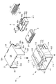
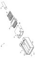
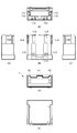
図15は、従来技術によるシールドコネクタの構成を示す斜視分解組立図である。図16は、従来技術によるシールドコネクタの部分構成を示す斜視分解組立図である。図17は、従来技術によるシールドコネクタの構成を示す斜視図であり、シールドコネクタをプリント基板に実装する前の状態図である。図18は、従来技術によるシールドコネクタの構成を示す図であり、図18(A)は、シールドコネクタの右側面図、図18(B)は、図18(A)の縦断面図である。 FIG. 15 is an exploded perspective view showing the configuration of a shield connector according to the prior art. FIG. 16 is an exploded perspective view showing a partial configuration of a shield connector according to the prior art. FIG. 17 is a perspective view showing the configuration of a shield connector according to the prior art, and is a state diagram before the shield connector is mounted on a printed circuit board. FIG. 18 is a view showing a configuration of a shield connector according to the prior art, FIG. 18 (A) is a right side view of the shield connector, and FIG. 18 (B) is a longitudinal sectional view of FIG.
なお、本願の図15と図16は、特許文献1の図2と図3に相当している。又、本願の図17と図18は、特許文献1の図8と図10に相当している。
FIGS. 15 and 16 of the present application correspond to FIGS. 2 and 3 of
図15から図18を参照すると、従来技術によるシールドコネクタ(以下、コネクタと略称する)9は、直方体状の外部ハウジング91と直方体状の内部ハウジング92を備えている。又、コネクタ9は、外部シェル93と内部シェル94を備えている。更に、コネクタ9は、複数の板状の第1コンタクト95と複数の板状の第2コンタクト96を備えている。
Referring to FIGS. 15 to 18, a shield connector (hereinafter referred to as a connector) 9 according to the prior art includes a rectangular parallelepiped
図15又は図17を参照すると、外部ハウジング91は、前面側に矩形に開口した収容室911を内部に有している。収容室911は、外部ハウジング91の後方側にも開口している。収容室911には、相手側コネクタ(図示せず)を前面側から挿入できる。又、収容室911には、内部シェル94で覆われた内部ハウジング92を外部ハウジング91の後方側から収容できる(図15参照)。
Referring to FIG. 15 or FIG. 17, the
図15又は図17を参照すると、外部シェル93は、外部ハウジング91の前面及び底面を除く四面を覆うことができる。同様に、内部シェル94は、内部ハウジング92の前面及び底面を除く四面を覆うことができる。
Referring to FIG. 15 or FIG. 17, the
図15を参照すると、外部ハウジング91は、一対のランス91r・91rを収容室911の内側壁に備えている。一対のランス91r・91rは、収容室911の後部側に配置されている。又、外部ハウジング91は、一組のランス91s・91sを収容室911の内上壁に備えている。一組のランス91s・91sは、収容室911の後部側に配置されている。
Referring to FIG. 15, the
一方、図15又は図16を参照すると、内部シェル94は、一対の帯板状の支持脚94f・94fと一対の矩形の開口94h・94hを有している。一対の支持脚94f・94fは、内部シェル94の底部側に突出している。一対の開口94h・94hは、天板941と背面板942に跨って開口している。図15に示すように、天板941に対して、背面板942を略直角に屈曲させた状態では、一対の開口94h・94hを介して、内部ハウジング92の角部を露出できる。
On the other hand, referring to FIG. 15 or FIG. 16, the
図15を参照して、内部シェル94付き内部ハウジング92を外部ハウジング91の後方側から挿入すると、一対のランス91r・91rの爪部を一対の支持脚94f・94fの端縁に係止できる。又、内部シェル94付き内部ハウジング92を外部ハウジング91の後方側から挿入すると、一対の開口94h・94hを介して、一組のランス91s・91sの爪部を内部ハウジング92の角部に係止できる。
Referring to FIG. 15, when the
図18(B)を参照すると、内部ハウジング92は、板状のヘッダ92hを一端側に突出している。ヘッダ92hは、相手側コネクタ(図示せず)に配置したヘッダが挿入自在な収容室921を内部に有している。収容室921の内上壁には、第1コンタクト95の接触部95cを配列している。又、収容室921の内下壁には、第2コンタクト96の接触部96cを配列している。
Referring to FIG. 18B, the
図18(B)を参照して、相手側コネクタ(図示せず)のヘッダを収容室921に挿入すると、相手側コンタクトと第1コンタクト95及び第2コンタクト96を電気的に接続できる。
Referring to FIG. 18B, when the header of the mating connector (not shown) is inserted into
図16を参照すると、第1コンタクト95は、リード部95rを他片に有している。同様に、第2コンタクト96は、リード部96rを他片に有している。一方、図17を参照すると、プリント基板9pには、これらのリード部95r及びリード部96rをハンダ接合自在な複数のスルーホール90sを開口している。これらのリード部95r及びリード部96rをスルーホール90sにハンダ接合することで、第1コンタクト95及び第2コンタクト96とプリント基板9pを電気的に接続できる。
Referring to FIG. 16, the
図15又は図16及び図18を参照すると、コネクタ9は、直方体状のスペーサ97を備えている。スペーサ97は、絶縁性を有する合成樹脂を成形している。スペーサ97は、第1コンタクト95の他片を保持している(図18参照)。又、スペーサ97は、第2コンタクト96の他片を保持している(図18参照)。
Referring to FIG. 15 or FIG. 16 and FIG. 18, the
図18を参照すると、スペーサ97は、第1コンタクト95の他片と第2コンタクト96の他片が所定に間隔を維持するように、第1コンタクト95と第2コンタクト96を保持している。又、図16又は図18を参照すると、スペーサ97は、隔壁97wを設けて、第1コンタクト95と内部シェル94の背面板942を隔絶している。
Referring to FIG. 18, the
図15又は図16及び図18を参照すると、外部シェル93は、矩形のタブ片93tを開口側に備えている。タブ片93tは、外部シェル93の天板931から起立している。タブ片93tは、エンボス93bを中央部に有している。エンボス93bには、雌ねじ部を形成している。
Referring to FIGS. 15 or 16 and 18, the
図18を参照して、図示しないパネルに開口した取り付け穴を介して、固定ねじをエンボス93bの雌ねじ部に締結することで、コネクタ9をパネルに固定できる。すなわち、コネクタ9を電子機器に実装できる。
Referring to FIG. 18,
図15から図18を参照すると、従来技術によるコネクタ9は、多数のコンタクトの周囲を二重に電磁遮蔽したシールドコネクタを実現している。
With reference to FIGS. 15-18, the
しかし、図18(B)を参照すると、従来技術によるコネクタ9は、第1コンタクト95と第2コンタクト96の間にスペーサ97を配置したこと、及び、外部シェル93の背面板932と内部シェル94の背面板942の間に空間を設けたことで、コネクタ9の奥行方向の長さを大きくしている、という問題がある。
However, referring to FIG. 18 (B), the
又、図15を参照すると、従来技術によるコネクタ9は、一対のランス91r・91rを収容室911の内部に配置しているので、コネクタ9の幅方向の長さを大きくしている、という問題がある。シールドコネクタの外形を小さくすることで、プリント基板の占有面積を縮小でき、プリント基板の過密実装と電子機器の小型化を期待できる。そして、以上のことが本発明の課題といってよい。
Further, referring to FIG. 15, the
本発明は、このような課題に鑑みてなされたものであり、多数のコンタクトの周囲を二重に電磁遮蔽したシールドコネクタであって、より小型化したシールドコネクタを提供することを目的とする。 The present invention has been made in view of such problems, and it is an object of the present invention to provide a shielded connector which is a shielded connector in which the periphery of a large number of contacts is doubly shielded electromagnetically and which is smaller in size.
本発明者らは、外部ハウジングと内部ハウジング、及び、外部シェルと内部シェルでシールドコネクタを構成し、外部シェルの背面板が近接自在に、複数のコンタクトを内部ハウジングの背面に同列に配置すると共に、内部シェルの両側面に配置した一対の圧入片が外部ハウジングの両側面に形成した圧入溝に係止自在に構成することで、小型化したシールドコネクタを実現できると考え、これに基づいて、以下のような新たなシールドコネクタを発明するに至った。 The present inventors constitute a shield connector with the outer housing and the inner housing, and the outer shell and the inner shell, and the back plate of the outer shell is closely accessible, and the plurality of contacts are arranged in the same row on the back of the inner housing. According to the invention, it is possible to realize a miniaturized shield connector by configuring a pair of press-fit pieces disposed on both sides of the inner shell to be freely lockable in press-fit grooves formed on both sides of the outer housing. We arrived at the invention of the following new shield connector.
(1)本発明によるシールドコネクタは、相手側のコネクタを挿入自在な矩形の開口を一方の面に有する収容室を内部に有する直方体状の外部ハウジングと、前記外部ハウジングの一方の面と底面を除く、当該外部ハウジングの外面を電磁遮蔽自在に覆う箱状の外部シェルと、前記外部ハウジングの一方の面と反対側の他方の面から前記収容室に収容し、当該収容室の内部の一部を電磁遮蔽自在に囲った角筒状の内部シェルと、一方の面に矩形の開口を有するコンタクト収容室を内部に有し、一方の面と反対側の他方の面を除く外面を前記内部シェルで覆った直方体状の内部ハウジングと、前記コンタクト収容室の内壁に一片を配列し、他片を前記内部ハウジングの他方に面に同列に配置し、一片に対して他片を略直角に屈曲した複数の板状の第1コンタクト及び第2コンタクトと、を備え、前記内部シェルは、他方の面から一方の面に向かって突出した一対の第1圧入片を両側部に有し、前記外部ハウジングは、一対の前記第1圧入片が圧入自在な圧入穴を他方の面の両側部に開口している。 (1) A shielded connector according to the present invention comprises a rectangular parallelepiped outer housing having a storage chamber having a rectangular opening on one side which has a rectangular opening into which a mating connector can be inserted, and one side and bottom of the outer housing A box-like outer shell which covers the outer surface of the outer housing in an electromagnetic shielding manner, and the other surface opposite to one surface of the outer housing is accommodated in the storage chamber, and a part of the inside of the storage chamber And a contact accommodating chamber having a rectangular opening on one surface, and the outer surface excluding the other surface opposite to the one surface is the inner shell. And one piece is arranged on the inner wall of the contact storage chamber, the other piece is arranged in the same row on the other side of the inner housing, and the other piece is bent substantially at a right angle to the one piece. Multiple plate shapes A first contact and a second contact, the inner shell having on both sides a pair of first press-in pieces projecting from the other surface toward the one surface, and the outer housing comprises the pair of the first and second contacts; The first press-fit piece is press-fit in a press-fit hole which is open on both sides of the other surface.
(2)前記内部シェルは、他方の面から起立すると共に、一方の面に向かって延出した一対の帯板状の第2圧入片を更に有し、前記外部ハウジングは、上面に穿設し、一対の前記第2圧入片を他方の面から導入自在な方形の圧入溝を有し、前記第2圧入片は、前記圧入溝の側面に係止自在な一つ以上のバーブを板厚面に有していることが好ましい。 (2) The inner shell further includes a pair of band plate-like second press-fit pieces extending toward the one surface while standing up from the other surface, and the outer housing is formed on the upper surface And a rectangular press-in groove capable of introducing the pair of second press-in pieces from the other side, and the second press-in piece is a thick plate surface of one or more barbs that can be locked on the side face of the press-in groove. It is preferable to have it.
(3)前記第2圧入片は、当該第2圧入片に片持ち支持し、上り傾斜した状態で配置され、先端部が前記外部シェルの天板の内壁に接触自在なばね片を有していることが好ましい。 (3) The second press-in piece is cantilevered on the second press-in piece and disposed in an inclined state, and the tip portion has a spring piece that can contact the inner wall of the top plate of the outer shell Is preferred.
(4)前記外部ハウジングは、前記収容室に連通する一対の窓を両側面に有し、前記外部シェルは、その両側面から段差を有して内部側に沈下し、前記窓を封鎖する一対の凹部片を有し、前記凹部片は、前記外部シェルの底部に向かって突出し、プリント基板にハンダ接合自在な支持脚を有し、前記支持脚は、前記外部ハウジングに係止自在な一つ以上のバーブを板厚面に有していることが好ましい。 (4) The outer housing has a pair of windows communicating with the storage chamber on both sides, and the outer shell has a step from the both sides and sinks to the inside, thereby closing the windows And a support leg projecting toward the bottom of the outer shell and having a support leg solderable to a printed circuit board, the support leg being a lockable one on the outer housing It is preferable to have the above-described barbs on the thick surface.
(5)前記第1コンタクト及び第2コンタクトは、プリント基板の表面にハンダ接合なリード部を他片に有していることが好ましい。 (5) It is preferable that the first contact and the second contact have a lead portion soldered to the surface of the printed circuit board on the other side.
本発明によるシールドコネクタは、外部ハウジングと内部ハウジング、及び、外部シェルと内部シェルを備え、外部シェルの背面板が近接自在に、複数のコンタクトを内部ハウジングの背面に同列に配置すると共に、内部シェルの両側面に配置した一対の圧入片が外部ハウジングの両側面に形成した圧入溝に係止自在に構成することで、従来技術によるスペーサ及び一対の内部ランスを不要とし、シールドコネクタをより小型化できる。 The shield connector according to the present invention comprises an outer housing and an inner housing, and an outer shell and an inner shell, wherein the back plate of the outer shell is closely accessible, and the plurality of contacts are arranged in the same row on the back of the inner housing. A pair of press-fit pieces arranged on both sides of the housing can be freely locked in press-fit grooves formed on both sides of the outer housing, thereby eliminating the need for the spacer and the pair of internal lances according to the prior art and further downsizing the shield connector. it can.
以下、図面を参照して本発明を実施するための形態を説明する。 Hereinafter, embodiments of the present invention will be described with reference to the drawings.
[シールドコネクタの構成]
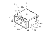
最初に、本発明の一実施形態によるシールドコネクタの構成を説明する。図1は、本発明の一実施形態によるシールドコネクタの構成を示す斜視図であり、プリント基板に実装したシールドコネクタに対して、相手側のコネクタを対向配置した状態図である。
[Configuration of shield connector]
First, the configuration of a shielded connector according to an embodiment of the present invention will be described. FIG. 1 is a perspective view showing the configuration of a shielded connector according to an embodiment of the present invention, and is a state diagram in which a mating connector is disposed opposite to a shielded connector mounted on a printed circuit board.
図2は、前記実施形態によるシールドコネクタの構成を示す斜視図である。図3は、前記実施形態によるシールドコネクタに接続自在な相手側のコネクタの構成を示す斜視図である。 FIG. 2 is a perspective view showing the configuration of the shield connector according to the embodiment. FIG. 3 is a perspective view showing the configuration of a mating connector which can be connected to the shield connector according to the embodiment.
図4は、前記実施形態によるシールドコネクタの構成を示す斜視分解組立図である。図5は、相手側のコネクタの構成を示す斜視分解組立図である。 FIG. 4 is an exploded perspective view showing the configuration of the shield connector according to the embodiment. FIG. 5 is a perspective exploded view showing the configuration of the mating connector.
図6は、前記実施形態によるシールドコネクタの構成を示す斜視分解組立図であり、シールドコネクタの各構成品を背面側から観た状態図である。 FIG. 6 is an exploded perspective view showing the configuration of the shield connector according to the embodiment, and is a state diagram when each component of the shield connector is viewed from the back side.
図7は、前記実施形態によるシールドコネクタに備わる外部ハウジングの構成を示す図であり、図7(A)は、外部ハウジングの正面図、図7(B)は、外部ハウジングの平面図、図7(C)は、外部ハウジングの右側面図、図7(D)は、外部ハウジングの左側面図、図7(E)は、外部ハウジングの背面図、図7(F)は、外部ハウジングの下面図である。 FIG. 7 is a view showing the structure of the outer housing provided in the shield connector according to the embodiment, FIG. 7 (A) is a front view of the outer housing, FIG. 7 (B) is a plan view of the outer housing, FIG. (C) is a right side view of the outer housing, FIG. 7 (D) is a left side view of the outer housing, FIG. 7 (E) is a rear view of the outer housing, and FIG. FIG.
図8は、前記実施形態によるシールドコネクタに備わる外部シェルの構成を示す図であり、図8(A)は、外部シェルの正面図、図8(B)は、外部シェルの平面図、図8(C)は、外部シェルの右側面図、図8(D)は、外部シェルの左側面図、図8(E)は、外部シェルの背面図、図8(F)は、外部シェルの下面図である。 FIG. 8 is a view showing a configuration of an outer shell provided in the shield connector according to the embodiment, FIG. 8 (A) is a front view of the outer shell, FIG. 8 (B) is a plan view of the outer shell, (C) is a right side view of the outer shell, FIG. 8 (D) is a left side view of the outer shell, FIG. 8 (E) is a rear view of the outer shell, and FIG. 8 (F) is a lower surface of the outer shell FIG.
図9は、前記実施形態によるシールドコネクタの縦断面を示す斜視図である。図10は、前記実施形態によるシールドコネクタの構成を示す斜視図であり、外部シェルを取り外したシールドコネクタを背面側から観た状態図である。 FIG. 9 is a perspective view showing a longitudinal cross section of the shielded connector according to the embodiment. FIG. 10 is a perspective view showing the configuration of the shield connector according to the embodiment, and is a state view of the shield connector from which the outer shell has been removed, viewed from the back side.
図11は、図10の要部を拡大した斜視図である。図12は、図10の要部を拡大した斜視図である。図13は、図9の要部を拡大した縦断面斜視図である。図14は、前記実施形態によるシールドコネクタに備わる第1コンタクト及び第2コンタクトの構成を示す斜視図である。 FIG. 11 is an enlarged perspective view of the main part of FIG. FIG. 12 is an enlarged perspective view of the main part of FIG. FIG. 13 is a vertical cross-sectional perspective view in which the main part of FIG. 9 is enlarged. FIG. 14 is a perspective view showing the configuration of the first contact and the second contact provided in the shielded connector according to the embodiment.
(全体構成)
図1から図13を参照すると、本発明の一実施形態によるシールドコネクタ(以下、リセプタクルという)10は、直方体状の外部ハウジング1と箱状の外部シェル3を備えている。外部ハウジング1は、収容室11を内部に有している。収容室11は、矩形の開口11aを前面側(一方の面)に有している。収容室11には、その前面側から相手側のコネクタ(以下、プラグという)20を挿入できる(図1参照)。
(overall structure)
With reference to FIGS. 1 to 13, a shield connector (hereinafter referred to as a receptacle) 10 according to an embodiment of the present invention includes a rectangular parallelepiped
図1又は図2及び図4又は図6を参照すると、外部シェル3は、天板31、一対の側面板32・32、及び、背面板33で構成している。外部シェル3は、外部ハウジング1の前面と底面を除く、外部ハウジング1の外面を電磁遮蔽自在に覆うことができる。
Referring to FIG. 1 or FIG. 2 and FIG. 4 or FIG. 6, the
又、図1から図14を参照すると、リセプタクル10は、角筒状の内部シェル4、直方体状の内部ハウジング5、及び、複数の板状の第1コンタクト61及び第2コンタクト62を備えている。
Further, referring to FIGS. 1 to 14, the
図4又は図6を参照すると、内部シェル4は、外部ハウジング1の背面(他方の面)側から収容室11に収容できる。そして、内部シェル4は、収容室11の内部を電磁遮蔽自在に囲っている(図9参照)。
With reference to FIG. 4 or FIG. 6, the
図4又は図6及び図9を参照すると、内部ハウジング5は、コンタクト収容室51を内部に有している。コンタクト収容室51は、矩形の開口を前面に有している。又、内部ハウジング5は、前面と反対側の背面を除く外面を内部シェル4で覆っている。
Referring to FIG. 4 or FIG. 6 and FIG. 9, the
図9又は図10及び図14を参照すると、第1コンタクト61は、一片611に対して他片612を略直角に屈曲している(図14参照)。同様に、第2コンタクト62は、一片621に対して他片622を略直角に屈曲している(図14参照)。
Referring to FIGS. 9 or 10 and 14, the
図9を参照すると、第1コンタクト61の一片611は、コンタクト収容室51の上内壁に配列している。一方、第2コンタクト62の一片621は、コンタクト収容室51の底壁に配列している。そして、第1コンタクト61の他片612及び第2コンタクト62の他片622は、内部ハウジング5の背面に同列に配置している(図10参照)。
Referring to FIG. 9, one
図4又は図6及び図10又は図12を参照すると、内部シェル4は、一対一組の第1圧入片41p・41pを背面側の両側部に有している。これらの第1圧入片41p・41pは、内部シェル4の背面から前面に向かって突出している。
Referring to FIG. 4 or FIG. 6 and FIG. 10 or FIG. 12, the
一方、図6又は図7を参照すると、外部ハウジング1は、一対一組の圧入穴11h・11hを背面の両側部に開口している。これらの圧入穴11h・11hには、一対一組の第1圧入片41p・41pを圧入できる(図10又は図12参照)。そして、内部ハウジング5を保持した内部シェル4を外部ハウジング1に固定できる(図10参照)。
On the other hand, referring to FIG. 6 or 7, the
図9又は図10を参照すると、リセプタクル10は、外部シェル3の背面板33を第1コンタクト61の他片612及び第2コンタクト62の他片622に近接配置している。
9 or 10, the
又、図9又は図10を参照すると、リセプタクル10は、第1コンタクト61の他片612及び第2コンタクト62の他片622を内部ハウジング5の背面に同列に配置している。これにより、第1コンタクトの他片と第2コンタクトの他片が所定に間隔を維持するためのスペーサ97を不要とし(図18(B)参照)、リセプタクル10の奥行方向の長さを小さくできる。
9 or 10, the
図4又は図6及び図10又は図12を参照すると、リセプタクル10は、内部シェル4に形成した一対一組の第1圧入片41p・41pを外部ハウジング1の背面に開口した圧入穴11h・11hに圧入することで、内部シェル4を外部ハウジング1に固定している。これにより、従来技術による一対のランス91r・91rを不要とし(図15参照)、リセプタクル10の幅方向の長さを小さくできる。
With reference to FIG. 4 or FIG. 6 and FIG. 10 or FIG. 12, the
(相手側のコネクタの構成)
次に、実施形態によるリセプタクル10の各構成品を説明する前に、相手側のコネクタであるプラグ20の構成を説明する。なお、相手側のコネクタは、図示したプラグ20に限定されない。
(Configuration of the other party's connector)
Next, before describing the components of the
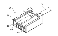
図1又は図3及び図5を参照すると、プラグ20は、ケーブルCbの端末に取り付けられている。プラグ20は、直方体状の外部ハウジング21と角筒状のシェル22を備えている。又、プラグ20は、直方体状の内部ハウジング23と複数のベローズ形のコンタクト24を備えている。
Referring to FIGS. 1 or 3 and 5, the
図1又は図3及び図5を参照すると、外部ハウジング21は、その大部分を外部ハウジング1の収容室11に挿入できる。外部ハウジング21は、中央キー211と一対の側部キー212・212を上面から隆起している。中央キー211と一対の側部キー212・212を外部ハウジング21の上面に形成することで、リセプタクル10に対するプラグ20の誤挿入を防止できる。
Referring to FIGS. 1 or 3 and 5, most of the
図1又は図3及び図5を参照すると、中央キー211は、その末端部側が操作自在な押動レバーになっている。中央キー211は、三角形体状のランス21rを末端部側から突出している。
Referring to FIG. 1 or FIG. 3 and FIG. 5, the
図1を参照して、プラグ20をリセプタクル10に挿入すると、外部ハウジング1の前面側に開口した係止穴111にランス21rを係止できる。つまり、プラグ20をリセプタクル10にロックできる。一方、中央キー211の末端部を押動操作すると、係止穴111からランス21rを解除でき、プラグ20をリセプタクル10から引き抜くことができる。
Referring to FIG. 1, when the
図3又は図5を参照すると、外部ハウジング21は、収容室213を内部に有している。収容室213は、矩形の開口を前面側に有している。図1を参照して、プラグ20をリセプタクル10に挿入すると、内部ハウジング5付き内部シェル4(図9参照)を収容室213に収容できる。
Referring to FIG. 3 or 5, the
図3又は図5を参照すると、シェル22は、外部ハウジング21の前面側から収容室213に収容できる。そして、シェル22は、収容室213の内部を電磁遮蔽自在に囲っている。
With reference to FIG. 3 or FIG. 5, the
図3又は図5を参照すると、内部ハウジング23は、シェル22の背面側から内部に挿入できる。そして、内部ハウジング23は、シェル22で電磁遮蔽自在に覆われている。内部ハウジング23は、板状のヘッダ23hを一端部側に突出している(図5参照)。ヘッダ23hは、コンタクト収容室51に嵌合できる(図9参照)。
Referring to FIG. 3 or FIG. 5, the
図5を参照すると、ヘッダ23hには、複数のコンタクト24の自由端部を配列している。複数のコンタクト24は、それらの自由端部の屈曲部が相反する向きに向かうように、ヘッダ23hに配列されている。ヘッダ23hをコンタクト収容室51に挿入すると(図9参照)、プラグ20に配列した複数のコンタクト24を第1コンタクト61の一片611及び第2コンタクト62の一片621に接触できる。
Referring to FIG. 5, in the
図5を参照すると、ケーブルCbは、その内部に複数の電線(図示せず)を収容している。複数のコンタクト24の固定端部は、前記電線の端末と結線している。そして、図1を参照して、プラグ20をリセプタクル10に挿入すると、ケーブルCbとリセプタクル10を電気的に接続できる。又、ケーブルCbとプリント基板9pを電気的に接続できる、ということもできる(図1参照)。
Referring to FIG. 5, the cable Cb accommodates therein a plurality of electric wires (not shown). The fixed ends of the plurality of
(外部ハウジングの構成)
次に、実施形態による外部ハウジング1の構成を説明する。図4又は図6及び図7を参照すると、外部ハウジング1は、絶縁性を有している。非導電性の材料からなる合成樹脂を成形して、所望の形状の絶縁性の外部ハウジング1を得ることができる。
(Configuration of external housing)
Next, the configuration of the
図1又は図2及び図4を参照すると、外部ハウジング1は、開口11aの上部の中央部にキー溝k1を切り欠いている。又、外部ハウジング1は、キー溝k1の両側に一対のキー溝k2・k2を切り欠いている。これらのキー溝k1及び一対のキー溝k2・k2は、中央キー211と一対の側部キー212・212に嵌合できる。そして、リセプタクル10に対するプラグ20の誤挿入を防止できる。
With reference to FIG. 1 or FIG. 2 and FIG. 4, the
図1又は図2及び図4を参照すると、外部ハウジング1は、その前面側に係止穴111を開口している。係止穴111は、キー溝k1に連通している。図1を参照して、プラグ20をリセプタクル10に挿入すると、キー溝k1を介して、ランス21rを係止穴111に係止できる。
Referring to FIG. 1 or FIG. 2 and FIG. 4, the
図4又は図6及び図7(B)を参照すると、外部ハウジング1は、その前面側の上面に一対の係止穴112・112を開口している。一方、図4又は図8(A)を参照すると、外部シェル3は、天板31の端部から一対の爪片311・311を突出している。図4を参照して、外部シェル3を外部ハウジング1に向かって挿入すると、爪片311を係止穴112に係止できる。そして、外部シェル3を外部ハウジング1に固定できる(図1又は図2参照)。
Referring to FIG. 4 or FIG. 6 and FIG. 7 (B), the
図4又は図6及び図7(B)を参照すると、外部ハウジング1は、その背面側の上面に一対の方形の圧入溝113・113を穿設している。一方、図4又は図6を参照すると、内部シェル4は、一対の帯板状の第2圧入片42p・42pを有している。
Referring to FIG. 4 or FIG. 6 and FIG. 7 (B), the
図4又は図6を参照すると、一対の第2圧入片42p・42pは、内部シェル4の背面から起立すると共に、前面に向かって延出している。図4又は図6及び図7(B)を参照すると、一対の圧入溝113・113には、外部ハウジング1の背面側から第2圧入片42p・42pを導入できる。
Referring to FIG. 4 or 6, the pair of second press-
図11を参照すると、第2圧入片42pは、その板厚面から突出する一対のバーブ(barb:刺)42b・42bを有している。外部ハウジング1の背面側から第2圧入片42pを圧入溝113に導入すると、一対のバーブ42b・42bを圧入溝113の側面に係止できる。つまり、外部シェル3を外部ハウジング1に固定できる(図13参照)。
Referring to FIG. 11, the second press-
図4又は図6及び図7を参照すると、外部ハウジング1は、一対の窓11w・11wを両側面に開口している。一対の窓11w・11wは、収容室11に連通している。
Referring to FIGS. 4 or 6 and 7, the
一方、図4又は図6及び図8を参照すると、外部シェル3は、一対の窓11w・11wを封鎖する一対の凹部片32c・32cを有している。凹部片32cは、側面板32から段差を有して内部側に沈下している。なお、窓11wと凹部片32cとの関係は、後述する。
On the other hand, referring to FIG. 4 or FIG. 6 and FIG. 8, the
(外部シェルの構成)
次に、実施形態による外部シェル3の構成を説明する。図4又は図6及び図8を参照すると、外部シェル3は、導電性を有する展開板を成形して箱状に構成している。外部シェル3は、前面及び底面を開放している。
(Configuration of external shell)
Next, the configuration of the
図4又は図6及び図8には図示していないが、外部シェル3は、天板31から連続して背面側に延びる背面板33を有している。天板31に対して、背面板33を略直角に折り曲げることで、外部ハウジング1の背面側を電磁遮蔽(シールド)できる(図9参照)。
Although not shown in FIG. 4 or FIG. 6 and FIG. 8, the
図4又は図6及び図8を参照すると、凹部片32cは、支持脚321を有している。支持脚321は、プリント基板9pにハンダ接合できる(図1参照)。又、側面板32は、支持脚322を前面側から突出している。支持脚322は、プリント基板9pにハンダ接合できる(図1参照)。つまり、実施形態によるリセプタクル10は、プリント基板9pに実装自在なプリント基板用コネクタである。
Referring to FIGS. 4 or 6 and 8, the
図7(B)を参照すると、外部ハウジング1は、一対の係止穴114・114を背面側に開口している。係止穴114は、窓11wに連通している。図4又は図8を参照すると、支持脚321は、その板厚面から突出する一対のバーブ32b・32bを基端部側に有している。支持脚321を係止穴114に挿入すると、これらのバーブ32b・32bを係止穴114の内壁に係止できる。つまり、外部シェル3を外部ハウジング1に固定できる(図1又は図2参照)。
Referring to FIG. 7 (B), the
(内部シェルの構成)
次に、実施形態による内部シェル4の構成を説明する。図4又は図6を参照すると、内部シェル4は、導電性を有する帯状の展開板を成形して矩形の角筒状に構成している。内部シェル4の形状を保全するために、前記展開板は、下面板の中央部で互いに噛み合う凹凸状のシーム(継ぎ目)42j(図4参照)を両端縁部に形成している。そして、前記展開板を角筒状に成形し、この展開板の両端縁を繋ぎ合わせることで、上面板、一対の側面板、及び、下面板で囲われた矩形の開口を得ることができる。
(Configuration of inner shell)
Next, the configuration of the
図4又は図10及び図11を参照すると、第2圧入片42pは、ばね片42sを有している。ばね片42sは、第2圧入片42pに片持ち支持されている。ばね片42sは、第2圧入片42pから上り傾斜した状態で配置されている。
Referring to FIG. 4 or FIG. 10 and FIG. 11, the second press-
図4を参照して、外部シェル3を外部ハウジング1に向かって挿入すると、ばね片42sの先端部を外部シェル3の天板31の内壁に接触できる(図13参照)。これにより、外部シェル3と内部シェル4を確実に導通でき、シールド効果を向上できる。
Referring to FIG. 4, when the
図4又は図6及び図10を参照すると、内部シェル4は、一対の脚片411・411を有している。脚片411の基端部には、第1圧入片41pを配置している。図10を参照して、一対一組の第1圧入片41p・41pを外部ハウジング1の背面側に圧入した状態では、一対の脚片411・411は、その先端部が外部ハウジング1の底面から突出している。
Referring to FIG. 4 or 6 and 10, the
図1又は図10を参照して、一対の脚片411・411は、その先端部をプリント基板9pに開口したスルーホール(図示せず)にハンダ接合できる。すなわち、実施形態によるリセプタクル10は、プリント基板9pの表面に実装自在なプリント基板用コネクタである。
With reference to FIG. 1 or 10, the pair of
(内部ハウジングの構成)
次に、実施形態による内部ハウジング5の構成を説明する。図4又は図6及び図9を参照すると、内部ハウジング5は、絶縁性を有している。非導電性の材料からなる合成樹脂を成形して、所望の形状の絶縁性の内部ハウジング5を得ることができる。
(Configuration of inner housing)
Next, the configuration of the
図4又は図6及び図9を参照すると、内部ハウジング5は、内部シェル4を介して、外部ハウジング1の背面側に支持されている。図1から図3及び図9を参照して、プラグ20を外部ハウジング1の収容室11に挿入した状態では、プラグ20のシェル22とリセプタクル10の内部シェル4を導通自在に嵌合している。
Referring to FIGS. 4 or 6 and 9, the
又、図1から図3及び図9を参照して、プラグ20を外部ハウジング1の収容室11に挿入した状態では、プラグ20のヘッダ23hを内部ハウジング5のコンタクト収容室51に挿入している。そして、プラグ20に配列した複数のコンタクト24を第1コンタクト61の一片611及び第2コンタクト62の一片621に接触できる。
Further, referring to FIGS. 1 to 3 and 9, in the state in which plug 20 is inserted into
(コンタクトの構成)
次に、実施形態による第1コンタクト61及び第2コンタクト62の構成を説明する。図4又は図6及び図14を参照して、第1コンタクト61及び第2コンタクト62は、導電性を有している。導電性の金属板を打ち抜き加工又は折り曲げ加工して、所望の形状の導電性の第1コンタクト61及び第2コンタクト62を得ることができる。
(Configuration of contacts)
Next, configurations of the
図4又は図6及び図14を参照して、第1コンタクト61及び第2コンタクト62は、加工の容易性や、ばね特性、導電性などを考慮すれば、例えば、銅合金が好ましく用いられるが、銅合金に限定される訳ではない。
With reference to FIG. 4 or FIG. 6 and FIG. 14, for the
図14を参照すると、第1コンタクト61の一片611は、複数のバーブを板厚面からに突出している。一方、図13を参照すると、内部ハウジング5は、複数の浅溝51dをコンタクト収容室51の上内壁に穿設している。第1コンタクト61の一片611をコンタクト収容室51の浅溝51dに圧入することで、第1コンタクト61を内部ハウジング5に固定できる。
Referring to FIG. 14, a
同様に、図14を参照すると、第2コンタクト62の一片621は、複数のバーブを板厚面からに突出している。一方、図13を参照すると、内部ハウジング5は、複数の浅溝52dをコンタクト収容室51の底内壁に穿設している。第2コンタクト62の一片621をコンタクト収容室51の浅溝52dに圧入することで、第1コンタクト61を内部ハウジング5に固定できる。
Similarly, referring to FIG. 14, a
図14を参照すると、第1コンタクト61の他片612は、リード部61rを先端部に有している。リード部61rは、一片611と反対側に延出している。同様に、第2コンタクト62の他片622は、リード部62rを先端部に有している。リード部62rは、一片621と反対側に延出している。これらのリード部61r・62rは、プリント基板9pの表面に形成したパターン(図示せず)にハンダ接合できる(図1参照)。すなわち、実施形態によるリセプタクル10は、プリント基板9pの表面にハンダ接合が自在な表面実装用コネクタである(図1参照)。
Referring to FIG. 14, the
[シールドコネクタの作用]
次に、実施形態によるリセプタクル10の作用及び効果を説明する。図1から図14を参照すると、リセプタクル10は、第1コンタクト61の他片612及び第2コンタクト62の他片622を内部ハウジング5の背面に同列に配置している(図9又は図10参照)。これにより、第1コンタクトの他片と第2コンタクトの他片が所定に間隔を維持するためのスペーサ97を不要にできる(図18(B)参照)。そして、リセプタクル10の奥行方向の長さを小さくできる。
[Function of shield connector]
Next, the operation and effects of the
又、図1から図14を参照すると、リセプタクル10は、内部シェル4に形成した一対一組の第1圧入片41p・41pを外部ハウジング1の背面に開口した圧入穴11h・11hに圧入することで、内部シェル4を外部ハウジング1に固定している。これにより、従来技術による一対のランス91r・91rを不要とし(図15参照)、リセプタクル10の幅方向の長さを小さくできる。
Further, referring to FIGS. 1 to 14, the
図1から図14を参照すると、実施形態によるリセプタクル10は、外部ハウジング1と内部ハウジング5、及び、外部シェル3と内部シェル4を備え、外部シェル3の背面板33が近接自在に、複数の第1コンタクト61及び第2コンタクト62を内部ハウジング5の背面に同列に配置すると共に、内部シェル4の両側面に配置した一対の第1圧入片41p・41pが外部ハウジング1の両側面に形成した圧入溝113・113に係止自在に構成することで、従来技術によるスペーサ及び一対の内部ランスを不要とし、シールドコネクタをより小型化できる。
1 to 14, the
又、図4又は図10及び図11を参照すると、実施形態によるリセプタクル10は、外部シェル3の天板31の内壁に接触自在な、一対のばね片42s・42sを内部シェル4の上部に備えているので、外部シェル3と内部シェル4を確実に導通でき、シールド効果を向上できる。
Also, referring to FIG. 4 or FIG. 10 and FIG. 11, the
本発明は、シールド性能を向上すると共に、小型化した車載用のHDMIコネクタ(リセプタクル)を開示したが、本発明によるシールドコネクタは、HDMIコネクタに限定されない。 Although the present invention has improved the shielding performance and disclosed a miniaturized in-vehicle HDMI connector (receptacle), the shielded connector according to the present invention is not limited to the HDMI connector.
1 外部ハウジング
3 外部シェル
4 内部シェル
5 内部ハウジング
10 リセプタクル(シールドコネクタ)
11 収容室
11a 開口
11h 圧入穴
20 プラグ(相手側のコネクタ)
33 背面板
41p・41p 一対の第1圧入片
51 コンタクト収容室
61 第1コンタクト
62 第2コンタクト
611 一片(第1コンタクトの一片)
612 他片(第1コンタクトの他片)
621 一片(第2コンタクトの一片)
622 他片(第2コンタクトの他片)
1
11
33
612 Other piece (other piece of first contact)
621 piece (one piece of second contact)
622 Another piece (the other piece of the second contact)
Claims (5)
前記外部ハウジングの一方の面と底面を除く、当該外部ハウジングの外面を電磁遮蔽自在に覆う箱状の外部シェルと、
前記外部ハウジングの一方の面と反対側の他方の面から前記収容室に収容し、当該収容室の内部の一部を電磁遮蔽自在に囲った角筒状の内部シェルと、
一方の面に矩形の開口を有するコンタクト収容室を内部に有し、一方の面と反対側の他方の面を除く外面を前記内部シェルで覆った直方体状の内部ハウジングと、
前記コンタクト収容室の内壁に一片を配列し、他片を前記内部ハウジングの他方に面に同列に配置し、一片に対して他片を略直角に屈曲した複数の板状の第1コンタクト及び第2コンタクトと、を備え、
前記内部シェルは、他方の面から一方の面に向かって突出した一対の第1圧入片を両側部に有し、
前記外部ハウジングは、一対の前記第1圧入片が圧入自在な圧入穴を他方の面の両側部に開口している、シールドコネクタ。 A rectangular parallelepiped outer housing internally having a storage chamber having a rectangular opening on one surface thereof into which a mating connector can be inserted;
A box-like outer shell that electromagnetically shields the outer surface of the outer housing excluding one side and the bottom of the outer housing;
A rectangular cylindrical inner shell which is accommodated in the accommodation chamber from the other surface opposite to the one surface of the outer housing, and a part of the interior of the accommodation chamber is electromagnetically shielded;
A rectangular solid inner housing having a contact storage chamber having a rectangular opening on one side and the outer surface covered by the inner shell except the other side opposite to the one side;
A plurality of plate-like first contacts in which one piece is arranged on the inner wall of the contact chamber, the other piece is arranged in the same row on the other side of the inner housing, and the other piece is bent substantially at right angles to the piece With 2 contacts,
The inner shell has on both sides a pair of first press-in pieces which project from the other side toward the one side,
The shield connector, wherein the outer housing has a press-fit hole through which a pair of the first press-fit pieces can be press-fit, on both sides of the other face.
前記外部ハウジングは、上面に穿設し、一対の前記第2圧入片を他方の面から導入自在な方形の圧入溝を有し、
前記第2圧入片は、前記圧入溝の側面に係止自在な一つ以上のバーブを板厚面に有している、請求項1記載のシールドコネクタ。 The inner shell further includes a pair of strip-shaped second press-in pieces which rise from the other surface and extend toward the one surface;
The outer housing has a rectangular press-in groove which is drilled on the upper surface and in which the pair of second press-in pieces can be introduced from the other side;
The shield connector according to claim 1, wherein the second press-fit piece has one or more barbs that can be locked to the side surface of the press-fit groove on a thick plate surface.
前記外部シェルは、その両側面から段差を有して内部側に沈下し、前記窓を封鎖する一対の凹部片を有し、
前記凹部片は、前記外部シェルの底部に向かって突出し、プリント基板にハンダ接合自在な支持脚を有し、
前記支持脚は、前記外部ハウジングに係止自在な一つ以上のバーブを板厚面に有している、請求項1から3のいずれかに記載のシールドコネクタ。 The outer housing has a pair of windows on both sides communicating with the storage chamber,
The outer shell has a pair of recessed pieces which are recessed inwardly with a step from both sides thereof and which closes the window;
The recess piece protrudes toward the bottom of the outer shell and has a support leg that can be soldered to a printed circuit board.
The shield connector according to any one of claims 1 to 3, wherein the support leg has one or more barbs that can be locked to the outer housing on a thick plate surface.
Priority Applications (2)
| Application Number | Priority Date | Filing Date | Title |
|---|---|---|---|
| JP2015230957A JP6534917B2 (en) | 2015-11-26 | 2015-11-26 | Shield connector |
| CN201611050803.3A CN107017527B (en) | 2015-11-26 | 2016-11-24 | Shielded connector |
Applications Claiming Priority (1)
| Application Number | Priority Date | Filing Date | Title |
|---|---|---|---|
| JP2015230957A JP6534917B2 (en) | 2015-11-26 | 2015-11-26 | Shield connector |
Publications (2)
| Publication Number | Publication Date |
|---|---|
| JP2017098154A JP2017098154A (en) | 2017-06-01 |
| JP6534917B2 true JP6534917B2 (en) | 2019-06-26 |
Family
ID=58805035
Family Applications (1)
| Application Number | Title | Priority Date | Filing Date |
|---|---|---|---|
| JP2015230957A Active JP6534917B2 (en) | 2015-11-26 | 2015-11-26 | Shield connector |
Country Status (2)
| Country | Link |
|---|---|
| JP (1) | JP6534917B2 (en) |
| CN (1) | CN107017527B (en) |
Families Citing this family (2)
| Publication number | Priority date | Publication date | Assignee | Title |
|---|---|---|---|---|
| KR102569847B1 (en) * | 2021-06-25 | 2023-08-23 | 주식회사 센서뷰 | Connector assembly including receptacle connector and plug connector, and plug connector |
| JP7634849B2 (en) * | 2022-03-24 | 2025-02-25 | トヨタ紡織株式会社 | Ultraviolet irradiation equipment |
Family Cites Families (12)
| Publication number | Priority date | Publication date | Assignee | Title |
|---|---|---|---|---|
| JP3423786B2 (en) * | 1994-10-04 | 2003-07-07 | Smk株式会社 | Double shielded connector |
| JP3229272B2 (en) * | 1998-10-21 | 2001-11-19 | ヒロセ電機株式会社 | Shield connector |
| US6379184B1 (en) * | 1999-07-16 | 2002-04-30 | Molex Incorporated | Connectors with reduced noise characteristics |
| JP5038818B2 (en) * | 2007-08-22 | 2012-10-03 | 株式会社オートネットワーク技術研究所 | Board connector |
| JP5660925B2 (en) * | 2010-04-07 | 2015-01-28 | 日本航空電子工業株式会社 | connector |
| JP3161645U (en) * | 2010-05-25 | 2010-08-05 | 正▲うえ▼精密工業股▲ふん▼有限公司 | Electrical connector |
| US8021188B1 (en) * | 2010-08-04 | 2011-09-20 | Cheng Uei Precision Industry Co., Ltd. | Electrical connector |
| JP5524009B2 (en) * | 2010-09-28 | 2014-06-18 | ホシデン株式会社 | Connectors and electronic devices |
| JP5836715B2 (en) * | 2011-09-07 | 2015-12-24 | 矢崎総業株式会社 | Shield connector |
| JP5725557B2 (en) * | 2011-10-21 | 2015-05-27 | 日本航空電子工業株式会社 | Connector and method for manufacturing outer shell of connector |
| JP2015176657A (en) * | 2014-03-13 | 2015-10-05 | ホシデン株式会社 | connector |
| JP6319657B2 (en) * | 2014-05-14 | 2018-05-09 | Smk株式会社 | Shield connector |
-
2015
- 2015-11-26 JP JP2015230957A patent/JP6534917B2/en active Active
-
2016
- 2016-11-24 CN CN201611050803.3A patent/CN107017527B/en active Active
Also Published As
| Publication number | Publication date |
|---|---|
| JP2017098154A (en) | 2017-06-01 |
| CN107017527B (en) | 2019-06-11 |
| CN107017527A (en) | 2017-08-04 |
Similar Documents
| Publication | Publication Date | Title |
|---|---|---|
| US10096947B2 (en) | Electrical connector and electrical device assembled with the same therein | |
| TWI758340B (en) | Receptacle connector | |
| US7108554B2 (en) | Electrical connector with shielding member | |
| US7128607B2 (en) | Socket connector with reliable shielding member | |
| US7766674B1 (en) | Electrical connector with high profile | |
| US6923687B2 (en) | Audio jack having improved contacts | |
| US10361518B2 (en) | Electrical connector having shielding plate retained tightly thereto | |
| US9780490B2 (en) | Cable connector having a metal shell with a metal cage at its rear end enclosed by an outer housing | |
| US9748712B2 (en) | Electrical connector having inserted insulator and method of making the same | |
| JP7606661B2 (en) | PCB Connectors and Devices | |
| US20090227138A1 (en) | Electrical connector adapter for connecting with two rows of cables | |
| JP7713162B2 (en) | PCB Connectors and Devices | |
| US9444161B2 (en) | Multiple-in-one receptacle connector | |
| JP2007180008A (en) | Connector plug | |
| WO2023008035A1 (en) | Substrate connnector and device | |
| US7311556B2 (en) | Electrical connector | |
| US9385487B2 (en) | Active plug connector and method for assembling the same | |
| US20150087165A1 (en) | Receptacle connector with double metallic shells | |
| US7112099B2 (en) | Audio jack connector | |
| JP6534917B2 (en) | Shield connector | |
| US6699071B1 (en) | Electrical connector with retention mechanism of outer shell | |
| US7241160B2 (en) | Shielded electrical connector for camera module | |
| KR101285675B1 (en) | Housing structure for electronic device, as well as method for creating such a housing structure | |
| US20150207269A1 (en) | Card connector with metallic retaining plate | |
| US9742119B2 (en) | Plug connector assembly with shielding shell |
Legal Events
| Date | Code | Title | Description |
|---|---|---|---|
| A621 | Written request for application examination |
Free format text: JAPANESE INTERMEDIATE CODE: A621 Effective date: 20180920 |
|
| A977 | Report on retrieval |
Free format text: JAPANESE INTERMEDIATE CODE: A971007 Effective date: 20190418 |
|
| TRDD | Decision of grant or rejection written | ||
| A01 | Written decision to grant a patent or to grant a registration (utility model) |
Free format text: JAPANESE INTERMEDIATE CODE: A01 Effective date: 20190507 |
|
| A61 | First payment of annual fees (during grant procedure) |
Free format text: JAPANESE INTERMEDIATE CODE: A61 Effective date: 20190530 |
|
| R150 | Certificate of patent or registration of utility model |
Ref document number: 6534917 Country of ref document: JP Free format text: JAPANESE INTERMEDIATE CODE: R150 |
|
| R250 | Receipt of annual fees |
Free format text: JAPANESE INTERMEDIATE CODE: R250 |
|
| R250 | Receipt of annual fees |
Free format text: JAPANESE INTERMEDIATE CODE: R250 |
|
| R250 | Receipt of annual fees |
Free format text: JAPANESE INTERMEDIATE CODE: R250 |
|
| R250 | Receipt of annual fees |
Free format text: JAPANESE INTERMEDIATE CODE: R250 |