JP5310452B2 - Laser processing apparatus and laser processing method - Google Patents
Laser processing apparatus and laser processing method Download PDFInfo
- Publication number
- JP5310452B2 JP5310452B2 JP2009228004A JP2009228004A JP5310452B2 JP 5310452 B2 JP5310452 B2 JP 5310452B2 JP 2009228004 A JP2009228004 A JP 2009228004A JP 2009228004 A JP2009228004 A JP 2009228004A JP 5310452 B2 JP5310452 B2 JP 5310452B2
- Authority
- JP
- Japan
- Prior art keywords
- resistance value
- laser
- resistor
- pulse
- laser pulse
- Prior art date
- Legal status (The legal status is an assumption and is not a legal conclusion. Google has not performed a legal analysis and makes no representation as to the accuracy of the status listed.)
- Active
Links
Images




Landscapes
- Laser Beam Processing (AREA)
- Apparatuses And Processes For Manufacturing Resistors (AREA)
- Lasers (AREA)
Abstract
Description
本発明は、レーザ加工装置、および、レーザ加工方法に関し、特に、抵抗体のトリミングを行うレーザ加工装置、および、レーザ加工方法に関する。 The present invention relates to a laser processing apparatus and a laser processing method, and more particularly to a laser processing apparatus and a laser processing method for trimming a resistor.
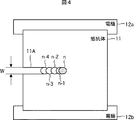
従来、抵抗体のトリミングを行うレーザ加工装置において、固体レーザから出射される周波数、パルス幅、および、ピークパワーが一定のレーザパルスが用いられている。図1は、周波数、パルス幅、および、ピークパワーが一定のレーザパルスを用いて、2つの電極12a,12bの間に設けられている抵抗体11のトリミングを行う様子を模式的に示す図である。この例では、トリミングを行うことにより、電極12aと電極12bとの間の電流が流れる方向に対して垂直な方向(図内横方向)に、幅Wの溝11Aが形成されている。
Conventionally, in a laser processing apparatus that performs trimming of a resistor, a laser pulse having a constant frequency, pulse width, and peak power emitted from a solid-state laser is used. FIG. 1 is a diagram schematically illustrating a state in which trimming of a
また、レーザパルスの周波数が一定なので、図示されているレーザパルスの照射位置n−4乃至nは等間隔となる。すなわち、隣接するレーザパルスの照射位置の間隔であるバイトサイズΔLは一定になる。さらに、レーザパルスのパルス幅およびピークパワーが一定なので、ピークパワー×パルス幅により求められるレーザパルスの加工エネルギーも一定になる。そして、バイトサイズΔLおよび加工エネルギーが一定なので、各レーザパルスによる抵抗値の変化量もほぼ一定になる。 Further, since the frequency of the laser pulse is constant, the irradiation positions n-4 to n of the illustrated laser pulse are equally spaced. That is, the byte size ΔL, which is the interval between the irradiation positions of adjacent laser pulses, is constant. Further, since the pulse width and the peak power of the laser pulse are constant, the processing energy of the laser pulse determined by the peak power × pulse width is also constant. Since the tool size ΔL and the processing energy are constant, the amount of change in resistance value due to each laser pulse is also substantially constant.
ところが、各レーザパルスによる抵抗値の変化量が一定の場合、図2に示されるように、所望のトリミング精度を得られない場合がある。なお、図2は、レーザパルスn−4乃至nが照射されたときの抵抗体11の抵抗値の変化を示すグラフであり、横軸は時間を示し、縦軸は抵抗値を示している。
However, when the amount of change in the resistance value due to each laser pulse is constant, as shown in FIG. FIG. 2 is a graph showing changes in the resistance value of the
この図に示されるように、抵抗体11の抵抗値は、レーザパルスが照射された直後に最も大きく変化し、その後、次のレーザパルスが照射されるまでの間、緩やかに変化する。また、上述したように、バイトサイズΔLおよびレーザパルスの加工エネルギーが一定なので、各レーザパルスによる抵抗値の変化量ΔRa1は、ほぼ一定となる。従って、図2に示されるように、トリミング後の抵抗値の許容範囲が抵抗値Rg1から抵抗値Rg2までの範囲である場合、レーザパルスn−1により抵抗体11の抵抗値が抵抗値Rg1に近い値まで達したとき、レーザパルスnにより抵抗値が抵抗値Rg2を超えてしまい、所望のトリミング精度を得られないときがある。
As shown in this figure, the resistance value of the
一方、変化量ΔRa1が小さくなるように、バイトサイズΔLおよびレーザパルスの加工エネルギーを設定した場合、所望のトリミング精度を得やすくなる一方、トリミングに要する時間が長くなってしまう。 On the other hand, when the byte size ΔL and the processing energy of the laser pulse are set so that the change amount ΔRa1 is small, desired trimming accuracy can be easily obtained, but the time required for trimming becomes long.
そこで、従来、抵抗体11の抵抗値と抵抗値Rg1との差が、変化量ΔRa以下になった場合、レーザパルスの出射間隔を短くし、バイトサイズΔLを短くすることが提案されている(例えば、特許文献1参照)。
Therefore, conventionally, when the difference between the resistance value of the
具体的には、図3に示されるように、レーザパルスn−1を照射した後、抵抗体11の抵抗値と抵抗値Rg1との差がΔRa1以下になった場合、図3および図4に示されるように、レーザパルスの周波数を大きくし、レーザパルスn−1とレーザパルスnの間の時間間隔を短くする。これにより、レーザパルスnにより抵抗体11が加工される(削られる)面積が小さくなり、レーザパルスnによる抵抗値の変化量ΔRa2は、それまでの変化量ΔRa1より小さくなる。従って、より確実に抵抗体11の抵抗値が許容範囲内に収まるように、トリミングを行うことが可能になる。
Specifically, as shown in FIG. 3, when the difference between the resistance value of the
ところで、抵抗体11の抵抗値は、トリミングを行った後も、トリミング後に発生するマイクロクラックにより変化する。例えば、図5に示されるように、トリミングにより抵抗体11に長さXの溝11Aを形成した後、溝11Aの右端から右方向に長さΔXのマイクロクラック11Bが発生し、抵抗体11に形成される切り込み(溝11A+マイクロクラック11B)の長さが長くなり、抵抗体11の抵抗値がΔRbだけ増加する。
By the way, even after trimming, the resistance value of the
一方、抵抗体11に照射されるレーザパルスの加工エネルギーの密度が高いほど、発生するマイクロクラックの量は大きくなり、マイクロクラックによる抵抗値の変化量も大きくなる。特許文献1に記載の発明では、最後の2つのレーザパルスの間隔(バイトサイズΔL)が短くなる分、形成される溝11Aの右端部に照射されるレーザパルスの加工エネルギーの密度も高くなる。従って、特許文献1に記載の発明によりトリミングを行った後の抵抗値の変化量ΔRb2(図3)は、周波数が一定のレーザパルスを用いてトリミングを行った後の抵抗値の変化量ΔRb1(図2)より大きくなる。そのため、図3に示されるように、抵抗体11の抵抗値が、トリミングを行った直後には許容範囲内に収まっていたのに、その後、マイクロクラックにより抵抗値Rg2を超えてしまう場合がある。
On the other hand, the higher the processing energy density of the laser pulse applied to the
本発明は、このような状況に鑑みてなされたものであり、抵抗体のトリミングの精度を向上できるようにするものである。 The present invention has been made in view of such a situation, and is intended to improve the accuracy of trimming of a resistor.
本発明の一側面のレーザ加工装置は、レーザパルスを照射することにより抵抗体の一部を加工し、抵抗体の抵抗値を調整するレーザ加工装置において、レーザパルスを出射するレーザ出射手段と、抵抗体の抵抗値を測定する測定手段と、レーザパルスの出射条件を制御する制御手段とを備え、制御手段は、所定の周波数、パルス幅およびピークパワーである第1の条件でレーザパルスを出射させ、測定手段が測定した抵抗体の抵抗値が所定の閾値以上になったとき、第1の条件と同じ周波数で、かつ、第1の条件よりもパルス幅を広げ、ピークパワーを下げ、加工量がほぼ同等となる程度に加工エネルギーを小さくした第2の条件でレーザパルスを出射させるように制御する。 A laser processing apparatus according to one aspect of the present invention is a laser processing apparatus for processing a part of a resistor by irradiating a laser pulse and adjusting a resistance value of the resistor. A measuring means for measuring the resistance value of the resistor and a control means for controlling the laser pulse emission conditions are provided, and the control means emits a laser pulse under a first condition having a predetermined frequency, pulse width and peak power. It is, when the resistance value of the measuring means to measure the resistor exceeds a predetermined threshold value, at the same frequency as the first condition, and broaden the pulse width than the first condition, lowering the peak power, working Control is performed so that the laser pulse is emitted under the second condition in which the processing energy is reduced to such an extent that the amounts are substantially equal .
本発明の一側面のレーザ加工装置においては、所定の周波数、パルス幅およびピークパワーである第1の条件でレーザパルスが出射され、抵抗体の抵抗値が所定の閾値以上になったとき、第1の条件と同じ周波数で、かつ、第1の条件よりもパルス幅を広げ、ピークパワーを下げ、加工量がほぼ同等となる程度に加工エネルギーを小さくした第2の条件でレーザパルスが出射される。 In the laser processing apparatus according to one aspect of the present invention, when the laser pulse is emitted under the first condition of the predetermined frequency, the pulse width, and the peak power, and the resistance value of the resistor exceeds the predetermined threshold, Laser pulses are emitted under the second condition with the same frequency as the first condition, with the pulse width wider than the first condition, the peak power reduced , and the machining energy reduced to an extent that the machining amount is almost equal. The
従って、抵抗体のトリミングの精度を向上させることができる。 Therefore, the trimming accuracy of the resistor can be improved.
このレーザ加工装置は、例えば、レーザトリミング装置により構成される。このレーザ出射手段は、例えば、ファイバレーザにより構成される。この測定手段は、例えば、抵抗測定器により構成される。この制御手段は、例えば、コンピュータ、または、CPUなどのプロセッサにより構成される。 This laser processing apparatus is constituted by, for example, a laser trimming apparatus. This laser emitting means is constituted by, for example, a fiber laser. This measuring means is constituted by, for example, a resistance measuring instrument. This control means is comprised by processors, such as a computer or CPU, for example.
この制御手段には、抵抗体の大きさおよび抵抗値の目標値に基づいて、レーザパルスのパルス幅およびピークパワーを設定させることができる。 This control means can set the pulse width and peak power of the laser pulse based on the size of the resistor and the target value of the resistance value.
これにより、抵抗体の加工のしやすさ、加工中の抵抗値測定の応答性に応じて、適切なパルス幅およびピークパワーを設定することができ、トリミングに要する時間を短くするとともに、抵抗体のトリミングの精度をより向上させることができる。 This makes it possible to set an appropriate pulse width and peak power according to the ease of processing of the resistor and the responsiveness of resistance measurement during processing, shortening the time required for trimming, and the resistor The trimming accuracy can be further improved.
この制御手段には、抵抗体の大きさおよび抵抗値の目標値に基づいて、抵抗体を加工するスピードおよびレーザパルスの周波数を設定させることができる。 The control means can set the speed of processing the resistor and the frequency of the laser pulse based on the size of the resistor and the target value of the resistance value.
これにより、抵抗体の加工のしやすさ、加工中の抵抗値測定の応答性に応じて、適切な加工スピードおよびレーザパルスの周波数を設定することができ、トリミングに要する時間を短くするとともに、抵抗体のトリミングの精度をより向上させることができる。 This makes it possible to set the appropriate processing speed and the frequency of the laser pulse according to the ease of processing of the resistor and the responsiveness of resistance measurement during processing, shortening the time required for trimming, The accuracy of trimming of the resistor can be further improved.
このレーザ出射手段は、ファイバレーザにより構成することができる。 This laser emitting means can be constituted by a fiber laser.
これにより、レーザパルスの周波数、パルス幅、ピークパワー等を容易に変更することが可能になる。 This makes it possible to easily change the frequency, pulse width, peak power, etc. of the laser pulse.
本発明の一側面のレーザ加工方法は、レーザパルスを照射することにより抵抗体の一部を加工し、抵抗体の抵抗値を調整するレーザ加工装置が、所定の周波数、パルス幅およびピークパワーである第1の条件でレーザパルスを出射し、抵抗体の抵抗値を測定し、測定された抵抗値が所定の閾値以上になったとき、第1の条件と同じ周波数で、かつ、第1の条件よりもパルス幅を広げ、ピークパワーを下げ、加工量がほぼ同等となる程度に加工エネルギーを小さくした第2の条件でレーザパルスを出射するステップを含む。 In the laser processing method according to one aspect of the present invention, a laser processing device that processes a part of a resistor by irradiating a laser pulse and adjusts the resistance value of the resistor has a predetermined frequency, pulse width, and peak power. A laser pulse is emitted under a certain first condition, the resistance value of the resistor is measured, and when the measured resistance value is equal to or greater than a predetermined threshold, the first frequency is the same as the first condition, and the first The method includes a step of emitting a laser pulse under a second condition in which the pulse width is expanded more than the conditions, the peak power is lowered , and the machining energy is reduced to an extent that the machining amount is substantially equal .
本発明の一側面のレーザ加工方法においては、所定の周波数、パルス幅およびピークパワーである第1の条件でレーザパルスが出射され、抵抗体の抵抗値が所定の閾値以上になったとき、第1の条件と同じ周波数で、かつ、第1の条件よりもパルス幅を広げ、ピークパワーを下げ、加工量がほぼ同等となる程度に加工エネルギーを小さくした第2の条件でレーザパルスが出射される。 In the laser processing method according to one aspect of the present invention, when the laser pulse is emitted under the first condition of the predetermined frequency, the pulse width, and the peak power, and the resistance value of the resistor becomes equal to or higher than the predetermined threshold, Laser pulses are emitted under the second condition with the same frequency as the first condition, with the pulse width wider than the first condition, the peak power reduced , and the machining energy reduced to an extent that the machining amount is almost equal. The
従って、抵抗体のトリミングの精度を向上させることができる。 Therefore, the trimming accuracy of the resistor can be improved.
このレーザ加工装置は、例えば、レーザトリミング装置により構成される。 This laser processing apparatus is constituted by, for example, a laser trimming apparatus.
本発明の一側面によれば、抵抗体のトリミングの精度を向上させることができる。 According to one aspect of the present invention, the accuracy of trimming of the resistor can be improved.
以下、図を参照して、本発明の実施の形態について説明する。 Hereinafter, embodiments of the present invention will be described with reference to the drawings.
図6は、本発明を適用したレーザ加工装置の一実施の形態を示すブロック図である。図6のレーザ加工装置101は、例えば、2つの電極104a,104bに挟まれるように基板102上に実装された抵抗体103の一部を加工し、抵抗体103の抵抗値を調整する、いわゆるトリミングを行うことが可能な装置である。なお、抵抗体103は、例えば、チップ抵抗器により構成される。
FIG. 6 is a block diagram showing an embodiment of a laser processing apparatus to which the present invention is applied. The
レーザ加工装置101は、パーソナルコンピュータ(以下、PCと称する)111、トリマ制御部112、ファイバレーザ113、光学部114、および、プローブ115a,115bを含むように構成される。
The
PC111は、図示せぬ入力部を介して入力される抵抗体103に関する情報を取得する。また、PC111は、図示せぬ入力部を介して入力される、抵抗体103の抵抗値の最終的な目標値(以下、目標抵抗値と称する)、および、抵抗体103の加工条件を変更するタイミングを規定するための閾値としての抵抗値(以下、切替変更抵抗値と称する)を取得する。
The
そして、PC111は、抵抗体103のチップサイズ、目標抵抗値、切替変更抵抗値、並びに、図9および図10を参照して後述する、内部に保持している加工条件データに基づいて、抵抗体103の加工条件を設定する。この加工条件は、抵抗体103を加工するスピード、ファイバレーザ113から出射されるレーザパルスの周波数、パルス幅およびピークパワーを少なくとも含む。また、レーザパルスのパルス幅およびピークパワーは、抵抗体103の抵抗値が切替変更抵抗値に達するまでの値と、切替変更抵抗値に達した後の値の少なくとも2種類の値が設定される。
The
PC111は、入力された目標抵抗値および切替変更抵抗値、並びに、設定した加工スピードおよびレーザパルスの周波数を、トリマ制御部112に通知する。また、PC111は、設定したレーザパルスのパルス幅およびピークパワーを、ファイバレーザ113の制御部141に通知する。
The
トリマ制御部112は、ファイバレーザ113および光学部114を制御することにより、レーザパルスの出射タイミングおよび抵抗体103への照射位置を制御する。トリマ制御部112は、測定部131、レーザ制御部132、および、光走査部133を含むように構成される。
The
測定部131は、プローブ115a,115bを介して、電極104a,104bに接続され、電極104a,104bの間の抵抗体103の抵抗値を測定し、測定した抵抗値をレーザ制御部132に通知する。
The
レーザ制御部132は、ファイバレーザ113の制御部141を介して、ファイバレーザ113から出射されるレーザパルスの出射タイミング、並びに、レーザパルスのパルス幅およびピークパワーの変更タイミングを制御する。また、レーザ制御部132は、測定部131により測定された抵抗体103の抵抗値が目標抵抗値に到達したとき、レーザパルスの走査の停止を光走査部133に指令する。
The
光走査部133は、光学部114のドライバ151を介して、ガルバノスキャナ152a,152bによるレーザパルスの走査方向および走査スピードを制御する。
The
ファイバレーザ113は、例えば、希土類元素添加光ファイバにより構成される光ファイバ142をレーザ媒体に用いたファイバレーザである。ファイバレーザ113は、従来の固体レーザと異なり、出射するレーザパルスの周波数、並びに、パルス幅およびピークパワー(=加工エネルギー)を容易かつ高速に変更することが可能である。一方、従来の固体レーザでは、レーザパルスの加工エネルギーを変更するために、アッテネータ等を用いる必要があり、高速に変更することができない。また、従来の固体レーザでは、レーザパルスの周波数の変更は可能であるが、周波数によりパルス幅とピークパワーが一意に決まってしまい、自由度がない。ファイバレーザ113は、これらの従来の固体レーザの弱点を解消したレーザ装置である。
The
ファイバレーザ113は、制御部141、光ファイバ142、および、ヘッド部143を含むように構成される。
The
制御部141は、図示せぬ励起光源を制御して、光ファイバ142を介してヘッド部143から出射されるレーザパルスの周波数、パルス幅、および、ピークパワーを制御する。そして、ヘッド部143から出射されたレーザパルスは、光学部114に入射する。
The
光学部114は、ファイバレーザ113から出射されるレーザパルスを走査するための装置であり、ドライバ151、ガルバノスキャナ152a,152b、および、fθレンズ153を含むように構成される。
The
ガルバノスキャナ152a,152bは、ドライバ151の制御の基に、所定の回転軸を中心に回転し、その回転角により、レーザパルスのfθレンズ153への入射位置および入射角が変化する。そして、fθレンズ153への入射角および入射位置の変化に応じて、抵抗体103の加工面におけるレーザパルスの結像位置が水平方向に移動する。すなわち、ガルバノスキャナ152a,152bにより、レーザパルスの抵抗体103への照射位置がスキャンされる。
The
図7は、トリマ制御部112のレーザ制御部132、および、ファイバレーザ113の制御部141の機能的構成の一例を示すブロック図である。
FIG. 7 is a block diagram illustrating an example of functional configurations of the
レーザ制御部132は、比較設定部171、比較部172、および、トリガパルス発生部173を含むように構成される。
The
比較設定部171は、PC111から通知される目標抵抗値および切替変更抵抗値を比較部172に設定する。
The
比較部172は、測定部131により測定される抵抗体103の抵抗値を、目標抵抗値および切替変更抵抗値と比較する。そして、抵抗体103の抵抗値が切替変更抵抗値に到達したとき、加工条件の変更を、ファイバレーザ113の外部機器インタフェース(INF)部181を介して励起光源制御部182に指令する。また、抵抗体103の抵抗値が目標抵抗値に到達したとき、トリガパルスの停止をトリガパルス発生部173に指令し、レーザパルスの走査の停止を光走査部133に指令する。
The
トリガパルス発生部173は、PC111により設定された周波数のトリガパルスを生成し、ファイバレーザ113の外部機器INF部181を介して励起光源制御部182に供給する。
The trigger
ファイバレーザ113の制御部141は、外部機器INF部181、および、励起光源制御部182を含むように構成される。
The
励起光源制御部182は、外部機器INF部181を介して、レーザパルスのパルス幅およびピークパワーの設定値をPC111から取得する。励起光源制御部182は、トリガパルス発生部173からのトリガパルスに同期して、PC111により設定されたパルス幅およびピークパワーのレーザパルスが、光ファイバ142を介してヘッド部143から出射されるように、図示せぬ励起光源を制御する。また、励起光源制御部182は、トリマ制御部112の比較部172から加工条件の変更の指令を受けた場合、図示せぬ励起光源を制御して、レーザパルスのパルス幅およびピークパワーを変更する。
The excitation light
次に、図8のフローチャートを参照して、レーザ加工装置101により実行されるトリミング処理について説明する。
Next, trimming processing executed by the
ステップS1において、レーザ加工装置101は、加工条件を設定する。具体的には、ユーザは、図示せぬ入力部を介して、目標抵抗値および切替変更抵抗値をPC111に入力する。PC111は、予め作成され、内部に保持している加工条件データを用いて、加工スピード、並びに、レーザパルスの周波数、パルス幅およびピークパワーを設定する。
In step S1, the
図9および図10は、加工条件データの一例を示している。図9は、加工スピード、および、レーザパルスの周波数の設定に用いる加工条件データを示し、図10は、レーザパルスのパルス幅およびピークパワーの設定に用いる加工条件データを示している。なお、図10の各データ欄の上段がレーザパルスのパルス幅を示し、下段がピークパワーを示している。 9 and 10 show an example of the processing condition data. FIG. 9 shows processing condition data used for setting the processing speed and the frequency of the laser pulse, and FIG. 10 shows processing condition data used for setting the pulse width and peak power of the laser pulse. In addition, the upper part of each data column of FIG. 10 shows the pulse width of the laser pulse, and the lower part shows the peak power.
なお、この例では、抵抗体103のチップサイズを大(例えば、1608サイズ程度)、中(例えば、1005サイズ程度)、小(例えば、0603サイズ程度)の3段階に分類し、目標抵抗値を高(例えば、100kΩ以上)、中(例えば、10Ω以上100kΩ未満)、低(10Ω未満)の3段階に分類し、抵抗体103のチップサイズ3種類×目標抵抗値3種類の合計9種類の組み合わせに対して、それぞれ個別にデータが設定されている。
In this example, the chip size of the
ここで、加工条件データの各項目について見ていくと、加工スピードは、抵抗体103の加工のしやすさ(以下、加工性と称する)と、抵抗値を測定する際の応答性(以下、測定応答性と称する)とのバランスを考慮して、目標抵抗値が中レベルの場合、目標抵抗値が低レベルおよび高レベルの場合と比較して速くなるように設定されている。ただし、抵抗体103のチップサイズが小レベルの場合、目標抵抗値の大きさにかかわらず、全て同じスピードに設定されている。
Here, looking at each item of the processing condition data, the processing speed is determined by the ease of processing of the resistor 103 (hereinafter referred to as processability) and the response when measuring the resistance value (hereinafter, In consideration of the balance with measurement responsiveness), the target resistance value is set to be faster when the target resistance value is at a medium level than when the target resistance value is at a low level and at a high level. However, when the chip size of the
なお、一般的に、抵抗体103は、チップサイズが同じ場合、目標抵抗値が高くなるほど、加工性が良くなる一方、測定応答性が悪くなり、目標抵抗値が低くなるほど、加工性が悪くなる一方、測定応答性が良くなる。
In general, for the
レーザパルスの周波数は、抵抗体103の加工性と測定応答性とのバランスを考慮して、目標抵抗値が中レベルの場合、最も大きく、目標抵抗値が高レベルの場合、最も小さくなるように設定されている。ただし、抵抗体103のチップサイズが小レベルの場合、目標抵抗値の大きさにかかわらず、全て同じ周波数に設定されている。
Considering the balance between the workability of the
なお、バイトサイズは、加工スピード÷レーザパルスの周波数により求めることができる。 The byte size can be obtained by processing speed ÷ laser pulse frequency.
レーザパルスのパルス幅は、全ての抵抗体103のチップサイズおよび目標抵抗値の組み合わせにおいて、70ns、110ns、150ns、170ns、230nsの5種類が設定されている。なお、以下、図10に示されるように、レーザパルスの波形について、パルス幅が70nsの波形を波形Aと称し、パルス幅が110nsの波形を波形Bと称し、パルス幅が150nsの波形を波形Cと称し、パルス幅が170nsの波形を波形Dと称し、パルス幅が230nsの波形を波形Eと称する。
As for the pulse width of the laser pulse, five types of 70 ns, 110 ns, 150 ns, 170 ns, and 230 ns are set for combinations of chip sizes and target resistance values of all the
また、抵抗体103のチップサイズと目標抵抗値、および、パルス幅の各組み合わせに対して、それぞれピークパワーが設定されている。
In addition, peak power is set for each combination of the chip size, the target resistance value, and the pulse width of the
なお、ファイバレーザ113の単位時間あたりのパワーは、レーザパルスのピークパワー×パルス幅×周波数により求めることができるが、抵抗体103の加工性を考慮して、同じチップサイズの場合、目標抵抗値が低レベルのとき、最も大きく、目標抵抗値が高レベルのとき、最も小さくなるように設定されている。ただし、抵抗体103のチップサイズが小レベルの場合、目標抵抗値の大きさにかかわらず、全て同じパワーに設定されている。
The power per unit time of the
また、レーザパルス1つ当たりの加工エネルギーは、ピークパワー×パルス幅により求められるが、同じチップサイズおよび目標抵抗値の場合、パルス幅が狭くなるほど、ピークパワーが大きく、パルス幅が広くなるほど、ピークパワーが小さくなるように、加工エネルギーが設定されている。 In addition, the processing energy per laser pulse is obtained by peak power × pulse width. For the same chip size and target resistance value, the peak power increases as the pulse width decreases, and the peak increases as the pulse width increases. Processing energy is set so that the power is reduced.
図11は、図10の加工条件データに基づいて、抵抗体103のチップサイズと目標抵抗値の組み合わせと、設定されるレーザパルスのパルス幅とピークパワーの組み合わせとの関係をまとめた表である。例えば、抵抗体103のチップサイズが大レベル、かつ、目標抵抗値が高レベルの場合に設定されるレーザパルスのパルス幅とピークパワーの組み合わせは、図内で「サイズ大 抵抗値高」と記載されている欄に対応する組み合わせとなる。すなわち、抵抗体103のチップサイズが大レベル、かつ、目標抵抗値が高レベルの場合、設定されるレーザパルスのパルス幅とピークパワーは、パルス幅70nmおよびピークパワー4.0kW、パルス幅110nmおよびピークパワー2.7kW、パルス幅150nmおよびピークパワー2.0kW、パルス幅170nmおよびピークパワー1.8kW、パルス幅230nmおよびピークパワー1.3kWのいずれかの組み合わせとなる。
FIG. 11 is a table summarizing the relationship between the combination of the chip size of the
ところで、レーザパルスの加工エネルギーが同じでも、パルス幅およびピークパワーが異なる場合、レーザパルスによる抵抗体103の抵抗値の変化は異なる。
By the way, even if the processing energy of the laser pulse is the same, when the pulse width and the peak power are different, the change in the resistance value of the
図12の左側のグラフは、周波数および加工エネルギーが同じで、パルス幅およびピークパワーが異なるレーザパルスを用いて、同じ一定の加工スピードでトリミングを行った場合の抵抗体103の抵抗値の変化の例を示す図である。なお、図12の左側のグラフの横軸は時間を示し、縦軸は抵抗値を示している。また、図12の左側のグラフの縦の点線より左側の領域は、トリミング中の抵抗体103の抵抗値の変化を示し、点線より右側の領域はトリミング後の抵抗体103の抵抗値の変化を示している。なお、加工スピードが一定なので、図12の左側のグラフのトリミング中の領域において、横軸方向を、トリミングにより抵抗体103に形成される溝の距離(=加工スピード×時間)に読み替えることが可能である。
The graph on the left side of FIG. 12 shows changes in the resistance value of the
また、図12の左側のグラフの線201は、図12の右側のいちばん上の波形のレーザパルスを用いた場合の抵抗値の変化を示しており、線202は、図12の右側のまん中の波形のレーザパルスを用いた場合の抵抗値の変化を示しており、線203は、図12の右側のいちばん下の波形のレーザパルスを用いた場合の抵抗値の変化を示している。なお、図12の右側の各グラフの横軸は時間を示し、縦軸はパワーを示している。また、値Pcは、抵抗体103を加工するのに必要なパワーの最小値(加工しきい値)を示している。
Also, a
従って、線201は、パルス幅が小さく、ピークパワーが大きいレーザパルスを用いた場合の抵抗値の変化を示し、線202は、パルス幅およびピークパワーとも中程度のレーザパルスを用いた場合の抵抗値の変化を示し、線203は、パルス幅が大きく、ピークパワーが小さいレーザパルスを用いた場合の抵抗値の変化を示している。
Therefore, a
図12の左側のグラフに示されるように、レーザパルスの加工エネルギーが同じ場合、ピークパワーが大きく、パルス幅が小さくなるほど、レーザパルス1つあたりの加工量が小さくなり、トリミング中の抵抗値の変化が小さくなる一方、加工エネルギーの密度が高くなり、抵抗体103にマイクロクラックが発生しやくすなるため、トリミング後の抵抗値の変化は大きくなる。マイクロクラックは、溶融した抵抗体103が凝固する際に生じるストレスと抵抗体103の部分的切断によって平衡状態が崩れ、切断部先端に集中したストレスにより発生する。パルス幅が小さくピークパワーが大きい場合、溶融と凝固の時間が短くストレスによるマイクロクラックが発生する原因となりやすい。
As shown in the graph on the left side of FIG. 12, when the processing energy of the laser pulse is the same, as the peak power increases and the pulse width decreases, the processing amount per laser pulse decreases, and the resistance value during trimming is reduced. While the change becomes smaller, the density of the processing energy becomes higher and microcracks are more likely to occur in the
一方、ピークパワーが小さく、パルス幅が大きくなるほど、レーザパルス1つ当たりの加工量が大きくなり、トリミング中の抵抗値の変化が大きくなる一方、加工エネルギーの密度が低くなり、抵抗体103のマイクロクラックの発生が抑制されるため、トリミング後の抵抗値の変化は小さくなる。
On the other hand, the smaller the peak power and the larger the pulse width, the larger the processing amount per laser pulse and the greater the change in resistance during trimming, while the lower the processing energy density, and the
図8に戻り、ステップS1において、PC111は、図9の加工条件データ、並びに、抵抗体103のチップサイズおよび目標抵抗値に基づいて、加工スピードおよびレーザパルスの周波数を決定する。
Returning to FIG. 8, in step S <b> 1, the
また、PC111は、抵抗体103のチップサイズ、目標抵抗値、並びに、切替変更抵抗値に基づいて、抵抗体103の抵抗値が切替変更抵抗値に到達するまで使用するレーザパルスの波形(以下、変更前波形とも称する)、および、抵抗体103の抵抗値が切替変更抵抗値に到達した後に使用するレーザパルスの波形(以下、変更後波形とも称する)を選択する。これにより、抵抗体103の抵抗値が切替変更抵抗値に到達する前のレーザパルスのパルス幅およびピークパワー、到達した後のレーザパルスのパルス幅およびピークパワーが決定する。
Further, the
なお、変更後波形の選択は、目標抵抗値によりおおよそ決定することができる。具体的には、目標抵抗値が小さい抵抗体103では、抵抗体103そのもの加工性が良くないため高いピークパワーが必要となる。従って、切替変更抵抗値に到達した後の変更後波形は、変更前波形からピークパワーをあまり変えず、パルス幅を短めにする方法が有効である。一方、目標抵抗値が高い場合は、抵抗体103の加工性が良いため、変更前波形からピークパワーを下げ、パルス幅を長くする方法が有効である。どちらも加工エネルギーは小さくなる。
The selection of the changed waveform can be roughly determined by the target resistance value. Specifically, the
ここで、PC111は、波形を変更する前より変更した後の方が、パルス幅が広くなり、かつ、レーザパルス1つあたりのトリミング中の抵抗体103の抵抗値の変化量(すなわち、1つのレーザパルスにより形成される溝のみによる抵抗値の変化量)が小さくなるように、変更前波形および変更後波形を選択する。従って、少なくとも、波形を変更する前より変更した後の方が、パルス幅が広くなり、ピークパワーが小さくなり、加工エネルギーが小さくなる。
Here, the
PC111は、ユーザにより入力された目標抵抗値および切替変更抵抗値をトリマ制御部112の比較設定部171に通知する。比較設定部171は、通知された目標抵抗値および切替変更抵抗値を比較部172に設定する。また、PC111は、決定したレーザパルスの周波数をトリマ制御部112のトリガパルス発生部173に通知する。さらに、PC111は、決定した加工スピードをトリマ制御部112の光走査部133に通知する。また、PC111は、決定した変更前波形および変更後波形を、外部機器INF部181を介して、励起光源制御部182に通知する。
The
ステップS2において、レーザ加工装置101は、加工を開始する。具体的には、トリガパルス発生部173は、PC111により設定された周波数のトリガパルスを生成し、外部機器INF部181を介して励起光源制御部182に供給する処理を開始する。
In step S2, the
励起光源制御部182は、トリガパルス発生部173からのトリガパルスに同期して、PC111により設定された変更前波形のレーザパルスが、光ファイバ142を介してヘッド部143から出射されるように、図示せぬ励起光源を制御する処理を開始する。
The excitation light
光走査部133は、ガルバノスキャナ152a,152bにより抵抗体103の加工面において所定の加工方向にレーザパルスを走査するスピードが、PC111により設定された加工スピードになるように、光学部114のドライバ151を制御する処理を開始する。
The
測定部131は、プローブ115a,115bを介して抵抗体103の抵抗値を測定し、比較部172に通知する処理を開始する。
The
これにより、設定された周波数および変更前波形のレーザパルスを用いて、設定された加工スピードで抵抗体103のトリミングを行いながら、抵抗体103の抵抗値を測定する処理が開始される。
Thereby, the process of measuring the resistance value of the
ステップS3において、比較部172は、切替変更抵抗値に到達したか否かを判定する。具体的には、比較部172は、測定部131により測定された抵抗体103の抵抗値と切替変更抵抗値とを比較する。そして、比較部172は、抵抗体103の抵抗値が切替変更抵抗値未満である場合、まだ切替変更抵抗値に到達していないと判定し、切替変更抵抗値に到達したと判定するまで、所定の間隔でステップS3の判定処理を繰り返す。
In step S3, the
一方、ステップS3において、比較部172は、抵抗体103の抵抗値が切替変更抵抗値以上である場合、切替変更抵抗値に到達したと判定し、処理はステップS4に進む。
On the other hand, if the resistance value of the
ステップS4において、レーザ加工装置101は、加工条件を変更する。具体的には、比較部172は、加工条件の変更を、外部機器INF部181を介して励起光源制御部182に指令する。励起光源制御部182は、光ファイバ142を介してヘッド部143から出射されるレーザパルスの波形が、PC111により設定された変更後波形になるように、図示せぬ励起光源を制御する。これにより、加工スピードおよびレーザパルスの周波数を変えずに一定に保ったまま、変更後波形のレーザパルスを用いて抵抗体103のトリミングを行う処理が開始される。
In step S4, the
ステップS5において、比較部172は、目標抵抗値に到達したか否かを判定する。具体的には、比較部172は、測定部131により測定された抵抗体103の抵抗値と目標抵抗値とを比較する。そして、比較部172は、抵抗体103の抵抗値が目標抵抗値未満である場合、まだ目標抵抗値に到達していないと判定し、目標抵抗値に到達したと判定するまで、所定の間隔でステップS5の判定処理を繰り返す。
In step S5, the
一方、ステップS5において、比較部172は、抵抗体103の抵抗値が目標抵抗値以上である場合、目標抵抗値に到達したと判定し、処理はステップS6に進む。
On the other hand, in step S5, when the resistance value of the
ステップS6において、レーザ加工装置101は、加工を終了する。具体的には、比較部172は、トリガパルスの停止をトリガパルス発生部173に指令し、トリガパルス発生部173は、ファイバレーザ113へのトリガパルスの供給を停止する。これにより、ファイバレーザ113からのレーザパルスの出射が停止する。また、比較部172は、レーザパルスの走査の停止を光走査部133に指令する。光走査部133は、ガルバノスキャナ152a,152bの動作を停止するようドライバ151を制御する。
In step S6, the
その後、トリミング処理は終了する。 Thereafter, the trimming process ends.
ここで、図13および図14を参照して、本発明の効果について説明する。なお、以下、目標抵抗値が抵抗値Rg11に設定され、トリミング後の抵抗値の許容範囲が抵抗値Rg11から抵抗値Rg12までの範囲に設定され、切替変更抵抗値が抵抗値Rcに設定されているものとする。 Here, the effects of the present invention will be described with reference to FIGS. Hereinafter, the target resistance value is set to the resistance value Rg11, the allowable range of the resistance value after trimming is set to the range from the resistance value Rg11 to the resistance value Rg12, and the switching change resistance value is set to the resistance value Rc. It shall be.
図13に示されるように、レーザパルスn−1を照射した後、抵抗体103の抵抗値が切替変更抵抗値Rcを超えた場合、レーザパルスn−1と比較して、パルス幅が広く、ピークパワーが小さく、加工エネルギーが小さいレーザパルスnが、それまでと同じ時間間隔で照射される。また、上述したように、レーザパルスnによるトリミング中の抵抗体103の抵抗値の変化量ΔRa12が、それまでのレーザパルスによる変化量ΔRa11より小さくなるように、レーザパルスnの波形が設定されている。従って、抵抗体103の抵抗値を、より目標抵抗値Rg11に近づけることが可能になる。
As shown in FIG. 13, when the resistance value of the
また、図14に示されるように、レーザパルスn−1とレーザパルスnとの間のバイトサイズが、それまでのバイトサイズと変わらない一方で、パルス幅が広くなることにより、レーザパルスnの加工量は、加工エネルギーが小さくなったにも関わらず、レーザパルスn−1までの加工量とほぼ同等となる。また、ピークパワーが小さくなることにより、レーザパルスnの加工エネルギーの密度は、レーザパルスn−1までの加工エネルギーの密度より低くなる。従って、抵抗体103に形成された溝103Aの右端から右方向(すなわち、溝103Aが伸びる方向)に発生するマイクロクラックの量を少なくし、トリミング後の抵抗体103の抵抗値の変化量ΔRb11を小さくすることができる。
Further, as shown in FIG. 14, the byte size between the laser pulse n-1 and the laser pulse n is not different from the previous byte size, but the pulse width is widened. The processing amount is substantially equal to the processing amount up to the laser pulse n−1, although the processing energy is reduced. Further, as the peak power becomes smaller, the density of the processing energy of the laser pulse n becomes lower than the density of the processing energy up to the laser pulse n-1. Therefore, the amount of microcracks generated in the right direction from the right end of the
従って、抵抗体103の抵抗値を、より確実に許容範囲内に収めることができるとともに、目標抵抗値Rg11により近い値に調整することができる。
Therefore, the resistance value of the
また、レーザ加工装置101では、上述したように、レーザパルスの周波数を変更する必要がないため、レーザパルスの周波数の変更に伴う加工スピードの調整が不要である。従って、加工スピードの変更が間に合わずに、レーザパルスがほぼ同じ位置に繰り返し照射される、いわゆる加工溜まりが発生したり、隣接するレーザパルスが重ならず、間に未加工の領域ができる、いわゆる加工離れが発生したりすることが防止される。
Further, in the
このように、レーザ加工装置101によれば、抵抗体103のトリミングの精度を向上させることができる。
Thus, according to the
なお、図13および図14では、加工条件を変更した後のレーザパルスが1回のみ照射される例を示したが、2回以上照射されるように切替変更抵抗値を設定するようにしてもよい。 13 and 14 show an example in which the laser pulse after changing the processing condition is irradiated only once. However, the switching change resistance value may be set so that the laser pulse is irradiated twice or more. Good.
また、以上の説明では、加工条件を1回のみ変更する例を示したが、切替変更抵抗値を2つ以上設定して、加工条件を2回以上変更するようにしてもよい。なお、加工条件を2回以上変更する場合も、加工条件を変更する度に、レーザパルスのパルス幅が広くなり、かつ、レーザパルス1つあたりのトリミング中の抵抗体の抵抗値の変化量が小さくなるように、レーザパルスの波形を設定するようにすればよい。 In the above description, an example in which the machining condition is changed only once has been described. However, two or more switching change resistance values may be set and the machining condition may be changed twice or more. Even when the machining conditions are changed twice or more, each time the machining conditions are changed, the pulse width of the laser pulse is widened, and the amount of change in the resistance value of the resistor during trimming per laser pulse is increased. What is necessary is just to set the waveform of a laser pulse so that it may become small.
さらに、PC111、トリマ制御部112、および、ファイバレーザ113の制御部141の構成および処理の分担は、上述した例に限定されるものではない。例えば、PC111の処理の一部または全部をトリマ制御部112が実行するようにしたり、PC111、トリマ制御部112、および、ファイバレーザ113の制御部141を1つの装置にまとめるようにしたりすることも可能である。
Furthermore, the configuration of the
さらに、上述したPC111、トリマ制御部112、および、ファイバレーザ113の制御部141の一連の処理は、ハードウエアにより実行することもできるし、ソフトウエアにより実行することもできる。一連の処理をソフトウエアにより実行する場合には、そのソフトウエアを構成するプログラムが、コンピュータにインストールされる。ここで、コンピュータには、専用のハードウエアに組み込まれているコンピュータや、各種のプログラムをインストールすることで、各種の機能を実行することが可能な、例えば汎用のパーソナルコンピュータなどが含まれる。
Furthermore, a series of processes of the
図15は、上述した一連の処理をプログラムにより実行するコンピュータのハードウエアの構成例を示すブロック図である。 FIG. 15 is a block diagram illustrating a configuration example of hardware of a computer that executes the above-described series of processing by a program.
コンピュータにおいて、CPU(Central Processing Unit)301,ROM(Read Only Memory)302,RAM(Random Access Memory)303は、バス304により相互に接続されている。
In a computer, a CPU (Central Processing Unit) 301, a ROM (Read Only Memory) 302, and a RAM (Random Access Memory) 303 are connected to each other by a
バス304には、さらに、入出力インタフェース305が接続されている。入出力インタフェース305には、入力部306、出力部307、記憶部308、通信部309、及びドライブ310が接続されている。
An input /
入力部306は、キーボード、マウス、マイクロフォンなどよりなる。出力部307は、ディスプレイ、スピーカなどよりなる。記憶部308は、ハードディスクや不揮発性のメモリなどよりなる。通信部309は、ネットワークインタフェースなどよりなる。ドライブ310は、磁気ディスク、光ディスク、光磁気ディスク、又は半導体メモリなどのリムーバブルメディア311を駆動する。
The
以上のように構成されるコンピュータでは、CPU301が、例えば、記憶部308に記憶されているプログラムを、入出力インタフェース305及びバス304を介して、RAM303にロードして実行することにより、上述した一連の処理が行われる。
In the computer configured as described above, the
コンピュータ(CPU301)が実行するプログラムは、例えば、パッケージメディア等としてのリムーバブルメディア311に記録して提供することができる。また、プログラムは、ローカルエリアネットワーク、インターネット、デジタル衛星放送といった、有線または無線の伝送媒体を介して提供することができる。
The program executed by the computer (CPU 301) can be provided by being recorded on a
コンピュータでは、プログラムは、リムーバブルメディア311をドライブ310に装着することにより、入出力インタフェース305を介して、記憶部308にインストールすることができる。また、プログラムは、有線または無線の伝送媒体を介して、通信部309で受信し、記憶部308にインストールすることができる。その他、プログラムは、ROM302や記憶部308に、あらかじめインストールしておくことができる。
In the computer, the program can be installed in the
なお、コンピュータが実行するプログラムは、本明細書で説明する順序に沿って時系列に処理が行われるプログラムであっても良いし、並列に、あるいは呼び出しが行われたとき等の必要なタイミングで処理が行われるプログラムであっても良い。 The program executed by the computer may be a program that is processed in time series in the order described in this specification, or in parallel or at a necessary timing such as when a call is made. It may be a program for processing.
また、本発明の実施の形態は、上述した実施の形態に限定されるものではなく、本発明の要旨を逸脱しない範囲において種々の変更が可能である。 The embodiments of the present invention are not limited to the above-described embodiments, and various modifications can be made without departing from the scope of the present invention.
101 レーザ加工装置
103 抵抗体
111 パーソナルコンピュータ
112 トリマ制御部
113 ファイバレーザ
114 光学部
115a,115b プローブ
131 測定部
132 レーザ制御部
133 光走査部
141 制御部
142 光ファイバ
143 ヘッド部
151 ドライバ
152a,152b ガルバノスキャナ
153 fθレンズ
171 比較測定部
172 比較部
173 トリガパルス発生部
182 励起光源制御部
DESCRIPTION OF
Claims (5)
前記レーザパルスを出射するレーザ出射手段と、
前記抵抗体の抵抗値を測定する測定手段と、
前記レーザパルスの出射条件を制御する制御手段と
を備え、
前記制御手段は、
所定の周波数、パルス幅およびピークパワーである第1の条件で前記レーザパルスを出射させ、
前記測定手段が測定した前記抵抗体の抵抗値が所定の閾値以上になったとき、前記第1の条件と同じ周波数で、かつ、前記第1の条件よりもパルス幅を広げ、ピークパワーを下げ、加工量がほぼ同等となる程度に加工エネルギーを小さくした第2の条件で前記レーザパルスを出射させるように制御する
ことを特徴するレーザ加工装置。 In a laser processing apparatus for processing a part of a resistor by irradiating a laser pulse and adjusting a resistance value of the resistor,
Laser emitting means for emitting the laser pulse;
Measuring means for measuring the resistance value of the resistor;
Control means for controlling the emission condition of the laser pulse,
The control means includes
The laser pulse is emitted under a first condition having a predetermined frequency, pulse width, and peak power,
When the resistance value of the resistor measured by the measuring means is equal to or higher than a predetermined threshold, the pulse width is broadened and the peak power is lowered at the same frequency as the first condition and more than the first condition. The laser processing apparatus is characterized in that the laser pulse is controlled to be emitted under a second condition in which the processing energy is reduced to an extent that the processing amount is substantially equal .
ことを特徴とする請求項1に記載のレーザ加工装置。 The laser processing apparatus according to claim 1, wherein the control unit sets a pulse width and a peak power of the laser pulse based on a size of the resistor and a target value of the resistance value.
ことを特徴とする請求項1に記載のレーザ加工装置。 2. The laser processing according to claim 1, wherein the control unit sets the speed of processing the resistor and the frequency of the laser pulse based on a size of the resistor and a target value of the resistance value. 3. apparatus.
ことを特徴とする請求項1に記載のレーザ加工装置。 The laser processing apparatus according to claim 1, wherein the laser emitting unit is a fiber laser.
所定の周波数、パルス幅およびピークパワーである第1の条件で前記レーザパルスを出射し、
前記抵抗体の抵抗値を測定し、
前記測定された抵抗値が所定の閾値以上になったとき、前記第1の条件と同じ周波数で、かつ、前記第1の条件よりもパルス幅を広げ、ピークパワーを下げ、加工量がほぼ同等となる程度に加工エネルギーを小さくした第2の条件で前記レーザパルスを出射する
ステップを含むことを特徴するレーザ加工方法。 A laser processing apparatus that processes a part of the resistor by irradiating a laser pulse and adjusts the resistance value of the resistor,
Emitting the laser pulse under a first condition of a predetermined frequency, pulse width and peak power;
Measure the resistance value of the resistor,
When the measured resistance value is equal to or greater than a predetermined threshold value, the same frequency as the first condition, the pulse width is widened than the first condition, the peak power is lowered , and the processing amount is almost equal. A laser processing method comprising: emitting the laser pulse under a second condition in which processing energy is reduced to such an extent that
Priority Applications (1)
| Application Number | Priority Date | Filing Date | Title |
|---|---|---|---|
| JP2009228004A JP5310452B2 (en) | 2009-09-30 | 2009-09-30 | Laser processing apparatus and laser processing method |
Applications Claiming Priority (1)
| Application Number | Priority Date | Filing Date | Title |
|---|---|---|---|
| JP2009228004A JP5310452B2 (en) | 2009-09-30 | 2009-09-30 | Laser processing apparatus and laser processing method |
Publications (2)
| Publication Number | Publication Date |
|---|---|
| JP2011077336A JP2011077336A (en) | 2011-04-14 |
| JP5310452B2 true JP5310452B2 (en) | 2013-10-09 |
Family
ID=44021001
Family Applications (1)
| Application Number | Title | Priority Date | Filing Date |
|---|---|---|---|
| JP2009228004A Active JP5310452B2 (en) | 2009-09-30 | 2009-09-30 | Laser processing apparatus and laser processing method |
Country Status (1)
| Country | Link |
|---|---|
| JP (1) | JP5310452B2 (en) |
Families Citing this family (4)
| Publication number | Priority date | Publication date | Assignee | Title |
|---|---|---|---|---|
| JP5609370B2 (en) * | 2010-07-23 | 2014-10-22 | 船井電機株式会社 | Image display device |
| US20140175684A1 (en) * | 2012-12-20 | 2014-06-26 | Apple Inc. | Methods and Equipment for Trimming Polarizers in Displays |
| JP6792484B2 (en) * | 2017-02-24 | 2020-11-25 | Koa株式会社 | Chip resistors and their manufacturing methods |
| CN109994295A (en) * | 2019-04-18 | 2019-07-09 | 深圳市杰普特光电股份有限公司 | The resistance trimming method and system of resistor body |
Family Cites Families (6)
| Publication number | Priority date | Publication date | Assignee | Title |
|---|---|---|---|---|
| JPS5726408A (en) * | 1980-07-23 | 1982-02-12 | Nippon Electric Co | Laser trimming device |
| JPH0712695B2 (en) * | 1987-01-20 | 1995-02-15 | 松下電器産業株式会社 | Thermal head trimming method for heating resistor |
| JP3543731B2 (en) * | 2000-05-15 | 2004-07-21 | 日本電気株式会社 | Laser trimming method and laser trimming apparatus |
| JP2002361448A (en) * | 2001-06-11 | 2002-12-18 | Nec Corp | Laser irradiation device and method for controlling passage of laser beam in the laser irradiation device |
| JP2004001345A (en) * | 2002-03-27 | 2004-01-08 | Kyocera Corp | Ink jet head and ink jet printer using the same |
| JP2008135426A (en) * | 2006-11-27 | 2008-06-12 | Matsushita Electric Ind Co Ltd | Resistor laser trimming method and laser trimming apparatus used therefor |
-
2009
- 2009-09-30 JP JP2009228004A patent/JP5310452B2/en active Active
Also Published As
| Publication number | Publication date |
|---|---|
| JP2011077336A (en) | 2011-04-14 |
Similar Documents
| Publication | Publication Date | Title |
|---|---|---|
| JP5310452B2 (en) | Laser processing apparatus and laser processing method | |
| JP5082798B2 (en) | LASER OSCILLATION DEVICE AND ITS CONTROL METHOD | |
| KR101387314B1 (en) | Pulsed laser system and driving method thereof | |
| JP5603324B2 (en) | Laser pulse equalization system and method | |
| JP2005523583A5 (en) | ||
| US7705268B2 (en) | Method and system for laser soft marking | |
| TW201034781A (en) | Minimizing thermal effect during material removal using a laser | |
| WO2019176753A1 (en) | Laser power control device, laser processing device, and laser power control method | |
| JP6551271B2 (en) | Optical amplification apparatus and laser processing apparatus | |
| JP2019104046A5 (en) | ||
| JP2008515634A (en) | A method to provide stable quality for removal of target material by laser with different output characteristics | |
| US10919110B2 (en) | Data generating device setting machining condition suitable for foil placed on workpiece to be machined by irradiating laser beam thereon | |
| JP6713203B2 (en) | Laser processing equipment | |
| JP2016016449A (en) | Laser processing machine, control method for the same, and manufacturing method of spark plug | |
| JP5988903B2 (en) | Laser processing apparatus and laser processing method | |
| JP6502993B2 (en) | LASER DEVICE WITH MULTIPLE LASER MODULES | |
| JP6385997B2 (en) | Laser welding method and laser welding apparatus | |
| JP6184798B2 (en) | Gas laser device, pulse laser beam output method, and laser processing apparatus | |
| WO2010103657A1 (en) | Laser machining apparatus | |
| KR20200063044A (en) | Laser Processing Apparatus and Processing Method of Processed Products | |
| JP2015509049A (en) | Material processing method and material processing apparatus using pulse laser beam generated by fiber laser | |
| JP2013197131A (en) | Semiconductor laser driving device, method for driving semiconductor laser and electronic equipment | |
| KR20200129025A (en) | Multi-laser cutting method and system thereof | |
| JP2008194709A (en) | Laser processing method | |
| US9083146B1 (en) | Solid state laser device |
Legal Events
| Date | Code | Title | Description |
|---|---|---|---|
| A621 | Written request for application examination |
Free format text: JAPANESE INTERMEDIATE CODE: A621 Effective date: 20120302 |
|
| A977 | Report on retrieval |
Free format text: JAPANESE INTERMEDIATE CODE: A971007 Effective date: 20130314 |
|
| A131 | Notification of reasons for refusal |
Free format text: JAPANESE INTERMEDIATE CODE: A131 Effective date: 20130319 |
|
| A521 | Request for written amendment filed |
Free format text: JAPANESE INTERMEDIATE CODE: A523 Effective date: 20130520 |
|
| TRDD | Decision of grant or rejection written | ||
| A01 | Written decision to grant a patent or to grant a registration (utility model) |
Free format text: JAPANESE INTERMEDIATE CODE: A01 Effective date: 20130604 |
|
| A61 | First payment of annual fees (during grant procedure) |
Free format text: JAPANESE INTERMEDIATE CODE: A61 Effective date: 20130617 |
|
| R150 | Certificate of patent or registration of utility model |
Free format text: JAPANESE INTERMEDIATE CODE: R150 Ref document number: 5310452 Country of ref document: JP Free format text: JAPANESE INTERMEDIATE CODE: R150 |
|
| S111 | Request for change of ownership or part of ownership |
Free format text: JAPANESE INTERMEDIATE CODE: R313113 |
|
| R350 | Written notification of registration of transfer |
Free format text: JAPANESE INTERMEDIATE CODE: R350 |
|
| R250 | Receipt of annual fees |
Free format text: JAPANESE INTERMEDIATE CODE: R250 |
|
| R250 | Receipt of annual fees |
Free format text: JAPANESE INTERMEDIATE CODE: R250 |
|
| R250 | Receipt of annual fees |
Free format text: JAPANESE INTERMEDIATE CODE: R250 |
|
| R250 | Receipt of annual fees |
Free format text: JAPANESE INTERMEDIATE CODE: R250 |
|
| R250 | Receipt of annual fees |
Free format text: JAPANESE INTERMEDIATE CODE: R250 |
|
| R250 | Receipt of annual fees |
Free format text: JAPANESE INTERMEDIATE CODE: R250 |
|
| R250 | Receipt of annual fees |
Free format text: JAPANESE INTERMEDIATE CODE: R250 |