JP4851592B2 - Dual inductor circuit for multi-band - Google Patents
Dual inductor circuit for multi-band Download PDFInfo
- Publication number
- JP4851592B2 JP4851592B2 JP2009522988A JP2009522988A JP4851592B2 JP 4851592 B2 JP4851592 B2 JP 4851592B2 JP 2009522988 A JP2009522988 A JP 2009522988A JP 2009522988 A JP2009522988 A JP 2009522988A JP 4851592 B2 JP4851592 B2 JP 4851592B2
- Authority
- JP
- Japan
- Prior art keywords
- inductor
- frequency band
- circuit
- mixer
- terminal
- Prior art date
- Legal status (The legal status is an assumption and is not a legal conclusion. Google has not performed a legal analysis and makes no representation as to the accuracy of the status listed.)
- Expired - Fee Related
Links
Images


Classifications
-
- H—ELECTRICITY
- H10—SEMICONDUCTOR DEVICES; ELECTRIC SOLID-STATE DEVICES NOT OTHERWISE PROVIDED FOR
- H10D—INORGANIC ELECTRIC SEMICONDUCTOR DEVICES
- H10D89/00—Aspects of integrated devices not covered by groups H10D84/00 - H10D88/00
-
- H—ELECTRICITY
- H10—SEMICONDUCTOR DEVICES; ELECTRIC SOLID-STATE DEVICES NOT OTHERWISE PROVIDED FOR
- H10D—INORGANIC ELECTRIC SEMICONDUCTOR DEVICES
- H10D84/00—Integrated devices formed in or on semiconductor substrates that comprise only semiconducting layers, e.g. on Si wafers or on GaAs-on-Si wafers
-
- H—ELECTRICITY
- H01—ELECTRIC ELEMENTS
- H01F—MAGNETS; INDUCTANCES; TRANSFORMERS; SELECTION OF MATERIALS FOR THEIR MAGNETIC PROPERTIES
- H01F17/00—Fixed inductances of the signal type
- H01F17/0006—Printed inductances
-
- H—ELECTRICITY
- H01—ELECTRIC ELEMENTS
- H01F—MAGNETS; INDUCTANCES; TRANSFORMERS; SELECTION OF MATERIALS FOR THEIR MAGNETIC PROPERTIES
- H01F21/00—Variable inductances or transformers of the signal type
- H01F21/12—Variable inductances or transformers of the signal type discontinuously variable, e.g. tapped
-
- H—ELECTRICITY
- H10—SEMICONDUCTOR DEVICES; ELECTRIC SOLID-STATE DEVICES NOT OTHERWISE PROVIDED FOR
- H10P—GENERIC PROCESSES OR APPARATUS FOR THE MANUFACTURE OR TREATMENT OF DEVICES COVERED BY CLASS H10
- H10P95/00—Generic processes or apparatus for manufacture or treatments not covered by the other groups of this subclass
-
- H—ELECTRICITY
- H01—ELECTRIC ELEMENTS
- H01F—MAGNETS; INDUCTANCES; TRANSFORMERS; SELECTION OF MATERIALS FOR THEIR MAGNETIC PROPERTIES
- H01F17/00—Fixed inductances of the signal type
- H01F17/0006—Printed inductances
- H01F2017/0046—Printed inductances with a conductive path having a bridge
-
- H—ELECTRICITY
- H01—ELECTRIC ELEMENTS
- H01F—MAGNETS; INDUCTANCES; TRANSFORMERS; SELECTION OF MATERIALS FOR THEIR MAGNETIC PROPERTIES
- H01F17/00—Fixed inductances of the signal type
- H01F17/0006—Printed inductances
- H01F2017/0073—Printed inductances with a special conductive pattern, e.g. flat spiral
-
- H—ELECTRICITY
- H10—SEMICONDUCTOR DEVICES; ELECTRIC SOLID-STATE DEVICES NOT OTHERWISE PROVIDED FOR
- H10W—GENERIC PACKAGES, INTERCONNECTIONS, CONNECTORS OR OTHER CONSTRUCTIONAL DETAILS OF DEVICES COVERED BY CLASS H10
- H10W20/00—Interconnections in chips, wafers or substrates
- H10W20/40—Interconnections external to wafers or substrates, e.g. back-end-of-line [BEOL] metallisations or vias connecting to gate electrodes
- H10W20/497—Inductive arrangements or effects of, or between, wiring layers
Landscapes
- Engineering & Computer Science (AREA)
- Power Engineering (AREA)
- Microelectronics & Electronic Packaging (AREA)
- Transceivers (AREA)
- Superheterodyne Receivers (AREA)
- Transmitters (AREA)
- Coils Or Transformers For Communication (AREA)
Description
この開示は、無線通信装置内に実装できるインダクタに関し、さらに詳細には、無線通信装置で使用されるオンチップ・インダクタ回路に関する。 This disclosure relates to inductors that can be implemented in wireless communication devices, and more particularly to on-chip inductor circuits used in wireless communication devices.
インダクタは、無線通信装置および広範囲の他の電子装置内に実装される一般的なの電気回路素子である。インダクタは非常に有用で望ましいが、それらは、多くの場合、スペースを高周波集積回路(RFIC)の最も空間を消費する要素のうちの1つである。RFICでは、インダクタは、一般に「ミキサー」と呼ばれるRFICコンポーネントの増幅器要素内に一般に使用される。ミキサーは、一般に受信キャリア波形からベースバンド信号を生成する(つまり、混合する)RFICの部分を指す。ミキサーはまた、例えば、キャリアに対してベースバンド信号を変調するために発信機側で使用される。 Inductors are common electrical circuit elements that are implemented in wireless communication devices and a wide range of other electronic devices. Inductors are very useful and desirable, but they are often one of the most space consuming elements of a radio frequency integrated circuit (RFIC). In RFICs, inductors are commonly used in the amplifier elements of RFIC components, commonly referred to as “mixers”. A mixer generally refers to the portion of an RFIC that generates (ie mixes) a baseband signal from a received carrier waveform. The mixer is also used on the transmitter side, for example, to modulate the baseband signal relative to the carrier.
受信機側では、ミキサーは、典型的にはベースバンド・データ信号で変調された搬送波を含む波形を受信する。ミキサーは、受信波形に適切に同調するための増幅器要素を含んでいてもよい。ミキサーは、例えば、装置の局部発振器(LO)を使用して、搬送波のコピーを合成する。その後、ミキサーは、受信波形からのLOによって生成された搬送波を本質的に引くことにより、受信波形からベースバンド信号を除去する。一旦キャリアから取り除かれたならば、例えば、デジタル回路によって、ベースバンド信号はデジタル・サンプルに変換されかつ復調することができる。 On the receiver side, the mixer typically receives a waveform that includes a carrier wave modulated with a baseband data signal. The mixer may include an amplifier element for appropriately tuning to the received waveform. The mixer synthesizes a copy of the carrier using, for example, the local oscillator (LO) of the device. The mixer then removes the baseband signal from the received waveform by essentially subtracting the carrier generated by the LO from the received waveform. Once removed from the carrier, the baseband signal can be converted to digital samples and demodulated, for example, by digital circuitry.
インダクタは、ミキサーの性能を特定の動作周波数に設定するためにミキサーの増幅器要素内で使用されてもよい。いくつかの無線通信装置は多数の周波数帯をサポートし、その場合には、多数のミキサーが通常必要とされる。さらに、各ミキサーは、それのインダクタがそれの性能をそれぞれのミキサーに関連した動作周波数に設定することを必要とする。いくつかの異なるミキサーを使用することは、特にその異なるインダクタに対応するためにRFIC内で必要とされる空間消費のために望ましくない。 Inductors may be used in the amplifier elements of the mixer to set the mixer performance to a specific operating frequency. Some wireless communication devices support multiple frequency bands, in which case multiple mixers are usually required. In addition, each mixer requires its inductor to set its performance to the operating frequency associated with the respective mixer. The use of several different mixers is undesirable due to the space consumption required in the RFIC, especially to accommodate its different inductors.
一般に、この開示は、ミキサーが異なる周波数帯に対して作動することを可能にするために無線通信装置のミキサーにおいて特に有用なデユアルインダクタ回路(dual inductor circuit)について記述する。デユアルインダクタ回路は、小さなインダクタが大きなインダクタ内に配置されるインダクタ設計内のインダクタを備える。2つのインダクタは、接地端子を共有してもよいが、その他の場合では、物理的に分離されて互い独立となされうる。内側のインダクタの端子は、例えば、外側のインダクタからタップされておらず、それは、タップされたインダクタ設計と対比して寄生効果及び電磁妨害を軽減することができる。インダクタの独立性はまた、異なるインダクタが異なる共振周波数を定義することを可能にし、それは非常に望ましい。 In general, this disclosure describes a dual inductor circuit that is particularly useful in a mixer of a wireless communication device to allow the mixer to operate for different frequency bands. A dual inductor circuit comprises an inductor in an inductor design in which a small inductor is placed within a large inductor. The two inductors may share a ground terminal, but in other cases may be physically separated and independent of each other. The terminals of the inner inductor, for example, are not tapped from the outer inductor, which can mitigate parasitic effects and electromagnetic interference compared to a tapped inductor design. Inductor independence also allows different inductors to define different resonant frequencies, which is highly desirable.
1つの態様では、この開示は、受信信号からのベースバンド信号を混合するミキサーを備えた多帯域無線通信装置を提供する。ミキサーは、ダイの端子及び第2の端子を定義する第1のインダクタを含み、その第1のコンダクタは、第1及び第2の端子から接地端子までコイル状をなすデユアルインダクタ回路を備える。デユアルインダクタ回路はさらに、第1のインダクタの内側に配置された第2のインダクタを含んでおり、その第2のインダクタは、第3の端子及び第4の端子を定義し、第2のインダクタは、第3及び第4の端子から接地端子までコイル状をなし、第2のインダクタの第3及び第4の端子は第1のインダクタから独立している。 In one aspect, this disclosure provides a multi-band wireless communication device with a mixer that mixes a baseband signal from a received signal. The mixer includes a first inductor defining a die terminal and a second terminal, the first conductor comprising a dual inductor circuit coiled from the first and second terminals to the ground terminal. The dual inductor circuit further includes a second inductor disposed inside the first inductor, the second inductor defining a third terminal and a fourth terminal, wherein the second inductor is A coil shape is formed from the third and fourth terminals to the ground terminal, and the third and fourth terminals of the second inductor are independent of the first inductor.
他の態様では、この開示は、第1の端子および第2の端子を定義し、第1のインダクタは第1及び第2の端子から接地端子までコイル状をなす第1のインダクタと、第1のインダクタの内側に配置され、第3の端子及び第4の端子を定義し、第3及び第4の端子から接地端子までコイル状をなす第2のインタクタを備え、第2のインダクタの第3及び第4の端子は第1のインダクタから独立しているデユアルインダクタ回路を提供する。 In another aspect, this disclosure defines a first terminal and a second terminal, wherein the first inductor is coiled from the first and second terminals to the ground terminal; The second inductor is disposed inside the first inductor, defines a third terminal and a fourth terminal, and forms a coil from the third and fourth terminals to the ground terminal. And a fourth terminal provides a dual inductor circuit that is independent of the first inductor.
他の態様では、この開示は、無線通信装置におけるデユアルインダクタ回路の選択されたインダクタを用いて受信無線信号をベースバンド信号に混合することを備える方法を提供し、デユアルインダクタ回路は、第1の端子及び第2の端子を定義し、第1及び第2の端子から接地端子までコイル状をなす第1のインダクタと、第1のインダクタの内側に配置され、第3の端子及び第4の端子を定義する第2のインダクタを備え、第2のインダクタは、第3及び第4の端子から接地端子までコイル状をなし、第2のインダクタの第3及び第4の端子は第1のインダクタから独立している。 In another aspect, this disclosure provides a method comprising mixing a received radio signal into a baseband signal using a selected inductor of a dual inductor circuit in a wireless communication device, the dual inductor circuit comprising: A first inductor defining a terminal and a second terminal, coiled from the first and second terminals to the ground terminal, and disposed inside the first inductor; the third terminal and the fourth terminal; And the second inductor is coiled from the third and fourth terminals to the ground terminal, and the third and fourth terminals of the second inductor are from the first inductor. being independent.
追加の例では、この開示は、キャリアに対してベースバンド信号を混合するミキサーを備えた多帯域無線通信装置を提供する。ミキサーは、第1の端子および第2の端子を定義し、第1及び第2の端子から接地端子までコイル状をなしている第1のインダクタと、第1のインダクタの内側に配置され、第3の端子及び第4の端子を定義し、第3及び第4の端子から接地端子までコイル状をなしている第2のインダクタを含み、第3及び第4の端子が第1のインダクタから独立しているデユアルインダクタ回路を備える。 In additional examples, this disclosure provides a multi-band wireless communication device with a mixer that mixes a baseband signal to a carrier. The mixer defines a first terminal and a second terminal, and is disposed inside the first inductor, the first inductor having a coil shape from the first and second terminals to the ground terminal, 3 terminals and a fourth terminal are defined, and includes a second inductor that is coiled from the third and fourth terminals to the ground terminal, and the third and fourth terminals are independent of the first inductor. A dual inductor circuit is provided.
様々な例の追加の詳細は、添付の図面及び下記の説明に提示される。他の特徴、目的及び利点は、説明及び図面、そして請求項から明白になるだろう。 Additional details of various examples are presented in the accompanying drawings and the description below. Other features, objects, and advantages will be apparent from the description and drawings, and from the claims.
この開示は、ミキサーが2つの異なる周波数帯のために作動することを可能にするために無線通信装置のミキサーにおいて特に有用なデユアルインダクタ回路について記述する。デユアルインダクタ回路は、小さいインダクタが大きいインダクタ内に配置されるインダクタ設計内のインダクタを備える。2つのインダクタは、接地端子を共有してもよいが、他の場合には、互いから物理的に分離されかつ独立している。内側のインダクタの端子は、例えば、外側のインダクタからタップされておらず、これは、タップ付きインダクタ設計と対比して寄生効果及び電磁妨害を軽減できる。インダクタのそれぞれの独立性はまた、異なるインダクタが異なる共振周波数を定義することを可能にし、それは望ましいことである。 This disclosure describes a dual inductor circuit that is particularly useful in wireless communication device mixers to allow the mixer to operate for two different frequency bands. A dual inductor circuit comprises an inductor in an inductor design in which a small inductor is placed within a large inductor. The two inductors may share a ground terminal, but in other cases are physically separated and independent of each other. The terminals of the inner inductor are not tapped, for example, from the outer inductor, which can reduce parasitic effects and electromagnetic interference compared to a tapped inductor design. Each independence of the inductors also allows different inductors to define different resonant frequencies, which is desirable.
両方のインダクタ間の最大の干渉が、いずれかのインダクタの自己共鳴周波数で生じる。しかし、タップ付きインダクタの自己共鳴周波数は個々のインダクタ・コイルではなくて全構造によって決定される。タップ付きインダクタを使用する適用では、構造の自己共鳴周波数が内側のコイルの所望の動作周波数の近傍で生じてもよいことはありえる。そのような場合には、内側のコイルを使用する回路の性能が強烈に打撃をうける可能性がある。 Maximum interference between both inductors occurs at the self-resonant frequency of either inductor. However, the self-resonant frequency of a tapped inductor is determined by the overall structure, not the individual inductor coils. In applications that use tapped inductors, it is possible that the self-resonant frequency of the structure may occur in the vicinity of the desired operating frequency of the inner coil. In such a case, the performance of the circuit using the inner coil can be severely hit.
タップ付きインダクタ設計とは対照的に、ここに記述されるインダクタ・インサイド・インダクタ・トポロジー(inductor-inside-inductor topology)は、各独立したインダクタ・コイルに対して1つずつ、2つの独立した自己共鳴周波数を持っていてもよい。外側のインダクタ・コイルは、内側のインダクタ・コイルより低い自己共振周波数を有することができ、また、いくつかの適用に対しては、この共鳴周波数が内側のインダクタ・コイルの所望の動作周波数に接近することができる。そのような状況では、内側のインダクタ・コイルを使用する回路の性能へのインパクトは、2個の異なるインダクタ・コイル間の隔離により最小限に抑えられることができる。したがって、内側のコイルと外側のコイルの両方の間の低い結合により、2つの別個の自己共鳴周波数が存在することができ、これは、インダクタ・インサイド・インダクタをより望ましくし、かつ、内側のインダクタコイルの性能に対する負の衝撃を軽減又は除去することができる。 In contrast to the tapped inductor design, the inductor-inside-inductor topology described here is two independent self, one for each independent inductor coil. It may have a resonance frequency. The outer inductor coil can have a lower self-resonant frequency than the inner inductor coil, and for some applications this resonant frequency is closer to the desired operating frequency of the inner inductor coil. can do. In such a situation, the impact on the performance of the circuit using the inner inductor coil can be minimized by the separation between two different inductor coils. Thus, due to the low coupling between both the inner and outer coils, there can be two separate self-resonant frequencies, which makes the inductor-inside inductor more desirable and the inner inductor Negative impact on coil performance can be reduced or eliminated.
図1は、この開示の1つの実例による多帯域無線通信装置10のブロック図である。図1のブロック図は、この開示のデユアルインダクタ回路の説明の目的のために単純化されている。他の多くのコンポーネント(例示せず)も装置10に使用されてもよい。装置10は、セルラー又は衛星無線電話、無線電話基地局、1つ又は複数の無線ネットワーキング基準をサポートするコンピュータ、無線ネットワーキングのための無線アクセスポイント、ポータブルコンピューター内に組込まれたPCMCIAカード、直接の双方向通信装置、無線通信機能を装備した携帯情報端末(PDA)、等を備えてもよい。これらおよび他の多くのタイプの装置は、ここに記述されるデユアルインダクタ回路設計を使用してもよい。 FIG. 1 is a block diagram of a multi-band wireless communication device 10 according to one example of this disclosure. The block diagram of FIG. 1 is simplified for purposes of illustration of the dual inductor circuit of this disclosure. Many other components (not shown) may also be used in the device 10. Device 10 is a cellular or satellite radiotelephone, a radiotelephone base station, a computer that supports one or more wireless networking standards, a wireless access point for wireless networking, a PCMCIA card embedded in a portable computer, both directly And a personal digital assistant (PDA) equipped with a wireless communication function. These and many other types of devices may use the dual inductor circuit design described herein.
装置10は、種々様々の無線通信基準又は技術の1つ又は複数を実装してもよい。無線通信技術の実例は、周波数分割多元接続(FDMA)、時分割多元接続(TDMA)および様々なスペクトラム拡散技術を含む。無線通信で使用される1つの一般的なスペクトラム拡散技術は、多重通信がスペクトラム拡散信号によって同時に送信される符号分割多元接続(CDMA)信号変調である。 The device 10 may implement one or more of a wide variety of wireless communication standards or technologies. Examples of wireless communication technologies include frequency division multiple access (FDMA), time division multiple access (TDMA) and various spread spectrum technologies. One common spread spectrum technique used in wireless communications is code division multiple access (CDMA) signal modulation in which multiple communications are simultaneously transmitted by spread spectrum signals.
更に、いくつかの無線基準は、TDMAおよびFDMA変調の組合せを使用するGSMシステムのような2つ以上の技術を利用する。GSMは「グローバル移動体通信システム」("Global System for Mobile Communications")を表わす。多くの無線ネットワーキング基準および他の無線通信基準および技術も、いくつかのIEEE 802.11基準、ブルーツース(Bluetooth)(登録商標)基準、および新興超広帯域(UWB)技術および基準を含めて開発されている。 In addition, some wireless standards utilize more than one technology, such as GSM systems that use a combination of TDMA and FDMA modulation. GSM stands for “Global System for Mobile Communications”. Many wireless networking standards and other wireless communication standards and technologies have also been developed, including several IEEE 802.11 standards, Bluetooth® standards, and emerging ultra-wideband (UWB) technologies and standards.
装置10は、それが2つ以上の無線周波数帯で無線通信をサポートする限りでは、「多帯域」("multi-band")と呼ばれてもよい。1つの例として、装置10は1つの周波数帯で、例えば、約2.4ギガヘルツ)(GHz)のまわりでCDMA またはGSM無線通信をサポートし、そしてまた、他の周波数帯で、例えば約800メガヘルツ(MHz)のまわりでレガシーアナログ無線通信(legacy analog wireless communication)をサポートしてもよい。他の例として、装置10は、2つの異なる周波数帯で、例えば、約1.8GHzおよび2.4GHzのまわりでそれぞれCDMAおよび/またはGSM無線通信をサポートしてもよい。ここに記述されたデユアルインダクタ回路設計は、2つの任意の周波数帯をサポートする助けをしてもよく、また、種々様々の無線通信と共に使用されてもよい。ここに掲げられた周波数帯と標準は単に例示である。 Device 10 may be referred to as “multi-band” as long as it supports wireless communication in more than one radio frequency band. As one example, the device 10 supports CDMA or GSM wireless communication around one frequency band, eg, about 2.4 GHz (GHz), and also at other frequency bands, eg, about 800 megahertz (MHz). ) May support legacy analog wireless communication. As another example, device 10 may support CDMA and / or GSM wireless communications in two different frequency bands, eg, around about 1.8 GHz and 2.4 GHz, respectively. The dual inductor circuit design described herein may help support two arbitrary frequency bands and may be used with a wide variety of wireless communications. The frequency bands and standards listed here are merely examples.
装置10はアナログ受信機回路11およびデジタル復調回路19を備えてもよい。アナログ受信機回路11は、いわゆる高周波集積回路(RFIC)を備えてもよい。デジタル復調回路19はデジタル・モデム(変調-復調器)を含んでもよい。回路11は個別のチップあるいは共通のチップ上で作り上げられてもよい。
The device 10 may comprise an
図示のように、装置10は、無線信号を受信するアンテナ12を含んでいる。無線信号は信号パス分離回路13によって異なるパスへ分離されてもよい。したがって、この二重帯デザイン(dual band design)は、単一のアンテナが2つの異なる信号の周波数を受け取ることを可能にするが、他の場合には、異なる周波数で異なる信号を受け取るために個別のアンテナを使用することができる。図1では、個々の信号のパスについては、それぞれの信号は低雑音増幅器(LNA)14Aあるいは14Bによってスケールされ(scaled)、ミキサー15に搬送される。ミキサー15は、ここに記述されるように、2つの又はそれより多い異なる周波数帯を扱うことを可能にするために、デユアルインダクタ回路16を利用する。特に、デユアルインダクタ回路16は、特にミキサー15の増幅器(図1に示されない)内に実装されてもよい。ミキサー15の増幅器は、LNAs 14Aあるいは14Bのそれぞれの1つからの無線信号をスケール(scales)スケールし、次に、その信号をベースバンドに混合する。
As shown, the device 10 includes an
受信無線信号は、ベースバンド信号で変調されたキャリア波形を備えてもよい。サンプリングと復調がベースバンド信号上で行なうことができるように、ミキサー15は受信信号のキャリアからベースバンド信号を除去する。特に、ミキサー15は、装置10の局部発振器(図示なし)によって生成された基準波形を受け取ってもよい。ミキサー15は、キャリアを削除し、かつベースバンド信号を生成するために、受信無線信号から基準波形を差し引く。その後、ベースバンド信号は1または複数のフィルタ17によってフィルタされる。アナログ・デジタル(A/D)コンバータ18は、ベースバンド信号をデジタル・ベースバンド・サンプルに変換し、それらのサンプルは、復調のためにデジタル復調回路19へ転送される。
The received radio signal may comprise a carrier waveform modulated with a baseband signal. The
ミキサー15は、2つの異なる周波数帯、例えば、LNA 14Aからの第1の周波数帯における第1の信号およびLNA 14Bからの第2の周波数帯における第2の信号をそれがサポートするという点で、デユアルバンド・ミキサー(dual band mixer)である。装置10は、2つの異なる周波数帯で無線通信をサポートする2つの異なるモードで作動してもよい。これらの2つのモードは、アナログおよびデジタル・モード、2つの異なるデジタル・モードあるいは恐らく2つの異なるアナログ・モードを含んてもよい。デユアルインダクタ回路16は2つの異なる独立したインダクタを含んでいる。インダクタのうちの1つ(小さい方のコイル)は、他のインダクタ(大きい方のコイル)の内側に配置される。このようにして、デユアルインダクタ回路16は、2つの異なる周波数帯をサポートする能力を提供し、しかも、比較的コンパクトで効率的な二次元の回路設計を達成する。
デユアルインダクタ回路16は、タップ付きインダクタ構成を使用するインダクタ回路と対比して軽減された寄生(parasitics)および電磁妨害を有しうる。デユアルインダクタ回路16の2つのインダクタは、接地端子を共有してもよいが、その他の点では、互いに物理的に分離されかつ独立している。タップ付きインダクタ構成と異なり、例えば、回路16の内側のインダクタの端子は外側のインダクタからタップされていない。これはまた、デユアルインダクタ回路16の2つのインダクタが異なる共振周波数を定義することを可能にする。
The
この開示の詳細は、例えば、受信信号からのベースバンド信号を混合する受信機側のミキサーを主として指す。しかし、この開示はまた、例えば、ベースバンド信号でキャリアを変調する発信機側のミキサーにおける記述されたデユアルインダクタ回路を使用することを意図している。さらに、無線通信と無関係な装置を含む他の多くの装置が、下記により詳細に概説される開示デユアルインダクタ回路を実装することができた。 The details of this disclosure primarily refer to, for example, a mixer on the receiver side that mixes the baseband signal from the received signal. However, this disclosure also contemplates using the described dual inductor circuit in, for example, a transmitter mixer that modulates a carrier with a baseband signal. In addition, many other devices, including devices unrelated to wireless communications, could implement the disclosed dual inductor circuit outlined in more detail below.
図2は、図1のミキサー15に対応してもよい、この開示の例によるミキサー20のブロック図である。図示のように、ミキサー20は、搬送波上で変調されたベースバンド信号を含む無線信号21を受け取る。増幅器22は混合のために無線信号21を調整する同調エレメントである。増幅器22は、この開示に記述されるように、ミキサー20が2つの異なる周波数帯で信号を扱うことを可能にするために、デユアルインダクタ回路25を含んでいる。1つのモードが選択されてもよく、その選択されたモードに基づいて、デユアルインダクタ回路25はそれに応じて設定されてもよい。
FIG. 2 is a block diagram of a
ミキシング・スイッチャー26は、増幅器22によって適切にスケール(scaled)無線信号を受け取る。ミキサー・スイッチャー26はまた、周波数シンセサイザ28から基準波形を受け取る。周波数シンセサイザ28は、予想周波数で基準波形を生成するために局部発振器(LO)29にアクセスしてもよい。2つの異なる周波数をサポートするために、周波数シンセサイザ28は、異なる希望の周波数で信号を生成するための加算技法、引き算技法、フィード・フォワード技術、フィード・バック技術、等を実装してもよい。あるいは、2つの異なる局部発信器が使用されてもよい。
Mixing
いかなる場合も、一旦適切な基準波形が周波数シンセサイザ28によって提供されれば、ミキサー・スイッチャー26は、キャリアおよびベースバンド信号を含む変調された無線信号から基準波形を差し引く。このようにして、ミキサー20は、ベースバンド信号24を生成するためにキャリアを除去する。その後、ベースバンド信号24は処理され、多分、デジタル・サンプルに変換され、次に、復調されうる。しかし、ある場合には、特にレガシー・アナログ無線フォーマットまたは基準に対しては、復調はアナログ・ドメインで行われてもよい。
In any case, once an appropriate reference waveform is provided by the
ここに記述されるように、ミキサー20は少なくとも2つの異なる周波数帯をサポートする。効率的なやり方でそのようなデュアル・モード機能性を達成するために、この開示はデユアルインダクタ回路25を提供する。下記にさらに詳細に記述されるように、デユアルインダクタ回路25は比較的小さいインダクタが比較的大きいインダクタ内に配置される、インダクタ内インダクタ設計(inductor-within-inductor design)を含む。ここでも、2つのインダクタは接地端子を共有してもよいが、他の点では、互いに物理的に分離されかつ独立している。内側のインダクタの端子は、例えば、外側のインダクタからタップされておらず、また、この設計は、タップ付きインダクタ設計に対比して、寄生するおよび電磁妨害を軽減することができる。これはまた、デユアルインダクタ回路25の異なるインダクタが異なる自己共振周波数を定義することを可能にする。
As described herein, the
図3は、この開示のインダクタ回路を使用してもよい増幅器22Aの1つの例のさらに詳細な例である。増幅器22Aは図2の増幅器22に対応してもよい。増幅器22Aはそれ自体、異なる周波数帯に関して作動する2つの異なる増幅器回路23Aおよび23Bを含んでいる。特に、増幅器回路23Aは、セルラー帯域の信号をスケールするために使用されてもよく、また、増幅器回路23Bは、PCS帯域の信号をスケールするために使用されてもよい。しかし、重要なことには、増幅器回路23Aおよび23Bのそれぞれは共通のインダクタ回路25Aに結合する。ここに記述されるように、インダクタ回路25Aはインダクタ内インダクタ設計を使用する。インダクタ回路25Aの外側のコイルは増幅器回路23Aによってスケールされたセルラー帯域信号に適応するために使用されてもよく、また、インダクタ回路25Aの内側のコイルは増幅器回路23BによってスケールされたPCS信号に適応するために使用されてもよい。
FIG. 3 is a more detailed example of one example of an amplifier 22A that may use the inductor circuit of this disclosure. The amplifier 22A may correspond to the
各複製増幅器回路23Aおよび23Bは、インダクタ回路25Aの適切なインダクタ端子に接続される。各複製増幅器回路23Aおよび23Bの出力は、ミキサー・スイッチャー26(図2)を入る前に互いに接続される。制御信号(「CELL帯域有効」("Enable CELL Band")および「PCS帯域有効」("Enable PCS Band"))は、任意の所定時間において適切な増幅器を選択するために使用されてもよい。セル帯域を有効にすることは、PCS帯域を無効にすることになり、また、PCS帯域を有効にすることは、セル帯域を無効にすることになる。
Each
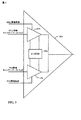
図4は、小さい内側のインダクタがより大きいインダクタからタップされる、タップ付き構成を実装するインダクタ回路30の回路レイアウト・ブロック図である。インダクタ回路30は、それが端子31および32から接地端子35までの1つの大きいコイルを使用するので、ここに記述される他のインダクタ回路よりも望ましくない。小さい方のインダクタは、中間の位置で、すなわち、端子33および34によって、大きいインダクタにタッピングすることにより形成される、しかしながら、小さいインダクタは、端子33および34のけるこれらの中間タップを越えて延長し、インダクタ回路30の性能を実質的に低下させる可能性のある実質的なな寄生容量効果および干渉を付加する。さらに、小さいほうのインダクタは、大きいほうのインダクタからタップされているので、インダクタ回路30の異なるインダクタは通常同じ共振周波数を有する。図5および6に示されるインダクタ設計は、図4のインダクタ回路30のこれらまたは他の欠点を克服できる。インダクタ回路30の例示的な寸方が表示されている。
FIG. 4 is a circuit layout block diagram of an
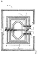
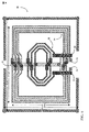
図5および6は、この開示の実例によってより大きいインダクタ内に独立に配置されたインダクタを備えるデユアルインダクタ回路40および50の例示的な回路レイアウト・ブロック図である。デユアルインダクタ回路40および50は、図1および2のインダクタ回路16または25のどちらかに対応してもよいか、あるいは他のタイプの装置で使用されてもよい。コイルが独立しているので、デユアルインダクタ回路40および50の異なるインダクタの共振周波数は、異なって定義することができる。これは高度に望ましい。
5 and 6 are exemplary circuit layout block diagrams of
特に、タップ付きインダクタ設計とは対照的に、図5および6に示されるインダクタ内インダクタ・トポロジー(inductor-inside-inductor topology)は、各独立インタクタ・コイルに対して1つずつ、2つの独立した自己共振周波数を有しうる。外側のインダクタ・コイルは、内側のインダクタ・コイルより低い自己共振周波数を有することができ、また、いくつかの適用に対しては、この共振周波数は、内側のインダクタ・コイルの希望の動作周波数に接近することができる。そのような状況では、内側のインダクタ・コイルを使用する回路の性能への影響は、2つの異なるインダクタ・コイル間の隔離により最小限に抑えることができる。したがって、内側および外側のコイルの両方の間の低い結合により、2つの別個の自己共振周波数が存在することができ、これが、インダクタ内インダクタをより望ましくし、そして、内側のインダクタ・コイルの性能に対する負の影響を小さくすることができる。 In particular, in contrast to the tapped inductor design, the inductor-inside-inductor topology shown in FIGS. 5 and 6 is two independent, one for each independent inductor coil. It can have a self-resonant frequency. The outer inductor coil can have a lower self-resonant frequency than the inner inductor coil, and for some applications, this resonant frequency can be at the desired operating frequency of the inner inductor coil. Can approach. In such situations, the impact on the performance of the circuit using the inner inductor coil can be minimized by the isolation between the two different inductor coils. Thus, due to the low coupling between both the inner and outer coils, there can be two separate self-resonant frequencies, which makes the inductor in the inductor more desirable and does not affect the performance of the inner inductor coil. Negative effects can be reduced.
図5に示されるように、デユアルインダクタ回路40は、第1のインダクタ46および第2のインダクタ48を備える。第2のインダクタ48は、第1のインダクタ46の内側に配置される。両方のインダクタ46および48は、二次元の様式で巻回するコイルを備える。このようにして、回路40は、小さいインダクタ・コイル(第2のインダクタ48)が大きいインダクタ・コイル(第1のインダクタ46)内に配置されるインダクタ内インダクタ設計を定義する。例示の目的のために、デユアルインダクタ回路40の寸法が図5に示されている。しかし、この開示の例は、図5に示されたコイルの寸法または形状に必ずしも限定されない。
As shown in FIG. 5, the
第1のインダクタ46は第1の端子41および第2の端子42を定義する。第1のインダクタ46は、第1および第2の端子41および42から接地端子45までコイル状をなしている。第2のインダクタ48は、第1のインダクタ46の内側に配置されているが、第1のインダクタ46から独立しており、第1のインダクタ46からタップされていない。このように、デユアルインダクタ回路40は、タップ付き構成を使用する図4のインダクタ回路30とは異なっている。デユアルインダクタ回路40では、第2のインダクタ48は、第3の端子43および第4の端子44を定義する。第2のインダクタ48は、第3および第4の端子43および44から接地端子45へのコイル状をなしている。しかし、ここでも、第2のインダクタ48の第3および第4の端子43および44は、第1のインダクタ46からタップされていない限りでは、第1のインダクタ46から独立している。第1のインダクタ46および第2のインダクタ48は、異なる共振周波数を定義するように形成することができる。
The
デユアルインダクタ回路40は、ミキサーが2つの異なる周波数帯を扱うことを可能にするためにミキサーの増幅器内に含まれていてもよい。第1のインダクタ46は、第1の周波数帯の利得を設定してもよく、また、第2のインダクタ48は、第2の周波数帯の利得を設定してもよい。さらに、テストとシミュレーションを使用して、第1のインダクタ46は第2のインダクタ48の寄生効果を減殺するように同調でき、また、第2のインダクタ48は第1のインダクタ46の寄生効果を減殺するように同調できる。第1および第2インダクタ46および48は離隔されているので(互いからタップされていない)、図4に示されたようなタップ付き構成と対比して、これらの寄生効果およびフィード・バックが著しく軽減される。
The
第1のインダクタ46は、無線通信装置の第1の動作モードで使用されてもよく、そして、第2のインダクタ48は、無線通信装置の第2の動作モードで使用されてもよい。第1の動作モードは、約1.0ギガヘルツ(GHz)より低い第1の周波数帯に関連してもよく、また、第2のモードは、約1.0GHzより高い第2の周波数帯に関連してもよい。例示として、第1の周波数帯は約800メガヘルツ(MHz)のまわりのレガシーアナログ帯域でああてもよく、また、第2の周波数帯は約2.4GHzあるいは1.8GHzのまわりの帯域であってもよい。しかし、より一般的には、デユアルインダクタ回路40は、任意の2つの周波数帯に対して同調されうる。
The
図6は、この開示によるデユアルインダクタ回路50の他の実例となる例を提供する回路レイアウト・ブロック図である。デユアルインダクタ回路50は、第1のインダクタ56および第2のインダクタ58を備える。両方のインダクタ56および58は、二次元の様式で巻回するコイルを備える。第2のインダクタ58の二次元のレイアウトは、第1のインダクタ56の二次元のレイアウトの内側に配置される。デユアルインダクタ回路50の寸法が図6に示されている。しかし、この開示の例は、図6に示されているコイルの寸法または形状に必ずしも限定されない。
FIG. 6 is a circuit layout block diagram providing another illustrative example of a
多くの点で、図6のデユアルインダクタ回路50は図5のデユアルインダクタ回路40に類似している。特に、デユアルインダクタ回路50では、第1のインダクタ56は、第1の端子51および第2の端子52を定義し、また、第1のインダクタ56は、第1および第2の端子51および52から接地端子55までコイル状をなしている。第2のインダクタ58は、第1のインダクタ56の内側に配置されるが、第1のインダクタ56から独立おり、第1のインダクタ56からタップされていない。このように、デユアルインダクタ回路50は、デユアルインダクタ回路40と同様に、タップ付き構成を定義する図4のインダクタ回路30とは異なる。
In many respects, the
デユアルインダクタ回路50では、第2のインダクタ58は第3の端子53および第4の端子54を定義する。第2のインダクタ58は、第3および第4の端子53および54から接地端子55までコイル状をなしている。
In the
第2のインダクタ58の第3および第4の端子53および54は、第1のインダクタ56からタップされていない限りにおいて、最初のインダクタ56から独立している。これはまた、第1のインダクタ56および第2のインダクタ58が異なる共振周波数を定義するように作成されることを可能にしており、これは非常に望ましい。
The third and
デユアルインダクタ回路50は、ミキサーが2つの異なる周波数帯を扱うことを可能にするためにミキサーの増幅器内に含まれていてもよい。第1のインダクタ56は第1の周波数帯に同調されてもよく、また、第2のインダクタ58は第2の周波数帯に同調されてもよい。さらに、シミュレーションとテストを使用して、第1のインダクタ56は、第2のインダクタ58の寄生効果を減殺するように同調することができ、また、第2のインダクタ58は、第1のインダクタ56の寄生効果を減殺するように同調することができる。
A
デユアルインダクタ回路50は、デユアルインダクタ回路40の第1のインダクタ46と第2のインダクタ48の間のそれと比較して第1のインダクタ56と第2のインダクタ58の間の物理的離隔が大きいので、デユアルインダクタ回路40に対比して寄生効果をさらに低減させる。特に、第2のインダクタ58は、約20ミクロンより大きく第1のインダクタ56から離隔されてもよい。これは、インダクタ56と58の間の電磁妨害および寄生効果をさらに低減または除去するのを助けることができる。デユアルインダクタ回路50に関連した表面積は約0.3平方ミリメートル未満を定義するが、この開示は必ずしもこの点では限定されない。
Since the
第1および第2インダクタ56および58は、20ミクロンより大きいスペースによって分離されただけでなく、隔離されている(互いにタップされていない)。上述のように、この隔離はまた、インダクタ56と58の間の寄生効果および電磁結合効果を低減するのに非常に有用である。特に、インダクタ56および58の物理的な隔離は、タップ付き構成とは対照的に、インダクタ56と58の間の寄生容量および電磁結合を著しく低減することができる。さらに、この隔離は、インダクタに56と58が異なる共振周波数を定義することを可能にし、これは、異なるインダクタによって扱われる異なる周波数帯に対する性能の影響をを回避することができる。 The first and second inductors 56 and 58 are not only separated by a space greater than 20 microns, but are also isolated (not tapped from each other). As mentioned above, this isolation is also very useful in reducing parasitic and electromagnetic coupling effects between inductors 56 and 58. In particular, the physical isolation of inductors 56 and 58 can significantly reduce parasitic capacitance and electromagnetic coupling between inductors 56 and 58, as opposed to a tapped configuration. Furthermore, this isolation allows the inductors 56 and 58 to define different resonant frequencies, which can avoid performance impacts on different frequency bands handled by different inductors.
第1のインダクタ56は、無線通信装置の第1の動作モードで使用されてもよく、また、第2のインダクタ58は、無線通信装置の第2の動作モードで使用されてもよい。第1の動作モードは、約1.0GHz未満の第1の周波数帯に関連されてもよく、また、第2のモードは、約1.0GHzより高い第2の周波数帯に関連されてもよい。例示の実例として、第1の周波数帯は約800メガヘルツ(MHz)のまわりのレガシーアナログ帯域であってもよく、また、第2の周波数帯は約2.4GHzあるいは1.8GHzのまわりのPCS帯域であってもよい。しかし、より一般的には、デユアルインダクタ回路50は、任意の2つの周波数帯に対してを同調することができるかもしれない。1つの例として、第1のインダクタ56は、約0.35〜0.6ミリメートルの距離にわたって巻回してもよく、また、第2のインダクタ58は、約0.2〜0.32ミリメートルの距離にわたって巻回してもよい。
The first inductor 56 may be used in a first operation mode of the wireless communication device, and the second inductor 58 may be used in a second operation mode of the wireless communication device. The first mode of operation may be associated with a first frequency band less than about 1.0 GHz, and the second mode may be associated with a second frequency band higher than about 1.0 GHz. As an illustrative example, the first frequency band may be a legacy analog band around about 800 megahertz (MHz), and the second frequency band is a PCS band around 2.4 GHz or 1.8 GHz. May be. More generally, however, the
ここに記述されるようなデユアルインダクタ回路を実装する無線通信装置によって実行されてもよい方法を例証する流れ図である。図7の機能性は、図1の無線通信装置10に関して記述されるであろう。図7に示されるように、装置10は、1.0GHzより高い周波数帯で動作するデジタルPCSモード、あるいは1.0GHz未満の周波数帯で動作するアナログ(あるいは他のモード) のような動作モードを選択する(61)。アンテナ12は、搬送波上に変調されたベースバンド信号を含む無線信号を受信する(62)。動作モードに依存して(63)、ミキサー15のインダクタ回路16は第1の(外側の)コイルあるいは第2の(内側の)コイルのいずれかを選択する。
6 is a flow diagram illustrating a method that may be performed by a wireless communication device that implements a dual inductor circuit as described herein. The functionality of FIG. 7 will be described with respect to the wireless communication device 10 of FIG. As shown in FIG. 7, the device 10 selects an operating mode such as a digital PCS mode operating in a frequency band higher than 1.0 GHz, or an analog (or other mode) operating in a frequency band lower than 1.0 GHz (61). The
特に、LNAs 14Aまたは14Bのうちの1つによってスケールすることに従って、受信信号は、ミキサー15に渡される。装置10が第1の動作モード(63の"ONE"ブランチ)で作動している場合には、ミキサー15は混合処理でインダクタ回路16の第1のインダクタを使用する(64)。あるいは、装置10が第2の動作モード(63の" TWO "ブランチ)で動作している場合には、ミキサー15は混合処理でインダクタ回路16の第2のインダクタを使用する(65)。ここに記述されるように、第2のインダクタは第1のインダクタ内に配置されるが、第1のインダクタからタップされていない独立した端子を含んでいる。接地端子は第1および第2のインダクタによって共有されてもよい。このようにして、ミキサー15は、2つの異なる周波数帯に関連した受信信号に対するベースバンド信号を生成することができる。
In particular, the received signal is passed to the
ベースバンド信号はA/Dコンバータ18によってデジタル・サンプルに変換することができ(66)、また、デジタル復調回路19はデジタル・ベースバンド・サンプルに関して復調を行なうことができる(67)。もちろん、この開示の技術は、デジタル・サンプルに変換されないであろう純粋にアナログの信号に対しても実行できるが、アナログ・ドメインで復調されるであろう。言いかえれば、装置10の動作モードの1つ又は両方は純粋にアナログのモードでありうる。
The baseband signal can be converted to digital samples by the A / D converter 18 (66), and the
多くの実例が記述された。開示されたインダクタ内側インダクタは、高周波集積回路(RFIC)上に製作することができ、そのようなRFIC製作に関連する必要な面積およびコストを低減することができる。RFICチップ上のミキサーに関して記述されたが、開示されたデユアルインダクタ回路は他の装置で使用することもできるであろう。さらに、開示されたインダクタは、キャリア上にベースバンド信号を混合するRF発信機のミキサーで使用することもできるであろう。従って、これらおよび他の例は下記の請求項の範囲内である。 Many examples have been described. The disclosed inductor inner inductor can be fabricated on a radio frequency integrated circuit (RFIC) and can reduce the required area and cost associated with such RFIC fabrication. Although described with respect to a mixer on an RFIC chip, the disclosed dual inductor circuit could also be used in other devices. Furthermore, the disclosed inductor could be used in an RF transmitter mixer that mixes a baseband signal on a carrier. Accordingly, these and other examples are within the scope of the following claims.
本出願は、2006年7月28日に申請されて、米国仮出願数60/834,129の利益を請求する、その全内容は、基準によってここに組込まれる。 This application was filed on July 28, 2006 and claims the benefit of US provisional application number 60 / 834,129, the entire contents of which are hereby incorporated by reference.
Claims (30)
第1の端子および第2の端子を定義し、前記第1および第2端子から接地端子までコイル状をなす第1のインダクタと、
前記第1のインダクタの内側に配置され、第3の端子および第4の端子を定義し、該第3および第4の端子から接地端子までコイル状をなし、前記第3および第4の端子は前記第1のインダクタから独立である第2のインダクタと、
を含み、
前記第1のインダクタは、前記ミキサーが前記第1の周波数帯域をサポートするように前記装置の前記第1の動作モードで使用され、前記第2のインダクタは、前記ミキサーが前記第2の周波数帯域をサポートするように前記装置の前記第2の動作モードで使用される、多帯域無線通信装置。A multi-band wireless communication apparatus having a first operation mode associated with a first frequency band and a second operation mode associated with a second frequency band different from the first frequency band, from a received signal A single mixer for generating a baseband signal, the mixer comprising a dual inductor circuit, the dual inductor circuit comprising:
A first inductor defining a first terminal and a second terminal and coiled from the first and second terminals to the ground terminal;
It is arranged inside the first inductor, defines a third terminal and a fourth terminal, is coiled from the third and fourth terminals to the ground terminal, and the third and fourth terminals are A second inductor that is independent of the first inductor;
Only including,
The first inductor is used in the first mode of operation of the apparatus such that the mixer supports the first frequency band, and the second inductor is used by the mixer in the second frequency band. A multi-band wireless communication device used in the second mode of operation of the device to support
前記ベースバンド信号をデジタル・ベースバンド・サンプルに変換するアナログ・デジタル変換器と、
前記デジタル・ベースバンド・サンプルを復調するデジタル復調回路と、
をさらに備える、請求項1の多帯域無線通信装置。The mixer generates a baseband signal, and the multiband wireless communication device
An analog-to-digital converter that converts the baseband signal to digital baseband samples;
A digital demodulation circuit for demodulating the digital baseband samples;
The multiband wireless communication apparatus according to claim 1, further comprising:
第1の端子および第2の端子を定義し、前記第1および第2の端子から接地端子までコイル状をなす第1のインダクタと、
前記第1のインダクタの内側に配置され、第3の端子および第4の端子を定義し、前記第3および第4の端子から接地端子までコイル状をなし、前記第3および第4の端子は前記第1のインダクタから独立である第2のインダクタと、
を備え、
前記第1のインダクタは、前記ミキサーが前記第1の周波数帯域をサポートするように前記装置の前記第1の動作モードで使用され、前記第2のインダクタは、前記ミキサーが前記第2の周波数帯域をサポートするように前記装置の前記第2の動作モードで使用される、デユアルインダクタ回路。A single mixer provided in a multi-band wireless communication having a first operation mode associated with a first frequency band and a second operation mode associated with a second frequency band different from the first frequency band A dual inductor circuit for
A first inductor defining a first terminal and a second terminal and having a coil shape from the first and second terminals to the ground terminal;
It is arranged inside the first inductor, defines a third terminal and a fourth terminal, has a coil shape from the third and fourth terminals to the ground terminal, and the third and fourth terminals are A second inductor that is independent of the first inductor;
With
The first inductor is used in the first mode of operation of the apparatus such that the mixer supports the first frequency band, and the second inductor is used by the mixer in the second frequency band. A dual inductor circuit used in the second mode of operation of the device to support
第1の端子および第2の端子を定義し、前記第1および第2の端子から接地端子までコイル状をなす第1のインダクタと、
前記第1のインダクタの内側に配置され、第3の端子および第4の端子を定義し、前記第3および第4の端子から前記接地端子までコイル状をなし、前記第3および第4の端子は前記第1のインダクタから独立である第2のインダクタと、を含み、
前記第1のインダクタは、前記単一のミキサーが前記第1の周波数帯域をサポートするように前記装置の前記第1の動作モードで使用され、前記第2のインダクタは、前記ミキサーが前記第2の周波数帯域をサポートするように前記装置の前記第2の動作モードで使用される、方法。A selected inductor of a dual inductor circuit in a wireless communication device having a first operating mode associated with a first frequency band and a second operating mode associated with a second frequency band different from the first frequency band Using a single mixer to mix a received radio signal into a baseband signal, the dual inductor circuit comprising:
A first inductor defining a first terminal and a second terminal and having a coil shape from the first and second terminals to the ground terminal;
The third inductor is disposed inside the first inductor, defines a third terminal and a fourth terminal, has a coil shape from the third and fourth terminals to the ground terminal, and the third and fourth terminals see containing the second inductor is independent from said first inductor, and
The first inductor is used in the first mode of operation of the device such that the single mixer supports the first frequency band, and the second inductor is used by the mixer in the second mode. Used in the second mode of operation of the apparatus to support a frequency band of.
および前記デジタル・ベースバンド・サンプルを復調すること、をさらに備える、請求項19の方法。Converting the baseband signal into digital baseband samples;
20. The method of claim 19, further comprising: demodulating the digital baseband samples.
第1の端子および第2の端子を定義し、前記第1および第2の端子から接地端子までコイル状をなす第1のインダクタと、
前記第1のインダクタの内側に配置され、第3の端子および第4の端子を定義し、前記第3および第4の端子から前記接地端子までコイル状をなし、前記第3および第4の端子は前記第1のインダクタから独立である第2のインダクタと、を含むデュアルインダクタ回路を備え、
前記第1のインダクタは、前記ミキサーが前記第1の周波数帯域をサポートするように前記装置の前記第1の動作モードで使用され、前記第2のインダクタは、前記単一のミキサーが前記第2の周波数帯域をサポートするように前記装置の前記第2の動作モードで使用される、多帯域無線通信装置。A multiband wireless communication apparatus having a first operation mode associated with a first frequency band and a second operation mode associated with a second frequency band different from the first frequency band, the carrier comprising: A single mixer for mixing the baseband signal, the single mixer
A first inductor defining a first terminal and a second terminal and having a coil shape from the first and second terminals to the ground terminal;
The third and fourth terminals are arranged inside the first inductor, define a third terminal and a fourth terminal, form a coil from the third and fourth terminals to the ground terminal, and Comprises a dual inductor circuit including a second inductor that is independent of the first inductor;
The first inductor is used in the first mode of operation of the apparatus such that the mixer supports the first frequency band, and the second inductor is used by the single mixer to the second A multi-band wireless communication device used in the second mode of operation of the device to support multiple frequency bands.
Applications Claiming Priority (5)
| Application Number | Priority Date | Filing Date | Title |
|---|---|---|---|
| US83412906P | 2006-07-28 | 2006-07-28 | |
| US60/834,129 | 2006-07-28 | ||
| US11/675,274 | 2007-02-15 | ||
| US11/675,274 US7761078B2 (en) | 2006-07-28 | 2007-02-15 | Dual inductor circuit for multi-band wireless communication device |
| PCT/US2007/074718 WO2008014506A2 (en) | 2006-07-28 | 2007-07-30 | Dual inductor circuit for multi-band wireless communication device |
Related Child Applications (1)
| Application Number | Title | Priority Date | Filing Date |
|---|---|---|---|
| JP2011128130A Division JP2011250418A (en) | 2006-07-28 | 2011-06-08 | Multi-band purpose dual inductor circuit |
Publications (2)
| Publication Number | Publication Date |
|---|---|
| JP2009545278A JP2009545278A (en) | 2009-12-17 |
| JP4851592B2 true JP4851592B2 (en) | 2012-01-11 |
Family
ID=38769914
Family Applications (2)
| Application Number | Title | Priority Date | Filing Date |
|---|---|---|---|
| JP2009522988A Expired - Fee Related JP4851592B2 (en) | 2006-07-28 | 2007-07-30 | Dual inductor circuit for multi-band |
| JP2011128130A Pending JP2011250418A (en) | 2006-07-28 | 2011-06-08 | Multi-band purpose dual inductor circuit |
Family Applications After (1)
| Application Number | Title | Priority Date | Filing Date |
|---|---|---|---|
| JP2011128130A Pending JP2011250418A (en) | 2006-07-28 | 2011-06-08 | Multi-band purpose dual inductor circuit |
Country Status (7)
| Country | Link |
|---|---|
| US (2) | US7761078B2 (en) |
| EP (1) | EP2047606B1 (en) |
| JP (2) | JP4851592B2 (en) |
| KR (1) | KR101109374B1 (en) |
| CN (1) | CN101496294B (en) |
| TW (1) | TW200828828A (en) |
| WO (1) | WO2008014506A2 (en) |
Families Citing this family (28)
| Publication number | Priority date | Publication date | Assignee | Title |
|---|---|---|---|---|
| US8219060B2 (en) | 2006-07-28 | 2012-07-10 | Qualcomm Incorporated | Dual inductor circuit for multi-band wireless communication device |
| US8063769B2 (en) * | 2007-03-30 | 2011-11-22 | Broadcom Corporation | Dual band antenna and methods for use therewith |
| US7952528B2 (en) * | 2007-09-04 | 2011-05-31 | Sierra Wireless, Inc. | Antenna configurations for compact device wireless communication |
| US20090124215A1 (en) * | 2007-09-04 | 2009-05-14 | Sierra Wireless, Inc. | Antenna Configurations for Compact Device Wireless Communication |
| US8049671B2 (en) | 2007-09-04 | 2011-11-01 | Sierra Wireless, Inc. | Antenna configurations for compact device wireless communication |
| US20090122847A1 (en) * | 2007-09-04 | 2009-05-14 | Sierra Wireless, Inc. | Antenna Configurations for Compact Device Wireless Communication |
| US8059046B2 (en) * | 2007-09-04 | 2011-11-15 | Sierra Wireless, Inc. | Antenna configurations for compact device wireless communication |
| US7916090B2 (en) * | 2007-09-04 | 2011-03-29 | Sierra Wireless, Inc. | Antenna configurations for compact device wireless communication |
| JP2009194302A (en) * | 2008-02-18 | 2009-08-27 | Mitsubishi Electric Corp | Semiconductor integrated circuit |
| US7834712B2 (en) * | 2008-10-09 | 2010-11-16 | Altera Corporation | Techniques for providing option conductors to connect components in an oscillator circuit |
| US9111675B1 (en) | 2010-04-07 | 2015-08-18 | Xilinx, Inc. | Stacked inductor structure |
| US8143987B2 (en) * | 2010-04-07 | 2012-03-27 | Xilinx, Inc. | Stacked dual inductor structure |
| US20120244802A1 (en) * | 2011-03-24 | 2012-09-27 | Lei Feng | On chip inductor |
| US8717723B2 (en) | 2012-01-10 | 2014-05-06 | Xilinx, Inc. | Driver circuit and method of generating an output signal |
| US8989691B2 (en) | 2012-04-19 | 2015-03-24 | Qualcomm Incorporated | Impedance balancing for power supply rejection in single-ended receivers |
| CN103400820B (en) * | 2013-01-30 | 2016-08-10 | 威盛电子股份有限公司 | Semiconductor device |
| US9048017B2 (en) | 2013-03-14 | 2015-06-02 | Xilinx, Inc. | Circuits for and methods of implementing a gain stage in an integrated circuit |
| US20160170983A1 (en) * | 2013-07-30 | 2016-06-16 | Nippon Telegraph And Telephone Corporation | Information management apparatus and information management method |
| DE102013111433A1 (en) * | 2013-08-30 | 2015-03-05 | Technische Universität Dresden | Planar balanced coil for integrated RF circuits |
| US9543068B2 (en) * | 2014-06-17 | 2017-01-10 | Qualcomm Technologies International, Ltd. | Inductor structure and application thereof |
| EP2963646A1 (en) * | 2014-07-01 | 2016-01-06 | Fraunhofer-Gesellschaft zur Förderung der angewandten Forschung e.V. | Decoder and method for decoding an audio signal, encoder and method for encoding an audio signal |
| TW201604902A (en) | 2014-07-30 | 2016-02-01 | 瑞昱半導體股份有限公司 | Integral inductor structure |
| CN105448885A (en) * | 2014-08-06 | 2016-03-30 | 瑞昱半导体股份有限公司 | Integrated Inductor Structure |
| US9922763B2 (en) * | 2014-10-28 | 2018-03-20 | Mediatek Singapore Pte. Ltd. | Transformer with two transformation ratio |
| US20160125995A1 (en) * | 2014-10-31 | 2016-05-05 | Qualcomm Incorporated | Array of interleaved 8-shaped transformers with high isolation between adjacent elements |
| KR102492575B1 (en) * | 2015-02-05 | 2023-01-30 | 삼성전자주식회사 | Inductor device |
| WO2017205176A1 (en) * | 2016-05-23 | 2017-11-30 | X-Card Holdings, Llc | Multiple interface electronic card |
| US11139779B2 (en) * | 2019-10-21 | 2021-10-05 | Samsung Electronics Co., Ltd. | Dual band mixer |
Family Cites Families (21)
| Publication number | Priority date | Publication date | Assignee | Title |
|---|---|---|---|---|
| CN1093705C (en) * | 1998-02-18 | 2002-10-30 | 摩托罗拉公司 | Method and apparatus for receiving communication signals |
| WO2001093422A1 (en) * | 2000-06-01 | 2001-12-06 | Koninklijke Philips Electronics N.V. | Rf circuit |
| FR2812445B1 (en) | 2000-07-31 | 2002-11-29 | St Microelectronics Sa | INTEGRATED STRUCTURE OF SHARED VALUE INDUCTANCES ON A SEMICONDUCTOR SUBSTRATE |
| EP1261033B1 (en) * | 2001-05-24 | 2006-08-30 | Nokia Corporation | On chip inductive structure |
| JP2003045722A (en) * | 2001-08-01 | 2003-02-14 | Sony Corp | Inductor element and integrated circuit using inductor element |
| US6975841B2 (en) * | 2001-11-12 | 2005-12-13 | Matsushita Electric Industrial Co., Ltd. | Diplexer, and high-frequency switch and antenna duplexer using the same |
| DE10162263A1 (en) | 2001-12-18 | 2003-07-10 | Infineon Technologies Ag | Inductive component |
| KR20030056243A (en) * | 2001-12-27 | 2003-07-04 | 삼성전기주식회사 | Triplexer circuit and chip multilayer triplexer |
| JP2003264348A (en) | 2002-03-07 | 2003-09-19 | Sony Corp | High frequency module |
| US6751470B1 (en) * | 2002-04-08 | 2004-06-15 | Nokia Corporation | Versatile RF front-end multiband mobile terminals |
| US6707367B2 (en) * | 2002-07-23 | 2004-03-16 | Broadcom, Corp. | On-chip multiple tap transformer and inductor |
| FR2851078A1 (en) | 2003-02-07 | 2004-08-13 | St Microelectronics Sa | INTEGRATED INDUCTANCE AND ELECTRONIC CIRCUIT INCORPORATING THE SAME |
| JP4383259B2 (en) * | 2003-08-20 | 2009-12-16 | シャープ株式会社 | Frequency converter and wireless communication device using the same |
| US6972658B1 (en) | 2003-11-10 | 2005-12-06 | Rf Micro Devices, Inc. | Differential inductor design for high self-resonance frequency |
| TWI263397B (en) * | 2004-01-20 | 2006-10-01 | Delta Electronics Inc | Single stage A/D converter with piezo transformer |
| JP4391263B2 (en) | 2004-02-20 | 2009-12-24 | Okiセミコンダクタ株式会社 | Semiconductor device, method for manufacturing the same, and high-frequency integrated circuit using the semiconductor device |
| US7242274B2 (en) | 2004-03-03 | 2007-07-10 | Atheros Communications, Inc. | Inductor layout using step symmetry for inductors |
| JP2005303839A (en) * | 2004-04-14 | 2005-10-27 | Matsushita Electric Ind Co Ltd | Voltage controlled oscillator |
| US7262681B2 (en) * | 2005-02-11 | 2007-08-28 | Semiconductor Components Industries, L.L.C. | Integrated semiconductor inductor and method therefor |
| KR100698617B1 (en) * | 2005-02-15 | 2007-03-21 | 삼성전자주식회사 | Integrated Circuits with Integrated Inductors |
| FI20055402A0 (en) | 2005-07-11 | 2005-07-11 | Nokia Corp | Inductor for multi-band radio frequency operation |
-
2007
- 2007-02-15 US US11/675,274 patent/US7761078B2/en not_active Expired - Fee Related
- 2007-07-30 KR KR1020097004433A patent/KR101109374B1/en not_active Expired - Fee Related
- 2007-07-30 WO PCT/US2007/074718 patent/WO2008014506A2/en not_active Ceased
- 2007-07-30 EP EP07840583.4A patent/EP2047606B1/en not_active Not-in-force
- 2007-07-30 CN CN2007800277309A patent/CN101496294B/en not_active Expired - Fee Related
- 2007-07-30 TW TW096127857A patent/TW200828828A/en unknown
- 2007-07-30 JP JP2009522988A patent/JP4851592B2/en not_active Expired - Fee Related
-
2010
- 2010-06-29 US US12/826,552 patent/US8229385B2/en not_active Expired - Fee Related
-
2011
- 2011-06-08 JP JP2011128130A patent/JP2011250418A/en active Pending
Also Published As
| Publication number | Publication date |
|---|---|
| WO2008014506A3 (en) | 2008-03-13 |
| WO2008014506A2 (en) | 2008-01-31 |
| CN101496294A (en) | 2009-07-29 |
| JP2009545278A (en) | 2009-12-17 |
| TW200828828A (en) | 2008-07-01 |
| JP2011250418A (en) | 2011-12-08 |
| US20080024349A1 (en) | 2008-01-31 |
| EP2047606A2 (en) | 2009-04-15 |
| US20100265022A1 (en) | 2010-10-21 |
| CN101496294B (en) | 2013-04-24 |
| KR20090046914A (en) | 2009-05-11 |
| US7761078B2 (en) | 2010-07-20 |
| EP2047606B1 (en) | 2015-12-23 |
| KR101109374B1 (en) | 2012-01-30 |
| US8229385B2 (en) | 2012-07-24 |
Similar Documents
| Publication | Publication Date | Title |
|---|---|---|
| JP4851592B2 (en) | Dual inductor circuit for multi-band | |
| US8331978B2 (en) | Dual inductor circuit for multi-band wireless communication device | |
| US8559186B2 (en) | Inductor with patterned ground plane | |
| JP6279556B2 (en) | Low noise amplifier for carrier aggregation with transformer-based signal division | |
| EP2920879B1 (en) | Omni-band amplifiers | |
| US20200106403A1 (en) | Radio frequency amplifiers with an injection-locked oscillator driver stage and a stacked output stage | |
| KR101793148B1 (en) | Multi-band power amplifier | |
| US20130285198A1 (en) | Semiconductor device | |
| WO2016039923A1 (en) | Dual-band low noise amplifier | |
| CN104079311A (en) | Communication system and communication control method | |
| US20200106398A1 (en) | Transformer Reconfigurability for Wireless Transceivers | |
| HK1133961A (en) | Dual inductor circuit for multi-band wireless communication device | |
| US10832848B2 (en) | Low DC resistance and high RF resistance power amplifier choke inductor | |
| US20240429587A1 (en) | Low emission three-dimensional frequency multiplexer | |
| CN121727512A (en) | Multipath amplifier circuit with compact transformer | |
| WO2025064109A1 (en) | Pseudo bi-directional amplifier | |
| CN121602931A (en) | Harmonic conversion gain reduction for mixer circuits | |
| CN121603032A (en) | Harmonic leakage suppression for wireless circuits | |
| Hussaini et al. | Green Multi-homing RF Architectures |
Legal Events
| Date | Code | Title | Description |
|---|---|---|---|
| A131 | Notification of reasons for refusal |
Free format text: JAPANESE INTERMEDIATE CODE: A131 Effective date: 20100817 |
|
| A521 | Request for written amendment filed |
Free format text: JAPANESE INTERMEDIATE CODE: A523 Effective date: 20101112 |
|
| A02 | Decision of refusal |
Free format text: JAPANESE INTERMEDIATE CODE: A02 Effective date: 20110208 |
|
| A521 | Request for written amendment filed |
Free format text: JAPANESE INTERMEDIATE CODE: A523 Effective date: 20110608 |
|
| A911 | Transfer to examiner for re-examination before appeal (zenchi) |
Free format text: JAPANESE INTERMEDIATE CODE: A911 Effective date: 20110616 |
|
| A131 | Notification of reasons for refusal |
Free format text: JAPANESE INTERMEDIATE CODE: A131 Effective date: 20110809 |
|
| A521 | Request for written amendment filed |
Free format text: JAPANESE INTERMEDIATE CODE: A523 Effective date: 20110824 |
|
| TRDD | Decision of grant or rejection written | ||
| A01 | Written decision to grant a patent or to grant a registration (utility model) |
Free format text: JAPANESE INTERMEDIATE CODE: A01 Effective date: 20110920 |
|
| A01 | Written decision to grant a patent or to grant a registration (utility model) |
Free format text: JAPANESE INTERMEDIATE CODE: A01 |
|
| A61 | First payment of annual fees (during grant procedure) |
Free format text: JAPANESE INTERMEDIATE CODE: A61 Effective date: 20111020 |
|
| R150 | Certificate of patent or registration of utility model |
Free format text: JAPANESE INTERMEDIATE CODE: R150 |
|
| FPAY | Renewal fee payment (event date is renewal date of database) |
Free format text: PAYMENT UNTIL: 20141028 Year of fee payment: 3 |
|
| R250 | Receipt of annual fees |
Free format text: JAPANESE INTERMEDIATE CODE: R250 |
|
| R250 | Receipt of annual fees |
Free format text: JAPANESE INTERMEDIATE CODE: R250 |
|
| R250 | Receipt of annual fees |
Free format text: JAPANESE INTERMEDIATE CODE: R250 |
|
| R250 | Receipt of annual fees |
Free format text: JAPANESE INTERMEDIATE CODE: R250 |
|
| LAPS | Cancellation because of no payment of annual fees |