JP4398225B2 - Semiconductor device - Google Patents
Semiconductor device Download PDFInfo
- Publication number
- JP4398225B2 JP4398225B2 JP2003376415A JP2003376415A JP4398225B2 JP 4398225 B2 JP4398225 B2 JP 4398225B2 JP 2003376415 A JP2003376415 A JP 2003376415A JP 2003376415 A JP2003376415 A JP 2003376415A JP 4398225 B2 JP4398225 B2 JP 4398225B2
- Authority
- JP
- Japan
- Prior art keywords
- chip
- main surface
- electrodes
- wiring
- semiconductor device
- Prior art date
- Legal status (The legal status is an assumption and is not a legal conclusion. Google has not performed a legal analysis and makes no representation as to the accuracy of the status listed.)
- Expired - Fee Related
Links
Images


Classifications
-
- H—ELECTRICITY
- H10—SEMICONDUCTOR DEVICES; ELECTRIC SOLID-STATE DEVICES NOT OTHERWISE PROVIDED FOR
- H10W—GENERIC PACKAGES, INTERCONNECTIONS, CONNECTORS OR OTHER CONSTRUCTIONAL DETAILS OF DEVICES COVERED BY CLASS H10
- H10W72/00—Interconnections or connectors in packages
- H10W72/50—Bond wires
- H10W72/531—Shapes of wire connectors
- H10W72/536—Shapes of wire connectors the connected ends being ball-shaped
-
- H—ELECTRICITY
- H10—SEMICONDUCTOR DEVICES; ELECTRIC SOLID-STATE DEVICES NOT OTHERWISE PROVIDED FOR
- H10W—GENERIC PACKAGES, INTERCONNECTIONS, CONNECTORS OR OTHER CONSTRUCTIONAL DETAILS OF DEVICES COVERED BY CLASS H10
- H10W72/00—Interconnections or connectors in packages
- H10W72/50—Bond wires
- H10W72/531—Shapes of wire connectors
- H10W72/5363—Shapes of wire connectors the connected ends being wedge-shaped
-
- H—ELECTRICITY
- H10—SEMICONDUCTOR DEVICES; ELECTRIC SOLID-STATE DEVICES NOT OTHERWISE PROVIDED FOR
- H10W—GENERIC PACKAGES, INTERCONNECTIONS, CONNECTORS OR OTHER CONSTRUCTIONAL DETAILS OF DEVICES COVERED BY CLASS H10
- H10W72/00—Interconnections or connectors in packages
- H10W72/50—Bond wires
- H10W72/551—Materials of bond wires
- H10W72/552—Materials of bond wires comprising metals or metalloids, e.g. silver
- H10W72/5522—Materials of bond wires comprising metals or metalloids, e.g. silver comprising gold [Au]
-
- H—ELECTRICITY
- H10—SEMICONDUCTOR DEVICES; ELECTRIC SOLID-STATE DEVICES NOT OTHERWISE PROVIDED FOR
- H10W—GENERIC PACKAGES, INTERCONNECTIONS, CONNECTORS OR OTHER CONSTRUCTIONAL DETAILS OF DEVICES COVERED BY CLASS H10
- H10W72/00—Interconnections or connectors in packages
- H10W72/851—Dispositions of multiple connectors or interconnections
- H10W72/874—On different surfaces
- H10W72/877—Bump connectors and die-attach connectors
-
- H—ELECTRICITY
- H10—SEMICONDUCTOR DEVICES; ELECTRIC SOLID-STATE DEVICES NOT OTHERWISE PROVIDED FOR
- H10W—GENERIC PACKAGES, INTERCONNECTIONS, CONNECTORS OR OTHER CONSTRUCTIONAL DETAILS OF DEVICES COVERED BY CLASS H10
- H10W72/00—Interconnections or connectors in packages
- H10W72/851—Dispositions of multiple connectors or interconnections
- H10W72/874—On different surfaces
- H10W72/884—Die-attach connectors and bond wires
-
- H—ELECTRICITY
- H10—SEMICONDUCTOR DEVICES; ELECTRIC SOLID-STATE DEVICES NOT OTHERWISE PROVIDED FOR
- H10W—GENERIC PACKAGES, INTERCONNECTIONS, CONNECTORS OR OTHER CONSTRUCTIONAL DETAILS OF DEVICES COVERED BY CLASS H10
- H10W74/00—Encapsulations, e.g. protective coatings
- H10W74/10—Encapsulations, e.g. protective coatings characterised by their shape or disposition
- H10W74/15—Encapsulations, e.g. protective coatings characterised by their shape or disposition on active surfaces of flip-chip devices, e.g. underfills
-
- H—ELECTRICITY
- H10—SEMICONDUCTOR DEVICES; ELECTRIC SOLID-STATE DEVICES NOT OTHERWISE PROVIDED FOR
- H10W—GENERIC PACKAGES, INTERCONNECTIONS, CONNECTORS OR OTHER CONSTRUCTIONAL DETAILS OF DEVICES COVERED BY CLASS H10
- H10W90/00—Package configurations
- H10W90/701—Package configurations characterised by the relative positions of pads or connectors relative to package parts
- H10W90/721—Package configurations characterised by the relative positions of pads or connectors relative to package parts of bump connectors
- H10W90/724—Package configurations characterised by the relative positions of pads or connectors relative to package parts of bump connectors between a chip and a stacked insulating package substrate, interposer or RDL
-
- H—ELECTRICITY
- H10—SEMICONDUCTOR DEVICES; ELECTRIC SOLID-STATE DEVICES NOT OTHERWISE PROVIDED FOR
- H10W—GENERIC PACKAGES, INTERCONNECTIONS, CONNECTORS OR OTHER CONSTRUCTIONAL DETAILS OF DEVICES COVERED BY CLASS H10
- H10W90/00—Package configurations
- H10W90/701—Package configurations characterised by the relative positions of pads or connectors relative to package parts
- H10W90/731—Package configurations characterised by the relative positions of pads or connectors relative to package parts of die-attach connectors
- H10W90/732—Package configurations characterised by the relative positions of pads or connectors relative to package parts of die-attach connectors between stacked chips
-
- H—ELECTRICITY
- H10—SEMICONDUCTOR DEVICES; ELECTRIC SOLID-STATE DEVICES NOT OTHERWISE PROVIDED FOR
- H10W—GENERIC PACKAGES, INTERCONNECTIONS, CONNECTORS OR OTHER CONSTRUCTIONAL DETAILS OF DEVICES COVERED BY CLASS H10
- H10W90/00—Package configurations
- H10W90/701—Package configurations characterised by the relative positions of pads or connectors relative to package parts
- H10W90/731—Package configurations characterised by the relative positions of pads or connectors relative to package parts of die-attach connectors
- H10W90/734—Package configurations characterised by the relative positions of pads or connectors relative to package parts of die-attach connectors between a chip and a stacked insulating package substrate, interposer or RDL
-
- H—ELECTRICITY
- H10—SEMICONDUCTOR DEVICES; ELECTRIC SOLID-STATE DEVICES NOT OTHERWISE PROVIDED FOR
- H10W—GENERIC PACKAGES, INTERCONNECTIONS, CONNECTORS OR OTHER CONSTRUCTIONAL DETAILS OF DEVICES COVERED BY CLASS H10
- H10W90/00—Package configurations
- H10W90/701—Package configurations characterised by the relative positions of pads or connectors relative to package parts
- H10W90/751—Package configurations characterised by the relative positions of pads or connectors relative to package parts of bond wires
- H10W90/754—Package configurations characterised by the relative positions of pads or connectors relative to package parts of bond wires between a chip and a stacked insulating package substrate, interposer or RDL
Landscapes
- Wire Bonding (AREA)
Description
本発明は、半導体装置に関し、特に、複数の半導体チップを有したチップ積層型の半導体装置に適用して有効な技術に関する。 The present invention relates to semiconductor equipment and, more particularly, to a technique effectively applied to a chip-stacked type semiconductor device having a plurality of semiconductor chips.
従来のチップ積層型の半導体装置(マルチチップモジュール)では、そのパッケージ基板の主面上に実装された3個のチップのうち、DRAM(Dynamic Random Access Memory) が形成されたチップおよびフラッシュメモリが形成されたチップは、それぞれAuバンプを介してパッケージ基板の配線と電気的に接続されており、さらに2個のチップの上には高速マイクロプロセッサが形成されたチップが実装され、このチップはAuワイヤを介してパッケージ基板のボンディングパッドと電気的に接続されている(例えば、特許文献1参照)。
配線基板の主面上に半導体チップがフリップチップ接続され、さらにこの半導体チップ上に他の半導体チップが積層され、上段の半導体チップが配線基板に対してワイヤボンディングされる構造の半導体装置(マルチチップモジュールやマルチチップパッケージなど)では、配線基板の主面の周縁部にワイヤボンディング用パッド(金属細線接続用電極)が並んで設けられており、フリップチップ用ランド(フリップチップ電極)は、その内側に設けられている。 A semiconductor device (multi-chip) having a structure in which a semiconductor chip is flip-chip connected to the main surface of the wiring board, another semiconductor chip is stacked on the semiconductor chip, and the upper semiconductor chip is wire-bonded to the wiring board. Modules, multi-chip packages, etc.) are provided with wire bonding pads (metal fine wire connection electrodes) arranged on the periphery of the main surface of the wiring board, and the flip chip lands (flip chip electrodes) Is provided.
このような構造のチップ積層型の半導体装置の組み立てにおいて、多数個取り基板の製品領域の外側に電解メッキの給電用配線が形成されている場合、フリップチップ用ランドと給電用配線を各々独立して接続する配線を設けるのは困難である。 In the assembly of a chip-stacked semiconductor device having such a structure, when the electrolytic plating power supply wiring is formed outside the product area of the multi-chip substrate, the flip chip land and the power supply wiring are independent of each other. It is difficult to provide wiring to connect.
一方、マルチチップパッケージなどの積層型の半導体装置では、多機能で、かつ高密度実装の場合が多く、配線基板の裏面には外部端子接続用として多数のはんだボール接続用ランド(外部端子搭載電極)が狭いピッチで配置されている。 On the other hand, stacked semiconductor devices such as multichip packages are often multifunctional and high-density mounting, and a large number of solder ball connection lands (external terminal mounting electrodes) are connected to the back surface of the wiring board for connecting external terminals. ) Are arranged at a narrow pitch.
本発明者は、チップ積層型の半導体装置において更なる多ピン化(狭ピッチ化)について検討した結果、以下のような問題点を見い出した。 As a result of studying further increase in pin count (narrow pitch) in a chip stacked type semiconductor device, the present inventor has found the following problems.
すなわち、多ピン化によって、はんだボール接続用ランドの直径をさらに小さくすると、はんだボールとランドの接続力のマージンが少なくなって両者の接続不良を引き起こすという問題が発生する。 That is, if the diameter of the solder ball connection land is further reduced by increasing the number of pins, there is a problem that the margin of the connection force between the solder ball and the land is reduced to cause connection failure between the two.
また、はんだボールとランドの接続を強化するためにランドに電解メッキを形成しようとしても、多ピン化によって、ランド間ピッチもさらに狭ピッチ化されるため、ランド間に配置可能な配線本数は非常に少なく、全てのランドに対して電解メッキの給電用配線を製品領域の外側に引き出すのは困難なことが問題である。 Even if electrolytic plating is formed on the lands to strengthen the connection between the solder balls and the lands, the number of wires that can be placed between the lands is very large because the number of pins reduces the pitch between the lands. The problem is that it is difficult to draw out the electroplating power supply wiring outside the product area for all the lands.
本発明の目的は、多ピン化を図る半導体装置を提供することにある。 An object of the present invention is to provide a semiconductor equipment to reduce the number of pins.
また、本発明のその他の目的は、信頼性の向上を図る半導体装置を提供することにある。 Further, another object of the present invention is to provide a semiconductor equipment to improve the reliability.
本発明の前記ならびにその他の目的と新規な特徴は、本明細書の記述および添付図面から明らかになるであろう。 The above and other objects and novel features of the present invention will be apparent from the description of this specification and the accompanying drawings.
本願において開示される発明のうち、代表的なものの概要を簡単に説明すれば、以下のとおりである。 Of the inventions disclosed in this application, the outline of typical ones will be briefly described as follows.
すなわち、本発明は、第1主面、前記第1主面に形成された複数の配線、前記第1主面に形成された複数のボンディングパッド、前記第1主面に形成された複数のフリップチップ電極、前記第1主面とは反対側の第1裏面、及び前記第1裏面に形成された複数の外部端子搭載電極を有し、6層の配線層から成る配線基板と、第2主面、前記第2主面に形成された第1半導体素子、前記第2主面に形成された複数の第1電極、及び前記第2主面とは反対側の第2裏面を有し、前記第2主面が前記配線基板の前記第1主面と対向するように、複数のバンプ電極を介して前記配線基板の前記第1主面上にフリップチップ接続された第1半導体チップと、第3主面、前記第3主面に形成された第2半導体素子、前記第3主面に形成された複数の第2電極、及び前記第3主面とは反対側の第3裏面を有し、前記第3裏面が前記第1半導体チップの前記第2裏面と対向するように、前記第1半導体チップの前記第2裏面上に配置された第2半導体チップと、前記第2半導体チップの前記複数の第2電極と、これに対応する前記配線基板の前記複数のボンディングパッドとをそれぞれ電気的に接続する複数のワイヤと、前記配線基板の前記複数の外部端子搭載電極にそれぞれ搭載された複数の外部端子と、を含み、前記複数のボンディングパッドは、前記複数の配線層のうちの1層目に形成され、前記複数の外部端子搭載電極は、前記複数の配線層のうちの6層目に形成され、前記複数のボンディングパッドのそれぞれには、電解メッキの第1給電用配線が接続されており、前記複数の外部端子搭載電極のそれぞれには、電解メッキの第2給電用配線が接続されており、前記複数のボンディングパッド及び前記複数の外部端子搭載電極のそれぞれの表面には、ニッケル合金のメッキ膜が形成されており、前記第1給電用配線は、前記複数の配線層のうちの1層目に形成されており、前記第2給電用配線は、前記複数の配線層のうちの5層目及び6層目のそれぞれに形成されているものである。 That is, the present invention provides a first main surface, a plurality of wirings formed on the first main surface, a plurality of bonding pads formed on the first main surface, and a plurality of flips formed on the first main surface. tip electrode, the first back surface opposite to the first major surface, and a plurality of external terminal mounting electrodes formed on the first back surface, and a wiring substrate comprising a wiring layer of six layers, the second main A first semiconductor element formed on the second main surface, a plurality of first electrodes formed on the second main surface, and a second back surface opposite to the second main surface, such that the second main surface opposed to the first main surface of the wiring substrate, a first semiconductor chip that is flip-chip connected to the wiring board of the first main surface through the bump electrodes of the multiple, A third main surface, a second semiconductor element formed on the third main surface, and a plurality of second electric devices formed on the third main surface. The second back surface of the first semiconductor chip has a pole and a third back surface opposite to the third main surface, and the third back surface faces the second back surface of the first semiconductor chip. A plurality of wires that electrically connect the second semiconductor chip disposed on the back surface, the plurality of second electrodes of the second semiconductor chip, and the plurality of bonding pads of the wiring board corresponding thereto. When, wherein the plurality of external terminals mounted respectively on the plurality of external terminal mounting electrodes of the wiring board, the plurality of bonding pads are formed on the first layer of the plurality of wiring layers, wherein The plurality of external terminal mounting electrodes are formed in a sixth layer of the plurality of wiring layers, and each of the plurality of bonding pads is connected to a first power supply wiring for electrolytic plating, External terminal tower Each of the electrodes has a second power supply wire electroplating are connected to the respective surfaces of said plurality of bonding pads and the plurality of external terminal mounting electrodes are plated film nickel alloy is formed The first power supply wiring is formed in the first layer of the plurality of wiring layers, and the second power supply wiring is formed in the fifth and sixth layers of the plurality of wiring layers. Each one is formed.
本願において開示される発明のうち、代表的なものによって得られる効果を簡単に説明すれば、以下のとおりである。 Of the inventions disclosed in the present application, effects obtained by typical ones will be briefly described as follows.
チップ積層型の半導体装置において、配線基板の主面の金属細線接続用電極と裏面の外部端子搭載電極のそれぞれの表面にニッケル合金のメッキ膜が形成され、外部端子搭載電極のメッキ膜に接続する電解メッキの給電用配線が配線基板の内層に形成されていることにより、配線基板の裏面において外部端子搭載電極を狭ピッチ化して配置させることが可能になり、半導体装置の多ピン化を図ることができる。 In a chip stacked type semiconductor device, a nickel alloy plating film is formed on each surface of the metal thin wire connecting electrode on the main surface of the wiring board and the external terminal mounting electrode on the back surface, and is connected to the plating film of the external terminal mounting electrode. Electrolytic plating power supply wiring is formed in the inner layer of the wiring board, so that the external terminal mounting electrodes can be arranged at a narrow pitch on the back surface of the wiring board, and the number of pins of the semiconductor device can be increased. Can do.
以下の実施の形態では特に必要なとき以外は同一または同様な部分の説明を原則として繰り返さない。 In the following embodiments, the description of the same or similar parts will not be repeated in principle unless particularly necessary.
さらに、以下の実施の形態では便宜上その必要があるときは、複数のセクションまたは実施の形態に分割して説明するが、特に明示した場合を除き、それらはお互いに無関係なものではなく、一方は他方の一部または全部の変形例、詳細、補足説明などの関係にある。 Further, in the following embodiment, when it is necessary for the sake of convenience, the description will be divided into a plurality of sections or embodiments, but they are not irrelevant to each other unless otherwise specified. The other part or all of the modifications, details, supplementary explanations, and the like are related.
また、以下の実施の形態において、要素の数など(個数、数値、量、範囲などを含む)に言及する場合、特に明示した場合および原理的に明らかに特定の数に限定される場合などを除き、その特定の数に限定されるものではなく、特定の数以上でも以下でも良いものとする。 Also, in the following embodiments, when referring to the number of elements (including the number, numerical value, quantity, range, etc.), particularly when clearly indicated and when clearly limited to a specific number in principle, etc. Except, it is not limited to the specific number, and it may be more or less than the specific number.
以下、本発明の実施の形態を図面に基づいて詳細に説明する。なお、実施の形態を説明するための全図において、同一の機能を有する部材には同一の符号を付し、その繰り返しの説明は省略する。 Hereinafter, embodiments of the present invention will be described in detail with reference to the drawings. Note that components having the same function are denoted by the same reference symbols throughout the drawings for describing the embodiments, and the repetitive description thereof will be omitted.
(実施の形態)
図1は本発明の実施の形態の半導体装置の構造の一例を示す断面図、図2は図1に示す半導体装置の構造を封止体を透過して示す平面図、図3は図1に示す半導体装置の構造を示す裏面図、図4は図1に示す半導体装置のシステムの一例を示すブロック構成図、図5は図1に示す半導体装置の組み立てに用いられる多数個取り基板(配線基板)の構造の一例を示す断面図と、5層目および6層目の平面図、図6は図5に示す配線基板の各電極の形成方法の一例を示す製造プロセスフロー図、図7は図1に示す半導体装置の構造の一例を模式化して示す部分拡大断面図、図8は図5に示す配線基板のフリップチップ電極における高精度プリコートの形成方法の一例を示す製造プロセスフロー図、図9は図1に示す半導体装置の配線基板におけるフリップチップ電極の構造の一例を示す部分拡大断面図、図10および図11はそれぞれ図1に示す半導体装置の配線基板における変形例のフリップチップ電極の構造を示す部分拡大断面図、図12は図1に示す半導体装置の配線基板における外部端子搭載電極の構造の一例を示す部分拡大断面図、図13および図14はそれぞれ図1に示す半導体装置の配線基板における変形例の外部端子搭載電極の構造を示す部分拡大断面図、図15は本発明の実施の形態の変形例の配線基板の給電用配線の除去方法におけるエッチバック前の最表層と最下層の構造を示す平面図、図16はエッチバック後の最表層と最下層の構造を示す平面図である。
(Embodiment)
1 is a cross-sectional view showing an example of the structure of a semiconductor device according to an embodiment of the present invention, FIG. 2 is a plan view showing the structure of the semiconductor device shown in FIG. 1 through a sealing body, and FIG. 4 is a block diagram showing an example of the system of the semiconductor device shown in FIG. 1, and FIG. 5 is a multi-piece substrate (wiring board) used for assembling the semiconductor device shown in FIG. ), A plan view of the fifth and sixth layers, FIG. 6 is a manufacturing process flow chart showing an example of a method of forming each electrode of the wiring board shown in FIG. 5, and FIG. FIG. 8 is a partially enlarged cross-sectional view schematically showing an example of the structure of the semiconductor device shown in FIG. 1. FIG. 8 is a manufacturing process flow chart showing an example of a method for forming a high-precision precoat on the flip chip electrode of the wiring board shown in FIG. Is the wiring board of the semiconductor device shown in FIG. FIG. 10 is a partially enlarged cross-sectional view showing a structure of a flip-chip electrode according to a modification of the wiring board of the semiconductor device shown in FIG. 1, and FIG. FIG. 13 is a partially enlarged cross-sectional view showing an example of the structure of the external terminal mounting electrode in the wiring board of the semiconductor device shown in FIG. 1, and FIG. 13 and FIG. FIG. 15 is a plan view showing the structures of the outermost layer and the lowermost layer before etch back in the method of removing the power supply wiring of the wiring board according to the modification of the embodiment of the present invention, and FIG. It is a top view which shows the structure of the outermost layer after back, and the lowest layer.
図1〜図3に示す本実施の形態の半導体装置は、配線基板上に3つの半導体チップ(第1、第2および第3の半導体チップ)が搭載されたチップ積層型のものである。なお、複数の半導体チップを同一の配線基板上に搭載した半導体装置をマルチチップモジュール(MCM)といい、半導体チップが積層された構造のMCMをスタック構造のMCMという。また、本実施の形態の半導体装置では、3つの半導体チップのうち、第1の半導体チップがマイコンチップ2であり、第2の半導体チップがFlash Memoryなどのメモリチップ3であり、第3の半導体チップがDRAM(Dynamic Random Access Memory) などのメモリチップ4であり、このように、メモリチップ3,4とこれらを制御するマイコンチップ2とを同一の配線基板上に搭載した半導体装置をシステムインパッケージ(SIP10)と呼ぶ。
The semiconductor device of the present embodiment shown in FIGS. 1 to 3 is of a chip stack type in which three semiconductor chips (first, second, and third semiconductor chips) are mounted on a wiring board. A semiconductor device in which a plurality of semiconductor chips are mounted on the same wiring board is referred to as a multichip module (MCM), and an MCM having a structure in which semiconductor chips are stacked is referred to as a stack structure MCM. In the semiconductor device of the present embodiment, among the three semiconductor chips, the first semiconductor chip is the
図1〜図3に示す本実施の形態のSIP10の詳細構造について説明すると、主面1aに複数の配線と複数の電極(ボンディングパッド1dやフリップチップ電極1e)を有し、かつ主面1aと反対側の裏面1bに複数のバンプランド(外部端子搭載電極)1cが形成された配線基板であるSIP基板1と、主面2bに半導体素子および複数のパッド(電極)2aを有し、かつSIP基板1の主面1a上に金バンプ(バンプ電極)1iを介してフリップチップ接続された第1の半導体チップであるマイコンチップ2と、主面3bに半導体素子および複数のパッド(電極)3aを有し、かつマイコンチップ2の裏面2c上にダイボンド材9(図7参照)を介して配置された第2の半導体チップであるメモリチップ3と、主面4bに半導体素子および複数のパッド(電極)4aを有し、かつマイコンチップ2の裏面2c上にダイボンド材9を介して配置された第3の半導体チップであるメモリチップ4と、メモリチップ3の主面3bの複数のパッド3aとこれに対応するSIP基板1の主面1aのボンディングパッド1dとをそれぞれ接続し、また、メモリチップ4の主面4bの複数のパッド4aとこれに対応するSIP基板1の主面1aのボンディングパッド1dとをそれぞれ接続する複数の金属細線であるワイヤ5と、マイコンチップ2、メモリチップ3,4および複数のワイヤ5を樹脂封止する封止体6と、SIP基板1の裏面1bのバンプランド1cに搭載された複数の外部端子であるはんだボール8とから成る。
The detailed structure of the
さらに、SIP10では、図7に示すように、SIP基板1の主面1aの複数の電極におけるボンディングパッド(金属細線接続用電極)1dと、裏面1bのバンプランド(外部端子搭載電極)1cのそれぞれの表面にニッケル−金合金のメッキ膜1gが形成されており、裏面1bのバンプランド1cのメッキ膜1gに接続する電解メッキの給電用配線1hが、図5に示すように、SIP基板1(多数個取り基板11)の内層に形成されている。
Furthermore, in the
すなわち、本実施の形態のSIP10は、図1および図2に示すように、配線基板であるSIP基板1に対してフリップチップ接続されるマイコンチップ2と、ワイヤボンディングされるメモリチップ3,4を有しており、マイコンチップ2の上にメモリチップ3,4が積層されたチップ積層型の半導体装置である。SIP10の裏面1bには、図3に示すように、外部端子として複数のはんだボール8がそれぞれバンプランド1cに設けられている。
That is, as shown in FIGS. 1 and 2, the
その際、SIP基板1において、裏面1bのバンプランド1c(下地は図6に示す銅パターン1k)の表面にニッケル−金合金のメッキ膜1gを形成しており、このメッキ膜1gを形成する際に用いられる電解メッキの給電用配線1hをSIP基板1の内層に形成したことにより、多ピン化のための裏面1bの空きスペースを確保することができる。
At that time, in the
さらに、各バンプランド1cの表面にニッケル−金合金のメッキ膜1gが形成されるため、バンプランド1cとはんだボール8との接続強度を高めることができ、その結果、バンプランド1cの直径をさらに小さくすることが可能になるとともに、バンプランド1cの配列の狭ピッチ化を図ることも可能になる。
Furthermore, since the nickel-gold
これにより、SIP10の多ピン化を図ることができる。
Thereby, the number of pins of the
次に、本実施の形態のSIP10におけるマイコンチップ2と、メモリチップ3,4との制御関係について説明する。
Next, the control relationship between the
メモリチップ3,4は、マイコンチップ2によって制御される。マイコンチップ2およびメモリチップ3,4の機能とそれに伴うピン構成について図4を参照しながら説明する。
The
ここでは、実施の形態に即し、フラッシュメモリが形成されたメモリチップ3とDRAMが形成されたメモリチップ4を有する場合について説明するが、メモリチップ3,4の数や種類については、この例に限られるものではない。
Here, according to the embodiment, a case where the
マイコンチップ2は、システムの外部に設けられた外部LSI(Large Scale Integrated circuit) とシステムの内部に設けられたメモリチップ3,4との間を仲介してデータの入出力を行う。そのために、マイコンチップ2は、外部インターフェース用の論理アドレス(外部アドレス)をフラッシュメモリまたはDRAM用のアドレスに変換する。
The
マイコンチップ2がこのような役割を担う場合、マイコンチップ2には、マイコンチップ2とメモリチップ3,4の間のインターフェースに必要なピン数以外に、外部インターフェースを構成するピンが必要になる。したがって、マイコンチップ2は、外部インターフェースに必要なピン数の分、メモリチップ3,4に比較してピン数が多くなる。
When the
本実施の形態のマイコンチップ2は、外部インターフェースとして、例えば、PCIバスやUSBバスを有している。このように、マイコンチップ2が複数種類の外部インターフェースを持つ場合は、マイコンチップ2の外部インターフェースが1種類の場合に比較してマイコンチップ2に必要なピン数が多くなる。
The
メモリチップ3,4がフラッシュメモリやDRAMなど複数種類設けられている場合、マイコンチップ2のメモリインターフェースに必要なピン数は、それぞれのメモリチップのインターフェースが有するピン数に比較して多くなる。
When a plurality of types of
このように、メモリチップ3,4として複数種類のメモリを有する場合には、マイコンチップ2のメモリインターフェースの構成としては、それぞれのメモリチップ3,4が有するインターフェースのピン数よりも多くなる場合がある。
As described above, when the
また、マイコンチップ2には、MPU以外にさまざまな回路を有する場合があり、その場合は、それぞれの回路に対して安定した電源を供給するためにより多くのピン数が必要となる。例えば、本実施の形態のマイコンチップ2は、A/D、D/A変換回路やPLL回路を有している。このようなA/D、D/A変換回路やPLL回路は、自らが電源ノイズ源になり得るとともに、外部からの電源ノイズに弱い性質を持つため、MPUとは分離された電源供給ピンを持っており、これにより、マイコンチップ2のピン数はさらに増える。また、マイコンチップ2は、外部インターフェース回路を有しているが、外部インターフェース回路における安定した信号増幅を実現するためには、MPUなどの内部回路とは独立した電源供給ピンを必要とするので、これによってもマイコンチップ2のピン数は増える。
In addition, the
したがって、例えば、メモリチップ4のパッド4aは、70個(端子、ピン)、メモリチップ3のパッド3aは、56個であり、その合計は126個程度であるのに対し、マイコンチップ2の金バンプ1iは、272個となっており、マイコンチップ2は、システム内部(メモリチップ3,4など)とのインターフェースに加えて、システム外部との各種インターフェースを備えた多ポート構造で構成されているため、ピン数はメモリチップ3,4に比べて遥かに多い。結果的に、本実施の形態のSIP10の場合、総合計で、400個前後の外部端子が必要になるが、各バンプランド1cの給電用配線1hをSIP基板1の内層で引き回しているため、多ピン化に対応することができ、さらに多ピン化が進んだ場合であっても、バンプランド1cの配置の狭ピッチ化にも対応することができる。
Therefore, for example, the number of
なお、マイコンチップ2はSIP基板1に対してフリップチップ接続であり、SIP基板1の主面1aに多数のフリップチップ電極1eが形成されているが、ワイヤ5と接続するボンディングパッド1dが主面1aの周縁部に配置されているのに対して、フリップチップ電極1eはその内側の中央寄りに配置されており、裏面1bの各バンプランド1cに接続する給電用配線1hを主面1a側の各フリップチップ電極1eを介して主面1a側で外方に引き出すのは非常に困難である。したがって、本実施の形態のSIP10のように、給電用配線1hをSIP基板1の内層に形成することは非常に有効である。
The
本実施の形態のSIP10に用いられるSIP基板1は、図5の断面図に示すように、ベース基板であるコア部1qの表裏両面に配線を形成し、さらにこの両側にビルドアップ製法などによって絶縁層1wと導電層(配線層)とを交互に積層して形成した多層配線基板である。図5に示す例の場合、6層の配線層を有した多数個取り基板(配線基板)11であり、この多数個取り基板11を用いて組み立てられたパッケージが6層の配線層を有するSIP基板1が組み込まれた図1に示すSIP10である。
As shown in the cross-sectional view of FIG. 5, the
SIP基板1において、コア部1qの表裏両側の端子は、図1に示すようにベースビア1sによって接続されている。また、各配線層には内部配線1rが形成されている。
In the
なお、本実施の形態のSIP10に組み込まれるSIP基板1は、図5に示す多数個取り基板11を用いて組み立てたものである。すなわち、製品領域21がSIP10の領域であり、その外側に個片化時に切断される切断部20が形成されている。したがって、多数個取り基板11の製品領域21がSIP基板1に相当するものであるが、その内層に裏面1bのバンプランド1cのニッケル−金合金のメッキ膜1gを形成するための給電用配線1hが形成されている。図5では、5層目の給電用配線1hを介して裏面1bのバンプランド1cと切断部20のスルーホール配線1uとが接続されている。あるいは、6層目の離れた位置のバンプランド1c同士が、6層目の切断部20のビア1tおよび5,6層目の給電用配線1hを介して接続されている。
Note that the
また、バンプランド列のうち、比較的中央寄りに配置されたバンプランド1cは、単独で給電用配線1hのみと接続しており、バンプランド1cと接続した単独の給電用配線1hが外側に引き出されているものもある。
Further, the
このようにして多数個取り基板11の状態では、裏面1bの全てのバンプランド1cが単独、あるいは内層の給電用配線1h、または切断部20の給電用配線1hおよび切断部20のスルーホール配線1uやビア1tを介して複数繋がった状態で外側の切断部20に引き出されており、この状態で各バンプランド1cのメッキ膜1gに対して給電が行われてニッケル−金合金のメッキ膜1gが形成される。
In this manner, in the state of the
さらに、SIP10組み立て後の個片化時にダイシングなどによって切断部20を切断することにより、各バンプランド1cがそれぞれ絶縁されてランド間で電気的に接続されていない状態になる(ただし、GND用ランドなどの共通電極の場合は、接続されていてもよい)。
Further, by cutting the cutting
また、本実施の形態のSIP10のSIP基板1では、図7に示すように、マイコンチップ2のフリップチップ接続は、金バンプ1iとはんだとの接続であるため、SIP基板1の主面1aの複数のフリップチップ電極1eそれぞれには電解メッキは施されていない。したがって、それぞれのフリップチップ電極1eには給電用配線1hは接続されていない。
Further, in the
また、金属細線であるワイヤ5には、金線を用いているため、ワイヤ5が接続されるSIP基板1の主面1a側のボンディングパッド1dの表面には、裏面1bのバンプランド1cと同様に、ニッケル−金合金のメッキ膜1gが形成されており、金線のワイヤ5とボンディングパッド1dの接続強度を高めている。
Further, since a gold wire is used for the
なお、各ボンディングパッド1dは、図2に示すように、主面1aにおいてその周縁部に沿って並んで配置されているため、給電用配線1hを製品領域21の外側に引き出すのは容易である。
As shown in FIG. 2, the
また、マイコンチップ2とSIP基板1の主面1aとの間、すなわちフリップチップ接続部には、アンダーフィル樹脂7が注入されており、フリップチップ接続部を保護している。
An
本実施の形態のSIP10によれば、SIP基板1の裏面1bの各バンプランド1cに接続する電解メッキの給電用配線1hをSIP基板1の内層に形成したことにより、多ピン化のための裏面1bの空きスペースを確保することができる。
According to the
さらに、下地が銅パターン1k(図6参照)で形成された各バンプランド1cの表面にニッケル−金合金のメッキ膜1gが形成されるため、ニッケル(Ni)と錫(Sn)、およびニッケルと銅(Cu)それぞれの界面の接合力は、錫と銅の界面の接合力に比較して強いことから、バンプランド1cとはんだボール8の接続強度を高めることができる。
Furthermore, since a nickel-gold
その結果、バンプランド1cの直径をさらに小さくすることが可能になるとともに、バンプランド1cの配列の狭ピッチ化を図ることも可能になり、SIP10の多ピン化を図ることができる。
As a result, the diameter of the
また、SIP基板1の裏面1bのバンプランド1cの表面にニッケル−金合金のメッキ膜1gが形成されることにより、バンプランド1cとはんだボール8の接続強度を高めることができる。今後、はんだボール8のはんだが鉛フリー化された場合においても、バンプランド1cの表面にニッケル−金合金のメッキ膜1gを形成してバンプランド1cとはんだボール8の接続強度を高めることはより効果的である。
Further, by forming a nickel-gold
したがって、多ピン化によってランド面積が小さくなってもはんだボール8とバンプランド1cの接続不良の発生を低減することができる。その結果、チップ積層型のSIP10の信頼性の向上を図ることができる。
Therefore, even if the land area is reduced by increasing the number of pins, it is possible to reduce the occurrence of poor connection between the
さらに、はんだボール8とバンプランド1cの接続不良の発生を低減することができるため、SIP10の歩留りの向上を図ることができる。
Furthermore, since the occurrence of poor connection between the
次に、図6に示す模式図を用いて、本実施の形態のSIP10の組み立てに用いられるSIP基板1の各電極の形成方法について説明する。
Next, a method for forming each electrode of the
まず、SIP基板1の主面1aに銅パターン1kによって複数のボンディングパッド1d、およびこのボンディングパッド1dに接続する電解メッキの給電用配線1h(図5参照)およびフリップチップ電極1eを形成し、さらに、SIP基板1の裏面1bに銅パターン1kによって複数のバンプランド1cを形成するとともに、バンプランド1cに接続する電解メッキの給電用配線1hを内層に形成してステップS1のCu配線完を行う。
First, a plurality of
その後、ステップS2のレジストにより、複数のフリップチップ電極1eのみを絶縁膜であるレジスト膜1vによって覆う。その際、主面1aのボンディングパッド1dと裏面1bのバンプランド1cは露出させておく。
Thereafter, only the plurality of flip chip electrodes 1e are covered with a resist film 1v, which is an insulating film, with the resist in step S2. At this time, the
その後、ステップS3に示す電解Ni−Au(金)メッキを行って主面1aのボンディングパッド1dと裏面1bのバンプランド1cにニッケル−金のメッキ膜1gを形成する。すなわち、フリップチップ電極1eをレジスト膜1vによって覆った状態で、それぞれの給電用配線1hを介して給電を行ってボンディングパッド1dおよびバンプランド1cそれぞれの表面にニッケル−金のメッキ膜1gを形成する。
Then, electrolytic Ni—Au (gold) plating shown in step S3 is performed to form a nickel-
その後、ステップS4のレジストにより、フリップチップ電極1eのみを露出させてボンディングパッド1dおよびバンプランド1cをレジスト膜1xによって覆う。
Thereafter, only the flip chip electrode 1e is exposed by the resist in step S4, and the
その後、ステップS5に示すはんだプリコートを行う。すなわち、ボンディングパッド1dおよびバンプランド1cをレジスト膜1xによって覆った状態で、フリップチップ電極1eの表面にはんだプリコート1jを形成してフリップチップ電極1eの表面を薄いはんだ膜で覆う。
Thereafter, solder pre-coating shown in step S5 is performed. That is, with the
その後、ステップS6に示すレジスト膜1xの除去を行う。
Thereafter, the resist
これによって、SIP基板1の各電極が形成され、図7に示すように、SIP10の組み立てにおいて、フリップチップ電極1eは金バンプ1iを介してマイコンチップ2とフリップチップ接続し、また、ボンディングパッド1dは金線であるワイヤ5とワイヤボンディングによって接続し、さらにバンプランド1cは、はんだボール8とそれぞれ接続する。
Thus, each electrode of the
なお、フリップチップ電極1eの表面にはんだプリコート1jを形成する際には、フリップチップ電極1eの狭ピッチ化に対応するように高精度にはんだ膜を形成する必要がある。そこで、図8のステップS11に示すように、まず、フリップチップ電極1eそれぞれの銅パターン1kを形成し、その後、ステップS12の薬剤処理を行う。すなわち、フリップチップ電極1eの銅パターン1kに接着剤となる粘着性被膜1nを形成する。
When the solder precoat 1j is formed on the surface of the flip chip electrode 1e, it is necessary to form a solder film with high accuracy so as to correspond to the narrow pitch of the flip chip electrode 1e. Therefore, as shown in step S11 of FIG. 8, first, the
その後、ステップS13の粉末付着により、粘着性被膜1n上にはんだ粉末1mを付着させ、はんだ粉末付着後、ステップS14のフラックス塗布により、はんだ粉末1m上にフラックス1pを塗布して覆い、その後、ステップS15のリフローを行う。すなわち、はんだ粉末1mとフラックス1pで覆われた銅パターン1kを加熱することにより、はんだが溶融してはんだプリコート1jが形成される。このようにしてはんだプリコート1jを高精度に形成する。
Thereafter, the
なお、はんだプリコート1jを高精度に形成する方法としては、はんだ成分を有した合金を銅(Cu)と置換反応させて形成する方法などを用いてもよい。 In addition, as a method of forming the solder precoat 1j with high accuracy, a method of forming an alloy having a solder component by substitution reaction with copper (Cu) may be used.
次に、本実施の形態のSIP10の製造方法について説明する。 Next, the manufacturing method of SIP10 of this Embodiment is demonstrated.
まず、図5に示す製品領域21において、図6に示すような主面1aに複数の配線と複数のボンディングパッド1dと複数のフリップチップ電極1eとを有しているとともに、裏面1bに複数のバンプランド1cを有しており、さらにボンディングパッド1dとバンプランド1cのそれぞれの表面にニッケル−金合金の電解メッキのメッキ膜1gが形成され、かつ主面1aのフリップチップ電極1eの表面にはんだプリコート1jが形成された図5に示す多数個取り基板(配線基板)11を準備する。
First, in the
なお、多数個取り基板11においては、製品領域21の外側の切断部20に、複数のバンプランド1c間を電気的に接続する給電用配線1h、スルーホール配線1uおよびビア1tなどが形成されている。
In the
一方、主面2bに半導体素子および複数の金バンプ(バンプ電極)1iが形成された第1の半導体チップであるマイコンチップ2と、主面3bに半導体素子および複数の電極が形成された第2の半導体チップであるメモリチップ3と、主面4bに半導体素子および複数の電極が形成された第3の半導体チップであるメモリチップ4とを準備する。なお、一例として、メモリチップ3がFlash Memory、メモリチップ4がDRAMの場合を取り上げ、マイコンチップ2はメモリチップ3,4を制御するものである。
On the other hand, a
その後、マイコンチップ2の主面2bと多数個取り基板11の製品領域21の主面1aとを対向させて、マイコンチップ2の複数の金バンプ1iを多数個取り基板11の製品領域21のフリップチップ電極1eに接続して多数個取り基板11の製品領域21の主面1aにマイコンチップ2をフリップチップ接続する。
Thereafter, the
その際、熱圧着によってマイコンチップ2をフリップチップ接続する。すなわち、フリップチップ接続部を加熱することにより、図7に示すように、フリップチップ電極1eの表面のはんだプリコート1jを溶融して金−はんだ接続でマイコンチップ2をフリップチップ接続する。
At that time, the
その後、マイコンチップ2の主面2bと多数個取り基板11の主面1aとの間に第1の樹脂であるアンダーフィル樹脂7を注入してアンダーフィル封止を行う。
Thereafter, an
その後、マイコンチップ2の裏面2cとメモリチップ3の裏面3cとを対向させてマイコンチップ2上にメモリチップ3を積層する。その際、マイコンチップ2上にダイボンド材9を介してメモリチップ3を固定する。
Thereafter, the
続いて、マイコンチップ2の裏面2cとメモリチップ4の裏面4cとを対向させてマイコンチップ2上にメモリチップ4を積層する。その際、マイコンチップ2上にダイボンド材9を介してメモリチップ4を固定する。
Subsequently, the
その後、メモリチップ3の複数のパッド3aとこれに対応する多数個取り基板11の製品領域21の複数のボンディングパッド1dそれぞれとをワイヤ(金線)5によって接続し、続いてメモリチップ4の複数のパッド4aとこれに対応する多数個取り基板11の製品領域21の複数のボンディングパッド1dそれぞれとをワイヤ5によって接続する。
Thereafter, the plurality of
その後、マイコンチップ2、メモリチップ3、メモリチップ4および複数のワイヤ5を第2の樹脂である封止用樹脂によって封止して封止体6を形成する。
Thereafter, the
その後、多数個取り基板11の製品領域21の複数のバンプランド1cに外部端子であるはんだボール8を搭載する。
Thereafter,
外部端子搭載後、多数個取り基板11の切断部20をダイシングによって切断してそれぞれのSIP10に個片化する。これにより、SIP10の組み立て完了となる。
After mounting the external terminals, the cutting
次に、本実施の形態のSIP10におけるSIP基板1のフリップチップ電極1eとバンプランド1cの構造について説明する。
Next, the structure of the flip chip electrode 1e and the
まず、図9、図10および図11は、それぞれSIP基板1のフリップチップ電極1eの構造について示したものであり、フリップチップ電極1eは、その側面が絶縁膜であるソルダレジスト膜1fによって囲まれていることが好ましい。
First, FIG. 9, FIG. 10 and FIG. 11 show the structure of the flip chip electrode 1e of the
すなわち、フリップチップ電極1eの側面がソルダレジスト膜1fによって囲まれていることにより、フリップチップ電極1eの接続面に形成するはんだプリコート1jの量を少なくすることができ、その結果、隣接するフリップチップ電極1e間で発生するはんだショートを回避することができる。
That is, since the side surface of the flip chip electrode 1e is surrounded by the solder resist
これにより、チップ積層型のSIP10の信頼性の向上を図ることができるとともに、SIP10の歩留りの向上を図ることができる。
As a result, the reliability of the chip
また、フリップチップ電極1eの狭ピッチ化を図ることができる。 Further, the pitch of the flip chip electrodes 1e can be reduced.
なお、図10に示すように、フリップチップ電極1eよりこれを囲むソルダレジスト膜1fの高さを高くすることにより、フリップチップ電極1eの接続面に形成するはんだプリコート1jの量をより確実に少なくすることができ、その結果、フリップチップ電極1e間で発生するはんだショートをより確実に回避することができる。
As shown in FIG. 10, by increasing the height of the solder resist
また、図11に示すように、ソルダレジスト膜1fを2層構造として、上層のソルダレジスト膜1fをフリップチップ電極1eの接続面の周縁部に配置することにより、フリップチップ電極1eの接続面に形成するはんだプリコート1jの量をさらに少なくすることができ、その結果、フリップチップ電極1e間で発生するはんだショートをさらに回避することができる。
Further, as shown in FIG. 11, the solder resist
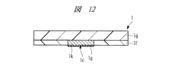
次に、図12、図13および図14は、それぞれSIP基板1のバンプランド1cの構造について示したものであり、バンプランド1cもフリップチップ電極1eと同様に、その側面が絶縁膜であるソルダレジスト膜1fによって囲まれていることが好ましい。
Next, FIG. 12, FIG. 13 and FIG. 14 show the structure of the
バンプランド1cの側面がソルダレジスト膜1fによって囲まれていることにより、バンプランド1cの接続面に形成するはんだボール8の量を抑制することができ、その結果、隣接するはんだボール8間で発生するはんだショートを低減することができる。
Since the side surfaces of the bump lands 1c are surrounded by the solder resist
なお、図13に示すように、バンプランド1cよりソルダレジスト膜1fの高さを高くすることにより、バンプランド1cの接続面に接続するはんだボール8の量をより確実に低減することができ、その結果、バンプランド1c間で発生するはんだショートをより確実に低減することができる。
In addition, as shown in FIG. 13, by making the height of the solder resist
また、図14に示すように、ソルダレジスト膜1fを2層構造として、上層のソルダレジスト膜1fをバンプランド1cの接続面の周縁部に配置することにより、バンプランド1cの接続面に接続するはんだボール8の量をさらに少なくすることができ、その結果、バンプランド1c間で発生するはんだショートをさらに低減することができる。
Further, as shown in FIG. 14, the solder resist
次に、本実施の形態のSIP10に組み込まれるSIP基板1の変形例について説明する。
Next, a modified example of the
図15は変形例の多数個取り基板11(SIP基板1)の最表層(主面1a)と最下層(裏面1b)のそれぞれの配線パターンを示すものである。変形例の多数個取り基板11(SIP基板1)では、裏面1bのバンプランド1cのニッケル−金合金のメッキ膜1gを形成するための電解メッキの給電用配線1hが、裏面1b(最下層)にも形成されている。すなわち、図15の最下層に示すように、バンプランド1cの配置によるその内側の空きスペース(例えば、中央部)を利用し、この空きスペースと切断部20とに広面積パターンによる共通の給電用配線1hを配置し、それぞれをリード状の給電用配線1hによって接続している。この場合、裏面1bにおいて外周部に配置されたバンプランド1cから中央部の広面積パターンによる共通の給電用配線1hに向かってリード状の給電用配線1hが延在している。さらに、中央部の広面積パターンの給電用配線1hと複数のバンプランド1cがそれぞれリード状の給電用配線1hによって接続されている。このようにして裏面1bの全てのバンプランド1cを、中央部もしくは切断部20の広面積パターンの共通の給電用配線1hにリード状の給電用配線1hを介して接続する。
FIG. 15 shows the wiring patterns of the outermost layer (main surface 1a) and the lowermost layer (back
なお、最表層では、複数のボンディングパッド1d(フリップチップ電極1eであってもよい)がそれぞれ単独の給電用配線1hによって切断部20の共通の給電用配線1hと接続されている。
In the outermost layer, a plurality of
図15に示すような配線基板において、給電用配線1hを用いて各バンプランド1cに給電を行ってニッケル−金合金の電解メッキのメッキ膜1gを形成し、その後、基板の製造の最終行程にて、ボンディングパッド1d、バンプランド1cおよびフリップチップ電極1eをレジスト膜で覆った状態で、主面1aの切断部20の広面積パターンの給電用配線1h(図15に点線で示すエッチング部22)と、裏面1bの中央部および切断部20の広面積パターンの給電用配線1h(点線で示すエッチング部22)を、図16に示すようにエッチングによって除去する。これにより、主面1aの各ボンディングパッド1dおよび裏面1bの各バンプランド1cは、それぞれ共通の広面積パターンの給電用配線1hから独立した状態となる。
In a wiring board as shown in FIG. 15, a
このように、本実施の形態のSIP10は、給電後にエッチングにより共通の給電用配線1hを除去して製造されたSIP基板1を用いて組み立ててもよい。
As described above, the
また、SIP基板1としては、その裏面1bの各バンプランド1cの表面に、電解メッキによるニッケル−金合金のメッキ膜1gを形成するのではなく、無電解メッキによるニッケル−金合金の無電解メッキ膜を形成したものを用いてもよい。
Further, as the
この無電解メッキを使用した場合、裏面1bの配線パターンの引き回しを簡略化することができるとともに、メッキ用の給電工程を無くすことができるため、SIP基板1の製造の簡素化を図ることができる。さらに、SIP基板1の低コスト化を図ることができる。
When this electroless plating is used, the routing of the wiring pattern on the
以上、本発明者によってなされた発明を発明の実施の形態に基づき具体的に説明したが、本発明は前記発明の実施の形態に限定されるものではなく、その要旨を逸脱しない範囲で種々変更可能であることは言うまでもない。 Although the invention made by the present inventor has been specifically described based on the embodiments of the invention, the present invention is not limited to the embodiments of the invention, and various modifications can be made without departing from the scope of the invention. It goes without saying that it is possible.
例えば、前記実施の形態では、SIP10が3つの半導体チップを有する場合を説明したが、SIP10は、SIP基板1に対してフリップチップ接続される半導体チップと、ワイヤボンディングされる半導体チップとの少なくとも2つの半導体チップを有し、さらに裏面1bに複数のバンプランド1cが形成されていれば他のSIP10またはマルチチップモジュールあるいはマルチチップパッケージなどであってもよい。
For example, in the above-described embodiment, the case where the
本発明は、電子装置および半導体製造技術ならびに基板の製造技術に好適である。 The present invention is suitable for an electronic device, a semiconductor manufacturing technology, and a substrate manufacturing technology.
1 SIP基板(配線基板)
1a 主面
1b 裏面
1c バンプランド(外部端子搭載電極)
1d ボンディングパッド(金属細線接続用電極)
1e フリップチップ電極
1f ソルダレジスト膜(絶縁膜)
1g メッキ膜
1h 給電用配線
1i 金バンプ(バンプ電極)
1j はんだプリコート
1k 銅パターン
1m はんだ粉末
1n 粘着性被膜
1p フラックス
1q コア部(ベース基板)
1r 内部配線
1s ベースビア
1t ビア
1u スルーホール配線
1v レジスト膜(絶縁膜)
1w 絶縁層
1x レジスト膜(絶縁膜)
2 マイコンチップ(第1の半導体チップ)
2a パッド(電極)
2b 主面
2c 裏面
3 メモリチップ(第2の半導体チップ)
3a パッド(電極)
3b 主面
3c 裏面
4 メモリチップ(第3の半導体チップ)
4a パッド(電極)
4b 主面
4c 裏面
5 ワイヤ(金属細線)
6 封止体(第2の樹脂)
7 アンダーフィル樹脂(第1の樹脂)
8 はんだボール(外部端子)
9 ダイボンド材
10 SIP(半導体装置)
11 多数個取り基板(配線基板)
20 切断部
21 製品領域
22 エッチング部
1 SIP board (wiring board)
1a
1d Bonding pad (metal thin wire connection electrode)
1e
1r
1w Insulating
2 Microcomputer chip (first semiconductor chip)
2a Pad (electrode)
2b
3a Pad (electrode)
3b
4a Pad (electrode)
6 Sealing body (second resin)
7 Underfill resin (first resin)
8 Solder balls (external terminals)
9
11 Multiple substrate (wiring board)
20 Cutting
Claims (10)
第2主面、前記第2主面に形成された第1半導体素子、前記第2主面に形成された複数の第1電極、及び前記第2主面とは反対側の第2裏面を有し、前記第2主面が前記配線基板の前記第1主面と対向するように、複数のバンプ電極を介して前記配線基板の前記第1主面上にフリップチップ接続された第1半導体チップと、
第3主面、前記第3主面に形成された第2半導体素子、前記第3主面に形成された複数の第2電極、及び前記第3主面とは反対側の第3裏面を有し、前記第3裏面が前記第1半導体チップの前記第2裏面と対向するように、前記第1半導体チップの前記第2裏面上に配置された第2半導体チップと、
前記第2半導体チップの前記複数の第2電極と、これに対応する前記配線基板の前記複数のボンディングパッドとをそれぞれ電気的に接続する複数のワイヤと、
前記配線基板の前記複数の外部端子搭載電極にそれぞれ搭載された複数の外部端子と、
を含み、
前記複数のボンディングパッドは、前記複数の配線層のうちの1層目に形成され、
前記複数の外部端子搭載電極は、前記複数の配線層のうちの6層目に形成され、
前記複数のボンディングパッドのそれぞれには、電解メッキの第1給電用配線が接続されており、
前記複数の外部端子搭載電極のそれぞれには、電解メッキの第2給電用配線が接続されており、
前記複数のボンディングパッド及び前記複数の外部端子搭載電極のそれぞれの表面には、ニッケル合金のメッキ膜が形成されており、
前記第1給電用配線は、前記複数の配線層のうちの1層目に形成されており、
前記第2給電用配線は、前記複数の配線層のうちの5層目及び6層目のそれぞれに形成されていることを特徴とする半導体装置。 A first main surface, a plurality of wirings formed on the first main surface, a plurality of bonding pads formed on the first main surface, a plurality of flip chip electrodes formed on the first main surface, the first A wiring substrate having a first back surface opposite to the main surface and a plurality of external terminal mounting electrodes formed on the first back surface, the wiring substrate including six wiring layers;
A second main surface; a first semiconductor element formed on the second main surface; a plurality of first electrodes formed on the second main surface; and a second back surface opposite to the second main surface. then, the so second main surface opposed to the first main surface of the wiring substrate, a first semiconductor that is flip-chip connected to said first main surface of the wiring substrate via the bump electrode of the multiple Chips,
A third main surface; a second semiconductor element formed on the third main surface; a plurality of second electrodes formed on the third main surface; and a third back surface opposite to the third main surface. A second semiconductor chip disposed on the second back surface of the first semiconductor chip such that the third back surface faces the second back surface of the first semiconductor chip;
A plurality of wires electrically connecting the plurality of second electrodes of the second semiconductor chip and the plurality of bonding pads of the wiring board corresponding to the second electrodes;
A plurality of external terminals mounted respectively on the plurality of external terminal mounting electrodes of the wiring board,
Including
The plurality of bonding pads are formed in a first layer of the plurality of wiring layers,
The plurality of external terminal mounting electrodes are formed in a sixth layer of the plurality of wiring layers,
Each of the plurality of bonding pads is connected to a first power supply wiring for electrolytic plating,
Each of the plurality of external terminal mounting electrodes is connected to a second power supply wiring for electrolytic plating,
A nickel alloy plating film is formed on each surface of the plurality of bonding pads and the plurality of external terminal mounting electrodes,
The first power supply wiring is formed in a first layer of the plurality of wiring layers,
The second power supply wiring is formed in each of a fifth layer and a sixth layer of the plurality of wiring layers .
Priority Applications (1)
| Application Number | Priority Date | Filing Date | Title |
|---|---|---|---|
| JP2003376415A JP4398225B2 (en) | 2003-11-06 | 2003-11-06 | Semiconductor device |
Applications Claiming Priority (1)
| Application Number | Priority Date | Filing Date | Title |
|---|---|---|---|
| JP2003376415A JP4398225B2 (en) | 2003-11-06 | 2003-11-06 | Semiconductor device |
Related Child Applications (2)
| Application Number | Title | Priority Date | Filing Date |
|---|---|---|---|
| JP2009025463A Division JP4839384B2 (en) | 2009-02-06 | 2009-02-06 | Manufacturing method of semiconductor device |
| JP2009111869A Division JP2009200519A (en) | 2009-05-01 | 2009-05-01 | Semiconductor device |
Publications (3)
| Publication Number | Publication Date |
|---|---|
| JP2005142312A JP2005142312A (en) | 2005-06-02 |
| JP2005142312A5 JP2005142312A5 (en) | 2006-12-21 |
| JP4398225B2 true JP4398225B2 (en) | 2010-01-13 |
Family
ID=34687463
Family Applications (1)
| Application Number | Title | Priority Date | Filing Date |
|---|---|---|---|
| JP2003376415A Expired - Fee Related JP4398225B2 (en) | 2003-11-06 | 2003-11-06 | Semiconductor device |
Country Status (1)
| Country | Link |
|---|---|
| JP (1) | JP4398225B2 (en) |
Families Citing this family (3)
| Publication number | Priority date | Publication date | Assignee | Title |
|---|---|---|---|---|
| JP4571679B2 (en) * | 2008-01-18 | 2010-10-27 | Okiセミコンダクタ株式会社 | Semiconductor device |
| EP3891806B1 (en) * | 2019-04-15 | 2026-04-08 | Yangtze Memory Technologies Co., Ltd. | Unified semiconductor devices having processor and heterogeneous memories and methods for forming the same |
| CN114005760A (en) * | 2021-11-05 | 2022-02-01 | 苏州群策科技有限公司 | Preparation method of semiconductor packaging substrate |
Family Cites Families (13)
| Publication number | Priority date | Publication date | Assignee | Title |
|---|---|---|---|---|
| JPH09199630A (en) * | 1996-01-19 | 1997-07-31 | Toshiba Corp | Multilayer wiring board |
| JP2000114412A (en) * | 1998-10-06 | 2000-04-21 | Shinko Electric Ind Co Ltd | Circuit board manufacturing method |
| JP2001284783A (en) * | 2000-03-30 | 2001-10-12 | Shinko Electric Ind Co Ltd | Surface mounting substrate and surface mounting structure |
| JP3871853B2 (en) * | 2000-05-26 | 2007-01-24 | 株式会社ルネサステクノロジ | Semiconductor device and operation method thereof |
| JP2002026174A (en) * | 2000-07-11 | 2002-01-25 | Shinko Electric Ind Co Ltd | Circuit board manufacturing method |
| JP4465884B2 (en) * | 2001-01-22 | 2010-05-26 | ソニー株式会社 | Semiconductor device and manufacturing method thereof |
| JP2002343818A (en) * | 2001-05-14 | 2002-11-29 | Shinko Electric Ind Co Ltd | BGA type wiring board, method of manufacturing the same, and method of manufacturing semiconductor device |
| JP4012375B2 (en) * | 2001-05-31 | 2007-11-21 | 株式会社ルネサステクノロジ | Wiring board and manufacturing method thereof |
| CN100407422C (en) * | 2001-06-07 | 2008-07-30 | 株式会社瑞萨科技 | Semiconductor device and method for manufacturing the same |
| JP3500132B2 (en) * | 2001-06-15 | 2004-02-23 | 日本アビオニクス株式会社 | Flip chip mounting method |
| JP2003007902A (en) * | 2001-06-21 | 2003-01-10 | Shinko Electric Ind Co Ltd | Electronic component mounting board and mounting structure |
| JP2003086735A (en) * | 2001-06-27 | 2003-03-20 | Shinko Electric Ind Co Ltd | Wiring board with position information, method for manufacturing the same, and method for manufacturing semiconductor device |
| JP2003234451A (en) * | 2002-02-06 | 2003-08-22 | Matsushita Electric Ind Co Ltd | Semiconductor device and method of manufacturing the same |
-
2003
- 2003-11-06 JP JP2003376415A patent/JP4398225B2/en not_active Expired - Fee Related
Also Published As
| Publication number | Publication date |
|---|---|
| JP2005142312A (en) | 2005-06-02 |
Similar Documents
| Publication | Publication Date | Title |
|---|---|---|
| JP4790157B2 (en) | Semiconductor device | |
| CN102867800B (en) | Functional chip is connected to packaging part to form package on package | |
| US7411281B2 (en) | Integrated circuit device package having both wire bond and flip-chip interconnections and method of making the same | |
| JP2004228323A (en) | Semiconductor device | |
| JP2001257307A (en) | Semiconductor device | |
| JP2002343899A (en) | Substrate for semiconductor package, semiconductor package | |
| JP4477966B2 (en) | Manufacturing method of semiconductor device | |
| US8008765B2 (en) | Semiconductor package having adhesive layer and method of manufacturing the same | |
| US7501707B2 (en) | Multichip semiconductor package | |
| JP2010287710A (en) | Semiconductor device and manufacturing method thereof | |
| KR100573302B1 (en) | Package Stack Using Wire Bonding and Manufacturing Method Thereof | |
| JP4033968B2 (en) | Multiple chip mixed semiconductor device | |
| JP5096683B2 (en) | Semiconductor device | |
| JP4398225B2 (en) | Semiconductor device | |
| JP4494249B2 (en) | Semiconductor device | |
| CN100524741C (en) | Stacked package structure | |
| JP2013201218A (en) | Semiconductor device and semiconductor module using the same | |
| JP4839384B2 (en) | Manufacturing method of semiconductor device | |
| JP2009200519A (en) | Semiconductor device | |
| JPH10173087A (en) | Semiconductor integrated circuit device | |
| JP2006202997A (en) | Semiconductor device and manufacturing method thereof | |
| JP5297445B2 (en) | Semiconductor device | |
| JP3600138B2 (en) | Semiconductor device | |
| KR20020028473A (en) | Stack package | |
| JP2009246313A (en) | Semiconductor device and manufacturing method therefor |
Legal Events
| Date | Code | Title | Description |
|---|---|---|---|
| A521 | Request for written amendment filed |
Free format text: JAPANESE INTERMEDIATE CODE: A523 Effective date: 20061102 |
|
| A621 | Written request for application examination |
Free format text: JAPANESE INTERMEDIATE CODE: A621 Effective date: 20061102 |
|
| A977 | Report on retrieval |
Free format text: JAPANESE INTERMEDIATE CODE: A971007 Effective date: 20070403 |
|
| A131 | Notification of reasons for refusal |
Free format text: JAPANESE INTERMEDIATE CODE: A131 Effective date: 20081209 |
|
| A521 | Request for written amendment filed |
Free format text: JAPANESE INTERMEDIATE CODE: A523 Effective date: 20090206 |
|
| A131 | Notification of reasons for refusal |
Free format text: JAPANESE INTERMEDIATE CODE: A131 Effective date: 20090303 |
|
| A521 | Request for written amendment filed |
Free format text: JAPANESE INTERMEDIATE CODE: A523 Effective date: 20090501 |
|
| A02 | Decision of refusal |
Free format text: JAPANESE INTERMEDIATE CODE: A02 Effective date: 20090602 |
|
| A521 | Request for written amendment filed |
Free format text: JAPANESE INTERMEDIATE CODE: A523 Effective date: 20090821 |
|
| A911 | Transfer to examiner for re-examination before appeal (zenchi) |
Free format text: JAPANESE INTERMEDIATE CODE: A911 Effective date: 20090910 |
|
| TRDD | Decision of grant or rejection written | ||
| A01 | Written decision to grant a patent or to grant a registration (utility model) |
Free format text: JAPANESE INTERMEDIATE CODE: A01 Effective date: 20091006 |
|
| A01 | Written decision to grant a patent or to grant a registration (utility model) |
Free format text: JAPANESE INTERMEDIATE CODE: A01 |
|
| A61 | First payment of annual fees (during grant procedure) |
Free format text: JAPANESE INTERMEDIATE CODE: A61 Effective date: 20091022 |
|
| FPAY | Renewal fee payment (event date is renewal date of database) |
Free format text: PAYMENT UNTIL: 20121030 Year of fee payment: 3 |
|
| R150 | Certificate of patent or registration of utility model |
Ref document number: 4398225 Country of ref document: JP Free format text: JAPANESE INTERMEDIATE CODE: R150 Free format text: JAPANESE INTERMEDIATE CODE: R150 |
|
| FPAY | Renewal fee payment (event date is renewal date of database) |
Free format text: PAYMENT UNTIL: 20121030 Year of fee payment: 3 |
|
| S111 | Request for change of ownership or part of ownership |
Free format text: JAPANESE INTERMEDIATE CODE: R313111 |
|
| FPAY | Renewal fee payment (event date is renewal date of database) |
Free format text: PAYMENT UNTIL: 20121030 Year of fee payment: 3 |
|
| R350 | Written notification of registration of transfer |
Free format text: JAPANESE INTERMEDIATE CODE: R350 |
|
| FPAY | Renewal fee payment (event date is renewal date of database) |
Free format text: PAYMENT UNTIL: 20121030 Year of fee payment: 3 |
|
| FPAY | Renewal fee payment (event date is renewal date of database) |
Free format text: PAYMENT UNTIL: 20131030 Year of fee payment: 4 |
|
| S531 | Written request for registration of change of domicile |
Free format text: JAPANESE INTERMEDIATE CODE: R313531 |
|
| R350 | Written notification of registration of transfer |
Free format text: JAPANESE INTERMEDIATE CODE: R350 |
|
| LAPS | Cancellation because of no payment of annual fees |