JP4323002B2 - Imaging device - Google Patents
Imaging device Download PDFInfo
- Publication number
- JP4323002B2 JP4323002B2 JP14651799A JP14651799A JP4323002B2 JP 4323002 B2 JP4323002 B2 JP 4323002B2 JP 14651799 A JP14651799 A JP 14651799A JP 14651799 A JP14651799 A JP 14651799A JP 4323002 B2 JP4323002 B2 JP 4323002B2
- Authority
- JP
- Japan
- Prior art keywords
- focus detection
- imaging
- image
- image sensor
- region
- Prior art date
- Legal status (The legal status is an assumption and is not a legal conclusion. Google has not performed a legal analysis and makes no representation as to the accuracy of the status listed.)
- Expired - Fee Related
Links
- 238000003384 imaging method Methods 0.000 title claims description 106
- 238000001514 detection method Methods 0.000 claims description 110
- 230000003287 optical effect Effects 0.000 claims description 49
- 230000004907 flux Effects 0.000 claims description 12
- 238000004364 calculation method Methods 0.000 description 20
- 238000012546 transfer Methods 0.000 description 20
- 238000012545 processing Methods 0.000 description 19
- 238000000034 method Methods 0.000 description 17
- 230000008569 process Effects 0.000 description 14
- 238000009825 accumulation Methods 0.000 description 12
- 238000010586 diagram Methods 0.000 description 12
- 238000005259 measurement Methods 0.000 description 11
- 210000001747 pupil Anatomy 0.000 description 9
- 238000005375 photometry Methods 0.000 description 7
- 230000000875 corresponding effect Effects 0.000 description 5
- GGCZERPQGJTIQP-UHFFFAOYSA-N sodium;9,10-dioxoanthracene-2-sulfonic acid Chemical group [Na+].C1=CC=C2C(=O)C3=CC(S(=O)(=O)O)=CC=C3C(=O)C2=C1 GGCZERPQGJTIQP-UHFFFAOYSA-N 0.000 description 5
- 230000002093 peripheral effect Effects 0.000 description 4
- 230000006835 compression Effects 0.000 description 3
- 238000007906 compression Methods 0.000 description 3
- 230000002596 correlated effect Effects 0.000 description 3
- 238000005070 sampling Methods 0.000 description 3
- 239000004065 semiconductor Substances 0.000 description 3
- 239000000758 substrate Substances 0.000 description 3
- 101000885321 Homo sapiens Serine/threonine-protein kinase DCLK1 Proteins 0.000 description 2
- 102100039758 Serine/threonine-protein kinase DCLK1 Human genes 0.000 description 2
- 238000006243 chemical reaction Methods 0.000 description 2
- 230000001276 controlling effect Effects 0.000 description 2
- 230000006837 decompression Effects 0.000 description 2
- 238000005516 engineering process Methods 0.000 description 2
- 230000011514 reflex Effects 0.000 description 2
- 229910052710 silicon Inorganic materials 0.000 description 2
- 239000010703 silicon Substances 0.000 description 2
- BQCADISMDOOEFD-UHFFFAOYSA-N Silver Chemical compound [Ag] BQCADISMDOOEFD-UHFFFAOYSA-N 0.000 description 1
- 230000009471 action Effects 0.000 description 1
- 238000012937 correction Methods 0.000 description 1
- 238000009792 diffusion process Methods 0.000 description 1
- 230000000694 effects Effects 0.000 description 1
- 230000006870 function Effects 0.000 description 1
- 239000004973 liquid crystal related substance Substances 0.000 description 1
- 238000004519 manufacturing process Methods 0.000 description 1
- 230000009467 reduction Effects 0.000 description 1
- 230000035945 sensitivity Effects 0.000 description 1
- 229910052709 silver Inorganic materials 0.000 description 1
- 239000004332 silver Substances 0.000 description 1
Images




Classifications
-
- G—PHYSICS
- G03—PHOTOGRAPHY; CINEMATOGRAPHY; ANALOGOUS TECHNIQUES USING WAVES OTHER THAN OPTICAL WAVES; ELECTROGRAPHY; HOLOGRAPHY
- G03B—APPARATUS OR ARRANGEMENTS FOR TAKING PHOTOGRAPHS OR FOR PROJECTING OR VIEWING THEM; APPARATUS OR ARRANGEMENTS EMPLOYING ANALOGOUS TECHNIQUES USING WAVES OTHER THAN OPTICAL WAVES; ACCESSORIES THEREFOR
- G03B3/00—Focusing arrangements of general interest for cameras, projectors or printers
-
- G—PHYSICS
- G02—OPTICS
- G02B—OPTICAL ELEMENTS, SYSTEMS OR APPARATUS
- G02B7/00—Mountings, adjusting means, or light-tight connections, for optical elements
- G02B7/28—Systems for automatic generation of focusing signals
Landscapes
- Physics & Mathematics (AREA)
- General Physics & Mathematics (AREA)
- Optics & Photonics (AREA)
- Automatic Focus Adjustment (AREA)
- Focusing (AREA)
- Solid State Image Pick-Up Elements (AREA)
- Studio Devices (AREA)
- Measurement Of Optical Distance (AREA)
Description
【0001】
【発明の属する技術分野】
この発明は電子的撮像素子を用いて撮影を行う撮像装置に関し、より詳細には該撮像装置に使用される焦点検出装置に関するものである。
【0002】
【従来の技術】
従来より、電子的撮像素子を使用する撮像装置が多数開示されている。
【0003】
例えば、特開平8−262564号公報には、被写体観察のための結像系を1つの撮影レンズからの光束によって行う一眼レフレックスタイプのカメラであって、映像記録部に銀塩フィルムの代わりに固体撮像素子を用いた撮像装置が開示されている。この撮像装置には、TTL位相差AF方式が採用されている。
【0004】
また、特開平9−274136号公報には、撮影レンズ内にTTL位相差検出ユニットを内蔵しているビデオカメラが開示されている。
【0005】
更に、特開平7−281080号公報には、電子ビューファインダを有する銀塩カメラが開示されている。これは、電子ビューファインダ用の撮像素子に測距用の受光素子領域を設け、電子ビューファインダ用の光束を分割して測距用受光素子に導き、焦点検出を行うものである。
【0006】
【発明が解決しようとする課題】
しかしながら、上記特開平8−262564号に記載の一眼レフレックスカメラタイプの撮像装置や、上記特開平9−274136号に記載のビデオカメラでは、TTL位相差検出用の専用AFセンサを撮像素子とは別に有している。そのため、コストアップするという課題を有している。
【0007】
また、上記特開平7−281080号に開示のカメラは、電子ビューファインダを有する銀フィルムカメラに限定されている。
【0008】
更に、測距用受光素子領域についての具体的な記述はないが、撮像領域と同一の構成をすると以下のような課題がある。
【0009】
通常、撮像素子上にはマイクロレンズが配置されており、測距用受光素子領域では、AF光学系の焦点検出光束がマイクロレンズによりけられて周辺減光が極めて大きくなり、測距精度が大幅に劣化したり測距不能となる課題がある。
【0010】
更に、通常、撮像素子上には受光素子前面に、規則的に色フィルタが配置されており、測距用受光素子領域に於いては色フィルタの配列が考慮されていないので、色情報が混在して測距不能となる課題がある。
【0011】
また、撮像素子の画素ピッチは、撮影画像の必要画質に基いて設定されているので、測距用受光素子領域に於いては、必要な測距精度に応じた画素ピッチと比較して細かすぎるので、オーバースペックとなってしまう。
【0012】
加えて、画素面積が小さいため蓄積時間が長く必要になる。また、測距演算に使用する画素数が多いので、測距演算時間が増大し、測距に要するタイムラグが増大するという課題を有している。
【0013】
したがってこの発明は、上記実状に鑑みてなされたものであり、電子的撮像素子により撮像を行う撮像装置に於いて、撮像素子と別に専用のAFセンサを必要とせず、より低コスト化すると共に、焦点検出精度を向上させ、焦点調節によるタイムラグを減少させることのできる撮像装置を提供することを目的とする。
【0014】
【課題を解決するための手段】
すなわち、第1の本発は、撮影レンズと、この撮影レンズを通過した光束を電子的に撮像する撮像領域及び焦点検出領域とを有する撮像素子と、この撮像素子の撮像領域及び焦点検出領域のうち撮像領域の前面にのみ配置された色フィルタと、上記撮影レンズを通過した被写体光束の少なくとも一部の光束を上記撮像素子上の焦点検出領域に再結像させる焦点検出光学系と、上記撮影レンズを通過した被写体光束の少なくとも一部を上記焦点検出光学系に導く光学部材と、上記撮像素子の出力に基いて焦点検出を行う焦点検出手段と、を具備することを特徴とする。
【0016】
第1の発明の撮像装置にあっては、撮影レンズを通過した光束を電子的に撮像する撮像領域及び焦点検出領域とを撮像素子が有している。そして、この撮像素子の撮像領域及び焦点検出領域のうち、撮像領域の前面にのみ色フィルタが配置されている。また、上記撮影レンズを通過した被写体光束の少なくとも一部の光束は、焦点検出光学系によって上記撮像素子上の焦点検出領域に再結像される。更に、上記撮影レンズを通過した被写体光束の少なくとも一部は、光学部材によって上記焦点検出光学系に導かれる。そして、上記撮像素子の出力に基いて、焦点検出手段によって焦点検出が行われる。
【0018】
【発明の実施の形態】
以下、図面を参照してこの発明の実施の形態について説明する。
【0019】
図2は、この発明の第1の実施の形態を示すもので、撮像装置が適用された電子的撮像素子を有するカメラの光路図である。
【0020】
図2に於いて、撮像光学系11は、焦点調節光学系11a、絞り11bを有して成る。絞り11bは、所定の絞り開口を保持することが可能であると共に、完全に閉じて遮光する機能を有している。
【0021】
撮影光学系11を通過した被写体光束は、赤外光成分をカットする赤外光カットフィルタ12、モアレを低減させる光学的LPF(ローパスフィルタ)13を通過した後、ハーフミラーであるメインミラー14でその一部が反射される。
【0022】
メインミラー14で反射された一部の被写体光束は、ピント板15、コンデンサレンズ16を通ってペンタプリズム17により正立像となり、接眼レンズ18を通して撮影者に被写体像が観察されるようになっている。
【0023】
一方、メインミラー14を透過した一部の被写体光束は、全反射ミラーであるサブミラー19によって反射され、焦点検出光学系21に導かれる。
【0024】
焦点検出光学系21は、視野マスク22と、フィールドレンズ23と、全反射ミラー24と、瞳マスク25と、再結像レンズ26とから構成される。この焦点検出光学系21は、焦点検出光束を撮像素子30上の焦点検出領域に再結像させる。
【0025】
また、被写体像を撮影する時には、メインミラー14及びサブミラー19は値図示矢印A方向に回転して同図の破線で示される位置に退避される。これにより、撮影光束は撮像素子30の後述する撮像領域38に導かれる。
【0026】
次に、焦点検出光学系について説明する。
【0027】
図3は、焦点検出光学系(位相差検出光学系)21の構成を示したもので、(a)は各レンズと像との関係を示した図、(b)は該位相差検出光学系の斜視図である。
【0028】
尚、図3に於いては、上述したメインミラー14、サブミラー19、全反射ミラー24等は、説明の簡略化のために省略している。
【0029】
図3に於いて、左側より光束が入射されるが、撮影レンズ11の後方に、視野マスク31、フィールドレンズ32、撮影レンズ11の光軸に対して略対称に配置された開口部33a、33bを有する瞳マスク33、該瞳マスク33の開口部33a、33bに対応してその後方に配置された再結像レンズ34a、34bが、順次配置されている。
【0030】
撮影レンズ11の射出瞳Hの領域Ha、Hbを通過して入射された被写体光束は、視野マスク31、フィールドレンズ32、瞳マスク33の開口部33a、33b及び再結像レンズ34a、34bを通過して撮像素子30の焦点検出領域36(P)上に再結像される。
【0031】
撮影レンズ11が合焦、すなわち結像面G上に被写体像Iが形成される場合、その被写体像Iは、フィールドレンズ32及び再結像レンズ34a、34bによって、光軸Oに対して垂直な2次結像面である撮像素子30の焦点検出領域36(P)上の領域37a、37bに再結像されて、第1像I1 、第2像I2 となる。
【0032】
撮影レンズ11が前ピン、すなわち結像面Gの前方に被写体像Fが形成される場合、その被写体像Fは、互いにより光軸Oに近付いた形で光軸Oに対して垂直に再結像され、第1像F1 、第2像F2 となる。
【0033】
更に、撮影レンズ11が後ピン、すなわち結像面Gの後方に被写体像Rが形成される場合、その被写体像Rは、互いにより光軸Oから離れた形で、光軸Oに対して垂直に再結像されて、第1像R1 、第2像R2 となる。
【0034】
これら第1像と第2像の間隔を検出することにより、撮影レンズ11の合焦状態を前ピン、後ピンを含めて検出することができる。具体的には、上記第1像と第2像の光強度分布が撮像素子30の焦点検出領域36の画像データ出力により求められて、両像の間隔が測定される。
【0035】
尚、図3(b)に於いて、38は撮像素子30の撮像領域である。
【0036】
また、図4は、撮影画面40内の焦点検出領域41を示した図である。
【0037】
次に、図5を参照して、このカメラの電気的ブロック図について説明する。
【0038】
マイクロコンピュータ45は、このカメラの制御装置であり、内部にCPU(中央処理装置)46、ROM47、RAM48、A/Dコンバータ(ADC)49及びEEPROM50等を有するコントローラである。このカメラは、マイクロコンピュータ45の内部のROM47に格納されているシーケンスプログラムに従って、一連の動作を行っている。
【0039】
上記EEPROM50は、焦点調節、測光・露出演算、オートホワイトバランス(AWD)等に関する補正データをカメラ毎に記憶しているものである。
【0040】
このマイクロコンピュータ45には、該マイクロコンピュータ45からの司令に基いて、焦点調節光学系11aを駆動するレンズ駆動部52と、マイクロコンピュータ45からの司令に基いて絞り11bを駆動する絞り駆動部53とが接続されている。
【0041】
上記マイクロコンピュータ45には、また、撮像素子(CCD)30に対して駆動信号を出力してその動作を制御するための撮像素子制御部55が接続されている。
【0042】
上記撮像素子30では、撮影光学系11により形成される被写体像を、撮像領域38にて撮像して電気信号に変換する。また、焦点検出領域36に於いて、焦点検出光束を受光して電気信号に変換する。
【0043】
映像信号処理部56は、上記撮像素子30からの画素信号である電気信号を処理して映像信号を作成するためのものである。この映像信号処理部56には、焦点検出演算部57と、記録部58と、測光・露出演算部59と、オートホワイトバランス部60と、表示部61とが接続されている。
【0044】
上記焦点検出演算部57は、上記映像信号処理部56に於いて処理された映像信号に基いて、焦点検出演算を行うためのものである。ここで、焦点検出演算の結果、合焦の判定データやフォーカシングレンズ駆動量等が、マイクロコンピュータ45に送信される。
【0045】
上記記録部58は、上記映像信号処理部56内の後述するプロセス処理回路114から出力される映像信号(画素データ)を記憶するためのものである。また、測光・露出演算部59は、上記映像信号処理部56に於いて処理された映像信号に基いて、測光値、露出制御値を算出する。
【0046】
また、撮像素子制御部55は、上記測光・露出演算部59の出力であるシャッタスピードに基いて、撮影時の撮像素子30の電子シャッタを制御する。そして、上記測光部・露出演算部59の露出演算により算出された絞り値データに基いて、撮影時に撮影光学系11内の絞り11bの制御が行われる。
【0047】
オートホワイトバランス部60は、上記映像信号処理部56に於いて処理された映像信号に基いて、ホワイトバランスを自動的に制御するためのものである。更に、表示部61は、撮像素子30により撮像された映像やカメラ内部の情報をLCD等の表示素子により表示するためのもので、マイクロコンピュータ45により制御される。
【0048】
更に、上記マイクロコンピュータ45には、ファーストレリーズスイッチ(1RSW)63と、セカンドレリーズスイッチ(2RSW)64とが接続されている。ファーストレリーズスイッチ63及びセカンドレリーズスイッチ64は、図示されないレリーズ釦に連動したスイッチであり、レリーズ釦の第1段階の押し下げによりファーストレリーズスイッチ63がオンし、引続いて第2段階の押し下げでセカンドレリーズスイッチ64がオンするようになっている。
【0049】
マイクロコンピュータ45は、ファーストレリーズスイッチ63のオンで測光、AF動作を行い、セカンドレリーズスイッチ64のオンで露出動作と画像記録動作を行う。
【0050】
次に、上述した撮像素子30の構成について説明する。
【0051】
図6に於いて、撮像素子30の撮像領域38は、水平方向と垂直方向に二次元状に配置されたフォトダイオード71と、該フォトダイオード71に蓄積された電荷を垂直シフトレジスタ73に転送するトランスファーゲート72と、転送された電荷を順次垂直方向に転送する垂直シフトレジスタ73と、この垂直シフトレジスタ73により垂直方向に転送された電荷を水平方向に順次転送する水平シフトレジスタ74と、この水平シフトレジスタ74により水平方向に転送された電荷を電圧信号に変換して出力する出力部75とから構成されている。
【0052】
撮像素子30の焦点検出領域36は、上述した撮像領域38と同様に、水平方向と垂直方向に二次元状に配置されたフォトダイオード76と、該フォトダイオード76に蓄積された電荷を垂直シフトレジスタ78に転送するトランスファーゲート77と、転送された電荷を順次垂直方向に転送する垂直シフトレジスタ78と、この垂直シフトレジスタ78により垂直方向に転送された電荷を水平方向に順次転送する水平シフトレジスタ79と、この水平シフトレジスタ79により水平方向に転送された電荷を電圧信号に変換して出力する出力部80とから構成されている。
【0053】
撮像領域38の受光素子フォトダイオード71の前面には、それぞれマイクロレンズが構成されている。
【0054】
撮像素子の光感度を向上させる技術として、各フォトダイオードに対応した位置にマイクロレンズを設けることにより、入射光を効率よく受光部に集光する、いわゆるオンチップマイクロレンズと呼ばれる技術が確立されている。
【0055】
図1(a)は、オンチップマイクロレンズを形成した撮像素子30の撮像領域38の水平方向、すなわち垂直シフトレジスタの転送方向と直交する方向に於ける断面図である。
【0056】
シリコンから成る半導体基板85内に、拡散層等により、垂直シフトレジスタ95を構成する電荷転送部86と、受光部87を構成するフォトダイオードが形成される。上記電荷転送部86上には、図示されない絶縁膜を介して垂直転送電極88が形成されている。更に、この垂直転送電極88を覆うようにして、遮光膜89が形成されている。尚、上記受光部87は、遮光膜89の開口に対応して形成されている。
【0057】
受光部87上及び遮光膜89上には、両者を覆うようにして透明平坦化層90が形成される。そして、この透明平坦化層90上には、色フィルタ91及び透明平坦化層92が、順次形成される。
【0058】
更に、透明平坦化層92上には、所定の曲率rを有し、焦点距離f1の球面であるマイクロレンズ93が形成されている。
【0059】
また、図1(b)は、焦点検出領域36の水平方向、すなわち垂直シフトレジスタの転送方向と直交する方向に於ける断面図である。
【0060】
図1(b)に示されるように、焦点検出領域36には、上述した撮像領域38のようなマイクロレンズが配置されていない。
【0061】
撮像素子上のマイクロレンズは、上述したように、撮像面に対して垂直に入射する光束に対して有効となるように設定されており、いわゆるテレセントリックな撮影光学系(射出瞳が無限遠の光学系)に対応している。
【0062】
したがって、焦点検出領域36のフォトダイオード上に上記マイクロレンズを配置した場合は、マイクロレンズの作用により焦点検出光学系21の焦点検出光束がけられてしまい、焦点検出領域の周辺部が減光してしまう。このため、焦点検出精度が低下したり焦点検出不能となる。
【0063】
このような課題を解消するため、焦点検出領域36は、以下のように構成される。
【0064】
すなわち、シリコンから成る半導体基板100内に、電荷転送部101と、受光部102を構成するフォトダイオードが形成される。そして、上記電荷転送部101上には、図示されない絶縁膜を介して垂直転送電極103が形成されている。更に、この垂直転送電極103を覆うようにして、遮光膜104が形成されている。尚、上記受光部102は、遮光膜104の開口に対応して形成されている。
【0065】
そして、焦点検出領域36のフォトダイオード上には、マイクロレンズが配置されずに透明平坦化層105が形成される。これにより、焦点検出光学系21の焦点検出光束は、受光部102上に再結像される。
【0066】
また、撮像領域38のフォトダイオード71の前面には、色フィルタ91が配置されている。この色フィルタ91の配列は、図7に示されるように、いわゆるベイヤー配列で構成されている。
【0067】
図7に示される色フィルタの配列に於いて、図中R、G、Bは、それぞれ赤、緑、青を選択的に透過する色フィルタである。
【0068】
一方、焦点検出領域36は、フォトダイオードの前面に色フィルタは配置されていない。これは焦点検出に色情報は必要ないからである。
【0069】
ここで、焦点検出領域36のフォトダイオード76のピッチ及び面積は、撮像領域38のフォトダイオード71のピッチ及び面積より、それぞれ大きい。
【0070】
撮像領域38の画素ピッチをP1とすると、このピッチP1は必要な撮影解像度より決定されるものであるが、焦点検出領域36に於いては画素ピッチはより大きく設定されている。焦点検出領域36の画素ピッチは、必要な焦点検出精度に基いて決定される。
【0071】
焦点検出精度に関しては、公知の補間演算等により、検出ピッチの1/100〜1/200の精度で検出可能であることが知られている。
【0072】
一方、撮像素子として必要な焦点調節精度は、撮像領域38の画素ピッチをP1とすると、2・P1以下の検出精度が必要であることが知られている。したがって、焦点検出領域36のフォトダイオード76の検出ピッチP2(瞳分割方向のピッチ)を、例えば10倍としても、20倍程度の余裕があり(10・P1・(1/100)<<2・P1)、焦点検出精度上の問題はない。
【0073】
また、焦点検出領域36のフォトダイオード76の面積は、撮像領域38のフォトダイオード71の面積より大きく設定されている。
【0074】
これにより、同一照度の被写体光に対する蓄積時間をより短縮することができ、焦点検出動作のタイムラグを縮小している。
【0075】
図8は、映像信号処理部56及びその周辺部の構成を示したブロック図である。
【0076】
図8に於いて、相関2重サンプリング回路(CDS)111は、撮像素子(CCD)30の画像信号からリセットノイズ等を除去するための回路である。この相関2重サンプリング回路111からの出力は、ゲインコントロールアンプ(AMP)112に供給されて所定のゲインで増幅される。
【0077】
上記ゲインコントロールアンプ112の出力は、A/Dコンバータ113にてA/D変換されてデジタル信号に変換される。そして、プロセス処理回路114にて、上記デジタル信号に変換された映像信号に対して、各種の処理が行われる。
【0078】
撮像素子制御部(CCD制御部)55は、撮像素子(CCD)30に対して駆動信号を出力してその動作を制御するもので、タイミングジェネレータ(TG)116及びシグナルジェネレータ(SG)117より構成されている。
【0079】
上記タイミングジェネレータ116は、撮像素子30を駆動するための転送パルス等の駆動信号を発生すると共に、上記相関2重サンプリング回路111のサンプルホールドパルス、上記A/Dコンバータ113のA/D変換タイミングパルスを発生する。シグナルジェネレータ117は、上記タイミングジェネレータ116とマイクロコンピュータ45との同期をとるための信号を発生するものである。
【0080】
上記記録部58は、DRAM118と、圧縮伸長回路119と、記録媒体120とから構成される。
【0081】
DRAM118は、映像信号処理部56内のプロセス処理回路114から出力される映像信号(画素データ)を記憶するメモリである。また、圧縮伸長回路119は、上記DRAM118に蓄積された画素データを、データ量を減らして記録するために圧縮し、また記録媒体120から読出した圧縮データの伸長を行うためのものである。更に、記録媒体120は、上記圧縮された静止画データを記録するためのものである。
【0082】
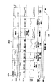
次に、図9のフローチャート及び図10のタイミングチャートを参照して、この発明の実施の形態に於けるカメラのメインルーチンの動作について説明する。
【0083】
図示されない電源スイッチがオンされるか電池がカメラ本体に挿入されると、マイクロコンピュータ45の動作が開始されて、マイクロコンピュータ45内部のROM47に格納されたシーケンスプログラムが実行される。
【0084】
そして、先ず、ステップS1にて、カメラ内の各ブロックの初期化が行われる。次いで、ステップS2に於いて、ファーストレリーズスイッチ(1RSW)63の状態が検出される。
【0085】
ここで、ファーストレリーズスイッチ63がオフの場合は、ステップS3に移行して、撮像素子30の撮像領域38に於ける蓄積(露光)、読出し動作である撮像動作が行われる。
【0086】
続いて、ステップS4にて、映像信号処理部56からの撮像領域38の映像信号に基いて、測光・露出演算部59により測光、露出演算が行われる。そして、本露光(画像記録)時の絞り12の絞り制御値、撮像素子30の電子シャッタスピード等が計算される。その後、上記ステップS2に移行する。
【0087】
上記ステップS2にて、ファーストレリーズスイッチ63がオンされると、ステップS5に移行して、撮像素子30の焦点検出領域36内の領域37a、37bの蓄積動作(AF用露光)が行われる。次いで、ステップS6にて、焦点検出用受光領域37a、37bの画像信号が読出されて、それに基く焦点検出演算が行われる。
【0088】
ステップS7に於いては、焦点検出演算の結果が合焦か非合焦かが判定される。ここで、合焦ならばステップS9に移行する。一方、非合焦の場合はステップS8に移行し、焦点検出演算結果に基いて合焦になるようなフォーカシングレンズ11aの移動量が算出されて駆動される。そして、この後、ステップS2に移行し、AF動作が繰返される。
【0089】
ステップS9では、セカンドレリーズスイッチ(2RSW)64がオンされているか否かが検出される。ここで、セカンドレリーズスイッチ64がオンされている場合はステップS10に移行する。一方、セカンドレリーズスイッチ64がオフの場合は、上記ステップS2に移行し、セカンドレリーズスイッチ64のオンを待ちながらAF動作が継続される。
【0090】
ステップS10以降では、本露光動作が行われる。
【0091】
ステップS10では、マイクロコンピュータ45により絞り駆動部53が制御されて、絞り11bが露出用絞り値に絞り込まれる。
【0092】
次いで、ステップS11にて、撮像素子制御部55により電荷掃出し信号SUBがオフされて、撮像素子30の蓄積がスタートされ、露出演算に基く電子シャッタスピードで制御されて露出(本露光)が行われる。電子シャッタ動作では、撮像素子制御部55によりシャッタスピードに応じた所定のタイミングで電荷転送パルスTGPが発生されて、フォトダイオード71の蓄積電荷が垂直シフトレジスタ73に転送される。
【0093】
そして、ステップS12では、スミアを防止するために、絞り駆動部53が制御されて絞り11bが完全に閉じられ、撮像素子30が遮光状態とされる。
【0094】
次に、ステップS13にて、撮像素子30が遮光された状態で、撮像素子制御部55により、画像読出し信号DCLKが撮像素子30に対して出力される。そして、映像信号処理部56により、上記画像読出し信号DCLKに同期して出力される撮像領域38の画像信号(CCD信号)が、A/D変換されて読出される。
【0095】
ステップS14では、マイクロコンピュータ45によって、絞り駆動部53が制御されて、絞り開放のコマンドが送信されて絞り11bが開放状態にされる。更に、ステップS15では、読出された画像信号の圧縮等の処理が行われ、その後、記録部58内の記録媒体120に格納される。
【0096】
このようにして、一連の撮影動作が終了するとステップS2に戻り、同様に動作が繰返される。
【0097】
次に、焦点検出のための蓄積動作及び焦点検出演算の方法について説明する。
【0098】
図11は、図9のフローチャートのステップS3に於ける焦点検出領域36の蓄積・読出し動作を説明するフローチャートである。
【0099】
先ず、ステップS21では、焦点検出領域36内の有効画素範囲の領域37a、37bに関するデータが、EEPROM50より読出される。尚、上記有効範囲は、カメラ毎に異なるので、製造時に工場にてチェックされ、カメラ毎にEEPROM50に書込まれる。
【0100】
続くステップS22では、前回の蓄積動作による焦点検出領域37a、37b内の画素データが参照されて、適正な画素信号が得られる蓄積時間が求められる。そして、ステップS23では、上記求められた蓄積時間に基いて、撮像素子30の焦点検出領域38の蓄積動作が制御される。
【0101】
ステップS24では、画素信号の読出し動作が行われる。ここで、焦点検出有効領域37a、37b以外の焦点検出領域38の画素信号は、焦点検出に使用されないので、読出し時間を縮小するため高速掃き出し動作が行われる。
【0102】
その後、ステップS25にて、上記EEPROM50に記憶された有効画素範囲である焦点検出領域37a、37bの部分だけ、画素信号が読出される。
【0103】
次に、この発明の第2の実施の形態について説明する。
【0104】
図12は、この発明の第2の実施の形態によるカメラの構成を示す光路図である。この第2の実施の形態は、上述した第1の実施の形態と同様の撮像素子を電子ビューファインダを有する撮像装置に適用したものである。
【0105】
図12に於いて、撮像レンズ11を通過した光束は、全反射ミラーであるメインミラー14で反射されてファインダ系に導かれる。上記メインミラー14で反射された光束は、縮小光学系16を通過し、更にハーフミラー125を透過した光束は、撮像素子30の撮像領域38に入射される。
【0106】
一方、上記ハーフミラー125で反射された光束は、全反射ミラー24で光路が折曲げられた後、瞳マスク26、再結像レンズ26により撮像素子30の焦点検出領域36に再結像される。尚、上記全反射ミラー24、瞳マスク25、再結像レンズ26は、焦点検出光学系21を構成している。
【0107】
上記撮像素子30の焦点検出領域36の画像データは、焦点検出部126によって処理され、焦点検出が行われる。
【0108】
一方、撮像素子30の撮像領域38の画像データは、映像信号処理回路127により読出されて処理されて、液晶表示部128に画像が表示される。
【0109】
銀塩フィルム撮影時は、メインミラー14が退避されて、フォーカルプレーンシャッタ129により銀塩フィルム130に露光される。
【0110】
上述した実施の形態に於いては、撮像素子をCCDとして説明したが、MOS型センサやその他のタイプの固体撮像素子であってもよい。
【0111】
また、銀塩フィルム撮影系と電子的撮像素子により撮影系を両方有するカメラシステムに適用することも可能である。
【0112】
尚、この発明の上記実施の形態によれば、以下の如き構成を得ることができる。
【0113】
(1) メインミラーで分割された光束をサブミラーでミラーボックス底部に導き、位相差方式焦点検出光学系を介して撮像用の撮像素子上に再結像させて位相差検出を行う撮像装置に於いて、
上記撮像素子は上記光束を電子的に撮像する撮像領域と、該撮像素子の出力に基いて焦点検出を行う焦点検出領域とを有し、
上記撮像領域の前面に配置された色フィルタを具備することを特徴とする撮像装置。
【0114】
(2) 上記焦点検出領域の画素ピッチは、上記撮像領域の画素ピッチより大きいことを特徴とする上記(1)に記載の撮像装置。
【0115】
(3) 上記焦点検出領域の画素面積は、上記撮像領域の画素面積より大きいことを特徴とする撮像装置。
【0116】
(4) 上記焦点検出領域の画素面積と上記撮像領域の画素面積が等しく、且つ上記焦点検出領域は画素データを加算して演算に使用することを特徴とする上記(1)に記載の撮像装置。
【0117】
(5) 上記撮像領域は、その前面にマイクロレンズが配置されることを特徴とする上記(1)に記載の撮像装置。
【0118】
【発明の効果】
以上のようにこの発明によれば、撮影レンズを通過した被写体光束を、分岐して撮像素子上に再結像させて位相差検出することにより、専用のAFセンサを必要とせず低コスト化することが可能であると共に、焦点検出精度を向上させ、焦点検出によるタイムラグを減少させた撮像装置を提供することができる。
【図面の簡単な説明】
【図1】この発明の第1の実施の形態による撮像装置の構成を示すもので、(a)はオンチップマイクロレンズを形成した撮像素子30の撮像領域38の水平方向に於ける断面図、(b)は焦点検出領域36の水平方向と直交する方向に於ける断面図である。
【図2】この発明の第1の実施の形態を示すもので、撮像装置が適用された電子的撮像素子を有するカメラの光路図である。
【図3】焦点検出光学系21の構成を示したもので、(a)は各レンズと像との関係を示した図、(b)は該位相差検出光学系の斜視図である。
【図4】撮影画面40内の焦点検出領域41を示した図である。
【図5】第1の実施の形態によるカメラの電気的構成を示すブロック図である。
【図6】撮像素子30の構成について説明する図である。
【図7】色フィルタ91の配列の例を示した図である。
【図8】映像信号処理部56及びその周辺部の構成を示したブロック図である。
【図9】第1の実施の形態に於けるマイクロコンピュータ45のメインルーチンを説明するフローチャートである。
【図10】第1の実施の形態の撮像動作を説明するタイミングチャートである。
【図11】図9のフローチャートのステップS3に於ける焦点検出領域36の蓄積・読出し動作を説明するフローチャートである。
【図12】この発明の第2の実施の形態によるカメラの構成を示す光路図である。
【符号の説明】
11 撮像光学系、
11a 焦点調節光学系、
11b 絞り、
12 赤外光カットフィルタ、
13 光学的LPF(ローパスフィルタ)、
14 メインミラー、
15 ピント板、
16 コンデンサレンズ、
17 ペンタプリズム、
18 接眼レンズ、
19 サブミラー、
21 焦点検出光学系、
22、31 視野マスク、
23、32 フィールドレンズ、
24 全反射ミラー、
25、33 瞳マスク、
26、34a、34b 再結像レンズ、
30 撮像素子、
33a、33b 開口部、
36 焦点検出領域、
38 撮像領域、
45 マイクロコンピュータ、
46 CPU(中央処理装置)、
47 ROM、
48 RAM、
49 A/Dコンバータ(ADC)、
50 EEPROM、
52 レンズ駆動部、
53 絞り駆動部、
55 撮像素子制御部、
56 映像信号処理部、
57 焦点検出演算部、
58 記録部、
59 測光・露出演算部、
60 オートホワイトバランス(AWB)部、
61 表示部、
63 ファーストレリーズスイッチ(1RSW)、
64 セカンドレリーズスイッチ(2RSW)、
71、76 フォトダイオード、
72、77 トランスファーゲート、
73、78 垂直シフトレジスタ、
74、79 水平シフトレジスタ、
75、80 出力部、
85、100 半導体基板、
86、101 電荷転送部、
87、102 受光部、
88、103 垂直転送電極、
89、104 遮光膜、
90、92、105 透明平坦化層、
91 色フィルタ、
93 マイクロレンズ。[0001]
BACKGROUND OF THE INVENTION
The present invention relates to an imaging device that performs imaging using an electronic imaging device, and more particularly to a focus detection device used in the imaging device.
[0002]
[Prior art]
Conventionally, a large number of imaging devices using an electronic imaging device have been disclosed.
[0003]
For example, Japanese Patent Application Laid-Open No. 8-262564 discloses a single-lens reflex type camera in which an imaging system for observing an object is performed by a light beam from one photographing lens, and a video recording unit is replaced with a silver salt film. An imaging apparatus using a solid-state imaging element is disclosed. This imaging apparatus employs a TTL phase difference AF method.
[0004]
Japanese Laid-Open Patent Publication No. 9-274136 discloses a video camera in which a TTL phase difference detection unit is built in a photographing lens.
[0005]
Further, JP-A-7-281080 discloses a silver salt camera having an electronic viewfinder. In this method, a light receiving element region for distance measurement is provided in an image sensor for electronic viewfinder, and a light beam for electronic viewfinder is divided and guided to a light receiving element for distance measurement to perform focus detection.
[0006]
[Problems to be solved by the invention]
However, in the single-lens reflex camera type imaging apparatus described in the above-mentioned Japanese Patent Application Laid-Open No. 8-262564 and the video camera described in the above-mentioned Japanese Patent Application Laid-Open No. 9-274136, the dedicated AF sensor for detecting the TTL phase difference is an imaging device. I have it separately. Therefore, there is a problem of increasing the cost.
[0007]
Further, the camera disclosed in the above-mentioned JP-A-7-281080 is limited to a silver film camera having an electronic viewfinder.
[0008]
Furthermore, although there is no specific description about the light receiving element region for distance measurement, there is the following problem when the same configuration as the imaging region is provided.
[0009]
Normally, a microlens is placed on the image sensor, and in the light-receiving element area for distance measurement, the focus detection light beam of the AF optical system is scattered by the microlens, resulting in extremely large peripheral dimming, greatly improving distance measurement accuracy. However, there is a problem that the distance is deteriorated or cannot be measured.
[0010]
Further, normally, color filters are regularly arranged on the front surface of the light receiving element on the image pickup element, and the color filter arrangement is not taken into consideration in the light receiving element area for distance measurement, so color information is mixed. As a result, there is a problem that distance measurement is impossible.
[0011]
In addition, since the pixel pitch of the image sensor is set based on the required image quality of the captured image, in the light receiving element area for distance measurement, it is too fine compared with the pixel pitch corresponding to the required distance measurement accuracy. So it becomes over spec.
[0012]
In addition, since the pixel area is small, a long accumulation time is required. Further, since the number of pixels used for the distance measurement calculation is large, there is a problem that the distance calculation time increases, and the time lag required for the distance measurement increases.
[0013]
Accordingly, the present invention has been made in view of the above circumstances, and in an imaging apparatus that performs imaging with an electronic imaging element, a dedicated AF sensor is not required separately from the imaging element, and the cost is further reduced. An object of the present invention is to provide an imaging apparatus capable of improving focus detection accuracy and reducing a time lag due to focus adjustment.
[0014]
[Means for Solving the Problems]
That is, in the first embodiment, an imaging device having an imaging lens, an imaging region and a focus detection region for electronically imaging a light beam that has passed through the imaging lens, and an imaging region and a focus detection region of the imaging device. It was placed only in front of the imaging area Color filter A focus detection optical system that re-images at least a part of the subject light flux that has passed through the photographing lens onto a focus detection region on the image sensor, and at least a part of the subject light flux that has passed through the photographing lens. An optical member that leads to a focus detection optical system, and a focus detection unit that performs focus detection based on the output of the imaging device are provided.
[0016]
In the image pickup apparatus of the first invention, the image pickup element has an image pickup region and a focus detection region for electronically picking up the light beam that has passed through the photographing lens. Of the imaging area and focus detection area of this imaging device, only on the front side of the imaging area Color filter Is arranged. In addition, at least a part of the subject light beam that has passed through the photographing lens is re-imaged in the focus detection region on the image sensor by the focus detection optical system. Further, at least a part of the subject luminous flux that has passed through the photographing lens is guided to the focus detection optical system by an optical member. Based on the output of the image sensor, focus detection is performed by the focus detection means.
[0018]
DETAILED DESCRIPTION OF THE INVENTION
Embodiments of the present invention will be described below with reference to the drawings.
[0019]
FIG. 2 shows a first embodiment of the present invention, and is an optical path diagram of a camera having an electronic image pickup element to which an image pickup apparatus is applied.
[0020]
In FIG. 2, the imaging
[0021]
The subject luminous flux that has passed through the photographing
[0022]
A part of the subject luminous flux reflected by the
[0023]
On the other hand, a part of the subject luminous flux that has passed through the
[0024]
The focus detection
[0025]
Further, when taking a subject image, the
[0026]
Next, the focus detection optical system will be described.
[0027]
3A and 3B show the configuration of the focus detection optical system (phase difference detection optical system) 21. FIG. 3A shows the relationship between each lens and the image, and FIG. 3B shows the phase difference detection optical system. FIG.
[0028]
In FIG. 3, the
[0029]
In FIG. 3, a light beam is incident from the left side, but
[0030]
The subject luminous flux incident through the areas Ha and Hb of the exit pupil H of the photographing
[0031]
When the photographing
[0032]
When the
[0033]
Further, when the subject image R is formed behind the
[0034]
By detecting the distance between the first image and the second image, the in-focus state of the
[0035]
In FIG. 3B,
[0036]
FIG. 4 is a diagram showing a focus detection area 41 in the shooting screen 40.
[0037]
Next, an electrical block diagram of the camera will be described with reference to FIG.
[0038]
The
[0039]
The
[0040]
The
[0041]
The
[0042]
In the
[0043]
The video
[0044]
The focus
[0045]
The
[0046]
Further, the image
[0047]
The auto
[0048]
Further, a first release switch (1RSW) 63 and a second release switch (2RSW) 64 are connected to the
[0049]
The
[0050]
Next, the configuration of the
[0051]
In FIG. 6, the
[0052]
The
[0053]
Microlenses are respectively formed on the front surface of the light receiving element photodiode 71 in the
[0054]
As a technology to improve the optical sensitivity of the image sensor, a technology called so-called on-chip microlens has been established that condenses incident light efficiently on the light receiving part by providing a microlens at a position corresponding to each photodiode. Yes.
[0055]
FIG. 1A is a cross-sectional view in the horizontal direction of the
[0056]
A
[0057]
A transparent planarization layer 90 is formed on the
[0058]
Further, a microlens 93 having a predetermined curvature r and a spherical surface having a focal length f1 is formed on the transparent planarizing layer 92.
[0059]
FIG. 1B is a cross-sectional view in the horizontal direction of the
[0060]
As shown in FIG. 1B, the
[0061]
As described above, the microlens on the image sensor is set so as to be effective for a light beam incident perpendicularly to the imaging surface, and a so-called telecentric imaging optical system (an optical system with an exit pupil at infinity). System).
[0062]
Therefore, when the micro lens is arranged on the photodiode in the
[0063]
In order to solve such a problem, the
[0064]
In other words, the
[0065]
Then, on the photodiode in the
[0066]
In addition, a color filter 91 is disposed in front of the photodiode 71 in the
[0067]
In the color filter arrangement shown in FIG. 7, R, G, and B in the figure are color filters that selectively transmit red, green, and blue, respectively.
[0068]
On the other hand, in the
[0069]
Here, the pitch and area of the
[0070]
Assuming that the pixel pitch of the
[0071]
Regarding the focus detection accuracy, it is known that the detection can be performed with an accuracy of 1/100 to 1/200 of the detection pitch by a known interpolation calculation or the like.
[0072]
On the other hand, it is known that the focus adjustment accuracy required for the image sensor requires a detection accuracy of 2 · P1 or less, where the pixel pitch of the
[0073]
The area of the
[0074]
As a result, the accumulation time for subject light having the same illuminance can be further shortened, and the time lag of the focus detection operation is reduced.
[0075]
FIG. 8 is a block diagram showing the configuration of the video
[0076]
In FIG. 8, a correlated double sampling circuit (CDS) 111 is a circuit for removing reset noise and the like from the image signal of the image sensor (CCD) 30. The output from the correlated double sampling circuit 111 is supplied to a gain control amplifier (AMP) 112 and amplified with a predetermined gain.
[0077]
The output of the
[0078]
The image sensor control unit (CCD control unit) 55 outputs a drive signal to the image sensor (CCD) 30 to control its operation, and includes a timing generator (TG) 116 and a signal generator (SG) 117. Has been.
[0079]
The
[0080]
The
[0081]
The
[0082]
Next, the operation of the main routine of the camera in the embodiment of the present invention will be described with reference to the flowchart of FIG. 9 and the timing chart of FIG.
[0083]
When a power switch (not shown) is turned on or a battery is inserted into the camera body, the operation of the
[0084]
First, in step S1, each block in the camera is initialized. Next, in step S2, the state of the first release switch (1RSW) 63 is detected.
[0085]
Here, when the
[0086]
Subsequently, in step S <b> 4, photometry / exposure calculation is performed by the photometry /
[0087]
When the
[0088]
In step S7, it is determined whether the result of the focus detection calculation is in focus or out of focus. If it is in focus, the process proceeds to step S9. On the other hand, when the in-focus state is not achieved, the process proceeds to step S8, and the moving amount of the focusing lens 11a is calculated and driven so as to be in focus based on the focus detection calculation result. Thereafter, the process proceeds to step S2, and the AF operation is repeated.
[0089]
In step S9, it is detected whether or not the second release switch (2RSW) 64 is turned on. If the
[0090]
In step S10 and subsequent steps, the main exposure operation is performed.
[0091]
In step S10, the
[0092]
Next, in step S11, the charge sweep signal SUB is turned off by the image
[0093]
In step S12, in order to prevent smearing, the
[0094]
Next, in Step S <b> 13, the image reading signal DCLK is output to the
[0095]
In step S14, the
[0096]
In this way, when a series of photographing operations is completed, the process returns to step S2, and the operation is repeated in the same manner.
[0097]
Next, an accumulation operation for focus detection and a method of focus detection calculation will be described.
[0098]
FIG. 11 is a flowchart for explaining the accumulation / reading operation of the
[0099]
First, in step S <b> 21, data relating to the effective
[0100]
In the subsequent step S22, the pixel data in the
[0101]
In step S24, a pixel signal reading operation is performed. Here, since the pixel signals in the
[0102]
Thereafter, in step S25, pixel signals are read out only in the
[0103]
Next explained is the second embodiment of the invention.
[0104]
FIG. 12 is an optical path diagram showing the configuration of the camera according to the second embodiment of the present invention. In the second embodiment, an image pickup device similar to that of the first embodiment described above is applied to an image pickup apparatus having an electronic viewfinder.
[0105]
In FIG. 12, the light beam that has passed through the
[0106]
On the other hand, the light beam reflected by the
[0107]
The image data of the
[0108]
On the other hand, the image data of the
[0109]
At the time of photographing the silver salt film, the
[0110]
In the above-described embodiment, the image pickup device has been described as a CCD. However, a MOS type sensor or other types of solid-state image pickup devices may be used.
[0111]
Further, the present invention can be applied to a camera system having both a photographing system using a silver salt film photographing system and an electronic image sensor.
[0112]
In addition, according to the said embodiment of this invention, the following structures can be obtained.
[0113]
(1) In an imaging apparatus that detects a phase difference by guiding a light beam split by a main mirror to the bottom of a mirror box by a sub mirror and re-imaging it on an imaging element for imaging via a phase difference focus detection optical system. And
The imaging element has an imaging area for electronically imaging the luminous flux, and a focus detection area for performing focus detection based on the output of the imaging element,
An image pickup apparatus comprising a color filter arranged in front of the image pickup area.
[0114]
(2) The imaging apparatus according to (1), wherein a pixel pitch of the focus detection area is larger than a pixel pitch of the imaging area.
[0115]
(3) The imaging device, wherein a pixel area of the focus detection region is larger than a pixel area of the imaging region.
[0116]
(4) The imaging apparatus according to (1), wherein a pixel area of the focus detection area is equal to a pixel area of the imaging area, and the focus detection area is used for calculation by adding pixel data. .
[0117]
(5) The imaging device according to (1), wherein the imaging region has a microlens disposed on a front surface thereof.
[0118]
【The invention's effect】
As described above, according to the present invention, the subject luminous flux that has passed through the photographing lens is branched and re-imaged on the image sensor to detect the phase difference, thereby reducing the cost without requiring a dedicated AF sensor. In addition, it is possible to provide an imaging apparatus in which focus detection accuracy is improved and a time lag due to focus detection is reduced.
[Brief description of the drawings]
FIG. 1 shows a configuration of an image pickup apparatus according to a first embodiment of the present invention, in which FIG. FIG. 4B is a cross-sectional view of the
FIG. 2 shows a first embodiment of the present invention and is an optical path diagram of a camera having an electronic image pickup element to which an image pickup apparatus is applied.
3A and 3B show the configuration of the focus detection
4 is a view showing a focus detection area 41 in a photographing screen 40. FIG.
FIG. 5 is a block diagram showing an electrical configuration of the camera according to the first embodiment.
6 is a diagram illustrating a configuration of an
7 is a diagram showing an example of an arrangement of color filters 91. FIG.
FIG. 8 is a block diagram showing a configuration of a video
FIG. 9 is a flowchart illustrating a main routine of the
FIG. 10 is a timing chart illustrating an imaging operation according to the first embodiment.
FIG. 11 is a flowchart for explaining the accumulation / reading operation of the
FIG. 12 is an optical path diagram showing a configuration of a camera according to a second embodiment of the present invention.
[Explanation of symbols]
11 Imaging optical system,
11a Focus adjustment optical system,
11b Aperture,
12 Infrared light cut filter,
13 Optical LPF (low pass filter),
14 Main mirror,
15 Focus plate,
16 condenser lens,
17 Penta prism,
18 Eyepiece,
19 Submirror,
21 focus detection optical system,
22, 31 Field mask,
23, 32 Field lens,
24 total reflection mirror,
25, 33 Eye mask,
26, 34a, 34b Re-imaging lens,
30 image sensor,
33a, 33b opening,
36 focus detection area,
38 imaging area,
45 Microcomputer,
46 CPU (Central Processing Unit),
47 ROM,
48 RAM,
49 A / D converter (ADC),
50 EEPROM,
52 lens drive unit,
53 Aperture drive unit,
55 Image sensor control unit,
56 video signal processing section,
57 focus detection calculator,
58 recording section,
59 Metering / exposure calculator,
60 Auto white balance (AWB) section,
61 Display section,
63 First release switch (1RSW),
64 second release switch (2RSW),
71, 76 photodiode,
72, 77 Transfer gate,
73, 78 Vertical shift register,
74, 79 Horizontal shift register,
75, 80 output section,
85, 100 semiconductor substrate,
86, 101 charge transfer unit,
87, 102 light receiving part,
88, 103 Vertical transfer electrode,
89, 104 light shielding film,
90, 92, 105 transparent planarization layer,
91 color filters,
93 Microlens.
Claims (2)
この撮影レンズを通過した光束を電子的に撮像する撮像領域及び焦点検出領域とを有する撮像素子と、
この撮像素子の撮像領域及び焦点検出領域のうち撮像領域の前面にのみ配置された色フィルタと、
上記撮影レンズを通過した被写体光束の少なくとも一部の光束を上記撮像素子上の焦点検出領域に再結像させる焦点検出光学系と、
上記撮影レンズを通過した被写体光束の少なくとも一部を上記焦点検出光学系に導く光学部材と、
上記撮像素子の出力に基いて焦点検出を行う焦点検出手段と、
を具備することを特徴とする撮像装置。A taking lens,
An imaging device having an imaging region and a focus detection region for electronically imaging the light beam that has passed through the photographing lens;
A color filter disposed only in front of the imaging region of the imaging element and the focus detection region of the imaging element;
A focus detection optical system that re-images at least a part of the subject light flux that has passed through the photographing lens in a focus detection area on the image sensor;
An optical member that guides at least a part of the subject luminous flux that has passed through the photographing lens to the focus detection optical system;
Focus detection means for performing focus detection based on the output of the image sensor;
An imaging apparatus comprising:
Priority Applications (2)
| Application Number | Priority Date | Filing Date | Title |
|---|---|---|---|
| JP14651799A JP4323002B2 (en) | 1999-05-26 | 1999-05-26 | Imaging device |
| US09/579,168 US6816199B1 (en) | 1999-05-26 | 2000-05-25 | Focus detecting device |
Applications Claiming Priority (1)
| Application Number | Priority Date | Filing Date | Title |
|---|---|---|---|
| JP14651799A JP4323002B2 (en) | 1999-05-26 | 1999-05-26 | Imaging device |
Publications (2)
| Publication Number | Publication Date |
|---|---|
| JP2000338393A JP2000338393A (en) | 2000-12-08 |
| JP4323002B2 true JP4323002B2 (en) | 2009-09-02 |
Family
ID=15409448
Family Applications (1)
| Application Number | Title | Priority Date | Filing Date |
|---|---|---|---|
| JP14651799A Expired - Fee Related JP4323002B2 (en) | 1999-05-26 | 1999-05-26 | Imaging device |
Country Status (2)
| Country | Link |
|---|---|
| US (1) | US6816199B1 (en) |
| JP (1) | JP4323002B2 (en) |
Families Citing this family (31)
| Publication number | Priority date | Publication date | Assignee | Title |
|---|---|---|---|---|
| JP2002156607A (en) * | 2000-11-16 | 2002-05-31 | Victor Co Of Japan Ltd | Image pickup device |
| JP2003057530A (en) * | 2001-08-08 | 2003-02-26 | Olympus Optical Co Ltd | Focus detection unit and SLR electronic camera |
| US7436435B2 (en) * | 2001-10-01 | 2008-10-14 | Minolta Co., Ltd. | Image taking device having image-blur compensator |
| JP4532800B2 (en) * | 2001-11-08 | 2010-08-25 | キヤノン株式会社 | Imaging apparatus and system |
| KR100900485B1 (en) * | 2002-10-26 | 2009-06-03 | 삼성디지털이미징 주식회사 | Image sensing means for digital camera with improved structure and digital camera using same |
| JP4532968B2 (en) * | 2004-04-13 | 2010-08-25 | キヤノン株式会社 | Focus detection device |
| CN100472791C (en) * | 2005-06-17 | 2009-03-25 | 凸版印刷株式会社 | Image pickup device |
| KR100866718B1 (en) * | 2005-06-17 | 2008-11-05 | 도판 인사츠 가부시키가이샤 | Imaging element |
| JP4753658B2 (en) * | 2005-08-11 | 2011-08-24 | 三洋電機株式会社 | Imaging device |
| JP4886248B2 (en) * | 2005-08-31 | 2012-02-29 | キヤノン株式会社 | Solid-state imaging device for focus detection and camera system using the same |
| JP4540650B2 (en) * | 2005-09-20 | 2010-09-08 | 三洋電機株式会社 | Imaging device |
| JP4999958B2 (en) * | 2005-09-20 | 2012-08-15 | 三洋電機株式会社 | Imaging device |
| JP4967296B2 (en) * | 2005-10-03 | 2012-07-04 | 株式会社ニコン | Imaging device, focus detection apparatus, and imaging system |
| JP5034215B2 (en) * | 2005-11-02 | 2012-09-26 | 株式会社ニコン | Solid-state imaging device having function of generating focus detection signal |
| US7792420B2 (en) * | 2006-03-01 | 2010-09-07 | Nikon Corporation | Focus adjustment device, imaging device and focus adjustment method |
| US7751700B2 (en) * | 2006-03-01 | 2010-07-06 | Nikon Corporation | Focus adjustment device, imaging device and focus adjustment method |
| JP5157073B2 (en) * | 2006-03-01 | 2013-03-06 | 株式会社ニコン | Focus adjustment device and imaging device |
| US7853138B2 (en) * | 2007-02-19 | 2010-12-14 | Canon Kabushiki Kaisha | Camera and photographic lens and diaphragm for starting a defocus detection without waiting for completion of an aperture opening operation |
| JP4978449B2 (en) | 2007-12-10 | 2012-07-18 | ソニー株式会社 | Imaging device |
| US8319870B2 (en) | 2008-02-22 | 2012-11-27 | Panasonic Corporation | Imaging apparatus |
| WO2009104417A1 (en) * | 2008-02-22 | 2009-08-27 | パナソニック株式会社 | Image pickup device |
| US8077255B2 (en) | 2008-02-22 | 2011-12-13 | Panasonic Corporation | Imaging apparatus |
| JP5593602B2 (en) * | 2008-09-24 | 2014-09-24 | ソニー株式会社 | Imaging device and imaging apparatus |
| JP5404732B2 (en) | 2011-02-09 | 2014-02-05 | キヤノン株式会社 | Photoelectric conversion element, photoelectric conversion device using the same, and imaging system |
| JP5836629B2 (en) * | 2011-04-20 | 2015-12-24 | キヤノン株式会社 | IMAGING ELEMENT, IMAGING APPARATUS HAVING THE SAME, AND CAMERA SYSTEM |
| US20150185308A1 (en) * | 2014-01-02 | 2015-07-02 | Katsuhiro Wada | Image processing apparatus and image processing method, image pickup apparatus and control method thereof, and program |
| US9769371B1 (en) | 2014-09-09 | 2017-09-19 | Amazon Technologies, Inc. | Phase detect auto-focus |
| US9549115B1 (en) * | 2014-09-22 | 2017-01-17 | Amazon Technologies, Inc. | Prism array depth sensing auto-focus |
| JP6700973B2 (en) * | 2016-05-24 | 2020-05-27 | キヤノン株式会社 | Imaging device and control method thereof |
| JP6953163B2 (en) * | 2017-04-04 | 2021-10-27 | キヤノン株式会社 | Imaging device and control method |
| JP2020067360A (en) * | 2018-10-24 | 2020-04-30 | パイオニア株式会社 | Distance measuring device, distance measuring method, program and recording medium |
Family Cites Families (7)
| Publication number | Priority date | Publication date | Assignee | Title |
|---|---|---|---|---|
| ATE75057T1 (en) * | 1986-01-20 | 1992-05-15 | Scanera S C | IMAGE PROCESSING DEVICE FOR CONTROLLING THE TRANSFER FUNCTION OF AN OPTICAL SYSTEM. |
| US5218395A (en) * | 1986-05-16 | 1993-06-08 | Minolta Camera Kabushiki Kaisha | Camera with a multi-zone focus detecting device |
| JPH05257062A (en) * | 1992-03-10 | 1993-10-08 | Canon Inc | Automatic focusing device |
| JPH07281080A (en) | 1994-04-06 | 1995-10-27 | Olympus Optical Co Ltd | Camera |
| JPH08262564A (en) | 1995-03-24 | 1996-10-11 | Canon Inc | Solid-state imaging camera |
| US5614950A (en) * | 1995-08-02 | 1997-03-25 | Lg Semicon Co., Ltd. | CCD image sensor and method of preventing a smear phenomenon in the sensor |
| JPH09274130A (en) | 1996-04-08 | 1997-10-21 | Nikon Corp | Lens barrel and camera |
-
1999
- 1999-05-26 JP JP14651799A patent/JP4323002B2/en not_active Expired - Fee Related
-
2000
- 2000-05-25 US US09/579,168 patent/US6816199B1/en not_active Expired - Fee Related
Also Published As
| Publication number | Publication date |
|---|---|
| US6816199B1 (en) | 2004-11-09 |
| JP2000338393A (en) | 2000-12-08 |
Similar Documents
| Publication | Publication Date | Title |
|---|---|---|
| JP4323002B2 (en) | Imaging device | |
| US6363220B1 (en) | Camera and autofocus apparatus | |
| KR100914183B1 (en) | Image taking apparatus | |
| JP4007716B2 (en) | Imaging device | |
| JP4077577B2 (en) | Image sensor | |
| JP4414486B2 (en) | Imaging device and camera | |
| US6819360B1 (en) | Image pickup element and apparatus for focusing | |
| US20110304765A1 (en) | Imaging apparatus | |
| US8384815B2 (en) | Imaging apparatus | |
| JP5190537B2 (en) | Image pickup device and image pickup apparatus including the same | |
| JP4384288B2 (en) | Focus detection device | |
| JP4190086B2 (en) | Electronic imaging device | |
| JP4040638B2 (en) | Imaging device | |
| JPH089242A (en) | Exposure control device for still video cameras | |
| JPH11142723A (en) | Imaging device | |
| JP4859194B2 (en) | IMAGING DEVICE, ITS CONTROL METHOD, PROGRAM, AND STORAGE MEDIUM | |
| JP5423140B2 (en) | Photometric device and imaging device | |
| WO2006134802A1 (en) | Camera body and camera system | |
| JP4143622B2 (en) | Imaging device | |
| JP4146948B2 (en) | Electronic camera | |
| JP4928236B2 (en) | Imaging apparatus and imaging system | |
| JP4194542B2 (en) | Imaging device | |
| JP4194577B2 (en) | Imaging device | |
| JP4110152B2 (en) | Imaging device | |
| JP2013231885A (en) | Automatic focus detection device |
Legal Events
| Date | Code | Title | Description |
|---|---|---|---|
| A621 | Written request for application examination |
Free format text: JAPANESE INTERMEDIATE CODE: A621 Effective date: 20060314 |
|
| A131 | Notification of reasons for refusal |
Free format text: JAPANESE INTERMEDIATE CODE: A131 Effective date: 20090106 |
|
| A521 | Request for written amendment filed |
Free format text: JAPANESE INTERMEDIATE CODE: A523 Effective date: 20090304 |
|
| TRDD | Decision of grant or rejection written | ||
| A01 | Written decision to grant a patent or to grant a registration (utility model) |
Free format text: JAPANESE INTERMEDIATE CODE: A01 Effective date: 20090512 |
|
| A01 | Written decision to grant a patent or to grant a registration (utility model) |
Free format text: JAPANESE INTERMEDIATE CODE: A01 |
|
| A61 | First payment of annual fees (during grant procedure) |
Free format text: JAPANESE INTERMEDIATE CODE: A61 Effective date: 20090604 |
|
| FPAY | Renewal fee payment (event date is renewal date of database) |
Free format text: PAYMENT UNTIL: 20120612 Year of fee payment: 3 |
|
| FPAY | Renewal fee payment (event date is renewal date of database) |
Free format text: PAYMENT UNTIL: 20120612 Year of fee payment: 3 |
|
| FPAY | Renewal fee payment (event date is renewal date of database) |
Free format text: PAYMENT UNTIL: 20130612 Year of fee payment: 4 |
|
| S531 | Written request for registration of change of domicile |
Free format text: JAPANESE INTERMEDIATE CODE: R313531 |
|
| R350 | Written notification of registration of transfer |
Free format text: JAPANESE INTERMEDIATE CODE: R350 |
|
| LAPS | Cancellation because of no payment of annual fees |