JP4282101B2 - Self-aligned multi-crown memory capacitor and manufacturing method thereof - Google Patents
Self-aligned multi-crown memory capacitor and manufacturing method thereof Download PDFInfo
- Publication number
- JP4282101B2 JP4282101B2 JP37018997A JP37018997A JP4282101B2 JP 4282101 B2 JP4282101 B2 JP 4282101B2 JP 37018997 A JP37018997 A JP 37018997A JP 37018997 A JP37018997 A JP 37018997A JP 4282101 B2 JP4282101 B2 JP 4282101B2
- Authority
- JP
- Japan
- Prior art keywords
- layer
- crown
- conductive layer
- base
- etching
- Prior art date
- Legal status (The legal status is an assumption and is not a legal conclusion. Google has not performed a legal analysis and makes no representation as to the accuracy of the status listed.)
- Expired - Lifetime
Links
Images


Classifications
-
- H—ELECTRICITY
- H10—SEMICONDUCTOR DEVICES; ELECTRIC SOLID-STATE DEVICES NOT OTHERWISE PROVIDED FOR
- H10B—ELECTRONIC MEMORY DEVICES
- H10B12/00—Dynamic random access memory [DRAM] devices
-
- H—ELECTRICITY
- H10—SEMICONDUCTOR DEVICES; ELECTRIC SOLID-STATE DEVICES NOT OTHERWISE PROVIDED FOR
- H10B—ELECTRONIC MEMORY DEVICES
- H10B12/00—Dynamic random access memory [DRAM] devices
- H10B12/01—Manufacture or treatment
- H10B12/02—Manufacture or treatment for one transistor one-capacitor [1T-1C] memory cells
- H10B12/03—Making the capacitor or connections thereto
- H10B12/033—Making the capacitor or connections thereto the capacitor extending over the transistor
-
- H—ELECTRICITY
- H10—SEMICONDUCTOR DEVICES; ELECTRIC SOLID-STATE DEVICES NOT OTHERWISE PROVIDED FOR
- H10B—ELECTRONIC MEMORY DEVICES
- H10B12/00—Dynamic random access memory [DRAM] devices
- H10B12/30—DRAM devices comprising one-transistor - one-capacitor [1T-1C] memory cells
- H10B12/31—DRAM devices comprising one-transistor - one-capacitor [1T-1C] memory cells having a storage electrode stacked over the transistor
- H10B12/318—DRAM devices comprising one-transistor - one-capacitor [1T-1C] memory cells having a storage electrode stacked over the transistor the storage electrode having multiple segments
Landscapes
- Engineering & Computer Science (AREA)
- Manufacturing & Machinery (AREA)
- Semiconductor Memories (AREA)
Description
【0001】
【発明の属する技術分野】
本発明は、一般に、半導体デバイス及びその製造方法に関し、特に、メモリデバイスに使用する自己整合式多クラウン記憶セル、及び該自己整合式多クラウン記憶セルの製造方法に関する。
【0002】
【従来の技術及びその課題】
半導体装置の寸法を低減することは、半導体製造における一般に望ましい目標である。このことは、ダイナミック・ランダム・アクセス・メモリ(DRAM:Dynamic Random Access Memory)等の半導体メモリデバイスに対して当てはまる。半導体メモリデバイスの寸法が微細化し続けると共に、対応する集積密度が4×ルールによって増大し続けるにつれて、要求される蓄積電荷は略同一のままでありながら記憶セルは増々小さくなる。従来のオキシ窒化物(N/OまたはO/N/O)誘電体は、潜在的な高いトンネルリークのために記憶容量を制限する比較的低い単位面積当りの容量(4.5nmの有効酸化物厚に対して、約7.7fF/μm2)を有している。この問題に対処するために、半球粒子状(HSG:hemispherical grain)のでこぼこしたポリ,ディスク,フィン及び波形円筒状セル(CCC:corrugated cylindrical cell)を含めて種々の面積増大技術が提案されてきた。しかしながら、これらの面積増大技術は固有の限界を有している。
【0003】
HSG技術は狭い温度ウィンドウ内で複雑な成膜プロセスを必要とする。フィン,ディスク及びCCC形成を組み込んだ記憶セルは、主として、多数の水平方向のフィンから構成される。記憶セルの寸法が一層減少するにつれて、フィンは垂直方向の側壁に比して付加する表面積が小さい。更に、代表的なフィン型の構造物の製造は、ロバストな製造プロセスではなく、このことによって、記憶セルは、特に水平方向のフィン間の酸化物の除去及び微粒子除去の際に機械的安定性に欠けることになる。
【0004】
従来のオキシ窒化物誘電体の限界を克服しようとする別の試みにおいて、Ta2O5,Ba1−xSrxTiO3(BST),SrTiO3及びPb1−xZrxTiO3(PZT)を含めた高誘電率材料が、それらの高い単位面積当りの容量のために記憶用誘電体として提案されてきた。高い単位面積当りの容量は、単純なスタック型記憶セル構造の使用を理論的に許容し得るものである。しかしながら、高誘電率材料は半導体の製造に対して新しいものであり、トランジスタの汚染,ロバストな成膜プロセスの開発,新材料のエッチング,集積化の経験及び信頼性を含めた幾つかの障害が半導体製造の実施に対して存在する。
【0005】
【課題を解決するための手段】
本発明は、従来の記憶セルシステム及び製造方法に関連する欠点及び諸問題を実質的に除去するかまたは低減する、半導体メモリデバイス記憶セルシステム及びその製造方法を提供するものである。
【0006】
詳述すると、本発明は、増大した容量を有する記憶用コンデンサをもたらす、半導体メモリデバイスに使用する自己整合式多クラウン記憶セル構造及び該自己整合式多クラウン記憶セルを製造する方法を提供するものである。記憶セル構造の一実施例は、積層された平坦化絶縁層/エッチングストップ層/ハードマスク層にコンタクト・ビアをパターニング形成すると共に、第1の導電層を被着することによって形成することができる。前記第1の導電層及び前記ハードマスク層をエッチングして第1のクラウン及び関連する第1のクラウン・ベースを形成する。前記導電材料でコートされパターニング形成されたビア及びエッチングストップ層上に第2の導電層を被着し、該第2の導電層上に酸化物層を被着する。前記酸化物層をエッチングして、第3の導電層を被着する。前記導電材料をエッチングして、前記エッチングストップ層を露出させることができると共に、残存する酸化物層をエッチングして、記憶セル構造のダブルクラウン実施例における第2のクラウンを形成する。
【0007】
前記導電性材料でコートされパターニング形成されたビア及び前記エッチングストップ層上に第2の導電層を被着し、該第2の導電層上に酸化物層を被着し、該酸化物層をエッチングし、第3の導電層を被着し、該第3の導電層をエッチングして前記エッチングストップ層を露出させ、残存する酸化物層をエッチングする前記各段階を繰り返すことによって、付加的なクラウンを形成して、3つ以上のクラウンの形成された記憶セル構造をもたらすことができる。
【0008】
本発明の自己整合式半導体記憶セルは、製造プロセスの際に多数のクラウンを形成することによって、表面積が増加するという技術的利点をもたらすものである。表面積を増大することによって、同等の寸法の従来の記憶セルと比較して記憶容量を増大させることができる。
【0009】
本発明は幾つかの製造上の利点をもたらすものである。ビア形成を使用することによって、記憶セルの多クラウン形成が真に自己整合され、これによって、記憶セルの形成において1つのフォトマスク段階が除去される。最初のビアから各クラウンを形成する簡略化されたプロセスの流れは、ポリシリコン・ビア形成を助ける。本発明の製造プロセスはまた、簡易なクラウン・プロセス及びでこぼこしたポリの形成プロセスと両立できる。これらの製造上の利点によって、記憶セルを製造する上での複雑さ及びコストが低減される。
【0010】
本発明の教示によって形成される多クラウン記憶セルは、ビア内に含まれる各クラウンのクラウン・ベースを有する構造を組み込んでいる。この構造は製造の際及び最終的形成のとき双方にて改良された機械的安定性をもたらす。この構造はまた容易に拡張可能であって、比較的小さいセル構造内にクラウンの数を増大することができる。
【0011】
【発明の実施の形態】
本発明の自己整合式多クラウン記憶セルは、256Mb及び1GbのDRAMを含んだ半導体装置に使用される誘電体を用いて形成される。多クラウン記憶セルは、他の比較的高い誘電率材料は勿論のこと、N/O,O/N/O,Ta2O5,BST及びPZT等の誘電率材料を用いて形成することができる。本発明の多クラウン記憶セル構造形成方法論は、1つのフォトパターニング(SNパターニング)段階を除去しながら規定された寸法の自己整合式記憶セルの形成を可能にする。本発明は一層ロバストな記憶セル形成プロセス及び優れた機械的安定性を有する記憶セル構造を提供する。
【0012】
図1ないし図11は、ダブルクラウン記憶セル構造に対する自己整合式多クラウン記憶セル形成プロセスを図示している。しかしながら、本発明の形成方法論は3つ以上のクラウンを有する記憶セルを提供できることを了知すべきである。ビアの寸法,ポリシリコンの厚さ及びクラウンの間隔を低減することにより、略同一のメモリアレイ表面積内に3つ以上のクラウンが形成された多クラウン記憶セルを構築することができる。本発明の自己整合式記憶セル製造プロセスは、記憶ノード(SN)パターニング段階を除去すべく、プロセスの流れを変更することによって単一のクラウンセルを形成するのに使用することができることを更に了知すべきである。
【0013】
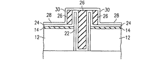
図1は、テトラエチルオキシレンの分解によって形成された酸化物(TEOS酸化物)またはBPSG(boron phosphate silicateglass)等の絶縁材料から成り得るメモリセル平坦化層12を示しており、この平坦化層12はこの層の上に被着された比較的薄いエッチングストップ層14及びこのエッチングストップ層14の上に被着された比較的厚いハードマスク層16を有している。ハードマスク層16は第1のサクリファイス層(first sacrificial layer)である。エッチングストップ層14及びハードマスク層16は、スパッタリングまたは化学的気相成長(CVD:chemical vapor deposition)プロセスを用いて被着することができる。エッチングストップ層14は、ハードマスク層16をエッチングするときのエッチングストップとして用いられる。エッチングストップ層14はSi3N4を含んだ種々の絶縁材料から成り得るのに対し、ハードマスク層16は酸化物(例えば、ドープトまたはノンドープトSiO2),TiN及びSOG(spun−on−glass)を含む種々のマスク材料から成り得る。図1ないし図6に示す典型的多クラウン記憶コンデンサ及び形成方法論に対して、エッチングストップ層14はSi3N4から成り、ハードマスク層16はTEOS酸化物から成っている。
【0014】
図2に示すように記憶ノードビア18をパターニング形成して、半導体層10内にコンタクトを露出させる。略円筒状断面のビア18は、自己整合式セルの形成後に記憶ノード(SN:storage node)形状にフィットさせるために、平坦化層,エッチングストップ層及びハードマスク層の種々の高さに応じた変化する高さを有する。ハードマスク層16及びエッチングストップ層14の組み合わされた厚さは、所望する記憶セルのクラウンの高さに応じて決定される。多クラウン記憶セル形成パラメータの1つの典型的なセットを表1にまとめてある。
【0015】
【表1】

普通の丸いビアと比較して本発明の低減されたビアの幅のために、自已整合式ビアエッチング段階を好ましくは用いるべきである。導電層のエッチングは記憶ノードを形成しこれを分離するために、この自己整合式SNエッチングは何らの付加的なフォトパターニング段階を要求するものではない。
【0017】
ビア18をパターニングして異方性エッチングを行った後、インシトゥーPドープト(ISD:in−situ P−doped)ポリシリコン等の導電性材料をビア18の内表面及びハードマスク層16の表面上に被着して、図3に示すように第1の導電層20を形成する。第1の導電層20は、図3に示すように、ビア18の側壁を覆ってビア18内に延びている。多クラウン記憶セル構造を形成すべく本発明のプロセスによって説明された各連続する導電層は、CVDまたはプラズマCVD成膜プロセスの何れかを用いて被着されたISDポリシリコンから成り得る。
【0018】
図4に示すように適切なエッチングによって第1の導電層20をエッチバックして、導電層20をビア18の垂直な側壁上に残すようにする。次に、図5に示すように、ハードマスク層16を除去するエッチングを行う。図3、図4及び図5に示すプロセス段階によって、記憶セルの第1のクラウン22及び第1のクラウン・ベース23が形成される。図5に示すように、第1のクラウン・ベース23はビア18領域内に形成され、一方、第1のクラウン22はビア18の上方に伸長する。第1のクラウン22は、第1のクラウン・ベース23からビア18の上方に伸長する略円筒状の伸長部を形成する。ビア18内に第1のクラウン・ベース23を形成することにより、第1のクラウン22には機械的安定性が与えられる。
【0019】
図6に示すように、露出したエッチングストップ層14,ビア18,第1のクラウン22の壁面及び第1のクラウン・ベース23に沿って第2の導電層24を被着して、ビア18の底部,第1のクラウン22及び第2のクラウン30の間にコンタクトをもたらすようにする。第2のサクリファイス層26即ちスペーサ層26を第2の導電層24上に成長させて、ビア18を充填して、連続的なクラウン間のスペーサとして機能するようにする。このスペーサ層26は、CVDまたはプラズマCVD成膜プロセスを用いて被着されたドープトまたはノンドープトSiO2から成り得る。次いで、スペーサ層26をエッチバックして、図8に示すように特定の領域の第2の導電層24及びスペーサ層26を露出させる。
【0020】
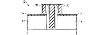
次いで、図9に示すように、スペーサ層26及び第2の導電層24の露出部分に沿って第3の導電層28を被着して、第2のクラウン30を形成する。次いで、エッチバック・プロセスを図9の構造に適用して、記憶セルの上面に関連する第3の導電層28及び記憶セル間に関連する底部の導電層(ポリシリコン)をエッチング除去して、図10に示すような第2のクラウン30及び多クラウン記憶セル10を形成する。次に、残存する酸化物スペーサ層26をエッチバックして、図11に示すように、本発明の教示による自己整合式ダブルクラウン記憶セル構造10をもたらす。代替実施例において、導電層エッチバック・プロセスは、スペーサ層26及び第2の導電層24が露出されるまで第3の導電層28について行うことができる。次いで、酸化物スペーサ層26をエッチバックすることができ、引き続き、第2の導電層24のエッチバック及び残存するエッチングストップ層14の除去を行って、ダブルクラウン記憶セル構造10をもたらす。図6ないし図11に説明したプロセスを多数回繰り返して、付加的クラウンを成長させることができる。
【0021】
第1のクラウン22と同様に、第3の導電層28は、ビア18の上方に第2のクラウン30を、またビア18内に第2のクラウン・ベース33を形成する。第2のクラウン30は第1のクラウン22の回りを取り囲んで形成されると共に、スペーサ26によって規定される距離だけ第1のクラウン22から離隔している。第2のクラウン・ベース33はビア18内に形成されて、製造の際及び製造の後の双方にて第2のクラウン30の機械的安定性を高める構造をもたらす。
【0022】
図11の実施例の製造されたダブルクラウン記憶セル構造10は、この自己整合式ダブルクラウン記憶セル10が1つのビア及び1つのSNパターンを有するこれまで提案された記憶セルに比して小さいセル分離を有するので、これまで開発された256M記憶セルに比して大きなセル寸法を有する。例えば、図11のダブルクラウン記憶セル10の全表面積は、0.5μmのSN高さにて簡易なスタック型セル(STC:stacked cell)の寸法の略3.2倍であり得る。
【0023】
一実施例において、各導電層をエッチングするのに使用される導電層エッチバック・プロセスは、各ポリシリコン層の表面を粗くして、平滑なダブルクラウン・セルと比較してダブルクラウン記憶セル10の表面積を増大すべく、AMATP−5000エッチャーを使用することを含み得る。更に、多クラウン記憶セル10の全表面積をより小さなビア及びより幅の狭いスペーサを使用することによって増大してトリプルクラウンセルを形成するとすれば、または導電層(例えば、ポリシリコン)エッチング・プロセスによってダブルクラウンセルに関連してでこぼこしたポリシリコン表面が得られれば、この自己整合式多クラウン記憶セル10の使用を1Gb DRAMに拡張することができる。本発明の記憶セル構造は、適切な誘電体の成膜及び上部プレートの形成に基づいて多クラウン型コンデンサを形成するものである。
【0024】
図12は、本発明の2つのダブルクラウン記憶セル構造実施例を組み込れたDRAMセルを示している。図12において、メモリセル平坦化層12は、トランジスタ対が形成された半導体基板100上に形成されている。各トランジスタは、ドレイン領域160及び接続されたビット線200を共有しながら、ソース領域140及びゲート電極180を有している。ビット線200及びドレイン領域160は、フィールド酸化物120によってアクティブ領域及び素子分離領域に分割された半導体基板100のアクティブ領域上に形成されている。絶縁層190を得られた構造体の全表面に渡って形成して、トランジスタ同士を絶縁することができる。平坦化層12は絶縁層190の機能を果たすことができる。次いで、図1ないし図11及び関連する本文で説明したプロセスによって、得られた構造体上に多クラウン記憶セル構造10を形成する。トランジスタは記憶ノード・コンタクトをビット線200に結合している。O/N/Oなどの誘電体材料210が、多クラウン記憶セル構造10の全表面上に被着される。不純物がドープされたポリシリコン等の上部プレート材料が誘電体材料210上に被着されて、上部プレート220を形成する。得られたDRAMセル構造は2つのダブルクラウン記憶コンデンサ240,250を組み込んでいる。
【0025】
要約すると、本発明は、半導体メモリデバイスに使用される自己整合式多クラウン記憶セル構造及びその製造方法を提供して、容量が増大した記憶コンデンサをもたらすものである。一実施例において、積層された平坦化絶縁層/エッチングストップ層/ハードマスク層中にコンクタト・ビアをパターニング形成し、第1の導電層を被着し、該第1の導電層をエッチングし、前記ハードマスク層をエッチングし、前記導電層がコートされパターニング形成されたビア及び前記エッチングストップ層上に第2の導電層を被着し、該第2の導電層上に酸化物層を被着し、該酸化物層をエッチングし、第3の導電層を被着し、(ポリシリコン等の)導電層材料をエッチンク化て前記エッチングストップ層を露出させ、かつ残りの酸化物層をエッチングすることによって、ダブルクラウン記憶セル構造を形成することができる。最後の幾つかの段階を繰り返して、3つ以上のクラウンを有する記憶セル構造を形成することができる。本発明の自己整合式多クラウン記憶セルは、所定のメモリアレイ表面領域内にて、増大した記憶セル表面積及び増大した電荷蓄積容量をもたらすものである。本発明の製造方法論は、フォトパターンレベルを除去すると共に、一層ロバストな製造プロセス及び機械的安定性が増大した記憶セルをもたらす。
【0026】
以上、本発明を詳細に説明したが、特許請求の範囲によって述べられるこの発明の精神及び範囲にもとること無く、種々の修正、変換及び変更を行い得ることを了知すべきである。
【0027】
以上の説明に関して更に以下の項を開示する。
【0028】
(1)ベース層と、
該ベース層内に形成されたビアと、
該ビア内に形成された第1のクラウン・ベース、及び、該第1のクラウン・ベースに隣接すると共に前記ビアの上方に略円筒状の伸長部を形成する第1のクラウンを備えた第1の導電層と、
前記ビア内に形成されると共に前記第1のクラウン・ベースを覆う少なくとも1つの周囲クラウン・ベース、及び、前記少なくとも1つの周囲クラウン・ベースに接続されると共に前記第1のクラウンから離隔して該第1のクラウンを取り囲む前記ベース層の上部の略円筒状の伸長部を形成する少なくとも1つの周囲クラウンを備えた少なくとも1つの周囲導電層と、を具備した半導体記憶セル構造。
【0029】
(2)前記少なくとも1つの周囲導電層が、前記ビア内に形成されると共に前記第1のクラウン・ベースを覆う第2のクラウン・ベース、及び、該第2のクラウン・ベースに接続されると共に前記第1のクラウンから離隔して該第1のクラウンを取り囲む前記ベース層の上部の略円筒状の伸長部を形成する第2のクラウンを備えた第2の導電層を含む、第1項記載の記憶セル構造。
【0030】
(3)前記少なくとも1つの周囲導電層が第2の導電層及び第3の導電層を含み、
第2の導電層が、
前記ビア内に形成されると共に、前記第1のクラウン・ベースを覆う第2のクラウン・ベースと、
該第2のクラウン・ベースに接続されると共に、前記第1のクラウンから離隔して該第1のクラウンを取り囲む前記ベース層の上部の略円筒状の伸長部を形成する第2のクラウンと、を備え、
前記第3の導電層が、
前記ビア内に形成されると共に、前記第2のクラウン・ベースを覆う第3のクラウン・ベースと、
該第3のクラウン・ベースに接続されると共に、前記第2のクラウンから離隔して該第2のクラウンを取り囲む前記ベース層の上部の略円筒状の伸長部を形成する第3のクラウンと、を備えた、第1項記載の記憶セル構造。
【0031】
(4)前記第1のクラウン及び前記第1のクラウン・ベースが、
積層された平坦化絶縁層/エッチング・ストップ層/ハードマスク層中にコンタクト・ビアをパターニング形成し、
前記パターニング形成されたビア及び前記ハードマスク層上に第1の導電層を被着し、
該第1の導電層をエッチングして前記ハードマスク層を露出させ、
該ハードマスク層をエッチングして前記エッチングストップ層を露出させる、ことによって形成される、第1項記載の記憶セル構造。
【0032】
(5)前記ベース層は酸化物で形成された絶縁層を備えた第1項記載の記憶セル構造。
【0033】
(6)各導電層はポリシリコンを備えた第1項記載の記憶セル構造。
【0034】
(7)各導電層は化学的気相成長法を用いて被着されたポリシリコンを備えた第1項記載の記憶セル構造。
【0035】
(8)多数のクラウン上に被着された誘電体と、
該誘電体及び前記記憶セル構造に渡って被着されて多クラウン記憶コンデンサを形成する上部プレート層と、を更に具備した第1項記載の記憶セル構造。
【0036】
(9)半導体メモリデバイスに使用する自己整合式多クラウン記憶セルの形成方法において、
平坦化されたベース層を設ける段階と、
該ベース層中にコンタクト・ビアをパターニング形成する段階と、
前記ベース層上に第1のサクリファイス層を形成する段階と、
前記パターニング形成したビア及び前記第1のサクリファイス層上に第1の導電層を被着する段階と、
該第1の導電層をエッチングして前記第1のサクリファイス層を露出させる段階と、
該第1のサクリファイス層を除去する段階と、
前記導電性材料でコートされパターニング形成されたビア上及び前記ベース層上に第2の導電層を被着する段階と、
該第2の導電層上に第2のサクリファイス層を被着して前記ビアを充填する段階と、
前記第2のサクリファイス層をエッチングして前記第2の導電層の一部分を露出させる段階と、
該第2の導電層の露出された部分及び残存する前記第2のサクリファイス層上に第3の導電層を被着する段階と、
前記導電層のエッチングを行って前記ベース層の一部分を露出させる段階と、
前記第2のサクリファイス層の残存する部分を除去してダブルクラウン記憶セル構造を形成する段階と、を具備する方法。
【0037】
(10)前記第1のサクリファイス層及び前記第2のサクリファイス層の双方は酸化物を備えた第9項記載の方法。
【0038】
(11)前記ベース層はエッチングストップ層を更に備えた第9項記載の方法。
【0039】
(12)前記導電性材料でコートされパターニング形成されたビア及び前記ベース層上に第4の導電層を被着する段階と、
該第4の導電層上に第3のサクリファイス層を被着する段階と、
該第3のサクリファイス層をエッチングして前記第4の導電層の一部分を露出させる段階と、
該第4の導電層の露出された部分及び残存する前記第3のサクリファイス層上に第5の導電層を被着する段階と、
エッチングを行って前記ベース層を露出させる段階と、
残存する前記第3のサクリファイス層をエッチングすることによって、3つのクラウンを有する記憶セル構造を形成する段階と、を更に具備した第9項記載の方法。
【0040】
(13)前記導電性材料でコートされパターニング形成されたビア及び前記ベース層上に第4の導電層を被着する段階と、
該第4の導電層上に第4のサクリファイス層を被着する段階と、
該第4のサクリファイス層をエッチンク化て前記第4の導電層の一部分を露出させる段階と、
該第4の導電層の露出部分及び残存する前記第4のサクリファイス層上に第5の導電層を被着する段階と、
導電性材料をエッチングして前記ベース層を露出させる段階と、
前記残存する第4のサクリファイス層をエッチングする段階と、
前記導電性材料でコートされパターニング形成されたビア及び前記エッチングストップ層上に第6の導電層を被着する段階と、
該第6の導電層上に第5のサクリファイス層を被着する段階と、
該第5のサクリファイス層をエッチングして前記第6の導電層の一部分を露出させる段階と、
該第6の導電層の露出部分及び残存する前記第5のサクリファイス層上に第7の導電層を被着する段階と、
導電性材料をエッチングして前記ベース層を露出させる段階と、
前記残存する第5のサクリファイス層をエッチングすることにより4つのクラウンを有する記憶セル構造を形成する段階と、を更に具備した第9項記載の前記方法。
【0041】
(14)前記導電性材料をエッチングして前記ベース層を露出させる段階が、
前記第3の導電層をエッチングして、残存する前記第2のサクリファイス層及び前記第2の導電層の一部分を露出させる段階と、
前記第2の導電層の露出部分をエッチングして、前記ベース層を露出させる段階と、を更に備えた第9項記載の方法。
【0042】
(15)前記ベース層は酸化物から形成された絶縁層及び該絶縁層上に被着されたSi3N4を含むエッチングストップ層を更に備えた第9項記載の方法。
【0043】
(16)各導電層は化学的気相成長法を用いて被着されたポリシリコンを含む第9項記載の方法。
【0044】
(17)前記第2のサクリファイス層は化学的気相成長法を用いて被着されたSiO2を含む第9項記載の方法。
【0045】
(18)前記記憶セル構造上に誘電体を被着する段階と、該誘電体一面に上部プレートを被着して多クラウン記憶コンデンサを形成する段階と、を更に具備した第9項記載の方法。
【0046】
(19)半導体メモリデバイスに使用する多クラウン記憶コンデンサにおいて、
酸化物から形成された平坦化絶縁層を備えたベース層と、
該ベース層内に形成されたビアと、
該ビア内に形成された第1のクラウン・ベース、及び、該第1のクラウン・ベースに隣接すると共に前記ビアの上方に略円筒状の伸長部を形成する第1のクラウンを備えた第1のドープト導電層と、
前記ビア内に形成されると共に前記第1のクラウン・ベースを覆う第2のクラウン・ベース、及び、該第2のクラウン・ベースに接続されると共に前記第1のクラウンから離隔して該第1のクラウンを取り囲む前記ベース層の上部の略円筒状の伸長部を形成する第2の周囲クラウンを備えた第2のドープト導電層と、
前記クラウンの各表面及び前記クラウン・ベースの各表面上に被着された誘電体と、
該誘電体を覆ってダブルクラウン記憶コンデンサを形成する上部プレートと、を具備した多クラウン記憶コンデンサ。
【0047】
(20)前記ビア内に形成されると共に前記第2のクラウン・ベースを覆う第3のクラウン・ベース、及び、該第3のクラウン・ベースに接続されると共に前記第2のクラウンから離隔して該第2のクラウンを取り囲む前記ベース層の上部の略円筒形の伸長部を形成する第3の周囲クラウンを備えた第3のPドープト導電層と、
前記第3のクラウン及び前記第3のクラウン・ベース上に被着されて、トリプルクラウン記憶コンデンサを形成する誘電体と、を更に具備した第19項記載の多クラウン記憶コンデンサ。
【0048】
(21)半導体層と、
該半導体層の表面に設けられると共に、第1及び第2のソース/ドレイン領域及びゲートを備えたトランジスタと、
前記第1のソース/ドレイン領域に電気的に結合されたビット線と、
メモリデバイス一面に設けられると共に、前記第2のソース/ドレイン領域上にビアを含む絶縁領域と、
前記第2のソース/ドレイン領域と接触する記憶ノード構造体であって、前記ビアの内壁に沿って形成されると共に、該ビアから離隔して前記絶縁領域を超えて伸長する第1のクラウン、及び、前記絶縁領域から離隔すると共に前記第1のクラウンから距離を置いて伸長する第2のクラウンを備えた前記記憶ノード構造体と、
該記憶ノード構造体一面に形成された誘電体層と、
該誘電体層一面に形成された上部プレート層と、を具備したメモリデバイス。
【0049】
(22)前記記憶ノード領域が、前記絶縁領域から離隔すると共に前記第2のクラウンから距離を置いて伸長する第3のクラウンを更に備えた第21項記載のメモリデバイス。
【0050】
(23)前記記憶ノード構造体が、前記絶縁領域から離隔して伸長する複数の付加的なクラウンを更に備え、各クラウンが他の全てのクラウンから距離を置いている、第21項記載のメモリデバイス。
【0051】
(24)前記各クラウンが導電性材料を含む第21項記載のメモリデバイス。
【0052】
(25)前記各クラウンがポリシリコンを含む第21項記載のメモリデバイス。
【0053】
(26)容量が増大した記憶コンデンサをもたらす、半導体メモリデバイスに使用する自己整合式多クラウン記憶セル構造10及びその製造方法。ダブルクラウン記憶セル構造実施例10は、絶縁層12,エッチングストップ層14及びハードマスク層16を含み得る平坦化ベース層にコンタクト・ビア18をパターニング形成し、第1の導電層20を被着し、第1の導電層20をエッチングし、ハードマスク層16をエッチングし、導電性材料でコートされパターニング形成されたビア18及びエッチングストップ層14上に第2の導電層24を被着し、第2の導電層24上にサクリファイス(酸化物)層26を被着し、サクリファイス層26をエッチングし、第3の導電層28を被着し、かつ導電性材料及び残存するサクリファイス層26をエッチングすることによって形成することができる。最後の幾つかの段階を繰り返して、3つ以上のクラウンを有する記憶セル構造10を形成することができる。
【図面の簡単な説明】
【図1】絶縁層上に積層されたエッチングストップ層/ハードマスク層の平面的な被着状態を示す断面図である。
【図2】図1の積層された絶縁層/エッチングストップ層/ハードマスク層内のビア領域の形成を示す断面図である。
【図3】図2のビアを有する構造内に記憶ノードをパターン形成すべく導電層を被着した状態を示す断面図である。
【図4】導電性材料をエッチングした後の図3の構造を示す断面図である。
【図5】ハードマスクをエッチングして、本発明による多クラウン記憶セルの第1のクラウンを形成した後の図4の構造を示す断面図である。
【図6】図5の構造一面に第2の導電層を成長させた状態を示す断面図である。
【図7】図6の構造上に酸化物層を被着した状態を示す断面図である。
【図8】酸化物層をエッチングした後の図7の構造を示す断面図である。
【図9】図8の構造上に導電層を被着形成した状態を示す断面図である。
【図10】導電性材料をエッチングした後の図9の構造を示す断面図である。
【図11】酸化物を選択的にエッチングして、本発明による多クラウン記憶セルの一実施例を得た状態を示す断面図である。
【図12】本発明の教示によって2つのダブルクラウン記憶コンデンサを組み込んだDRAMセルを示す断面図である。
【符号の説明】
10 多クラウン記憶セル
12 平坦化層
14 エッチングストップ層
16 ハードマスク層
18 ビア
20 第1の導電層
22 第1のクラウン
23 第1のクラウン・ベース
24 第2の導電層
26 第2のサクリファイス層(スペーサ層)
28 第3の導電層
30 第2のクラウン
33 第2のクラウン・ベース
100 半導体基板
120 フィールド酸化物
140 ソース領域
160 ドレイン領域
180 ゲート電極
200 ビット線
210 誘電体材料
220 上部プレート[0001]
BACKGROUND OF THE INVENTION
The present invention relates generally to semiconductor devices and methods for manufacturing the same, and more particularly to self-aligned multi-crown memory cells for use in memory devices and methods for manufacturing the self-aligned multi-crown memory cells.
[0002]
[Prior art and problems]
Reducing the size of semiconductor devices is a generally desirable goal in semiconductor manufacturing. This is true for semiconductor memory devices such as Dynamic Random Access Memory (DRAM). As the dimensions of semiconductor memory devices continue to shrink and the corresponding integration density continues to increase according to the 4x rule, the storage cells required become smaller while the required stored charge remains substantially the same. Conventional oxynitride (N / O or O / N / O) dielectrics have a relatively low capacitance per unit area (4.5 nm effective oxide) that limits storage capacity due to potential high tunnel leakage. About 7.7 fF / μm with respect to thickness 2 )have. To address this problem, various area enhancement techniques have been proposed, including hemispherical grain (HSG) bumpy poly, disc, fin and corrugated cylindrical cell (CCC). . However, these area enhancement techniques have inherent limitations.
[0003]
HSG technology requires complex deposition processes within a narrow temperature window. Memory cells incorporating fins, disks and CCC formation are primarily composed of a number of horizontal fins. As the size of the memory cell is further reduced, the fin adds less surface area than the vertical sidewall. Furthermore, the manufacture of typical fin-type structures is not a robust manufacturing process, which allows the memory cell to be mechanically stable, especially during horizontal fin-to-fin oxide removal and particulate removal. Will be lacking.
[0004]
In another attempt to overcome the limitations of conventional oxynitride dielectrics, Ta 2 O 5 , Ba 1-x Sr x TiO 3 (BST), SrTiO 3 And Pb 1-x Zr x TiO 3 High dielectric constant materials including (PZT) have been proposed as storage dielectrics due to their high capacitance per unit area. The high capacity per unit area is theoretically acceptable for the use of a simple stacked storage cell structure. However, high-k materials are new to semiconductor manufacturing, and there are several obstacles including transistor contamination, development of robust deposition processes, etching of new materials, integration experience and reliability. Exists for the implementation of semiconductor manufacturing.
[0005]
[Means for Solving the Problems]
The present invention provides a semiconductor memory device storage cell system and method for manufacturing the same that substantially eliminates or reduces disadvantages and problems associated with conventional storage cell systems and methods.
[0006]
More particularly, the present invention provides a self-aligned multi-crown memory cell structure for use in a semiconductor memory device and a method of manufacturing the self-aligned multi-crown memory cell resulting in a storage capacitor having increased capacitance. It is. One embodiment of the memory cell structure can be formed by patterning contact vias in the stacked planarization insulating layer / etch stop layer / hard mask layer and depositing a first conductive layer. . The first conductive layer and the hard mask layer are etched to form a first crown and an associated first crown base. A second conductive layer is deposited on the via and the etching stop layer coated and patterned with the conductive material, and an oxide layer is deposited on the second conductive layer. The oxide layer is etched to deposit a third conductive layer. The conductive material can be etched to expose the etch stop layer and the remaining oxide layer is etched to form the second crown in the double crown embodiment of the memory cell structure.
[0007]
A second conductive layer is deposited on the via and the etching stop layer coated and patterned with the conductive material, an oxide layer is deposited on the second conductive layer, and the oxide layer is Etching, depositing a third conductive layer, etching the third conductive layer to expose the etch stop layer, and repeating the steps of etching the remaining oxide layer to provide additional A crown can be formed to provide a memory cell structure with three or more crowns formed.
[0008]
The self-aligned semiconductor memory cell of the present invention provides the technical advantage of increased surface area by forming multiple crowns during the manufacturing process. By increasing the surface area, the storage capacity can be increased compared to a conventional storage cell of comparable dimensions.
[0009]
The present invention provides several manufacturing advantages. By using via formation, the multi-crown formation of the memory cell is truly self-aligned, thereby eliminating one photomask step in the formation of the memory cell. The simplified process flow of forming each crown from the first via helps the polysilicon via formation. The manufacturing process of the present invention is also compatible with a simple crown process and bumpy poly formation process. These manufacturing advantages reduce the complexity and cost of manufacturing the storage cell.
[0010]
A multi-crown memory cell formed in accordance with the teachings of the present invention incorporates a structure having a crown base for each crown contained within the via. This structure provides improved mechanical stability both during manufacture and upon final formation. This structure can also be easily expanded to increase the number of crowns in a relatively small cell structure.
[0011]
DETAILED DESCRIPTION OF THE INVENTION
The self-aligned multi-crown memory cell of the present invention is formed using a dielectric used in semiconductor devices including 256 Mb and 1 Gb DRAMs. Multi-crown memory cells are N / O, O / N / O, Ta as well as other relatively high dielectric constant materials. 2 O 5 , BST, and PZT. The multi-crown storage cell structure formation methodology of the present invention enables the formation of self-aligned storage cells of defined dimensions while eliminating one photo patterning (SN patterning) step. The present invention provides a memory cell structure having a more robust memory cell formation process and excellent mechanical stability.
[0012]
1-11 illustrate a self-aligned multi-crown memory cell formation process for a double crown memory cell structure. However, it should be appreciated that the formation methodology of the present invention can provide a memory cell having more than two crowns. By reducing via dimensions, polysilicon thickness, and crown spacing, a multi-crown storage cell can be constructed in which more than two crowns are formed within substantially the same memory array surface area. It is further understood that the self-aligned memory cell fabrication process of the present invention can be used to form a single crown cell by changing the process flow to eliminate the storage node (SN) patterning step. You should know.
[0013]
FIG. 1 shows a memory
[0014]
As shown in FIG. 2, the storage node via 18 is formed by patterning to expose the contact in the
[0015]
[Table 1]
A self-aligned via etch step should preferably be used because of the reduced via width of the present invention compared to ordinary round vias. This self-aligned SN etch does not require any additional photo-patterning steps in order for the etching of the conductive layer to form and isolate the storage node.
[0017]
After the via 18 is patterned and anisotropic etching is performed, a conductive material such as in-situ P-doped (ISD) polysilicon is applied on the inner surface of the via 18 and the surface of the
[0018]
The first
[0019]
As shown in FIG. 6, a second
[0020]
Next, as shown in FIG. 9, a third
[0021]
Similar to the
[0022]
The fabricated double crown
[0023]
In one embodiment, the conductive layer etchback process used to etch each conductive layer roughens the surface of each polysilicon layer and double
[0024]
FIG. 12 shows a DRAM cell incorporating two embodiments of the double crown memory cell structure of the present invention. In FIG. 12, the memory
[0025]
In summary, the present invention provides a self-aligned multi-crown storage cell structure for use in semiconductor memory devices and a method for manufacturing the same to provide a storage capacitor with increased capacitance. In one embodiment, patterning vias in the planarized insulating layer / etch stop layer / hard mask layer, depositing a first conductive layer, etching the first conductive layer, Etching the hard mask layer, depositing a second conductive layer over the patterned via and the etching stop layer coated with the conductive layer, and depositing an oxide layer over the second conductive layer Etching the oxide layer, depositing a third conductive layer, etching the conductive layer material (such as polysilicon) to expose the etch stop layer, and etching the remaining oxide layer Thus, a double crown memory cell structure can be formed. The last few steps can be repeated to form a memory cell structure with more than two crowns. The self-aligned multi-crown storage cell of the present invention provides increased storage cell surface area and increased charge storage capacity within a given memory array surface area. The manufacturing methodology of the present invention eliminates photopattern levels and results in memory cells with a more robust manufacturing process and increased mechanical stability.
[0026]
While the invention has been described in detail above, it should be understood that various modifications, changes and changes may be made without departing from the spirit and scope of the invention as defined by the appended claims.
[0027]
The following items are further disclosed with respect to the above description.
[0028]
(1) a base layer;
Vias formed in the base layer;
A first crown base formed in the via, and a first crown adjacent to the first crown base and forming a substantially cylindrical extension above the via; A conductive layer of
At least one peripheral crown base formed in the via and covering the first crown base; and connected to the at least one peripheral crown base and spaced apart from the first crown; A semiconductor memory cell structure comprising: at least one peripheral conductive layer having at least one peripheral crown forming a substantially cylindrical extension on top of the base layer surrounding the first crown.
[0029]
(2) the at least one surrounding conductive layer is formed in the via and is connected to the second crown base and a second crown base covering the first crown base; A first conductive layer comprising a second crown spaced apart from the first crown and forming a generally cylindrical extension of the upper portion of the base layer surrounding the first crown. Memory cell structure.
[0030]
(3) the at least one surrounding conductive layer includes a second conductive layer and a third conductive layer;
The second conductive layer is
A second crown base formed in the via and covering the first crown base;
A second crown connected to the second crown base and spaced apart from the first crown and forming a generally cylindrical extension of the upper portion of the base layer surrounding the first crown; With
The third conductive layer comprises:
A third crown base formed in the via and covering the second crown base;
A third crown connected to the third crown base and spaced apart from the second crown and forming a generally cylindrical extension of the upper portion of the base layer surrounding the second crown; A memory cell structure according to claim 1, comprising:
[0031]
(4) The first crown and the first crown base are:
Patterning contact vias in the planarized insulating layer / etching stop layer / hard mask layer,
Depositing a first conductive layer on the patterned via and the hard mask layer;
Etching the first conductive layer to expose the hard mask layer;
The memory cell structure according to claim 1, wherein the memory cell structure is formed by etching the hard mask layer to expose the etching stop layer.
[0032]
(5) The memory cell structure according to (1), wherein the base layer includes an insulating layer made of an oxide.
[0033]
(6) The memory cell structure according to item 1, wherein each conductive layer includes polysilicon.
[0034]
(7) The memory cell structure according to item 1, wherein each conductive layer includes polysilicon deposited by chemical vapor deposition.
[0035]
(8) a dielectric deposited on a number of crowns;
The memory cell structure of claim 1 further comprising: an upper plate layer deposited over the dielectric and the memory cell structure to form a multi-crown memory capacitor.
[0036]
(9) In a method of forming a self-aligned multi-crown memory cell for use in a semiconductor memory device,
Providing a planarized base layer;
Patterning contact vias in the base layer;
Forming a first sacrificial layer on the base layer;
Depositing a first conductive layer on the patterned via and the first sacrificial layer;
Etching the first conductive layer to expose the first sacrificial layer;
Removing the first sacrificial layer;
Depositing a second conductive layer over the patterned and patterned via and coated with the conductive material, and over the base layer;
Depositing a second sacrificial layer on the second conductive layer and filling the via;
Etching the second sacrificial layer to expose a portion of the second conductive layer;
Depositing a third conductive layer over the exposed portion of the second conductive layer and the remaining second sacrificial layer;
Etching the conductive layer to expose a portion of the base layer;
Removing the remaining portion of the second sacrificial layer to form a double crown memory cell structure.
[0037]
(10) The method according to item 9, wherein both of the first sacrificial layer and the second sacrificial layer comprise an oxide.
[0038]
(11) The method according to item 9, wherein the base layer further includes an etching stop layer.
[0039]
(12) depositing a fourth conductive layer on the via and the base layer coated and patterned with the conductive material;
Depositing a third sacrificial layer on the fourth conductive layer;
Etching the third sacrificial layer to expose a portion of the fourth conductive layer;
Depositing a fifth conductive layer on the exposed portion of the fourth conductive layer and the remaining third sacrificial layer;
Etching to expose the base layer;
10. The method of claim 9, further comprising: forming a memory cell structure having three crowns by etching the remaining third sacrificial layer.
[0040]
(13) depositing a fourth conductive layer on the via and the base layer coated and patterned with the conductive material;
Depositing a fourth sacrificial layer on the fourth conductive layer;
Etching the fourth sacrificial layer to expose a portion of the fourth conductive layer;
Depositing a fifth conductive layer over the exposed portion of the fourth conductive layer and the remaining fourth sacrificial layer;
Etching the conductive material to expose the base layer;
Etching the remaining fourth sacrificial layer;
Depositing a sixth conductive layer over the via and the etch stop layer coated and patterned with the conductive material;
Depositing a fifth sacrificial layer on the sixth conductive layer;
Etching the fifth sacrificial layer to expose a portion of the sixth conductive layer;
Depositing a seventh conductive layer on the exposed portion of the sixth conductive layer and the remaining fifth sacrificial layer;
Etching the conductive material to expose the base layer;
10. The method of claim 9, further comprising the step of etching the remaining fifth sacrificial layer to form a memory cell structure having four crowns.
[0041]
(14) etching the conductive material to expose the base layer;
Etching the third conductive layer to expose the remaining second sacrificial layer and a portion of the second conductive layer;
10. The method of claim 9, further comprising: etching an exposed portion of the second conductive layer to expose the base layer.
[0042]
(15) The base layer is an insulating layer formed of an oxide and Si deposited on the insulating layer. 3 N 4 The method according to claim 9, further comprising an etching stop layer comprising:
[0043]
(16) A method according to item 9 wherein each conductive layer comprises polysilicon deposited using chemical vapor deposition.
[0044]
(17) The second sacrificial layer is formed of SiO deposited by chemical vapor deposition. 2 The method of Claim 9 containing.
[0045]
(18) The method according to claim 9, further comprising the steps of: depositing a dielectric on the memory cell structure; and depositing an upper plate over the dielectric to form a multi-crown memory capacitor. .
[0046]
(19) In a multi-crown storage capacitor used in a semiconductor memory device,
A base layer with a planarizing insulating layer formed from an oxide;
Vias formed in the base layer;
A first crown base formed in the via, and a first crown adjacent to the first crown base and forming a substantially cylindrical extension above the via; A doped conductive layer of
A second crown base formed in the via and covering the first crown base; and connected to the second crown base and spaced apart from the first crown A second doped conductive layer comprising a second peripheral crown forming a substantially cylindrical extension on top of the base layer surrounding the crown;
A dielectric deposited on each surface of the crown and each surface of the crown base;
A multi-crown storage capacitor comprising: an upper plate covering the dielectric to form a double crown storage capacitor.
[0047]
(20) A third crown base formed in the via and covering the second crown base, and connected to the third crown base and spaced apart from the second crown A third P-doped conductive layer with a third peripheral crown forming a substantially cylindrical extension on top of the base layer surrounding the second crown;
20. The multi-crown storage capacitor of claim 19, further comprising a dielectric deposited on the third crown and the third crown base to form a triple crown storage capacitor.
[0048]
(21) a semiconductor layer;
A transistor provided on a surface of the semiconductor layer and having first and second source / drain regions and a gate;
A bit line electrically coupled to the first source / drain region;
An insulating region provided over the memory device and including a via on the second source / drain region;
A storage node structure in contact with the second source / drain region, the first crown formed along an inner wall of the via and extending away from the via and beyond the insulating region; And the storage node structure comprising a second crown spaced from the insulating region and extending at a distance from the first crown;
A dielectric layer formed over the storage node structure;
And a top plate layer formed on the entire surface of the dielectric layer.
[0049]
(22) The memory device according to item 21, wherein the storage node region further includes a third crown that is separated from the insulating region and extends at a distance from the second crown.
[0050]
23. The memory of claim 21, wherein the storage node structure further comprises a plurality of additional crowns extending away from the insulating region, each crown being spaced from all other crowns. device.
[0051]
(24) The memory device according to item 21, wherein each crown includes a conductive material.
[0052]
(25) A memory device according to item 21, wherein each crown includes polysilicon.
[0053]
(26) A self-aligned multi-crown
[Brief description of the drawings]
FIG. 1 is a cross-sectional view showing a planar deposition state of an etching stop layer / hard mask layer laminated on an insulating layer.
2 is a cross-sectional view showing formation of a via region in the stacked insulating layer / etching stop layer / hard mask layer of FIG. 1;
FIG. 3 is a cross-sectional view showing a state in which a conductive layer is deposited to pattern a storage node in the structure having the via of FIG. 2;
4 is a cross-sectional view illustrating the structure of FIG. 3 after etching a conductive material.
5 is a cross-sectional view of the structure of FIG. 4 after etching a hard mask to form a first crown of a multi-crown memory cell according to the present invention.
6 is a cross-sectional view showing a state in which a second conductive layer is grown on the entire structure of FIG. 5;
7 is a cross-sectional view showing a state in which an oxide layer is deposited on the structure of FIG. 6;
8 is a cross-sectional view showing the structure of FIG. 7 after etching the oxide layer.
9 is a cross-sectional view showing a state in which a conductive layer is deposited on the structure of FIG.
10 is a cross-sectional view showing the structure of FIG. 9 after etching a conductive material.
FIG. 11 is a cross-sectional view showing a state in which an embodiment of a multi-crown memory cell according to the present invention is obtained by selectively etching an oxide.
FIG. 12 is a cross-sectional view of a DRAM cell incorporating two double crown storage capacitors in accordance with the teachings of the present invention.
[Explanation of symbols]
10 Multi-crown memory cell
12 Planarization layer
14 Etching stop layer
16 Hard mask layer
18 Beer
20 First conductive layer
22 First Crown
23 First Crown Base
24 Second conductive layer
26 Second sacrificial layer (spacer layer)
28 Third conductive layer
30 second crown
33 Second Crown Base
100 Semiconductor substrate
120 field oxide
140 Source area
160 Drain region
180 Gate electrode
200 bit line
210 Dielectric Material
220 Upper plate
Claims (2)
該ベース層内に形成されたビアと、
該ビア内に形成された第1のクラウン・ベース、及び、該第1のクラウン・ベースに隣接すると共に、前記ビアの上方に略円筒状の伸長部を形成する第1のクラウンを備えた第1の導電層と、
前記ビア内に形成されると共に、前記第1のクラウン・ベースを覆う少なくとも1つの周囲クラウン・ベース、及び、前記少なくとも1つの周囲クラウン・ベースに接続されると共に、前記第1のクラウンから離隔して該第1のクラウンを取り囲む前記ベース層の上部の略円筒状の伸長部を形成する少なくとも1つの周囲クラウンを備えた少なくとも1つの周囲導電層と、
を具備した半導体記憶セル構造。 A base layer comprising a planarization insulating layer and an etching stop layer formed on the planarization insulation layer;
Vias formed in the base layer;
A first crown base formed in the via; and a first crown adjacent to the first crown base and forming a substantially cylindrical extension above the via. 1 conductive layer;
At least one peripheral crown base formed in the via and covering the first crown base and connected to the at least one peripheral crown base and spaced apart from the first crown At least one surrounding conductive layer with at least one surrounding crown forming a generally cylindrical extension on top of the base layer surrounding the first crown;
A semiconductor memory cell structure comprising:
平坦化絶縁層及び該平坦化絶縁層上に形成されたエッチングストップ層からなるベース層を設ける段階と、
該ベース層上に第1のサクリファイス層を形成する段階と、
前記ベース層及び前記第1のサクリファイス層を貫通したコンタクト・ビアをパターニング形成する段階と、
前記パターニング形成したビア及び前記第1のサクリファイス層上に第1の導電層を被着する段階と、
該第1の導電層をエッチングして前記第1のサクリファイス層を露出させる段階と、
該第1のサクリファイス層を除去する段階と、
前記第1の導電層でコートされパターニング形成されたビア上及び前記ベース層上に第2の導電層を被着する段階と、
該第2の導電層上に第2のサクリファイス層を被着して前記ビアを充填する段階と、
前記第2のサクリファイス層をエッチングして前記第2の導電層の一部分を露出させる段階と、
該第2の導電層の露出された部分及び残存する前記第2のサクリファイス層上に第3の導電層を被着する段階と、
該第3の導電層のエッチングを行って前記ベース層の一部分を露出させる段階と、
前記第2のサクリファイス層の残存する部分を除去してダブルクラウン記憶セル構造を形成する段階と、
を具備する方法。In a method of forming a self-aligned multi-crown memory cell for use in a semiconductor memory device,
Providing a base layer comprising a planarization insulating layer and an etching stop layer formed on the planarization insulation layer;
Forming a first sacrificial layer on the base layer,
Patterning contact vias penetrating the base layer and the first sacrificial layer;
Depositing a first conductive layer on the patterned via and the first sacrificial layer;
Etching the first conductive layer to expose the first sacrificial layer;
Removing the first sacrificial layer;
Depositing a second conductive layer on the via coated and patterned with the first conductive layer and on the base layer;
Depositing a second sacrificial layer on the second conductive layer and filling the via;
Etching the second sacrificial layer to expose a portion of the second conductive layer;
Depositing a third conductive layer over the exposed portion of the second conductive layer and the remaining second sacrificial layer;
Etching the third conductive layer to expose a portion of the base layer;
Removing a remaining portion of the second sacrificial layer to form a double crown memory cell structure;
A method comprising:
Applications Claiming Priority (2)
| Application Number | Priority Date | Filing Date | Title |
|---|---|---|---|
| US3372296P | 1996-12-20 | 1996-12-20 | |
| US033722 | 1996-12-20 |
Publications (2)
| Publication Number | Publication Date |
|---|---|
| JPH10294438A JPH10294438A (en) | 1998-11-04 |
| JP4282101B2 true JP4282101B2 (en) | 2009-06-17 |
Family
ID=21872072
Family Applications (1)
| Application Number | Title | Priority Date | Filing Date |
|---|---|---|---|
| JP37018997A Expired - Lifetime JP4282101B2 (en) | 1996-12-20 | 1997-12-22 | Self-aligned multi-crown memory capacitor and manufacturing method thereof |
Country Status (6)
| Country | Link |
|---|---|
| US (1) | US5972769A (en) |
| EP (1) | EP0849741B1 (en) |
| JP (1) | JP4282101B2 (en) |
| KR (1) | KR100517577B1 (en) |
| DE (1) | DE69733055T2 (en) |
| TW (1) | TW391064B (en) |
Families Citing this family (22)
| Publication number | Priority date | Publication date | Assignee | Title |
|---|---|---|---|---|
| DE19640273C1 (en) * | 1996-09-30 | 1998-03-12 | Siemens Ag | Method for manufacturing barrier-free semiconductor memory devices |
| US5905280A (en) * | 1997-02-11 | 1999-05-18 | Micron Technology, Inc. | Capacitor structures, DRAM cell structures, methods of forming capacitors, methods of forming DRAM cells, and integrated circuits incorporating capacitor structures and DRAM cell structures |
| US6162681A (en) * | 1998-01-26 | 2000-12-19 | Texas Instruments - Acer Incorporated | DRAM cell with a fork-shaped capacitor |
| TW372365B (en) * | 1998-04-20 | 1999-10-21 | United Microelectronics Corp | Manufacturing method for capacitors of dynamic random access memory |
| JPH11330397A (en) * | 1998-05-20 | 1999-11-30 | Mitsubishi Electric Corp | Method for manufacturing semiconductor device |
| TW413932B (en) * | 1999-03-05 | 2000-12-01 | Nanya Plastics Corp | Manufacturing method of crown-type capacitor structure |
| TW415084B (en) * | 1999-03-05 | 2000-12-11 | Nanya Technology Corp | Fabrication method of crown-shaped capacitor structure |
| KR100311050B1 (en) * | 1999-12-14 | 2001-11-05 | 윤종용 | Method for manufacturing electrode of capacitor |
| US7112503B1 (en) * | 2000-08-31 | 2006-09-26 | Micron Technology, Inc. | Enhanced surface area capacitor fabrication methods |
| US6346455B1 (en) * | 2000-08-31 | 2002-02-12 | Micron Technology, Inc. | Method to form a corrugated structure for enhanced capacitance |
| TW567575B (en) * | 2001-03-29 | 2003-12-21 | Toshiba Corp | Fabrication method of semiconductor device and semiconductor device |
| US8158527B2 (en) * | 2001-04-20 | 2012-04-17 | Kabushiki Kaisha Toshiba | Semiconductor device fabrication method using multiple resist patterns |
| KR100408411B1 (en) * | 2001-06-01 | 2003-12-06 | 삼성전자주식회사 | Semiconductor memory device and method for fabricating the same |
| KR100449030B1 (en) * | 2002-01-24 | 2004-09-16 | 삼성전자주식회사 | Stack Capacitor and Method of Fabricating the Same |
| US7105065B2 (en) * | 2002-04-25 | 2006-09-12 | Micron Technology, Inc. | Metal layer forming methods and capacitor electrode forming methods |
| KR100450678B1 (en) * | 2002-07-10 | 2004-10-01 | 삼성전자주식회사 | Semiconductor memory device comprising two-story capacitor bottom electrode and method of manufacturing the same |
| JP2004040059A (en) | 2002-07-08 | 2004-02-05 | Fujitsu Ltd | Semiconductor storage device manufacturing method and semiconductor storage device |
| KR100448855B1 (en) * | 2002-07-18 | 2004-09-18 | 주식회사 하이닉스반도체 | Manufacturing method for semiconductor device |
| KR100456699B1 (en) * | 2002-10-04 | 2004-11-10 | 삼성전자주식회사 | Lower electrode contact structure over an underlying layer and method of forming thereof |
| US7440255B2 (en) * | 2003-07-21 | 2008-10-21 | Micron Technology, Inc. | Capacitor constructions and methods of forming |
| JP4800796B2 (en) * | 2005-04-14 | 2011-10-26 | エルピーダメモリ株式会社 | Capacitor manufacturing method |
| JP5806905B2 (en) * | 2011-09-30 | 2015-11-10 | 株式会社半導体エネルギー研究所 | Semiconductor device |
Family Cites Families (20)
| Publication number | Priority date | Publication date | Assignee | Title |
|---|---|---|---|---|
| JPH03174765A (en) * | 1989-09-19 | 1991-07-29 | Oki Electric Ind Co Ltd | Semiconductor memory device and manufacture thereof |
| KR940006587B1 (en) * | 1991-05-23 | 1994-07-22 | 삼성전자 주식회사 | Manufacturing method of capacitor of DRAM cell |
| US5266512A (en) * | 1991-10-23 | 1993-11-30 | Motorola, Inc. | Method for forming a nested surface capacitor |
| KR960005251B1 (en) * | 1992-10-29 | 1996-04-23 | 삼성전자주식회사 | Manufacturing Method of Semiconductor Memory Device |
| KR960015122B1 (en) * | 1993-04-08 | 1996-10-28 | 삼성전자 주식회사 | Manufacturing method of highly integrated semiconductor memory device |
| KR960011664B1 (en) * | 1993-05-21 | 1996-08-24 | 현대전자산업 주식회사 | Capacitor Formation Method of Semiconductor Device |
| JPH06338592A (en) * | 1993-05-31 | 1994-12-06 | Toshiba Corp | Semiconductor memory device and manufacture thereof |
| JP2555965B2 (en) * | 1993-12-13 | 1996-11-20 | 日本電気株式会社 | Method for manufacturing semiconductor device |
| KR0126799B1 (en) * | 1993-12-31 | 1997-12-29 | 김광호 | Capacitor Manufacturing Method of Semiconductor Device |
| US5521112A (en) * | 1994-10-05 | 1996-05-28 | Industrial Technology Research Institute | Method of making capacitor for stack dram cell |
| JP3374568B2 (en) * | 1995-01-09 | 2003-02-04 | ソニー株式会社 | Method for manufacturing semiconductor device |
| JP2682509B2 (en) * | 1995-04-28 | 1997-11-26 | 日本電気株式会社 | Method for manufacturing semiconductor device |
| US5550077A (en) * | 1995-05-05 | 1996-08-27 | Vanguard International Semiconductor Corporation | DRAM cell with a comb-type capacitor |
| US5789291A (en) * | 1995-08-07 | 1998-08-04 | Vanguard International Semiconductor Corporation | Dram cell capacitor fabrication method |
| US5550076A (en) * | 1995-09-11 | 1996-08-27 | Vanguard International Semiconductor Corp. | Method of manufacture of coaxial capacitor for dram memory cell and cell manufactured thereby |
| KR0171098B1 (en) * | 1995-12-19 | 1999-02-01 | 문정환 | Capacitor fabrication method |
| US5807775A (en) * | 1996-06-24 | 1998-09-15 | Vanguard International Semiconductor Corporation | Method for forming a double walled cylindrical capacitor for a DRAM |
| TW312831B (en) * | 1996-08-16 | 1997-08-11 | United Microelectronics Corp | Manufacturing method of semiconductor memory device with capacitor(3) |
| US5811331A (en) * | 1996-09-24 | 1998-09-22 | Taiwan Semiconductor Manufacturing Company Ltd. | Formation of a stacked cylindrical capacitor module in the DRAM technology |
| US5726086A (en) * | 1996-11-18 | 1998-03-10 | Mosel Vitelic Inc. | Method of making self-aligned cylindrical capacitor structure of stack DRAMS |
-
1997
- 1997-12-18 US US08/993,637 patent/US5972769A/en not_active Expired - Lifetime
- 1997-12-19 KR KR1019970070637A patent/KR100517577B1/en not_active Expired - Lifetime
- 1997-12-22 JP JP37018997A patent/JP4282101B2/en not_active Expired - Lifetime
- 1997-12-22 DE DE69733055T patent/DE69733055T2/en not_active Expired - Lifetime
- 1997-12-22 EP EP97310471A patent/EP0849741B1/en not_active Expired - Lifetime
-
1998
- 1998-07-17 TW TW087111629A patent/TW391064B/en not_active IP Right Cessation
Also Published As
| Publication number | Publication date |
|---|---|
| DE69733055D1 (en) | 2005-05-25 |
| EP0849741A2 (en) | 1998-06-24 |
| US5972769A (en) | 1999-10-26 |
| EP0849741B1 (en) | 2005-04-20 |
| DE69733055T2 (en) | 2006-03-09 |
| JPH10294438A (en) | 1998-11-04 |
| TW391064B (en) | 2000-05-21 |
| KR100517577B1 (en) | 2006-04-21 |
| EP0849741A3 (en) | 2001-10-04 |
| KR19980064364A (en) | 1998-10-07 |
Similar Documents
| Publication | Publication Date | Title |
|---|---|---|
| JP4282101B2 (en) | Self-aligned multi-crown memory capacitor and manufacturing method thereof | |
| US5491103A (en) | Method for manufacturing a capacitor structure of a semiconductor memory device | |
| US5162248A (en) | Optimized container stacked capacitor DRAM cell utilizing sacrificial oxide deposition and chemical mechanical polishing | |
| USRE36786E (en) | Process to manufacture crown stacked capacitor structures with HSG-rugged polysilicon on all sides of the storage node | |
| US5851876A (en) | Method of manufacturing dynamic random access memory | |
| US5270241A (en) | Optimized container stacked capacitor DRAM cell utilizing sacrificial oxide deposition and chemical mechanical polishing | |
| JP2617049B2 (en) | Method for manufacturing highly integrated semiconductor memory device | |
| JP3384599B2 (en) | Semiconductor device and manufacturing method thereof | |
| US5354705A (en) | Technique to fabricate a container structure with rough inner and outer surfaces | |
| US5994197A (en) | Method for manufacturing dynamic random access memory capable of increasing the storage capacity of the capacitor | |
| US20110186964A1 (en) | Methods of forming integrated circuit devices | |
| US6312986B1 (en) | Concentric container fin capacitor and method | |
| JP3222944B2 (en) | Method for manufacturing capacitor of DRAM cell | |
| US5438013A (en) | Method of making a semiconductor memory device having a capacitor | |
| US6294436B1 (en) | Method for fabrication of enlarged stacked capacitors using isotropic etching | |
| US6291850B1 (en) | Structure of cylindrical capacitor electrode with layer of hemispherical grain silicon | |
| US6097055A (en) | Capacitor and method for fabricating the same | |
| US5930621A (en) | Methods for forming vertical electrode structures and related structures | |
| US5663093A (en) | Method for forming a cylindrical capacitor having a central spine | |
| US5817554A (en) | Use of a grated top surface topography for capacitor structures | |
| US6011286A (en) | Double stair-like capacitor structure for a DRAM cell | |
| JPH0870100A (en) | Ferroelectric capacitor manufacturing method | |
| US5824582A (en) | Stack DRAM cell manufacturing process with high capacitance capacitor | |
| US6130126A (en) | Self-planarizing DRAM chip avoids edge flaking | |
| GB2276980A (en) | Semiconductor device stacked capacitor and method of manufacture |
Legal Events
| Date | Code | Title | Description |
|---|---|---|---|
| A621 | Written request for application examination |
Free format text: JAPANESE INTERMEDIATE CODE: A621 Effective date: 20041119 |
|
| A977 | Report on retrieval |
Free format text: JAPANESE INTERMEDIATE CODE: A971007 Effective date: 20070403 |
|
| A131 | Notification of reasons for refusal |
Free format text: JAPANESE INTERMEDIATE CODE: A131 Effective date: 20080111 |
|
| A601 | Written request for extension of time |
Free format text: JAPANESE INTERMEDIATE CODE: A601 Effective date: 20080411 |
|
| A602 | Written permission of extension of time |
Free format text: JAPANESE INTERMEDIATE CODE: A602 Effective date: 20080416 |
|
| A601 | Written request for extension of time |
Free format text: JAPANESE INTERMEDIATE CODE: A601 Effective date: 20080512 |
|
| A602 | Written permission of extension of time |
Free format text: JAPANESE INTERMEDIATE CODE: A602 Effective date: 20080515 |
|
| A601 | Written request for extension of time |
Free format text: JAPANESE INTERMEDIATE CODE: A601 Effective date: 20080611 |
|
| A602 | Written permission of extension of time |
Free format text: JAPANESE INTERMEDIATE CODE: A602 Effective date: 20080616 |
|
| A02 | Decision of refusal |
Free format text: JAPANESE INTERMEDIATE CODE: A02 Effective date: 20080912 |
|
| A521 | Request for written amendment filed |
Free format text: JAPANESE INTERMEDIATE CODE: A523 Effective date: 20081211 |
|
| A911 | Transfer to examiner for re-examination before appeal (zenchi) |
Free format text: JAPANESE INTERMEDIATE CODE: A911 Effective date: 20090120 |
|
| TRDD | Decision of grant or rejection written | ||
| A01 | Written decision to grant a patent or to grant a registration (utility model) |
Free format text: JAPANESE INTERMEDIATE CODE: A01 Effective date: 20090213 |
|
| A01 | Written decision to grant a patent or to grant a registration (utility model) |
Free format text: JAPANESE INTERMEDIATE CODE: A01 |
|
| A61 | First payment of annual fees (during grant procedure) |
Free format text: JAPANESE INTERMEDIATE CODE: A61 Effective date: 20090317 |
|
| R150 | Certificate of patent or registration of utility model |
Free format text: JAPANESE INTERMEDIATE CODE: R150 |
|
| FPAY | Renewal fee payment (event date is renewal date of database) |
Free format text: PAYMENT UNTIL: 20120327 Year of fee payment: 3 |
|
| FPAY | Renewal fee payment (event date is renewal date of database) |
Free format text: PAYMENT UNTIL: 20120327 Year of fee payment: 3 |
|
| FPAY | Renewal fee payment (event date is renewal date of database) |
Free format text: PAYMENT UNTIL: 20130327 Year of fee payment: 4 |
|
| FPAY | Renewal fee payment (event date is renewal date of database) |
Free format text: PAYMENT UNTIL: 20130327 Year of fee payment: 4 |
|
| FPAY | Renewal fee payment (event date is renewal date of database) |
Free format text: PAYMENT UNTIL: 20140327 Year of fee payment: 5 |
|
| R250 | Receipt of annual fees |
Free format text: JAPANESE INTERMEDIATE CODE: R250 |
|
| R250 | Receipt of annual fees |
Free format text: JAPANESE INTERMEDIATE CODE: R250 |
|
| R250 | Receipt of annual fees |
Free format text: JAPANESE INTERMEDIATE CODE: R250 |
|
| R250 | Receipt of annual fees |
Free format text: JAPANESE INTERMEDIATE CODE: R250 |
|
| EXPY | Cancellation because of completion of term |