JP2020126162A - Light guide plate for image display - Google Patents
Light guide plate for image display Download PDFInfo
- Publication number
- JP2020126162A JP2020126162A JP2019018945A JP2019018945A JP2020126162A JP 2020126162 A JP2020126162 A JP 2020126162A JP 2019018945 A JP2019018945 A JP 2019018945A JP 2019018945 A JP2019018945 A JP 2019018945A JP 2020126162 A JP2020126162 A JP 2020126162A
- Authority
- JP
- Japan
- Prior art keywords
- layer
- guide plate
- light guide
- image display
- image
- Prior art date
- Legal status (The legal status is an assumption and is not a legal conclusion. Google has not performed a legal analysis and makes no representation as to the accuracy of the status listed.)
- Pending
Links
Images



Landscapes
- Optical Filters (AREA)
- Diffracting Gratings Or Hologram Optical Elements (AREA)
- Laminated Bodies (AREA)
Abstract
【課題】画像表示用導光板において、透明材料の黄変による表示画像への影響を低減できるようにする。【解決手段】画像表示用導光板5は、樹脂基材1、ホログラム層2、および吸収層4を含む。吸収層4は、500nm以上600nm以下の波長範囲に吸収ピークを有する。【選択図】図1PROBLEM TO BE SOLVED: To reduce an influence on a displayed image due to yellowing of a transparent material in a light guide plate for image display. An image display light guide plate 5 includes a resin base material 1, a hologram layer 2, and an absorption layer 4. The absorption layer 4 has an absorption peak in a wavelength range of 500 nm or more and 600 nm or less. [Selection diagram] Fig. 1
Description
本発明は、画像表示用導光板に関する。 The present invention relates to a light guide plate for image display.
表示装置において、画像表示用導光板が用いられる場合がある。例えば、VR(仮想現実)技術、AR(拡張現実)技術、MR(複合現実)技術などを用いた表示装置においては、ホログラム層が透明基材に支持された画像表示用導光板が用いられる。ホログラム層には、種々の光学機能、例えば、導波、反射、回折などの機能を有するホログラムが形成される。
例えば、特許文献1には、光学接着剤を介して樹脂基体に挟まれたホログラムを有する積層体であって、外周部全体が保護被覆層で覆われたホログラム積層体が記載されている。さらに、特許文献1には、ホログラムで使用する波長の光は透過し、それより短い波長の光を吸収するいわゆる短波長カットフィルタを設けてもよいことが記載されている。
一方、ホログラム層を有する画像表示用導光板に関する技術ではないが、特許文献2には、レンズ用プラスチック材料の熱硬化時の黄変に起因するレンズの黄色度を改善する目的で、顔料の表面に疎水性シリカコーティングを施したプラスチック光学材料用ブルーイング剤をレンズ形成材料中に分散させることが提案されている。
An image display light guide plate may be used in a display device. For example, in a display device using VR (Virtual Reality) technology, AR (Augmented Reality) technology, MR (Mixed Reality) technology, and the like, an image display light guide plate having a hologram layer supported by a transparent substrate is used. Holograms having various optical functions such as waveguiding, reflection, and diffraction are formed on the hologram layer.
For example,
On the other hand, although it is not a technique relating to a light guide plate for image display having a hologram layer,
しかしながら、上記のような関連技術には、以下のような問題がある。
黄色は比視感度が高いため、画像表示用導光板においてホログラム層等の透明材料の黄変が生じると、画像を見る際にコントラスト(明暗度)が低くなってしまう。この結果、画像が不鮮明に見える。
特許文献1に記載の技術では、紫外光など画像表示用導光板の画像表示に用いない短波長光がカットされるので、紫外光に起因する画像表示用導光板に用いる樹脂材料の経時変化、例えば、透明度低下、着色など、を抑制できる。
しかし、ホログラム層を形成するフォトポリマー材料、および任意で設けられるバリア層などは、特に黄変しやすいので、製造直後であっても黄色味を帯びている。このため、特許文献1のように、短波長カットフィルタを設けても、製造直後から生じている黄色味は除去できないという問題がある。
これに対して、特許文献2に記載の技術をホログラム層に適用することも考えられる。しかし、特許文献1のブルーイング剤は、平均粒径が0.4μm〜0.6μm程度であるため、ホログラム層中にブルーイング剤を混ぜると、ホログラム層における干渉縞の記録に支障が生じるという問題がある。
However, the related art as described above has the following problems.
Since yellow has a high relative luminous efficiency, if the transparent material such as the hologram layer is yellowed in the image display light guide plate, the contrast (brightness) becomes low when the image is viewed. As a result, the image looks unclear.
In the technique described in
However, the photopolymer material forming the hologram layer, the optional barrier layer, and the like are particularly liable to yellow, so that they are yellowish even immediately after production. For this reason, there is a problem in that even if a short-wavelength cut filter is provided as in
On the other hand, it may be possible to apply the technique described in
本発明は、上記のような問題に鑑みてなされたものであり、透明材料の黄変による表示画像への影響を低減できる画像表示用導光板を提供することを目的とする。 The present invention has been made in view of the above problems, and an object of the present invention is to provide an image display light guide plate that can reduce the influence of yellowing of a transparent material on a displayed image.
上記の課題を解決するため、例えば、本発明は以下の態様を有する。
[1] 樹脂基材およびホログラム層を有する画像表示用導光板であって、500nm以上600nm以下の波長範囲に吸収ピークを有する吸収層を含むことを特徴とする画像表示用導光板。
[2] 前記吸収層、前記樹脂基材、および前記ホログラム層は、厚み方向においてこの順に配置されている、[1]の画像表示用導光板。
[3] 前記吸収層は、前記ホログラム層における表示画像出射部と厚み方向において重なる範囲に配置されている、[1]の画像表示用導光板。
[4] 前記吸収層は、前記樹脂基材の内部の少なくとも一部に色材が分散されて形成されている、[1]の画像表示用導光板。
[5] バリア層をさらに含む、[1]の画像表示用導光板。
[6] 前記バリア層は、前記樹脂基材と前記ホログラム層との間に配置されている、[5]の画像表示用導光板。
In order to solve the above problems, for example, the present invention has the following aspects.
[1] A light guide plate for image display having a resin base material and a hologram layer, which includes an absorption layer having an absorption peak in a wavelength range of 500 nm or more and 600 nm or less.
[2] The light guide plate for image display of [1], wherein the absorption layer, the resin base material, and the hologram layer are arranged in this order in the thickness direction.
[3] The light guide plate for image display according to [1], wherein the absorption layer is arranged in a range overlapping with a display image emission part in the hologram layer in the thickness direction.
[4] The light guide plate for image display according to [1], wherein the absorption layer is formed by dispersing a coloring material in at least a part of the inside of the resin base material.
[5] The light guide plate for image display according to [1], further including a barrier layer.
[6] The light guide plate for image display of [5], wherein the barrier layer is arranged between the resin base material and the hologram layer.
本発明によれば、透明材料の黄変による表示画像への影響を低減できる画像表示用導光板を提供できる。 ADVANTAGE OF THE INVENTION According to this invention, the light guide plate for image displays which can reduce the influence on the display image by yellowing of a transparent material can be provided.
以下では、本発明の実施形態について添付図面を参照して説明する。すべての図面において、実施形態が異なる場合であっても、同一または相当する部材には同一の符号を付し、共通する説明は省略する。 Embodiments of the present invention will be described below with reference to the accompanying drawings. In all the drawings, the same or corresponding members are denoted by the same reference numerals even if the embodiments are different, and common description is omitted.
本発明の実施形態の画像表示用導光板について説明する。
本実施形態の画像表示用導光板は、樹脂基材、ホログラム層、および吸収層を有する。
本実施形態の画像表示用導光板は、適宜の透明層をさらに有していてもよい。透明層の例としては、バリア層、接着層、ハードコート層、アンカーコート層などが含まれてもよい。
本実施形態の画像表示用導光板は、ガラス基材をさらに有していてもよい。
An image display light guide plate according to an embodiment of the present invention will be described.
The image display light guide plate of the present embodiment has a resin base material, a hologram layer, and an absorption layer.
The image display light guide plate of the present embodiment may further include an appropriate transparent layer. Examples of transparent layers may include barrier layers, adhesive layers, hard coat layers, anchor coat layers, and the like.
The image display light guide plate of the present embodiment may further include a glass base material.
画像表示用導光板は、画像光を入射する入射部と、画像光による画像を表示する表示画像出射部と、を有する。ホログラム層は、入射部と表示画像出射部との間に配置されている。ホログラム層には、少なくとも入射部から入射される画像光を表示画像出射部に導波し、表示画像出射部から出射させるための回折格子パターンが形成されている。表示画像出射部における回折格子パターンは、画像表示用導光板の外部から入射する外光の少なくとも一部を透過させる。
入射部から入射した画像光は、ホログラム層内に導波され、表示画像出射部から外部に出射される。一方、外光も樹脂基材および表示画像出射部を透過する結果、表示画像出射部の観察者は、画像光および外光の両方を、視野内で観察することができる。
本実施形態の画像表示用導光板は、VR技術、AR技術、MR技術を用いた表示装置などに好適に用いられる。例えば、本実施形態の画像表示用導光板は、ディスプレイ用途の他に、自動車搭載用のヘッドアップディスプレイ(HUD)のコンバイナや反射型液晶表示デバイス用の反射板に代表されるホログラム光学素子(HOE)などの装置に用いられてもよい。
The image display light guide plate includes an incident portion that makes image light incident, and a display image emitting portion that displays an image by the image light. The hologram layer is arranged between the incident portion and the display image emitting portion. The hologram layer is formed with a diffraction grating pattern for guiding at least the image light incident from the incident portion to the display image emitting portion and causing the image light to be emitted from the display image emitting portion. The diffraction grating pattern in the display image emitting portion transmits at least a part of external light incident from the outside of the image display light guide plate.
The image light incident from the incident portion is guided inside the hologram layer and emitted to the outside from the display image emitting portion. On the other hand, as a result of external light also passing through the resin base material and the display image emitting part, an observer of the display image emitting part can observe both the image light and the external light in the visual field.
The image display light guide plate of the present embodiment is preferably used for a display device using VR technology, AR technology, MR technology, and the like. For example, the image display light guide plate of the present embodiment is used for a display, as well as a hologram optical element (HOE) represented by a combiner of a head-up display (HUD) mounted on an automobile and a reflector of a reflective liquid crystal display device. ) Or the like.
樹脂基材の材料は、透明材料であれば特に限定されない。
樹脂基材に用いられる材料は、アクリル樹脂、環状ポリオレフィン樹脂、およびポリカーボネート樹脂からなる群から選ばれた1以上の樹脂を含有することがより好ましい。
The material of the resin base material is not particularly limited as long as it is a transparent material.
The material used for the resin substrate more preferably contains one or more resins selected from the group consisting of acrylic resins, cyclic polyolefin resins, and polycarbonate resins.
本実施形態の画像表示用導光板において、樹脂基材は、ホログラム層を間に挟んで2枚設けられてもよい。画像表示用導光板にガラス基材が含まれる場合、樹脂基材とガラス基材と間にホログラム層が配置されてもよい。
樹脂基材およびホログラム層、またはガラス基材およびホログラム層は、互いに接していてもよいし、それぞれの間に適宜の透明層が配置されてもよい。
In the image display light guide plate of the present embodiment, two resin base materials may be provided with the hologram layer interposed therebetween. When the image display light guide plate includes a glass base material, a hologram layer may be disposed between the resin base material and the glass base material.
The resin base material and the hologram layer, or the glass base material and the hologram layer may be in contact with each other, or an appropriate transparent layer may be arranged between them.
ホログラム層は、2枚の樹脂基材の間、または樹脂基材とガラス基材との間に、挟まれている。
ホログラム層は、周知のホログラム形成用樹脂材料が用いられる。例えば、ホログラム材料の例としては、具体的には、溶媒可溶性でカチオン重合可能なエチレンオキシド環を構造単位中に少なくともひとつ有する熱硬化性樹脂と、ラジカル重合可能なエチレン性モノマーよりなるホログラム記録材料(特開平8−1676、特開平8−1677、特開平8−1678、特開平8−1679)などが挙げられる。
The hologram layer is sandwiched between two resin base materials or between a resin base material and a glass base material.
A well-known hologram forming resin material is used for the hologram layer. For example, as an example of the hologram material, specifically, a hologram recording material composed of a thermosetting resin having at least one cationically polymerizable ethylene oxide ring in a structural unit and a radically polymerizable ethylenic monomer ( JP-A-8-1676, JP-A-8-1677, JP-A-8-1678, JP-A-8-1679) and the like can be mentioned.
吸収層は、画像表示用導光板の少なくとも一部を透過する光における黄色成分を吸収する波長特性を有する。
[吸収ピーク]
吸収層は、500nm以上600nm以下の波長範囲(以下、波長範囲A)に吸収ピークを有する。
ここで、「吸収ピーク」は、可視光域(400nm以上800nm以下)における吸収層の分光透過率曲線において透過率が減少から極小値を経て増大に転じるU字状の分光分布のうち、極小値が最小となる分光分布を指す。U字状の分光分布は可視光域において1箇所に形成されていることがより好ましい。
本明細書では、このような「吸収ピーク」の極小値(ピークトップ)を与える波長が特定の波長範囲にあることを、「特定の波長範囲に吸収ピークを有する」と定義する。
吸収ピークは、550nm以上585nm以下の波長範囲(以下、波長範囲B)にあることがより好ましい。
吸収ピークの半値幅は、100nm以下であってもよく、より好ましくは70nm以下、特に好ましくは40nm以下である。
ここで、吸収ピークの半値幅とは、吸収ピークのピークトップの透過率をTp(%)とするとき、透過率がTh=(100−Tp)/2以下となる吸収ピークの波長幅を意味する。
半値幅が100nm以下であると、透過光の色バランスと輝度とを良好に確保できる。
吸収ピークにおける透過率は、80%以下であってよく、より好ましくは70%以下、特に好ましくは60%以下である。
The absorption layer has a wavelength characteristic of absorbing the yellow component in the light transmitted through at least a part of the image display light guide plate.
[Absorption peak]
The absorption layer has an absorption peak in a wavelength range of 500 nm to 600 nm (hereinafter, wavelength range A).
Here, the “absorption peak” is the minimum value in the U-shaped spectral distribution in which the transmittance changes from a decrease to a minimum value and then to an increase in the spectral transmittance curve of the absorption layer in the visible light range (400 nm to 800 nm). Refers to the spectral distribution that minimizes. It is more preferable that the U-shaped spectral distribution is formed at one location in the visible light range.
In the present specification, a wavelength having a minimum value (peak top) of such an "absorption peak" in a specific wavelength range is defined as "having an absorption peak in a specific wavelength range".
The absorption peak is more preferably in the wavelength range of 550 nm to 585 nm (hereinafter, wavelength range B).
The full width at half maximum of the absorption peak may be 100 nm or less, more preferably 70 nm or less, and particularly preferably 40 nm or less.
Here, the full width at half maximum of the absorption peak means the wavelength width of the absorption peak at which the transmittance is Th=(100−Tp)/2 or less when the transmittance at the peak top of the absorption peak is Tp(%). To do.
When the full width at half maximum is 100 nm or less, the color balance and brightness of transmitted light can be well secured.
The transmittance at the absorption peak may be 80% or less, more preferably 70% or less, and particularly preferably 60% or less.
[透過率特性]
590nm以上700nm以下の波長範囲(以下、波長範囲C)における吸収層の平均透過率は、20%以上であってもよく、より好ましくは50%以上、さらに好ましくは70%以上である。
波長範囲Cにおいて、平均透過率が20%以上とするのは、赤色光の輝度を維持するためである。
470nm以上550nm以下の波長範囲(以下、波長範囲D)における吸収層の平均透過率は、20%以上であってもよく、より好ましくは50%以上、さらに好ましくは70%以上である。
波長範囲Dにおいて、平均透過率が20%以上とするのは、透過光の色バランスと輝度を確保するためである。
吸収層の透過率特性は、光劣化を起こしやすい紫外光の透過率が低いほどより好ましい。例えば380nm以下の波長範囲における吸収層の透過率は、5%以下であってもよく、より好ましくは3%以下、さらに好ましくは1%以下である。
[Transmittance characteristics]
The average transmittance of the absorption layer in the wavelength range of 590 nm to 700 nm (hereinafter, wavelength range C) may be 20% or more, more preferably 50% or more, and further preferably 70% or more.
The reason why the average transmittance is 20% or more in the wavelength range C is to maintain the brightness of red light.
The average transmittance of the absorption layer in the wavelength range of 470 nm or more and 550 nm or less (hereinafter, wavelength range D) may be 20% or more, more preferably 50% or more, and further preferably 70% or more.
The reason why the average transmittance is 20% or more in the wavelength range D is to ensure the color balance and brightness of the transmitted light.
Regarding the transmittance characteristics of the absorption layer, the lower the transmittance of ultraviolet light that is prone to photodegradation, the more preferable. For example, the transmittance of the absorption layer in the wavelength range of 380 nm or less may be 5% or less, more preferably 3% or less, and further preferably 1% or less.
[黄色度]
吸収層の黄色度を表すYI値(JIS K7373)は、10以下であってもよく、より好ましくは5以下、特に好ましくは3以下である。
[Yellowness]
The YI value (JIS K7373) representing the yellowness of the absorbing layer may be 10 or less, more preferably 5 or less, and particularly preferably 3 or less.
[吸光度]
吸収層の波長580nmにおける吸光度は、0.5以下であってもよく、より好ましくは0.3以下、特に好ましくは0.2以下である。
[Absorbance]
The absorbance of the absorption layer at a wavelength of 580 nm may be 0.5 or less, more preferably 0.3 or less, and particularly preferably 0.2 or less.
[L*a*b*表色系におけるb*]
吸収層のb*は、5以下であってもよく、より好ましくは3以下、特に好ましくは1以下である。
[L * a * b * b in the color system *]
The b * of the absorption layer may be 5 or less, more preferably 3 or less, and particularly preferably 1 or less.
吸収層の構成は、波長範囲Aに吸収ピークを有していれば、特に限定されない。
例えば、吸収層は、透明のベース樹脂に色材が分散された構成を有してもよい。
ベース樹脂の材料は透明であれば特に限定されない。ベース樹脂の屈折率も特に限定されない。
例えば、ベース樹脂は、樹脂基材の屈折率以上の屈折率を有していてもよいし、樹脂基材の屈折率よりも低い屈折率を有していてもよい。
例えば、ベース樹脂としては、樹脂基材よりも表面硬度が高い樹脂材料が用いられてもよい。
例えば、ベース樹脂としては、吸湿性が低い樹脂材料が用いられてもよい。
The structure of the absorption layer is not particularly limited as long as it has an absorption peak in the wavelength range A.
For example, the absorption layer may have a structure in which a coloring material is dispersed in a transparent base resin.
The material of the base resin is not particularly limited as long as it is transparent. The refractive index of the base resin is also not particularly limited.
For example, the base resin may have a refractive index equal to or higher than that of the resin base material, or may have a refractive index lower than that of the resin base material.
For example, as the base resin, a resin material having a surface hardness higher than that of the resin base material may be used.
For example, a resin material having low hygroscopicity may be used as the base resin.
色材としては、上述の波長特性が得られれば特に限定されない。例えば、色材としては、染料、顔料などが用いられる。色材としては、ブルーイング剤が用いられることが特に好ましい。
例えば、吸収層は、高屈折率材料と低屈折率材料とが複数積層された多層薄膜によって形成されてもよい。
The color material is not particularly limited as long as the wavelength characteristics described above are obtained. For example, as the coloring material, a dye, a pigment or the like is used. It is particularly preferable to use a bluing agent as the coloring material.
For example, the absorption layer may be formed by a multi-layer thin film in which a plurality of high refractive index materials and low refractive index materials are laminated.
[ブルーイング剤]
吸収層に用いるブルーイング剤は、特に限定されるものではないが、一般的にはアンスラキノン系染料が入手容易であり、より好ましい。
具体的なブルーイング剤としては、例えば、一般名Solvent Violet13[CA.No(カラーインデックスNo)60725]、一般名Solvent Violet31[CA.No 68210]、一般名Solvent Violet33[CA.No 60725]、一般名Solvent Blue94[CA.No 61500]、一般名Solvent Violet36[CA.No 68210]、一般名Solvent Blue97[バイエル社製「マクロレックスバイオレットRR」]、一般名Solvent Blue45[CA.No61110]等が代表例として挙げられる。これらのブルーイング剤は、1種を単独で用いてもよく、2種以上を併用してもよい。これらブルーイング剤は、ベース樹脂に対して、吸収層に必要な光学特性が得られる適宜量が配合される。例えば、ベース樹脂がポリカーボネート樹脂の場合、ポリカーボネート樹脂を100質量部に対し、0.1×10⁻⁵質量部以上、2×10⁻⁴重量部以下の割合で配合されてもよい。
他のブルーイング剤の例としては、ダイアレジン(登録商標)ブルーN(商品名;三菱ケミカル株式会社製)、ダイアレジン(登録商標)ブルーG(商品名;三菱ケミカル株式会社製)、マクロレックス(登録商標)ブルーRR(商品名;バイエル社製)、マクロレックス(登録商標)ブルー3R(商品名;バイエル社製)、ポリシンスレン(登録商標)ブルーRLS(商品名;クラリアント社製)などが挙げられる。
[Bluing agent]
The bluing agent used in the absorbing layer is not particularly limited, but anthraquinone dye is generally easily available and more preferable.
As a specific bluing agent, for example, a common name Solvent Violet 13 [CA. No. (color index No.) 60725], common name Solvent Violet 31 [CA. No. 68210], common name Solvent Violet 33 [CA. No. 60725], common name Solvent Blue 94 [CA. No 61500], common name Solvent Violet 36 [CA. No. 68210], general name Solvent Blue 97 [“Macrolex Violet RR” manufactured by Bayer, Inc.], general name Solvent Blue 45 [CA. No. 61110] is a typical example. These bluing agents may be used alone or in combination of two or more. These bluing agents are added to the base resin in an appropriate amount so as to obtain the optical characteristics required for the absorbing layer. For example, when the base resin is a polycarbonate resin, the polycarbonate resin may be blended in a ratio of 0.1×10 −5 parts by mass or more and 2×10 −4 parts by weight or less with respect to 100 parts by mass.
Examples of other bluing agents include DIARESIN (registered trademark) Blue N (trade name; manufactured by Mitsubishi Chemical Corporation), DIARESIN (registered trademark) Blue G (trade name; manufactured by Mitsubishi Chemical Corporation), and Macrolex (registered trademark). Trademark) Blue RR (trade name; manufactured by Bayer), Macrolex (registered trademark) Blue 3R (trade name, manufactured by Bayer), Polycinthrene (registered trademark) Blue RLS (trade name, manufactured by Clariant), and the like.
吸収層は、少なくとも画像光および外光が透過する範囲に設けられている。例えば、吸収層は、ホログラム層における表示画像出射部と厚み方向において重なる範囲に配置されていてもよい。
ただし、吸収層は、厚み方向から見て、樹脂基材あるいはホログラム層の全体を覆う範囲に配置されてもよい。
The absorption layer is provided at least in a range where image light and external light are transmitted. For example, the absorption layer may be arranged in a range that overlaps the display image emitting portion of the hologram layer in the thickness direction.
However, the absorption layer may be arranged in a range that covers the entire resin base material or the hologram layer when viewed from the thickness direction.
画像表示用導光板の厚み方向における吸収層の配置は、特に限定されない。
例えば、吸収層は、ホログラム層よりも外光の入射面寄りの位置と、ホログラム層よりも画像光の出射面寄りの位置と、の少なくとも一方に設けられてもよい。
吸収層が樹脂基材の外部に配置される場合、吸収層、樹脂基材、およびホログラム層は、画像表示用導光板の厚み方向においてこの順に配置されてもよい。すなわち、吸収層は、厚み方向において、樹脂基材よりも外側に配置されてもよい。例えば、吸収層は、画像表示用導光板の厚み方向の最外部に配置されてもよい。
樹脂基材の内部に色材が分散されて吸収層が形成される場合、色材は樹脂基材に均一に分散していてもよいし、厚み方向において偏って分散していてもよい。色材が厚み方向において偏っている場合、色材は、画像表示用導光板の厚み方向の外側に偏っていることがより好ましい。
The arrangement of the absorption layer in the thickness direction of the image display light guide plate is not particularly limited.
For example, the absorption layer may be provided at at least one of a position closer to the incident surface of external light than the hologram layer and a position closer to the exit surface of the image light than the hologram layer.
When the absorption layer is arranged outside the resin base material, the absorption layer, the resin base material, and the hologram layer may be arranged in this order in the thickness direction of the light guide plate for image display. That is, the absorption layer may be arranged outside the resin base material in the thickness direction. For example, the absorption layer may be arranged at the outermost part in the thickness direction of the image display light guide plate.
When the color material is dispersed inside the resin substrate to form the absorbing layer, the color material may be dispersed uniformly in the resin substrate, or may be dispersed unevenly in the thickness direction. When the color material is biased in the thickness direction, it is more preferable that the color material is biased outward in the thickness direction of the image display light guide plate.
バリア層は、透明な無機材料で構成される。バリア層の屈折率は、1.48以上であることがより好ましい。
バリア層の材料としては、水蒸気バリア性材料が用いられることがより好ましい。バリア層は、珪素酸化物、珪素窒素酸化物、およびダイヤモンドライクカーボン(DLC)からなる群から選ばれた1以上の物質を含有することがさらに好ましい。
バリア層は、樹脂フィルム上に配置されていてもよい。この場合、樹脂フィルムは、バリア層と樹脂基材との間に配置されることがより好ましい。
The barrier layer is made of a transparent inorganic material. The refractive index of the barrier layer is more preferably 1.48 or more.
As a material for the barrier layer, a water vapor barrier material is more preferably used. The barrier layer more preferably contains one or more substances selected from the group consisting of silicon oxide, silicon nitrogen oxide, and diamond-like carbon (DLC).
The barrier layer may be arranged on the resin film. In this case, the resin film is more preferably arranged between the barrier layer and the resin base material.
バリア層は、画像表示用導光板の厚み方向において、樹脂基材、バリア層、およびホログラム層の順に配置されていることがより好ましい。バリア層は、ホログラム層の表面に配置されていることが特に好ましい。
バリア層は、ホログラム層を間に挟んで2層設けられていてもよい。バリア層は、ホログラム層の表面および裏面に配置されていることがさらに好ましい。
ガラス基材が配置されている場合、ガラス基材自体がバリア性を有するので、ガラス基材は、ホログラム層においてバリア層と対向する表面と反対側の表面に配置されてもよい。
The barrier layer is more preferably arranged in the order of the resin base material, the barrier layer, and the hologram layer in the thickness direction of the image display light guide plate. The barrier layer is particularly preferably arranged on the surface of the hologram layer.
The barrier layer may be provided in two layers with the hologram layer interposed therebetween. More preferably, the barrier layer is arranged on the front surface and the back surface of the hologram layer.
When the glass substrate is arranged, the glass substrate itself has a barrier property, and thus the glass substrate may be arranged on the surface of the hologram layer opposite to the surface facing the barrier layer.
以下、図1に示す例に基づいて、本実施形態の画像表示用導光板の一例の詳細構成を説明する。図1は、本発明の実施形態の画像表示用導光板の一例を示す模式的な断面図である。 Hereinafter, based on the example shown in FIG. 1, a detailed configuration of an example of the image display light guide plate of the present embodiment will be described. FIG. 1 is a schematic sectional view showing an example of an image display light guide plate according to an embodiment of the present invention.
図1に示す画像表示用導光板5では、厚み方向において、吸収層4、樹脂基材1、ホログラム層2、および樹脂基材3がこの順に配置されている。画像表示用導光板5は、バリア層を有しない場合の例になっている。
画像表示用導光板5の平面視形状は、特に限定されない。例えば、画像表示用導光板5は、用いられる表示装置に取り付け可能な形状に整形されていてもよい。
例えば、画像表示用導光板5は、表示装置に取り付ける形状よりも大きな矩形板であってもよい。この場合、画像表示用導光板5は、表示装置に組み立てられる前に、表示装置に取り付け可能な形状に切断されるなどして整形される。
画像表示用導光板5は、平板状であってもよいし、必要に応じて湾曲板状であってもよい。
以下では、画像表示用導光板5が平面視矩形状の平板からなる場合の例で説明する。
In the image display
The plan view shape of the image display
For example, the image display
The image display
In the following, an example in which the image display
吸収層4は、画像表示用導光板5の厚み方向の最外部に配置されている。吸収層4は、画像表示用導光板5における表示画像出射側の表面に配置されている。
吸収層4の層厚は、特に限定されない。例えば、吸収層4の層厚は、0.1μm以上10μm以下であってもよい。
図1に示す例では、吸収層4は、後述する樹脂基材1の表面の全体に形成されている。
吸収層4の形成方法は特に限定されない。例えば、吸収層4は、色材が配合されたベース樹脂材料からなるコート液を、成膜面(樹脂基材1の表面)に塗布した後、コート液を硬化することによって形成できる。
コート液の塗布方法としては、コート液の粘性等に応じて適宜の塗布方法が選択できる、例えば、塗布方法としては、バーコート、ディップコート、リバースグラビアコート、ダイレクトグラビアコート、ロールコート、ダイコート、カーテンコート等、従来公知の塗工方式を用いることができる。
ベース樹脂材料としては、例えば、分子中にラジカル重合性不飽和基を有する(メタ)アクリレートモノマー、又は、分子中にラジカル重合性不飽和基を有する(メタ)アクリレートオリゴマーなど活性エネルギー線の照射により硬化物を形成する重合性モノマーや重合性オリゴマーや、ウレタン、エポキシ、ポリエステルなどの硬化性樹脂材料が用いられてもよい。ベース樹脂材料に配合する色材としては、例えば、上述のブルーイング剤が用いられてもよい。
The
The layer thickness of the
In the example shown in FIG. 1, the
The method for forming the
As the coating method of the coating liquid, an appropriate coating method can be selected depending on the viscosity of the coating liquid, for example, as the coating method, bar coating, dip coating, reverse gravure coating, direct gravure coating, roll coating, die coating, Conventionally known coating methods such as curtain coating can be used.
As the base resin material, for example, a (meth)acrylate monomer having a radically polymerizable unsaturated group in the molecule, or a (meth)acrylate oligomer having a radically polymerizable unsaturated group in the molecule is irradiated with an active energy ray. A polymerizable monomer or polymerizable oligomer that forms a cured product, or a curable resin material such as urethane, epoxy, or polyester may be used. As the coloring material to be mixed with the base resin material, for example, the above-mentioned bluing agent may be used.
樹脂基材1は、画像表示用導光板5の外形と同様の形状を有する。
樹脂基材1には、ホログラム層2から出射される画像光Ldと、後述する樹脂基材3およびホログラム層2を透過する外光Loと、が透過する。
樹脂基材1の厚みは特に限定されない。例えば、樹脂基材1の厚みは、0.01mm以上10mm以下であってもよい。
The
Image light Ld emitted from the
The thickness of the
樹脂基材1を形成する材料は、透明樹脂材料であれば、特に制限はない。例えば、エチレン、プロピレン、ブテン等の単独重合体または共重合対等のポリオレフィン系樹脂;環状ポリオレフィン等の非晶質ポリオレフィン系樹脂;ポリエチレンテレフタレート(PET)、ポリエチレンナフタレート(PEN)等のポリエステル系樹脂;ナイロン6、ナイロン66、ナイロン12、共重合ナイロン等のポリアミド系樹脂;エチレン−酢酸ビニル共重合体部分加水分解物(EVOH)、ポリイミド系樹脂、ポリエーテルイミド系樹脂、ポリサルホン系樹脂、ポリエーテルサルホン系樹脂、ポリエーテルエーテルケトン系樹脂、ポリカーボネート系樹脂、ポリビニルブチラール系樹脂、ポリアリレート系樹脂、フッ素樹脂、ポリ(メタ)アクリル樹脂、ポリスチレン等のスチレン系樹脂、ポリビニルアルコール、エチレンビニルアルコール共重合体、ポリ塩化ビニル、セルロース、アセチルセルロース、ポリ塩化ビニリデン、ポリフェニレンスルフィド、ポリウレタン、フェノール樹脂、エポキシ樹脂、ポリアリレート樹脂、ポリノルボルネン、スチレン−イソブチレン−スチレンブロック共重合体(SIBS)、アリルジグリコールカーボネート、生分解樹脂等の有機材料が挙げられる。なお、樹脂基材1は、2種以上の材料で形成されていてもよいし、2種以上の材料が積層した積層構造であってもよい。
透明性の観点では、ポリカーボネート、ポリ(メタ)アクリル樹脂などが用いられることがより好ましい。また、耐プロセス性の観点ではポリ(メタ)アクリル樹脂、エポキシ樹脂、環状ポリオレフィンなどが用いられることがより好ましい。
The material forming the
From the viewpoint of transparency, it is more preferable to use polycarbonate, poly(meth)acrylic resin, or the like. From the viewpoint of process resistance, it is more preferable to use poly(meth)acrylic resin, epoxy resin, cyclic polyolefin, or the like.
ホログラム層2は、吸収層4が形成されている樹脂基材1の表面と反対側の表面に積層されている。ホログラム層2の構成は特に限定されない。ホログラム層2には、画像表示用導光板5に必要な機能に対応する適宜の回折格子が形成されている。
The
樹脂基材3は、ホログラム層2において、樹脂基材1が配置された表面と反対側の表面に積層されている。樹脂基材3としては、樹脂基材1の説明において例示されたのと同様の構成が用いられる。ただし、樹脂基材3の厚み、材料等は、樹脂基材1と相違していてもよい。特に、樹脂基材3は、画像表示用導光板5における表示画像出射側と反対に位置する外光入射側の表面に配置されるので、樹脂基材1に比べて表面硬度が高い材料が用いられてもよい。
The
このような画像表示用導光板5は、例えば、以下のようにして製造できる。
樹脂基材1、3が準備され、吸収層4を形成するコート液が調整される。
例えば、樹脂基材1の表面にコート液が塗布される。この後、コート液が硬化されて吸収層4が形成される。
例えば、樹脂基材1において吸収層4が形成されたのと反対側の表面に、ホログラム形成用のフォトポリマー材料が塗布される。このとき、樹脂基材1の表面の外周部には、ホログラム層2と同厚みの透明なシール層が設けられてもよい。この場合、フォトポリマー材料は、シール層で囲まれて形成された凹部に塗布される。シール層は、ホログラム層2の形成後にホログラム層2の外周部をシールする。この後、フォトポリマー材料上に、樹脂基材3が載置される。
ただし、上述の製造順序は一例である。例えば、フォトポリマー材料は、樹脂基材3の表面に塗布され、吸収層4が形成された樹脂基材1がフォトポリマー材料上に載置されてもよい。
この後、減圧プレスによって、吸収層4、樹脂基材1、フォトポリマー材料、および樹脂基材3からなる積層体が貼り合わせられる。
この後、積層体のフォトポリマー材料に回折パターンに対応した干渉縞を形成し、フォトポリマー材料中に、回折格子を形成する。
このようにして、画像表示用導光板5が製造される。
Such an image display
The
For example, the coating liquid is applied to the surface of the
For example, a photopolymer material for hologram formation is applied to the surface of the
However, the above manufacturing sequence is an example. For example, the photopolymer material may be applied to the surface of the
After that, the laminated body including the
Thereafter, interference fringes corresponding to the diffraction pattern are formed on the photopolymer material of the laminated body, and a diffraction grating is formed in the photopolymer material.
In this way, the image display
次に、画像表示用導光板5を含む表示装置の一例について説明する。
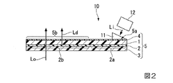
図2は、本発明の実施形態の画像表示用導光板を含む表示装置の一例を示す模式的な断面図である。
Next, an example of a display device including the image display
FIG. 2 is a schematic sectional view showing an example of a display device including the image display light guide plate according to the embodiment of the present invention.
図2に示すように、表示装置10は、画像表示用導光板5に加えて、画像光投影部12および入射光学系11を備える。
画像光投影部12は、図示略のコントローラから送出される画像信号に応じて、画像表示用導光板5に表示する画像光Liを投影する。
入射光学系11は、例えばプリズムなど、画像光Liを画像表示用導光板5に入射させる光学素子を備える。入射光学系11は、画像光Liを画像表示用導光板5の表面に形成された入射部5aに入射させる。例えば、入射部5aは、吸収層4上に設けられている。
入射部5aに入射した画像光Liは、ホログラム層2に形成された導波回折格子部3aを経由して、ホログラム層2の表示用回折格子部2bに導波される。表示用回折格子部2bでは、画像光Liは各表示画素に対応する位置で回折され、画像光Ldを形成する。画像光Ldは、ホログラム層2、樹脂基材1、および吸収層4を透過し、画像光Ld’として、画像表示用導光板5の外部に出射される。このため、厚み方向において表示用回折格子部2bと、表示用回折格子部2bと厚み方向に対向する樹脂基材1および吸収層4の領域は、画像光Ldを表示する表示画像出射部5bを構成している。表示画像出射部5bは、厚み方向と直交する方向である面方向において、入射部5aから離間した位置に形成されている。
As shown in FIG. 2, the
The image
The incident
The image light Li incident on the
一方、画像表示用導光板5には、樹脂基材3を経由して、外光Loが入射する。外光Loは、樹脂基材3、ホログラム層2、樹脂基材1、および吸収層4を透過し、外光Lo’として、画像表示用導光板5の外部に出射される。
表示装置10の使用者は、画像光Ld’および外光Lo’による像を見ることができる。このため、表示画像出射部5bを視野に収める使用者は、外光Lo’に基づく外部の光景と、画像光Ld’に基づく画像とが、重ね合わされた像を見る。
On the other hand, external light Lo is incident on the image display
The user of the
画像表示用導光板5に使用されるような透明材料は、例えば、紫外光などの影響によってそれぞれ経時的に光劣化する。典型的な光劣化は、材料の黄変である。特に、ホログラム層2は、フォトポリマー材料によって形成されているので、製造直後から、ある程度、黄変している。このため、樹脂基材1、3、およびホログラム層2を透過後の光は、黄色味を帯びている。
黄色は比視感度が高いので、人間の視覚は黄変に敏感である。これにより、黄色味を帯びた画像はコントラスト(明暗度)が低くなってしまうため、観察される画像が不鮮明になってしまう。
しかし、本実施形態では、表示画像出射部5bに吸収層4が設けられているので、画像光Ld’、外光Lo’において、それぞれ画像光Ld、外光Loの黄色成分が低減される。このように、吸収層4によって、黄色味を帯びた画像光Ld、外光Loの黄色成分が相殺されることにより、樹脂基材1、3、およびホログラム層2の黄変の影響が除去される。
具体的には、吸収層4によって、500nm以上600nm以下の波長範囲の光成分を中心に、光が吸収されることにより、黄色味が減少し、相対的に青色味が増大する。これにより、画像のホワイトバランスと、コントラストと、が改善される。
さらに、表示装置10の使用時に暴露される紫外光などによって、経時的に樹脂基材1、3等の透明材料の光劣化が進んでも、黄変による画像劣化の程度が吸収層4を有しない場合に比べて低減される。
The transparent material used for the image display
Since yellow has a high relative luminous sensitivity, human vision is sensitive to yellowing. As a result, the yellowish image has a low contrast (brightness), and the observed image becomes unclear.
However, in the present embodiment, since the
Specifically, the
Further, even if the photodegradation of the transparent material such as the
以上説明したように、本実施形態によれば、透明材料の黄変による表示画像への影響を低減できる画像表示用導光板を提供することができる。 As described above, according to this embodiment, it is possible to provide the image display light guide plate that can reduce the influence of the yellowing of the transparent material on the display image.
特に本実施形態では、吸収層4が画像表示用導光板5における最外部に配置されている。このため、例えば、吸収層4として、樹脂基材1よりも高硬度の材料を用いると、樹脂基材1の表面の傷つきが防止される。例えば、吸収層4の波長特性において紫外光の透過率が低い場合、樹脂基材1側からの紫外光の入射を抑制できるので、画像表示用導光板5における経時的な光劣化を低減できる。
Particularly in the present embodiment, the
[第1変形例]
本実施形態の第1変形例の画像表示用導光板について説明する。
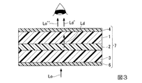
図3は、本発明の実施形態の第1変形例の画像表示用導光板の一例を示す模式的な断面図である。
[First Modification]
The image display light guide plate of the first modified example of the present embodiment will be described.
FIG. 3 is a schematic cross-sectional view showing an example of the image display light guide plate of the first modified example of the embodiment of the present invention.
図3に示すように、本変形例の画像表示用導光板7は、実施形態の画像表示用導光板5において、さらに吸収層6を備える。
以下、上記実施形態と異なる点を中心に説明する。
As shown in FIG. 3, the image display light guide plate 7 of the present modification example further includes an
The differences from the above embodiment will be mainly described below.
吸収層6は、樹脂基材3において、ホログラム層2が配置された表面と反対側の表面に積層されている。すなわち、吸収層6は、吸収層4と同様、画像表示用導光板7の最外部に配置されている。画像表示用導光板7では、樹脂基材1、ホログラム層2、および樹脂基材3からなる積層体が、吸収層4、6に挟まれている。
吸収層6としては、吸収層4の説明において例示されたのと同様の構成が用いられる。
ただし、吸収層6の厚み、材料等は、吸収層4と相違していてもよい。例えば、吸収層6は、画像表示用導光板7における表示画像出射側と反対側の表面に配置されるので、樹脂基材3あるいは吸収層4に比べて表面硬度が高い材料が用いられてもよい。
本変形例では、吸収層4、6が画像表示用導光板7の最外部に配置されるので、吸収層4、6の波長特性において紫外光の透過率が低いことがより好ましい。
The
As the
However, the thickness, material and the like of the
In this modification, since the
画像表示用導光板7は、樹脂基材3に吸収層6が形成される以外は、実施形態における画像表示用導光板5と同様にして製造される。吸収層6の形成方法は、吸収層4と同様の形成方法が用いられる。
The image display light guide plate 7 is manufactured in the same manner as the image display
本変形例による画像表示用導光板7は、吸収層6を有する以外は,画像表示用導光板5と同様に構成される。このため、画像光Ldは、画像表示用導光板5と同様にして、吸収層4を通過することによって黄色成分が低減される(画像光Ld’)。
これに対して、外光Loは、さらに吸収層6を透過してから、樹脂基材3に入射する。このため、外光Loは、吸収層6を透過する際に、黄色成分が低減される。外光Loは、樹脂基材3、ホログラム層2、および樹脂基材1を透過する際、それぞれの黄変度合いに応じて、黄色成分が増大した後、吸収層4によって黄色成分が低減される。
樹脂基材3は、使用時のおける外光Loの入射側に配置されているため、外光Loによる光劣化が進行しやすい。これにより、経時的には、樹脂基材1の黄変よりも樹脂基材3の黄変が進みやすいおそれがある。樹脂基材3の黄変が進むと、樹脂基材3を透過した外光Loは、樹脂基材3を透過しない画像光Ldに比べると黄色成分が強くなるおそれがある。
しかし、本変形例では、吸収層6を有するため、樹脂基材3の黄変による黄色味の増加を吸収層6によって相殺することが可能になる。このため、吸収層4から出射される外光Lo’’の黄色味が、画像表示用導光板5から出射される外光Lo’に比べて低減される。この結果、画像光Ld’と、外光Lo’’と、におけるそれぞれの黄色味のバランスを良好にすることができる。
特に、吸収層6の波長特性において紫外光の透過率が低い場合には、外光Loによる樹脂基材3の光劣化自体を低減できる。
The image display light guide plate 7 according to the present modification is configured similarly to the image display
On the other hand, the external light Lo is further transmitted through the
Since the
However, in this modified example, since the
In particular, when the transmittance of ultraviolet light is low in the wavelength characteristics of the
以上説明したように、本変形例によれば、透明材料の黄変による表示画像への影響を低減できる画像表示用導光板を提供することができる。 As described above, according to this modification, it is possible to provide the image display light guide plate that can reduce the influence of the yellowing of the transparent material on the display image.
[第2変形例]
本実施形態の第2変形例の画像表示用導光板について説明する。
図4は、本発明の実施形態の第2変形例の画像表示用導光板の一例を示す模式的な断面図である。
[Second Modification]
A light guide plate for image display of a second modified example of the present embodiment will be described.
FIG. 4 is a schematic cross-sectional view showing an example of the image display light guide plate of the second modified example of the embodiment of the present invention.
図4に示すように、本変形例の画像表示用導光板20は、第1変形例の画像表示用導光板7において、さらにバリア層8、9を備える。
以下、上記第1変形例と異なる点を中心に説明する。
As shown in FIG. 4, the image display
Hereinafter, the points different from the first modified example will be mainly described.
バリア層8は、樹脂基材1とホログラム層2との間に配置され、樹脂基材1およびホログラム層2のそれぞれの表面に密着している。バリア層8は、画像表示用導光板20の外部および樹脂基材1から浸透するガスがホログラム層2に浸透することを防止する。
バリア層8の材料としては、透明な無機材料が用いられる。バリア層8に用いる無機材料の種類は、ホログラム層2の劣化の要因となるガスをバリアできれば、特に限定されない。
バリア層8は、例えば、酸素透過率、水蒸気透過率が小さいほどより好ましい。特に、バリア層8は、水蒸気バリア性に優れる(水蒸気透過率が小さい)材料で構成されることがより好ましい。
例えば、バリア層8の酸素透過率は、1cm3/m2・day以下であってもよい。
例えば、バリア層8の水蒸気透過率は、1g/m2・day以下であってもよい。バリア層8の水蒸気透過率は、0.5g/m2・day以下であることがより好ましい。
The
A transparent inorganic material is used as the material of the
For example, the
For example, the oxygen permeability of the
For example, the water vapor transmission rate of the
バリア層8に用いる無機材料は、樹脂基材1よりも高い屈折率を有していてもよい。例えば、バリア層8の屈折率は、1.48以上3.0以下であってもよい。バリア層8が高屈折率であると、バリア層8を経由して樹脂基材1を透過する光は、光学的に密なバリア層8から光学的に粗な樹脂基材1に入射するため、バリア層8から樹脂基材1に向かう光の出射角が、バリア層8と樹脂基材1との屈折率差に応じて大きくなる。これにより、画像表示用導光板20におけるFOV(field of view)を広げることができる。
The inorganic material used for the
バリア層8の材料の例としては、例えば、珪素酸化物、珪素窒素酸化物、DLC、アルミニウム酸化物、などが挙げられる。例えば、バリア層8の材料は、酸化亜鉛、酸化アンチモン、酸化インジウム、酸化セリウム、酸化カルシウム、酸化カドミウム、酸化銀、酸化金、酸化クロム、酸化ケイ素、酸化コバルト、酸化ジルコニウム、酸化スズ、酸化チタン、酸化鉄、酸化銅、酸化ニッケル、酸化白金、酸化パラジウム、酸化ビスマス、酸化マ
グネシウム、酸化マンガン、酸化モリブデン、酸化バナジウムもしくは酸化バリウム等の酸化物であってもよい。
Examples of the material of the
バリア層8が珪素酸化物からなる場合、層厚としては、10nm以上300nm以下であってもよい。層厚が10nm未満であると、防湿性が不充分になるおそれがある。層厚が300nmを越えると珪素酸化物の薄膜に亀裂が起こりやすくなり、成膜面から剥離するおそれがある。
特に好ましい層厚としては、20nm以上200nm以下である。
珪素酸化物によってバリア層8を形成する方法は特に限定されない。例えば、バリア層8は、真空蒸着法、スパッタリング法、イオンプレーティング法、プラズマCVD法等の従来から知られているいずれかの方法で形成することができる。珪素酸化物によってバリア層8を形成する際、成膜面と珪素酸化物との接着性を向上させるために、成膜面にコロナ放電処理、低温プラズマ処理を施したり、また、シランカップリング剤、飽和ポリエステルとイソシアネートの混合物を塗布する等の表面処理を施したりしてもよい。
例えば、真空蒸着法によって珪素酸化物の薄膜を成膜する場合には、蒸発物質として珪素、一酸化珪素、二酸化珪素、またはこれらの混合物を用い、1.0×10⁻³Torr〜1.0×10⁻⁵Torrの真空下で、電子ビーム、抵抗加熱または高周波加熱方式で加熱蒸発させる。
また、酸素ガスを供給しながら行う反応蒸着法も採用できる。
バリア層8を形成する珪素酸化物には、10質量%以下であれば、その中に不純物としてカルシウム、マグネシウムまたはそれらの酸化物が混入していてもよい。
When the
A particularly preferable layer thickness is 20 nm or more and 200 nm or less.
The method of forming the
For example, when a silicon oxide thin film is formed by a vacuum evaporation method, silicon, silicon monoxide, silicon dioxide, or a mixture thereof is used as an evaporation substance, and 1.0×10 −3 Torr to 1.0 is used. It is heated and evaporated by electron beam, resistance heating, or high-frequency heating under a vacuum of ×10 -5 Torr.
Further, a reactive vapor deposition method performed while supplying oxygen gas can also be adopted.
If the silicon oxide forming the
バリア層8が珪素窒素酸化物からなる場合、珪素酸化物が珪素窒素酸化物に代えられた以外は、珪素酸化物を主成分とするバリア層8と同様の構成が用いられる。
When
DLCは、一般的にはダイヤモンド状の構造と、グラファイト状の構造と、水素原子を構造に含むポリエチレン様の高分子構造と、の三元系の構造からなる非晶質炭素材料である。DLCの生成に当たり、炭素源としてエチレン、アセチレン、ベンゼンなどの炭化水素を用いた場合には通常は水素を含む基本的に三元系の構造となる。
DLCは、硬質性、潤滑性、耐摩耗性、化学的安定性、耐熱性、表面平滑性などにすぐれている。DLCは、上述の緻密な高分子構造を形成するため、ガスバリア性、水蒸気バリア性にも優れる。
DLCによってバリア層8を形成する場合の形成方法は、特に限定されない。DLCコーティング方法は、例えば、プラズマCVD法、イオンプレーティング法、イオンビームスパッタリング法等の物理的蒸着法など、周知の適宜コーティング方法を用いることができる。
DLC is an amorphous carbon material having a ternary structure, which is generally a diamond-like structure, a graphite-like structure, and a polyethylene-like polymer structure containing hydrogen atoms in its structure. When a hydrocarbon such as ethylene, acetylene, or benzene is used as a carbon source for DLC formation, a basically ternary structure containing hydrogen is usually formed.
DLC is excellent in hardness, lubricity, wear resistance, chemical stability, heat resistance, surface smoothness and the like. Since DLC forms the dense polymer structure described above, it is also excellent in gas barrier properties and water vapor barrier properties.
The method of forming the
バリア層8がアルミニウム酸化物からなる場合、バリア層8は、例えば、Al2O3のみで形成されてもよいし、Al、AlO、Al2O3等が混じり合って形成されてもよい。アルミニウム酸化物層におけるAl:Oの原子数比は、アルミニウム酸化物層の作製条件によって異なる。バリア層8として使用できるアルミニウム酸化物層は、バリア性能が損なわれない範囲で微量(全成分に対して高々3%まで)の他成分が含まれてもよい。
アルミニウム酸化物層の層厚は、バリア性能の必要に応じて設定されればよい。例えば、アルミニウム酸化物層の層厚は、5nm以上800nm以下であってもよい。
アルミニウム酸化物によってバリア層8を形成する方法は特に限定されない。例えば、バリア層8は、真空蒸着法、スパッター法、イオンプレーティングなどのPVD法(物理蒸着法)、あるいは、CVD法(化学蒸着法)などが用いられてもよい。
例えば、真空蒸着法においては、蒸着源材料としてAl、Al2O3等が用いられ、蒸着源の加熱方式としては、抵抗加熱、高周波誘導加熱、電子ビ−ム加熱等が用いられてもよい。真空蒸着法においては、反応性ガスとして、酸素、窒素、水蒸気等を導入したり、オゾン添加、イオンアシスト等の手段を用いた反応性蒸着を用いたりしてもよい。さらに、成膜面に基板にバイアス等を加えたり、成膜面の温度を上昇、あるいは、冷却したりしてもよい。スパッター法やCVD法等のほかの成膜方法においても同様である。
When the
The layer thickness of the aluminum oxide layer may be set according to the need for barrier performance. For example, the layer thickness of the aluminum oxide layer may be 5 nm or more and 800 nm or less.
The method of forming the
For example, in the vacuum vapor deposition method, Al, Al 2 O 3 or the like may be used as a vapor deposition source material, and resistance heating, high frequency induction heating, electron beam heating or the like may be used as a heating method of the vapor deposition source. .. In the vacuum vapor deposition method, oxygen, nitrogen, water vapor or the like may be introduced as the reactive gas, or reactive vapor deposition using means such as ozone addition or ion assist may be used. Furthermore, a bias may be applied to the substrate on the film forming surface, the temperature of the film forming surface may be raised, or the substrate may be cooled. The same applies to other film forming methods such as the sputter method and the CVD method.
バリア層9は、バリア層8が形成されたホログラム層2の表面と反対側のホログラム層2の表面に積層されている。
バリア層9の構成は、バリア層8の説明において例示されたのと同様の構成が用いられる。ただし、バリア層9の材料、厚み等は、バリア層8と相違していてもよい。
The
As the configuration of the
このような画像表示用導光板20は、例えば、以下のようにして製造できる。
樹脂基材1、3が準備され、樹脂基材1、3の表面に、バリア層8、9がそれぞれ形成される。バリア層8、9の製造方法としては、バリア層8、9の材料に応じて適宜の製造方法が選択される。
例えば、バリア層8が形成された樹脂基材1におけるバリア層8の表面に、ホログラム形成用のフォトポリマー材料が塗布される。このとき、バリア層8の外周部には、ホログラム層2と同厚みの透明なシール層が設けられてもよい。この場合、フォトポリマー材料は、シール層で囲まれて形成された凹部に塗布される。シール層は、ホログラム層2の形成後にホログラム層2の外周部をシールする。
この後、フォトポリマー材料上に、バリア層9が形成された樹脂基材3が、バリア層9をフォトポリマー材料の方に向けられた状態で載置される。
ただし、上述の製造順序は一例である。例えば、バリア層9が形成された樹脂基材3にフォトポリマー材料が塗布されてから、バリア層8が形成された樹脂基材1がフォトポリマー材料上に載置されてもよい。
この後、減圧プレスによって、吸収層4、樹脂基材1、バリア層8、フォトポリマー材料、バリア層9、樹脂基材3、および吸収層6からなる積層体が貼り合わせられる。
この後、積層体のフォトポリマー材料に回折パターンに対応した干渉縞を形成し、フォトポリマー材料中に、回折格子を形成する。
このようにして、画像表示用導光板20が製造される。
Such an image display
For example, a hologram-forming photopolymer material is applied to the surface of the
Thereafter, the
However, the above manufacturing sequence is an example. For example, the
After that, a laminated body including the
Thereafter, interference fringes corresponding to the diffraction pattern are formed on the photopolymer material of the laminated body, and a diffraction grating is formed in the photopolymer material.
In this way, the image display
画像表示用導光板20は、バリア層8、9が追加された以外は、第1変形例の画像表示用導光板7と同様に構成される。
バリア層8、9は、DLCやケイ素酸化物など透明な無機材料からなるが、400nm〜480nmの波長範囲において、青色光を吸収しやすいために、青色成分の透過率が低下する結果、透過光が黄色味を帯びる。
このように、バリア層8は外光Loおよび画像光Ldの黄色味を、バリア層9は外光Loの黄色味を、それぞれ増大させやすい。しかし、本変形例では、第1変形例と同様、吸収層4、6を備えるので、吸収層4、6の波長特性を適宜調整することによって、バリア層8、9による黄色味の増加を相殺することができる。すなわち、吸収層4から出射される外光Lo’’’および画像光Ld’’の黄色味を低減することができる。さらに、第1変形例と同様にして、外光Lo’’’および画像光Ld’’の黄色味のバランスを良好にすることができる。
The image display
Although the barrier layers 8 and 9 are made of a transparent inorganic material such as DLC or silicon oxide, they easily absorb blue light in the wavelength range of 400 nm to 480 nm, and as a result, the transmittance of the blue component decreases, resulting in the transmitted light. Becomes yellowish.
As described above, the
以上説明したように、本変形例によれば、透明材料の黄変による表示画像への影響を低減できる画像表示用導光板を提供することができる。 As described above, according to this modification, it is possible to provide the image display light guide plate that can reduce the influence of the yellowing of the transparent material on the display image.
さらに画像表示用導光板20によれば、バリア層8、9を備えるため、ホログラム層2の経時劣化を抑制することができる。
Further, according to the image display
樹脂基材1、3のガスバリア性は、樹脂材料の種類によって程度の差はあるが、ガラスに比べると格段に低い。このため、樹脂基材1、3は、ガラスよりもより高い吸湿性および水蒸気透過性を有している。
この結果、画像表示用導光板5の外部のガスは、ある程度、樹脂基材1、3を透過したり、内部に蓄積したりする。特に樹脂基材1、3には、水分が蓄積しやすい。
しかし、外部から樹脂基材1、3に浸透したガスおよび水分は、画像表示用導光板20内で拡散してもバリア層8、9によって遮蔽される。これにより、ホログラム層2へのガスおよび水蒸気の浸透が抑制される。
例えば、ホログラム層2への水分の浸透が抑制されることにより、ホログラム層2の劣化が防止される。
さらに、画像表示用導光板20では、上述の層構成を有するため、ホログラム層2は、樹脂基材1、3と接触していない。これにより、画像表示用導光板20が高温環境下に配置されても、ホログラム層2が、樹脂基材1、3を浸食することが防止される。
Although the gas barrier properties of the
As a result, the gas outside the image display
However, the gas and water that have permeated the
For example, deterioration of the
Furthermore, since the image display
特に、バリア層8、9の屈折率が、樹脂基材1、3に比べて高屈折率であると、上述したように、バリア層8から樹脂基材1に向かう光の出射角が大きくなる。同様に、樹脂基材3からバリア層9に入射する光は、出射角が狭められる。このため、樹脂基材3側の外部から入射して、画像表示用導光板5を透過する光は、バリア層9を有しない場合に比べて、より広角の範囲の光が入射し、バリア層8を有しない場合に比べて、より広角の範囲に出射される。この結果、外部光の視野の範囲がより広がるとともに、表示側のFOVも広がる。
ホログラム層2からの画像光に関しては、上述したように、バリア層8から樹脂基材1に向かう光の出射角が大きくなる結果、バリア層8を有しない場合に比べて、表示画面のFOVが広がる。
特に、本実施形態では、バリア層8、9が、ホログラム層2上に積層されることによって、外部光および画像光の拡散位置と、表示画面を構成するホログラム層2の回折位置とが、近づくため、このため、ホログラム層2から離れた位置にバリア層8、9が設けられる場合に比べると、より鮮明な画像が広範囲の角度から観察可能になる。
In particular, if the refractive index of the barrier layers 8 and 9 is higher than that of the
As for the image light from the
Particularly, in the present embodiment, the barrier layers 8 and 9 are laminated on the
ここで、画像表示用導光板20における輝度値およびFOVの測定方法について、簡単に説明する。
画像表示用導光板20における輝度値は、画像表示用導光板5を画像表示用導光板20に代えた以外は上述の実施形態における表示装置10と同様の表示装置と、輝度計と、を用いて測定される。
輝度値の測定において、表示装置は、画像表示用導光板20の表示画像出射部の中心が輝度計の測定光軸上で輝度計と対向する位置に配置される。表示画像出射部と、輝度計と、の距離は、表示装置の装着時における使用者の目の位置に対応する距離である。例えば、表示装置がヘッドマウントディスプレイの場合、距離は15mmとされる。
輝度値は、表示装置に最大輝度の白色画像を表示させたときに輝度計で測定される輝度である。
Here, a method of measuring the brightness value and the FOV in the image display
For the brightness value in the image display
In the measurement of the brightness value, the display device is arranged at a position where the center of the display image emitting portion of the image display
The brightness value is the brightness measured by a brightness meter when a white image with the maximum brightness is displayed on the display device.
画像表示用導光板20のFOVの測定では、表示装置に最大輝度の白色画像を表示させた状態で、輝度計の測定光軸を表示画像出射部に対して傾斜させて輝度を測定する。例えば、輝度計はゴニオステージなどによって、画像表示用導光板20に対して垂直の位置から適宜角度傾斜する揺動可能に支持される。
FOVは、白色画像が見えなくなることに対応する輝度を閾値として、閾値以上の輝度が得られる角度範囲として求められる。閾値以上の輝度が−θ1から+θ2までの範囲で得られる場合、FOVは、θ1+θ2である。ここで、角度は、画像表示用導光板20の法線角度を0°とする。
In the measurement of the FOV of the
The FOV is obtained as an angular range in which the brightness corresponding to the disappearance of the white image is set as a threshold and the brightness equal to or higher than the threshold is obtained. When the brightness equal to or higher than the threshold value is obtained in the range of −θ1 to +θ2, the FOV is θ1+θ2. Here, regarding the angle, the normal angle of the image display
[第3変形例]
本実施形態の第3変形例の画像表示用導光板について説明する。
図5は、本発明の実施形態の第3変形例の画像表示用導光板の一例を示す模式的な断面図である。
[Third Modification]
An image display light guide plate of a third modification of the present embodiment will be described.
FIG. 5 is a schematic cross-sectional view showing an example of a light guide plate for image display of a third modified example of the embodiment of the present invention.
図5に示すように、本変形例の画像表示用導光板24は、実施形態の画像表示用導光板5の吸収層4が削除され、樹脂基材1、3に代えて、樹脂基材21、23(吸収層)を備える。
以下、上記実施形態と異なる点を中心に説明する。
As shown in FIG. 5, in the image display
The differences from the above embodiment will be mainly described below.
樹脂基材21は、樹脂基材1と同様のベース樹脂と、ベース樹脂に分散された色材と、を備える。
樹脂基材21が含有する色材は、実施形態における吸収層4と同様の色材が用いられる。色材の配合量は、樹脂基材21が実施形態における吸収層4と同様の光吸収性を有するように設定される。
樹脂基材23は、樹脂基材21と同様に構成される。
The
As the coloring material contained in the
The
画像表示用導光板24は、基材準備工程で準備される樹脂基材21、23が、それぞれのベース樹脂に色材が練り込まれた材料を用いて成形され、かつ吸収層形成工程が行われない以外は、実施形態における画像表示用導光板5と同様にして製造される。
In the image display
画像表示用導光板24は、吸収層が樹脂基材21、23によって形成される例になっている。
画像表示用導光板24によれば、樹脂基材21、23が吸収層になっているので、第1変形例と同様にして、外光および画像光における黄色味を低減できる。
The image display
According to the image display
以上説明したように、本変形例によれば、透明材料の黄変による表示画像への影響を低減できる画像表示用導光板を提供することができる。 As described above, according to this modification, it is possible to provide the image display light guide plate that can reduce the influence of the yellowing of the transparent material on the display image.
なお、上記実施形態および各変形例では、吸収層が画像表示用導光板の最外部に配置される場合の例で説明した。しかし、吸収層は、外光Loおよび画像光Ldの光路上であれば、どこに配置されても、画像表示用導光板から出射される光の黄色味を低減することができる。 In addition, in the said embodiment and each modified example, the case where the absorption layer was arrange|positioned at the outermost part of the image display light-guide plate was demonstrated. However, the absorption layer can reduce the yellow tint of the light emitted from the image display light guide plate, wherever it is arranged, on the optical paths of the external light Lo and the image light Ld.
上記実施形態および各変形例では、吸収層が、樹脂基材に接している場合の例で説明した。しかし、吸収層は、透明な樹脂フィルムに積層されていてもよい。この場合、例えば、樹脂フィルムに吸収層を形成してから、接着剤などを介して配置面に固定することができるので、吸収層の形成が容易になる。 In the above-mentioned embodiment and each modification, the example in which the absorption layer is in contact with the resin base material has been described. However, the absorption layer may be laminated on a transparent resin film. In this case, for example, since the absorbent layer can be formed on the resin film and then fixed to the arrangement surface via an adhesive or the like, the absorbent layer can be easily formed.
上記第2変形例では、ホログラム層の表裏面にバリア層が配置されている場合の例で説明した。しかし、樹脂基材を通して浸透する水分等を遮蔽する目的およびホログラム層と樹脂基材との接触を防止する目的では、バリア層は、樹脂基材とホログラム層との間に配置されていればよい。
ただし、この場合、バリア層とホログラム層との間に挟まれる透明層の吸湿性が高いと、透明層の側面を通して水分が浸透するおそれがある。このため、バリア層とホログラム層との間の透明層は、吸湿性が少ない材料で形成されることがより好ましい。バリア層とホログラム層との間の透明層が吸湿性を有している場合には、透明層の厚みが薄くすることがより好ましい。この場合、水分の浸透口となる側面の露出面積が低減されるので、吸湿される水分量を低減できる。
In the second modified example, an example in which the barrier layers are arranged on the front and back surfaces of the hologram layer has been described. However, the barrier layer may be disposed between the resin base material and the hologram layer for the purpose of blocking moisture or the like penetrating through the resin base material and for preventing the contact between the hologram layer and the resin base material. ..
However, in this case, if the hygroscopicity of the transparent layer sandwiched between the barrier layer and the hologram layer is high, water may penetrate through the side surface of the transparent layer. Therefore, it is more preferable that the transparent layer between the barrier layer and the hologram layer is made of a material having a low hygroscopic property. When the transparent layer between the barrier layer and the hologram layer has hygroscopicity, the thickness of the transparent layer is more preferably reduced. In this case, the exposed surface area of the side surface serving as a water permeation port is reduced, so that the amount of moisture absorbed can be reduced.
上記第2変形例では、バリア層が、ホログラム層および樹脂基材に接している場合の例で説明した。しかし、バリア層は、透明な樹脂フィルムに積層されていてもよい。この場合、例えば、樹脂フィルムにバリア層を形成してから、接着剤などを介して樹脂基材に固定することができるので、バリア層の形成が容易になる。 In the second modified example, the example in which the barrier layer is in contact with the hologram layer and the resin base material has been described. However, the barrier layer may be laminated on the transparent resin film. In this case, for example, since the barrier layer can be formed on the resin film and then fixed to the resin base material with an adhesive or the like, the barrier layer can be easily formed.
以下、実施形態の実施例1、2について、比較例1とともに説明する。本発明はこれら実施例により制限されるものではない。 Hereinafter, Examples 1 and 2 of the embodiment will be described together with Comparative Example 1. The present invention is not limited to these examples.
下記[表1]に各実施例、比較例に用いる樹脂基材および吸収層の構成、および評価結果について示す。 The following [Table 1] shows the configurations of the resin substrate and the absorption layer used in each of the examples and comparative examples, and the evaluation results.

[実施例1]
実施例1は、実施形態の画像表示用導光板5に対応する実施例である。
[表1]に示すように、樹脂基材1、3([表1]では「樹脂基材」)の材料としては、アクリル樹脂(PMMA)が用いられる。
樹脂基材1、3の形状は、いずれも60mm×60mm×1mmの矩形板である。
ホログラム層2は、各実施例および各比較例に共通である。ホログラム層2の材料としては、ビスフェノール系エポキシ樹脂jER(登録商標)1007(重合度n=10.8、エポキシ当量:1750−2200、三菱ケミカル製商品名)100重量部、トリエチレングリコールジアクリレート50重量部および4、4’−ビス(tert−ブチルフェニル)ヨードニウムヘキサフルオロフォスフェート5重量部、3,3’−カルボニルビス(7−ジエチルアミノ)クマリン0.5重量部を2- ブタノン100重量部に混合溶解してホログラム用の感光材料として用いられる。ホログラム層2の厚みは、5μmである。ホログラム層2の平面視の大きさは50mm×50mmである。
[Example 1]
Example 1 is an example corresponding to the image display
As shown in [Table 1], an acrylic resin (PMMA) is used as a material for the
The
The
次に、実施例1における画像表示用導光板5の製造工程について説明する。画像表示用導光板5は、以下に説明する基板準備工程、吸収層形成工程、および導光板作製工程をこの順に行うことによって製造される。
Next, a manufacturing process of the image display
[基板準備工程]
基板準備工程では、樹脂基材1、3の洗浄および乾燥が行われる。以下、樹脂基材1、3を区別する必要がない場合には、符号を省略し、単に樹脂基材と表記する。
樹脂基材は、中性洗浄剤であるセミクリーン(登録商標)M−LO(商品名;横浜油脂工業株式会社製)の5%界面活性剤水溶液に浸漬させた状態で5分間超音波洗浄される。
この後、樹脂基材は、超純水に浸漬させた状態で5分間超音波洗浄される。さらに、超純水による樹脂基材のすすぎが行われ、樹脂基材は風乾後に100℃のオーブンで窒素雰囲気下にて乾燥される。この後、風乾した評価サンプルBは、UVオゾン洗浄機にて1分間、UVオゾン洗浄される。
以上で、基板準備工程が終了する。
[Substrate preparation process]
In the substrate preparation step, the
The resin base material is ultrasonically cleaned for 5 minutes while being immersed in a 5% surfactant aqueous solution of Semi Clean (registered trademark) M-LO (trade name; manufactured by Yokohama Yushi Kogyo Co., Ltd.) which is a neutral cleaning agent. It
Then, the resin base material is ultrasonically cleaned for 5 minutes while being immersed in ultrapure water. Further, the resin base material is rinsed with ultrapure water, and the resin base material is air dried and then dried in an oven at 100° C. under a nitrogen atmosphere. Thereafter, the air-dried evaluation sample B is cleaned with UV ozone in a UV ozone cleaner for 1 minute.
This is the end of the substrate preparation process.
[吸収層形成工程]
吸収層形成工程では、樹脂基材1の表面に吸収層4([表1]では「吸収層」)を形成する。
100質量部のアクリレート(ユピマー(登録商標)UV−HH2100(商品名;三菱ケミカル株式会社製))に5質量部の光重合開始剤を加え、さらに色材として、ダイアレンジ(登録商標)ブルーを0.05質量部加えて、硬化性樹脂組成物(コート液)を調製する。
この硬化性樹脂組成物を、金属製バーコーターを用いて樹脂基材1上に塗布し、90℃で1分間乾燥後、紫外光照射装置を用いて500mJ/cm2の露光量で露光し、厚み5μmの吸収層を有する積層体を得る。
以上で、吸収層形成工程が終了する。
以下では、吸収層が形成された樹脂基材を中間積層体と称する。
[Absorption layer forming step]
In the absorption layer forming step, the absorption layer 4 (“absorption layer” in [Table 1]) is formed on the surface of the
To 100 parts by mass of acrylate (UPIMER (registered trademark) UV-HH2100 (trade name; manufactured by Mitsubishi Chemical Co., Ltd.)), 5 parts by mass of a photopolymerization initiator was added, and as a coloring material, Diarene (registered trademark) blue was added. A curable resin composition (coating liquid) is prepared by adding 0.05 part by mass.
This curable resin composition was applied onto the
This is the end of the absorbing layer forming step.
Below, the resin base material in which the absorption layer was formed is called an intermediate laminated body.
[導光板作製工程]
導光板作製工程では、中間積層体と、樹脂基材3と、を用いて画像表示用導光板5が製造される。
中間積層体の吸収層と反対側の表面の周縁部に、幅5mm、厚み5μmのシール層が塗布される。
シール層は、透明材料からなり、樹脂基材同士を互いに接着できる材料であれば、特に限定されないが、実施例1では、光接着剤ハードロック(登録商標)OP−1045K(商品名;電気化学工業株式会社製)が用いられる。
これにより、シール層で囲まれた開口部が50mm×50mmの大きさを有するシール層段差付き中間積層体が準備される。
この後、この中間積層体上に、ホログラム用フォトポリマー材料として上記感光材料がスピンコートによって塗布される。上記感光材料は、乾燥後厚みが5μmになるように塗布される。
この後、樹脂基材3を、シール層付きの中間積層体のバリア層と対向するように、シール層および上記感光材料上に積層し、減圧下にてプレス貼合する。プレス貼合の条件は、絶対圧5kPa、温度70℃、プレス圧0.04MPaである。
この後、プレス貼合された積層体の上記感光材料に回折格子を記録する。この工程では、積層体の温度が20℃に保たれる。回折格子は、積層体に、2つのレーザー光を照射し、それぞれの照射角度や強度を調整することで、必要な回折パターンが形成されるように干渉縞を形成する。これにより、上記感光材料に回折格子が記録される。
具体的な回折格子としては、入射部に入射した画像光として入射された赤色、緑色、青色の波長領域の各光を回折して、画像光の画素に対応する位置において、表示部から出射させるカラー表示用回折格子が形成される。
この後、積層体を20℃に保った状態で、紫外光(波長365、放射照度80W/cm2)が積層体の片面の方向から30秒間全面照射される。紫外光の光源としては、高圧水銀ランプが用いられる。
これにより、シール層が硬化し、実施例1の画像表示用導光板5が形成される。
[Light guide plate manufacturing process]
In the light guide plate manufacturing step, the image display
A seal layer having a width of 5 mm and a thickness of 5 μm is applied to the peripheral portion of the surface of the intermediate laminate opposite to the absorption layer.
The sealing layer is made of a transparent material and is not particularly limited as long as it is a material capable of adhering resin base materials to each other, but in Example 1, a photo-adhesive hard lock (registered trademark) OP-1045K (trade name; electrochemical) Industrial Co., Ltd.) is used.
As a result, an intermediate layered product with a seal layer step is prepared in which the opening surrounded by the seal layer has a size of 50 mm×50 mm.
Then, the photosensitive material as a hologram photopolymer material is applied onto the intermediate laminate by spin coating. The above light-sensitive material is applied so as to have a thickness of 5 μm after drying.
After that, the
After that, a diffraction grating is recorded on the above-mentioned light-sensitive material of the press-bonded laminate. In this step, the temperature of the laminated body is kept at 20°C. The diffraction grating forms interference fringes so that a necessary diffraction pattern is formed by irradiating the laminated body with two laser beams and adjusting the irradiation angles and intensities of the two laser beams. As a result, a diffraction grating is recorded on the photosensitive material.
As a specific diffraction grating, each light in the wavelength region of red, green, and blue that is incident as image light incident on the incident portion is diffracted and is emitted from the display portion at a position corresponding to a pixel of the image light. A diffraction grating for color display is formed.
Thereafter, with the laminated body kept at 20° C., ultraviolet light (wavelength 365, irradiance 80 W/cm 2 ) is entirely irradiated for 30 seconds from the direction of one side of the laminated body. A high pressure mercury lamp is used as a light source of ultraviolet light.
As a result, the seal layer is cured, and the image display
[実施例2]
実施例2は、第1変形例の画像表示用導光板7に対応する実施例である。
[表1]に示すように、実施例2は、吸収層が両面に設けられている。具体的には、吸収層6が樹脂基材3におけるホログラム層2と反対側の表面に形成されている。
本実施例では、吸収層6([表1]では「吸収層」)は、実施例1の吸収層4と同様に構成される。
このため、実施例2の基板準備工程は、実施例1と同様である。
実施例2の吸収層形性工程は、吸収層4を有する中間積層体の他に、吸収層6が形成された樹脂基材3からなる中間積層体を形成する点が、実施例1と異なる。
実施例2の導光板作製工程は、2枚の中間積層体が用いられる点が、実施例1と異なる。
[Example 2]
Example 2 is an example corresponding to the image display light guide plate 7 of the first modification.
As shown in [Table 1], in Example 2, the absorption layers were provided on both surfaces. Specifically, the
In this embodiment, the absorption layer 6 (“absorption layer” in [Table 1]) is configured in the same manner as the
Therefore, the substrate preparing process of the second embodiment is the same as that of the first embodiment.
The absorbent layer forming process of Example 2 is different from Example 1 in that, in addition to the intermediate laminate having the
The light guide plate manufacturing process of Example 2 is different from Example 1 in that two intermediate laminated bodies are used.
[比較例1]
[表1]および図5に示すように、比較例1の画像表示用導光板100は、樹脂基材1、ホログラム層2、および樹脂基材3がこの順に積層して構成される。すなわち、吸収層を有しない以外は、実施例1と同様に構成される。
比較例1の画像表示用導光板100は、吸収層形成工程が行われない以外は、実施例1と同様にして製造される。
[Comparative Example 1]
As shown in [Table 1] and FIG. 5, the image display
The image display
次に、各実施例、比較例の評価方法について説明する。評価としては、鮮明性評価が行われる。 Next, the evaluation method of each example and comparative example will be described. As the evaluation, sharpness evaluation is performed.
[鮮明性評価]
表示画像の鮮明性は、各画像表示用導光板を用いた各表示装置を用いて行われる。各表示装置は、各実施例、比較例の画像表示用導光板が用いられる以外は、表示装置10と同様に構成される。
評価に用いる画像としては、ホログラム層で回折された画像光による表示画像と、外光が透過する外光像と、が用いられる。
表示画像の入力画像としては、白色画像と、文字画像と、が用いられる。
外光像としては、表示装置から0.5m〜50m離れた室内、街、もしくは森林の景色が用いられる。外光像の評価においては、白色画像もしくは文字画像を、それぞれ表示して評価する。
評価は、白色画像および文字画像の見え方と、外光像の見え方を目視で判定することにより行われる。文字画像としては、大きさとして、視力に換算して0.1から2.0のサイズのひらがな、カタカナ、漢字、アラビア数字もしくはアルファベット等が表示される。
[Clearness evaluation]
The sharpness of the displayed image is achieved by using each display device using each image display light guide plate. Each display device is configured similarly to the
As the image used for evaluation, a display image by the image light diffracted by the hologram layer and an external light image through which external light is transmitted are used.
A white image and a character image are used as the input image of the display image.
As the outside light image, a landscape of a room, a town, or a forest 0.5 m to 50 m away from the display device is used. In the evaluation of the external light image, a white image or a character image is displayed and evaluated.
The evaluation is performed by visually determining the appearance of the white image and the character image and the appearance of the external light image. As the character image, hiragana, katakana, kanji, Arabic numerals or alphabets having a size of 0.1 to 2.0 converted into visual acuity are displayed as the size.
[表示画像の鮮明性評価の基準]
表示画像の鮮明性評価は、3段階で行われる。
白色画像において虹色が見えず、文字画像において、文字がはっきり見える場合、良い(good、[表1]では「○」と記載)と判定する。
白色画像においてわずかに虹色が見えるが、文字画像において、文字がはっきり見える場合、可(fair、[表1]では「△」と記載)と判定する。
白色画像において少なくとも一部に虹色が見え、かつ文字画像において、文字の輪郭がぼやけて見える場合、不可(no good、[表1]では「×」と記載)と判定する。
[Criteria for display image sharpness evaluation]
The sharpness evaluation of the display image is performed in three stages.
When the rainbow color is not visible in the white image and the character is clearly visible in the character image, it is determined to be good (good, described as “◯” in [Table 1]).
When the rainbow color is slightly visible in the white image but the character is clearly visible in the character image, it is determined to be acceptable (fair, described as “Δ” in [Table 1]).
When at least a part of the rainbow color appears in the white image and the outline of the character appears blurred in the character image, it is determined to be impossible (no good, described as “x” in [Table 1]).
[外光像の鮮明性評価の基準]
外光像の鮮明性評価は、4段階で行われる。
外光像における景色の色味が違和感なく、はっきり見える場合、とても良い(very good、[表1]では「◎」と記載)と判定する。
外光像における景色が若干暗く見える場合、良い(good、[表1]では「○」と記載)と判定する。
外光像における景色が暗く、色味に若干の違和感がある場合、可(fair、[表1]では「△」と記載)と判定する。
外光像による景色がぼやけて見える場合、不可(no good、[表1]では「×」と記載)と判定する。
[Criteria for evaluation of sharpness of outside light image]
The sharpness evaluation of the external light image is performed in four stages.
When the color tone of the scenery in the outside light image is clear and clearly visible, it is determined to be very good (very good, described as “⊚” in [Table 1]).
When the scene in the outside light image looks slightly dark, it is determined to be good (good, described as “◯” in [Table 1]).
When the scene in the outside light image is dark and the color is slightly uncomfortable, it is determined to be acceptable (fair, described as “Δ” in [Table 1]).
When the scenery by the outside light image looks blurry, it is determined to be impossible (no good, described as “x” in [Table 1]).
[耐候性試験]
鮮明性評価に用いる画像表示用導光板としては、耐候性試験を施すサンプル([表1]では「耐候性試験後」)と、耐候性試験を施さないサンプル([表1]では「耐候性試験前」)とが準備される。
耐候性試験は、紫外線フェードメーターU48AU(商品名;スガ試験機株式会社製)を用いて行われる。試験条件は、BP温度が63℃±3℃とされる。試験時間は、500時間とされる。
[Weather resistance test]
As the light guide plate for image display used for the sharpness evaluation, a sample subjected to a weather resistance test (“after weather resistance test” in [Table 1]) and a sample not subjected to a weather resistance test (“table resistance” in [Table 1]) "Before the test") is prepared.
The weather resistance test is performed using an ultraviolet fade meter U48AU (trade name; manufactured by Suga Test Instruments Co., Ltd.). The test condition is that the BP temperature is 63° C.±3° C. The test time is 500 hours.
[評価結果]
[表1]に示すように、実施例1の鮮明性は、表示画像および外光像のいずれも耐候性試験の前後を問わず、「良い」と評価される。実施例2の鮮明性は、外光像の耐候性試験間が「とても良い」である以外は、「良い」と評価される。
この評価結果から、実施例1、2では、吸収層を備えることにより、表示画像および外光像とも、鮮明性が良好であることが分かる。特に、実施例2では、外光の入射側にも吸収層が設けられているため、耐候性試験前の場合には、実施例1に比べて外光像の鮮明性が向上している。
これに対して、比較例1の鮮明性は、表示画像および外光像とも、耐候性試験前が「可」であり、実施例1、2よりも劣っている。耐候性試験後の場合に「不可」であり、実施例1、2よりも格段に劣っている。
[Evaluation results]
As shown in [Table 1], the sharpness of Example 1 is evaluated as “good” in both the displayed image and the external light image before and after the weather resistance test. The sharpness of Example 2 was evaluated as “good” except that the weather resistance test of the external light image was “very good”.
From this evaluation result, it is understood that in Examples 1 and 2, the display image and the external light image have good sharpness by including the absorption layer. In particular, in Example 2, since the absorption layer was provided also on the incident side of external light, the sharpness of the external light image was improved as compared with Example 1 before the weather resistance test.
On the other hand, the sharpness of Comparative Example 1 was “good” in both the display image and the external light image before the weather resistance test, which is inferior to that of Examples 1 and 2. It is “impossible” after the weather resistance test, and is significantly inferior to Examples 1 and 2.
以上、本発明の好ましい実施形態、各変形例、および実施例を説明したが、本発明はこれらの実施形態、各変形例、および実施例に限定されることはない。本発明の趣旨を逸脱しない範囲で、構成の付加、省略、置換、およびその他の変更が可能である。
また、本発明は前述した説明によって限定されることはなく、添付の特許請求の範囲によってのみ限定される。
Although the preferred embodiments, modifications and examples of the present invention have been described above, the present invention is not limited to these embodiments, modifications and examples. Additions, omissions, substitutions, and other changes can be made to the configuration without departing from the spirit of the present invention.
Also, the invention is not limited by the above description, but only by the appended claims.
本発明の画像表示用導光板は、樹脂基材を用いてもホログラム層の劣化を抑制でき、例えば、VR、ARアプリケーションの表示装置用途に有用である。例えば、本発明の画像表示用導光板は、ヘッドアップディスプレイ、ウェアラブルディスプレイ、ヘッドマウントディスプレイなど表示装置用途に有用である。 INDUSTRIAL APPLICABILITY The image display light guide plate of the present invention can suppress deterioration of the hologram layer even if a resin base material is used, and is useful, for example, for display device applications in VR and AR applications. For example, the light guide plate for image display of the present invention is useful for display device applications such as a head-up display, a wearable display and a head mounted display.
1、3 樹脂基材
2 ホログラム層
4、6 吸収層
5、7、20、24 画像表示用導光板
5b 表示画像出射部
8、9 バリア層
10 表示装置
21、23 樹脂基材(吸収層)
Li、Ld、Ld’、Ld’’ 画像光
Lo、Lo’、Lo’’、Lo’’’ 外光
1 and 3
Li, Ld, Ld', Ld'' image light Lo, Lo', Lo'', Lo''' outside light
Claims (6)
500nm以上600nm以下の波長範囲に吸収ピークを有する吸収層を含む
ことを特徴とする画像表示用導光板。 An image display light guide plate having a resin substrate and a hologram layer,
A light guide plate for image display, comprising an absorption layer having an absorption peak in a wavelength range of 500 nm to 600 nm.
請求項1に記載の画像表示用導光板。 The light guide plate for image display according to claim 1, wherein the absorption layer, the resin base material, and the hologram layer are arranged in this order in the thickness direction.
前記ホログラム層における表示画像出射部と厚み方向において重なる範囲に配置されている
請求項1に記載の画像表示用導光板。 The absorption layer is
The light guide plate for image display according to claim 1, wherein the light guide plate for image display is arranged in a range overlapping with a display image emitting portion in the hologram layer in a thickness direction.
前記樹脂基材の内部の少なくとも一部に色材が分散されて形成されている
請求項1に記載の画像表示用導光板。 The absorption layer is
The light guide plate for image display according to claim 1, wherein a coloring material is dispersed in at least a part of the inside of the resin base material.
請求項1に記載の画像表示用導光板。 The light guide plate for image display according to claim 1, further comprising a barrier layer.
請求項5に記載の画像表示用導光板。 The light guide plate for image display according to claim 5, wherein the barrier layer is arranged between the resin base material and the hologram layer.
Priority Applications (14)
| Application Number | Priority Date | Filing Date | Title |
|---|---|---|---|
| JP2019018945A JP2020126162A (en) | 2019-02-05 | 2019-02-05 | Light guide plate for image display |
| CN202411359721.1A CN118962989A (en) | 2019-02-05 | 2020-02-05 | Light guide plate for image display |
| TW109103501A TWI786368B (en) | 2019-02-05 | 2020-02-05 | Light guide plate for image display |
| CN202411359717.5A CN118962988A (en) | 2019-02-05 | 2020-02-05 | Light guide plate for image display |
| EP20753180.7A EP3923060A4 (en) | 2019-02-05 | 2020-02-05 | LIGHT GUIDE PLATE FOR IMAGE DISPLAY |
| KR1020217023048A KR102842856B1 (en) | 2019-02-05 | 2020-02-05 | Light guide plate for video display |
| CN202411359722.6A CN118962990A (en) | 2019-02-05 | 2020-02-05 | Light guide plate for image display |
| CN202080012156.5A CN113474714A (en) | 2019-02-05 | 2020-02-05 | Light guide plate for image display |
| KR1020247018668A KR20240095346A (en) | 2019-02-05 | 2020-02-05 | Light guide plate for image display |
| TW111101592A TWI808611B (en) | 2019-02-05 | 2020-02-05 | Light guide plate for image display |
| PCT/JP2020/004237 WO2020162476A1 (en) | 2019-02-05 | 2020-02-05 | Light guide plate for image display |
| US17/372,639 US12487560B2 (en) | 2019-02-05 | 2021-07-12 | Light guide plate for image display |
| US18/925,900 US20250044737A1 (en) | 2019-02-05 | 2024-10-24 | Light guide plate for image display |
| US19/375,651 US20260118820A1 (en) | 2019-02-05 | 2025-10-31 | Light guide plate for image display |
Applications Claiming Priority (1)
| Application Number | Priority Date | Filing Date | Title |
|---|---|---|---|
| JP2019018945A JP2020126162A (en) | 2019-02-05 | 2019-02-05 | Light guide plate for image display |
Publications (1)
| Publication Number | Publication Date |
|---|---|
| JP2020126162A true JP2020126162A (en) | 2020-08-20 |
Family
ID=72083977
Family Applications (1)
| Application Number | Title | Priority Date | Filing Date |
|---|---|---|---|
| JP2019018945A Pending JP2020126162A (en) | 2019-02-05 | 2019-02-05 | Light guide plate for image display |
Country Status (1)
| Country | Link |
|---|---|
| JP (1) | JP2020126162A (en) |
Cited By (3)
| Publication number | Priority date | Publication date | Assignee | Title |
|---|---|---|---|---|
| CN115903222A (en) * | 2021-08-05 | 2023-04-04 | 苏州苏大维格科技集团股份有限公司 | Augmented reality head-up display device, vehicle and preparation method of optical waveguide |
| JPWO2023058431A1 (en) * | 2021-10-06 | 2023-04-13 | ||
| CN117523153A (en) * | 2024-01-08 | 2024-02-06 | 中国核动力研究设计院 | A three-dimensional visualization method and device for reactor core data |
Citations (11)
| Publication number | Priority date | Publication date | Assignee | Title |
|---|---|---|---|---|
| JP2006162798A (en) * | 2004-12-03 | 2006-06-22 | Konica Minolta Photo Imaging Inc | Optical device, image display device, and head-mounted display |
| WO2007055390A1 (en) * | 2005-11-10 | 2007-05-18 | Teijin Chemicals Ltd. | Optical device and achromatic lens |
| JP2008139768A (en) * | 2006-12-05 | 2008-06-19 | Mitsubishi Chemicals Corp | Hologram optical recording medium |
| JP2010037380A (en) * | 2008-08-01 | 2010-02-18 | Teijin Chem Ltd | Aromatic polycarbonate resin composition for light guide plate and light guide plate |
| JP2013008657A (en) * | 2011-05-24 | 2013-01-10 | Sumitomo Chemical Co Ltd | Light guide plate |
| JP2015049278A (en) * | 2013-08-30 | 2015-03-16 | セイコーエプソン株式会社 | Optical device and image display unit |
| JP2015053163A (en) * | 2013-09-06 | 2015-03-19 | セイコーエプソン株式会社 | Optical device and image display apparatus |
| CN105487170A (en) * | 2016-01-19 | 2016-04-13 | 东南大学 | Holographic optical waveguide and holographic optical waveguide display device |
| JP2017050277A (en) * | 2015-09-01 | 2017-03-09 | Jsr株式会社 | Composition for light guide plate, light guide plate, and edge light type surface light-emitting device |
| WO2018135193A1 (en) * | 2017-01-20 | 2018-07-26 | ソニー株式会社 | Optical device and display device |
| JP2018123319A (en) * | 2017-02-01 | 2018-08-09 | 住友化学株式会社 | Polyimide film |
-
2019
- 2019-02-05 JP JP2019018945A patent/JP2020126162A/en active Pending
Patent Citations (11)
| Publication number | Priority date | Publication date | Assignee | Title |
|---|---|---|---|---|
| JP2006162798A (en) * | 2004-12-03 | 2006-06-22 | Konica Minolta Photo Imaging Inc | Optical device, image display device, and head-mounted display |
| WO2007055390A1 (en) * | 2005-11-10 | 2007-05-18 | Teijin Chemicals Ltd. | Optical device and achromatic lens |
| JP2008139768A (en) * | 2006-12-05 | 2008-06-19 | Mitsubishi Chemicals Corp | Hologram optical recording medium |
| JP2010037380A (en) * | 2008-08-01 | 2010-02-18 | Teijin Chem Ltd | Aromatic polycarbonate resin composition for light guide plate and light guide plate |
| JP2013008657A (en) * | 2011-05-24 | 2013-01-10 | Sumitomo Chemical Co Ltd | Light guide plate |
| JP2015049278A (en) * | 2013-08-30 | 2015-03-16 | セイコーエプソン株式会社 | Optical device and image display unit |
| JP2015053163A (en) * | 2013-09-06 | 2015-03-19 | セイコーエプソン株式会社 | Optical device and image display apparatus |
| JP2017050277A (en) * | 2015-09-01 | 2017-03-09 | Jsr株式会社 | Composition for light guide plate, light guide plate, and edge light type surface light-emitting device |
| CN105487170A (en) * | 2016-01-19 | 2016-04-13 | 东南大学 | Holographic optical waveguide and holographic optical waveguide display device |
| WO2018135193A1 (en) * | 2017-01-20 | 2018-07-26 | ソニー株式会社 | Optical device and display device |
| JP2018123319A (en) * | 2017-02-01 | 2018-08-09 | 住友化学株式会社 | Polyimide film |
Cited By (6)
| Publication number | Priority date | Publication date | Assignee | Title |
|---|---|---|---|---|
| CN115903222A (en) * | 2021-08-05 | 2023-04-04 | 苏州苏大维格科技集团股份有限公司 | Augmented reality head-up display device, vehicle and preparation method of optical waveguide |
| JPWO2023058431A1 (en) * | 2021-10-06 | 2023-04-13 | ||
| WO2023058431A1 (en) * | 2021-10-06 | 2023-04-13 | 株式会社Nttドコモ | Display device |
| JP7595185B2 (en) | 2021-10-06 | 2024-12-05 | 株式会社Nttドコモ | Display device |
| CN117523153A (en) * | 2024-01-08 | 2024-02-06 | 中国核动力研究设计院 | A three-dimensional visualization method and device for reactor core data |
| CN117523153B (en) * | 2024-01-08 | 2024-03-26 | 中国核动力研究设计院 | Three-dimensional visualization method and device for reactor core data |
Similar Documents
| Publication | Publication Date | Title |
|---|---|---|
| JP7758089B2 (en) | Light guide plate for image display and image display device | |
| US12487560B2 (en) | Light guide plate for image display | |
| JP6956909B2 (en) | Optical laminates and articles | |
| JP7326993B2 (en) | OPTICAL FILTER, MANUFACTURING METHOD THEREOF AND USE THEREOF | |
| JP4274147B2 (en) | Optical multilayer film and reflection type screen | |
| TW200912402A (en) | Polarizing plate | |
| JP2020126162A (en) | Light guide plate for image display | |
| JP7841226B2 (en) | Light guide plate for image display | |
| JP7042895B1 (en) | Optical laminates and articles | |
| JPH0495901A (en) | Method for manufacturing thin film optical elements | |
| JP3870449B2 (en) | Polarizing plate with antireflection layer | |
| JP2023132987A (en) | Light guide plate for image display | |
| JP7694050B2 (en) | Light guide plate for image display | |
| JP2022055331A (en) | Light guide plate for image display | |
| JP2022099540A (en) | Image display light guide plate | |
| JP2023132986A (en) | Light guide plate for image display | |
| KR101955753B1 (en) | Optical sheet and optical display apparatus comprising the same | |
| JP2023157234A (en) | Organic EL display device | |
| JP2022055621A (en) | Light guide plate for image display |
Legal Events
| Date | Code | Title | Description |
|---|---|---|---|
| A621 | Written request for application examination |
Free format text: JAPANESE INTERMEDIATE CODE: A621 Effective date: 20211222 |
|
| A131 | Notification of reasons for refusal |
Free format text: JAPANESE INTERMEDIATE CODE: A131 Effective date: 20221213 |
|
| A601 | Written request for extension of time |
Free format text: JAPANESE INTERMEDIATE CODE: A601 Effective date: 20230209 |
|
| A521 | Request for written amendment filed |
Free format text: JAPANESE INTERMEDIATE CODE: A523 Effective date: 20230411 |
|
| A131 | Notification of reasons for refusal |
Free format text: JAPANESE INTERMEDIATE CODE: A131 Effective date: 20230606 |
|
| A601 | Written request for extension of time |
Free format text: JAPANESE INTERMEDIATE CODE: A601 Effective date: 20230804 |
|
| A521 | Request for written amendment filed |
Free format text: JAPANESE INTERMEDIATE CODE: A523 Effective date: 20231003 |
|
| A131 | Notification of reasons for refusal |
Free format text: JAPANESE INTERMEDIATE CODE: A131 Effective date: 20231107 |
|
| A601 | Written request for extension of time |
Free format text: JAPANESE INTERMEDIATE CODE: A601 Effective date: 20240105 |
|
| A02 | Decision of refusal |
Free format text: JAPANESE INTERMEDIATE CODE: A02 Effective date: 20240423 |