JP2018536959A - Precharge of memory word line dependent channel - Google Patents
Precharge of memory word line dependent channel Download PDFInfo
- Publication number
- JP2018536959A JP2018536959A JP2018514399A JP2018514399A JP2018536959A JP 2018536959 A JP2018536959 A JP 2018536959A JP 2018514399 A JP2018514399 A JP 2018514399A JP 2018514399 A JP2018514399 A JP 2018514399A JP 2018536959 A JP2018536959 A JP 2018536959A
- Authority
- JP
- Japan
- Prior art keywords
- memory cell
- word line
- voltage
- nand string
- memory
- Prior art date
- Legal status (The legal status is an assumption and is not a legal conclusion. Google has not performed a legal analysis and makes no representation as to the accuracy of the status listed.)
- Granted
Links
Images


Classifications
-
- G—PHYSICS
- G11—INFORMATION STORAGE
- G11C—STATIC STORES
- G11C16/00—Erasable programmable read-only memories
- G11C16/02—Erasable programmable read-only memories electrically programmable
- G11C16/06—Auxiliary circuits, e.g. for writing into memory
- G11C16/10—Programming or data input circuits
-
- G—PHYSICS
- G11—INFORMATION STORAGE
- G11C—STATIC STORES
- G11C11/00—Digital stores characterised by the use of particular electric or magnetic storage elements; Storage elements therefor
- G11C11/56—Digital stores characterised by the use of particular electric or magnetic storage elements; Storage elements therefor using storage elements with more than two stable states represented by steps, e.g. of voltage, current, phase, frequency
- G11C11/5621—Digital stores characterised by the use of particular electric or magnetic storage elements; Storage elements therefor using storage elements with more than two stable states represented by steps, e.g. of voltage, current, phase, frequency using charge storage in a floating gate
- G11C11/5628—Programming or writing circuits; Data input circuits
-
- G—PHYSICS
- G11—INFORMATION STORAGE
- G11C—STATIC STORES
- G11C16/00—Erasable programmable read-only memories
- G11C16/02—Erasable programmable read-only memories electrically programmable
- G11C16/04—Erasable programmable read-only memories electrically programmable using variable threshold transistors, e.g. FAMOS
- G11C16/0483—Erasable programmable read-only memories electrically programmable using variable threshold transistors, e.g. FAMOS comprising cells having several storage transistors connected in series
-
- G—PHYSICS
- G11—INFORMATION STORAGE
- G11C—STATIC STORES
- G11C16/00—Erasable programmable read-only memories
- G11C16/02—Erasable programmable read-only memories electrically programmable
- G11C16/06—Auxiliary circuits, e.g. for writing into memory
- G11C16/08—Address circuits; Decoders; Word-line control circuits
-
- G—PHYSICS
- G11—INFORMATION STORAGE
- G11C—STATIC STORES
- G11C16/00—Erasable programmable read-only memories
- G11C16/02—Erasable programmable read-only memories electrically programmable
- G11C16/06—Auxiliary circuits, e.g. for writing into memory
- G11C16/24—Bit-line control circuits
-
- G—PHYSICS
- G11—INFORMATION STORAGE
- G11C—STATIC STORES
- G11C16/00—Erasable programmable read-only memories
- G11C16/02—Erasable programmable read-only memories electrically programmable
- G11C16/06—Auxiliary circuits, e.g. for writing into memory
- G11C16/34—Determination of programming status, e.g. threshold voltage, overprogramming or underprogramming, retention
- G11C16/3418—Disturbance prevention or evaluation; Refreshing of disturbed memory data
- G11C16/3427—Circuits or methods to prevent or reduce disturbance of the state of a memory cell when neighbouring cells are read or written
-
- G—PHYSICS
- G11—INFORMATION STORAGE
- G11C—STATIC STORES
- G11C16/00—Erasable programmable read-only memories
- G11C16/02—Erasable programmable read-only memories electrically programmable
- G11C16/06—Auxiliary circuits, e.g. for writing into memory
- G11C16/10—Programming or data input circuits
- G11C16/12—Programming voltage switching circuits
-
- G—PHYSICS
- G11—INFORMATION STORAGE
- G11C—STATIC STORES
- G11C2211/00—Indexing scheme relating to digital stores characterized by the use of particular electric or magnetic storage elements; Storage elements therefor
- G11C2211/56—Indexing scheme relating to G11C11/56 and sub-groups for features not covered by these groups
- G11C2211/562—Multilevel memory programming aspects
- G11C2211/5621—Multilevel programming verification
-
- H—ELECTRICITY
- H10—SEMICONDUCTOR DEVICES; ELECTRIC SOLID-STATE DEVICES NOT OTHERWISE PROVIDED FOR
- H10B—ELECTRONIC MEMORY DEVICES
- H10B41/00—Electrically erasable-and-programmable ROM [EEPROM] devices comprising floating gates
- H10B41/30—Electrically erasable-and-programmable ROM [EEPROM] devices comprising floating gates characterised by the memory core region
- H10B41/35—Electrically erasable-and-programmable ROM [EEPROM] devices comprising floating gates characterised by the memory core region with a cell select transistor, e.g. NAND
-
- H—ELECTRICITY
- H10—SEMICONDUCTOR DEVICES; ELECTRIC SOLID-STATE DEVICES NOT OTHERWISE PROVIDED FOR
- H10B—ELECTRONIC MEMORY DEVICES
- H10B43/00—EEPROM devices comprising charge-trapping gate insulators
- H10B43/20—EEPROM devices comprising charge-trapping gate insulators characterised by three-dimensional [3D] arrangements, e.g. with cells on different height levels
- H10B43/23—EEPROM devices comprising charge-trapping gate insulators characterised by three-dimensional [3D] arrangements, e.g. with cells on different height levels with source and drain on different levels, e.g. with sloping channels
- H10B43/27—EEPROM devices comprising charge-trapping gate insulators characterised by three-dimensional [3D] arrangements, e.g. with cells on different height levels with source and drain on different levels, e.g. with sloping channels the channels comprising vertical portions, e.g. U-shaped channels
Landscapes
- Engineering & Computer Science (AREA)
- Microelectronics & Electronic Packaging (AREA)
- Computer Hardware Design (AREA)
- Read Only Memory (AREA)
- Non-Volatile Memory (AREA)
- Semiconductor Memories (AREA)
Abstract
メモリデバイスをプログラミングするための技術が提供される。プリチャージ段階は、ビット線電圧が非選択NANDストリングのチャネルに達することを許容することによって、チャネルをブーストするために使用される。チャネルプリチャージを最大化し、またプログラムディスターブを最小化するために、ドレイン側ダミーワード線電圧は、選択ワード線の位置に基づいて制御される。ドレイン側ワード線電圧は、選択ワード線がドレイン側ダミーワード線に対して比較的遠い又は近い場合に、それぞれ比較的高い又は低くてもよい。ドレイン側ダミーワード線電圧が比較的高い場合、ビット線電圧は、チャネルを容易に通過しブーストすることができる。ドレイン側ダミーワード線電圧が比較的低い場合、ドレイン側データワード線のプログラムディスターブは、チャネル勾配が小さくなり、対応するホットキャリアの量が低減することによって、低減される。【選択図】図10Techniques for programming a memory device are provided. The precharge phase is used to boost the channel by allowing the bit line voltage to reach the channel of the unselected NAND string. In order to maximize channel precharge and minimize program disturb, the drain side dummy word line voltage is controlled based on the position of the selected word line. The drain side word line voltage may be relatively high or low, respectively, when the selected word line is relatively far or close to the drain side dummy word line. If the drain side dummy word line voltage is relatively high, the bit line voltage can easily pass through the channel and boost. When the drain side dummy word line voltage is relatively low, the program disturb of the drain side data word line is reduced by reducing the channel gradient and the corresponding amount of hot carriers. [Selection] Figure 10
Description
本技術は、メモリデバイスの動作に関する。 The present technology relates to the operation of a memory device.
半導体メモリデバイスは、さまざまな電子デバイスにおける使用のために一層普及してきている。例えば、不揮発性半導体メモリは、携帯電話、デジタルカメラ、携帯情報端末、モバイルコンピューティングデバイス、非モバイルコンピューティングデバイス、及び、他のデバイスにおいて使用される。 Semiconductor memory devices are becoming more popular for use in various electronic devices. For example, non-volatile semiconductor memory is used in mobile phones, digital cameras, personal digital assistants, mobile computing devices, non-mobile computing devices, and other devices.
フローティングゲート又は電荷捕捉材料などの電荷格納材料は、データ状態を表す電荷を格納するためにかかるメモリデバイスにおいて使用可能である。電荷捕捉材料は、3次元(3D)積層メモリ構造において垂直に、又は、2次元(2D)メモリ構造において水平に配置可能である。3Dメモリ構造の一例は、導電層と誘電体層とが交互に積層されたスタックを含むBit Cost Scalable(BiCS)アーキテクチャである。 Charge storage materials such as floating gates or charge trapping materials can be used in such memory devices to store charge representative of the data state. The charge trapping material can be arranged vertically in a three-dimensional (3D) stacked memory structure or horizontally in a two-dimensional (2D) memory structure. An example of a 3D memory structure is a Bit Cost Scalable (BiCS) architecture that includes a stack of alternating conductive and dielectric layers.
メモリデバイスは、例えば、ストリング内に配置可能であるメモリセルを含み、この場合、選択ゲートトランジスタは、ストリングのチャネルをソース線又はビット線に選択的に接続するためにストリングの端部に設けられる。しかしながら、かかるメモリデバイスを動作させる際にさまざまな課題が存在する。 The memory device includes, for example, a memory cell that can be placed in a string, where a select gate transistor is provided at the end of the string to selectively connect the channel of the string to a source line or bit line. . However, various problems exist when operating such a memory device.
プログラムディスターブを低減する方法でメモリデバイスをプログラミングする技術を提供する。対応するメモリデバイスも提供される。 Techniques for programming memory devices in a manner that reduces program disturb are provided. A corresponding memory device is also provided.
いくつかのメモリデバイスでは、メモリセルは、ブロック又はサブブロックでのNANDストリングなどで、互いにつなげられる。それぞれのNANDストリングは、ビット線に接続されるNANDストリングのドレイン側の1又は複数のドレイン側SGトランジスタ(SGDトランジスタ)と、ソース線に接続されるNANDストリングのソース側の1又は複数のソース側SGトランジスタ(SGSトランジスタ)と、の間で直列に接続される多数のメモリセルを含む。さらに、メモリセルは、制御ゲートを機能させる共通の制御線(例えばワード線)と配置され得る。ワード線のセットは、ブロックのソース側からブロックのドレイン側まで亘っている。 In some memory devices, memory cells are connected to each other, such as NAND strings in blocks or sub-blocks. Each NAND string includes one or more drain side SG transistors (SGD transistors) on the drain side of the NAND string connected to the bit line and one or more source sides on the source side of the NAND string connected to the source line. It includes a number of memory cells connected in series with an SG transistor (SGS transistor). Furthermore, the memory cells can be arranged with a common control line (for example, a word line) that allows the control gate to function. The set of word lines extends from the source side of the block to the drain side of the block.
プログラミング動作中、メモリセルはワード線プログラミング順序に従ってプログラミングされる。例えば、プログラミングは、ブロックのソース側のワード線で開始し、ブロックのドレイン側のワード線に進んでよい。1つの手法では、それぞれのワード線は、次のワード線をプログラミングする前に完全にプログラミングされる。例えば、第1のワード線WL0は、プログラミングが完了するまで1又は複数のプログラミングパスを使用してプログラミングされる。次に、第2のワード線WL1は、プログラミングが完了するまで1又は複数のプログラミングパスを使用してプログラミングされ、以下同様に続く。プログラミングパスは、図11に示されるように、各プログラムループ又は各プログラムベリファイ反復でワード線に印加される、増大するプログラム電圧のセットを含んでよい。ベリファイ動作は、メモリセルのプログラミングが完了しているか否かを判断するために、それぞれのプログラム電圧後に行われてよい。メモリセルに対するプログラミングは、完了する時、さらなるプログラミングからロックアウト可能であるが、後続のプログラムループにおいて他のメモリセルに対するプログラミングは継続する。 During the programming operation, the memory cells are programmed according to the word line programming order. For example, programming may begin with a word line on the source side of the block and proceed to a word line on the drain side of the block. In one approach, each word line is fully programmed before programming the next word line. For example, the first word line WL0 is programmed using one or more programming passes until programming is complete. The second word line WL1 is then programmed using one or more programming passes until programming is complete, and so on. The programming pass may include an increasing set of program voltages applied to the word line at each program loop or each program verify iteration, as shown in FIG. A verify operation may be performed after each program voltage to determine whether programming of the memory cell is complete. When programming to a memory cell is complete, it can be locked out from further programming, but programming to other memory cells continues in subsequent program loops.
従って、それぞれのプログラムループ中、選択NANDストリングは、プログラミングのために選択されるメモリセルを含み、非選択NANDストリングはプログラミングのために選択されるメモリセルを含まない。所与のNANDストリングは、プログラミング動作の開始時に選択可能であり、選択ワード線上の当該NANDストリングのメモリセルがプログラミングを完了すると、選択されなくなる。消去状態のままにする選択ワード線上のメモリセルに接続されるNANDストリングは、非選択NANDストリングとして残ることになる。 Thus, during each program loop, the selected NAND string includes memory cells that are selected for programming, and the unselected NAND string does not include memory cells that are selected for programming. A given NAND string can be selected at the beginning of a programming operation and is not selected once the memory cells of the NAND string on the selected word line have completed programming. NAND strings connected to memory cells on the selected word line that remain in the erased state will remain as unselected NAND strings.
各メモリセルは、プログラムコマンド内の書込みデータに従ってデータ状態に関連付けられてもよい。このデータ状態に基づいて、メモリセルは、消去状態を維持するか、又は消去状態とは異なるデータ状態(プログラムされたデータ状態)にプログラムされることになる。例えば、1セル当たり2ビットのメモリデバイスでは、消去状態と、A、B及びCデータ状態と称される3つのより高いデータ状態と、を含む4つのデータ状態が存在する(図12B参照)。1セル当たり3ビットのメモリデバイスでは、消去状態と、A、B、C、D、E、F及びGデータ状態と称される7つのより高いデータ状態と、を含む8つのデータ状態が存在する(図13を参照)。1セル当たり4ビットのメモリデバイスでは、消去状態と、A、B、C、D、E、F、G、H、I、J、K、L、M、N及びOデータ状態と称される15のより高いデータ状態と、を含む16のデータ状態が存在する。 Each memory cell may be associated with a data state according to write data in the program command. Based on this data state, the memory cell will remain in the erased state or will be programmed to a data state (programmed data state) different from the erased state. For example, in a 2-bit memory device per cell, there are four data states including an erased state and three higher data states referred to as A, B, and C data states (see FIG. 12B). In a memory device with 3 bits per cell, there are 8 data states including an erase state and 7 higher data states referred to as A, B, C, D, E, F and G data states. (See FIG. 13). In a memory device with 4 bits per cell, it is called the erase state and the A, B, C, D, E, F, G, H, I, J, K, L, M, N and O data states 15 There are 16 data states, including higher data states.
しかしながら、メモリセルは、プログラム電圧が印加されるときにプログラムディスターブに起因して誤ってプログラミングされる可能性がある。プログラムディスターブは、1つの手法では、選択ワード線から非選択ワード線内の各メモリセルまでの容量結合によって生じる可能性がある。例えば、非選択NANDストリングのメモリセルは、非選択NANDストリングと選択NANDストリングとによって共有されるワード線に印加される電圧によって妨害される可能性がある。書込みデータに基づいて消去状態を維持するメモリセルは、プログラムディスターブの影響を最も受けやすい。プログラムディスターブによって、これらメモリセルのVthは増大し、その結果、読出しエラーが生じる可能性がある。プログラムディスターブを低減するために、非選択NANDストリングのチャネルは、プログラム電圧が印加される前にブーストされる。ブーストは、例えば、0Vから8〜9Vまでの、非選択ワード線の電圧(Vpass)の増大によって主にもたらされる。この増大はチャネルに結合する。さらに、非選択NANDストリングの各端部における選択ゲートトランジスタは、容量結合によってチャネル電圧がより高くフローティングできるように、非導電状態で設けられる。 However, memory cells can be erroneously programmed due to program disturb when a program voltage is applied. Program disturb can occur in one approach due to capacitive coupling from the selected word line to each memory cell in the unselected word line. For example, the memory cells of an unselected NAND string can be disturbed by a voltage applied to a word line shared by the unselected NAND string and the selected NAND string. Memory cells that maintain an erased state based on write data are most susceptible to program disturb. Program disturb increases the Vth of these memory cells, which can result in read errors. In order to reduce program disturb, the channel of the unselected NAND string is boosted before the program voltage is applied. The boost is mainly brought about by an increase in the voltage (Vpass) of the unselected word line, for example from 0V to 8-9V. This increase is coupled to the channel. Further, the select gate transistors at each end of the non-selected NAND string are provided in a non-conductive state so that the channel voltage can be floated higher due to capacitive coupling.
Vpassが増大する前にさらにブーストさせるために、SGDトランジスタが導電状態にある間に、ビット線を介してチャネルをプリチャージしてもよい。1つの手法では、ダミーワード線が、データを格納するのに不適合なダミーメモリセルに接続される。1又は複数のダミーメモリセルは、チャネル勾配における段階的移行をもたらすためにNANDストリングのドレイン端に設けられてもよい。プリチャージがチャネルを通過することができるように、ダミーワード線を比較的高い電圧で設け、強力な導電状態でダミーメモリセルを設けてもよい。しかしながら、これによって、ダミーワード線とドレイン側データワード線との間のチャネル勾配が増大する可能性があり、それによって、電子正孔対が生成されて、ここで電子はブースト電位を低下させる可能性がある。 To further boost before Vpass increases, the channel may be precharged via the bit line while the SGD transistor is in a conductive state. In one approach, a dummy word line is connected to a dummy memory cell that is incompatible with storing data. One or more dummy memory cells may be provided at the drain end of the NAND string to provide a gradual transition in channel gradient. The dummy word line may be provided with a relatively high voltage and the dummy memory cell may be provided in a strong conductive state so that precharge can pass through the channel. However, this can increase the channel slope between the dummy word line and the drain side data word line, thereby creating electron-hole pairs, where electrons can lower the boost potential. There is sex.
さらに、選択ワード線が、非選択NANDストリングのドレイン側よりもソース側に比較的近い場合、選択ワード線とダミーワード線との間に多くのメモリセルがあることになり、これらのメモリセルはワード線プログラミング順序の結果として消去状態になる。これらのメモリセルの制御ゲートが0Vなどの低電圧である場合でも、これらのメモリセル下のチャネル領域は比較的高い導電状態にあることになるため、電子は、チャネル内移動し、チャネル内で消失する可能性がある。これは、消去状態のメモリセルのVthが、−1V未満など、0V未満であってもよいために成立する。メモリセルの制御ゲート電圧がメモリセルのVth及びドレイン電圧の合計を超える場合、メモリセルは導電状態にある。チャネルのこの導電部分は、比較的高い静電容量を有し、生成された電子を吸収できる。しかしながら、選択ワード線が、非選択NANDストリングのソース側よりもドレイン側に比較的近い場合、選択ワード線とダミーワード線との間のメモリセルはない又はわずかとなる。従って、電子を吸収するために利用可能であるチャネルの導電部分は比較的小さい。この結果、電子がブースト電位を低下させる可能性がより高くなる。 Furthermore, if the selected word line is relatively closer to the source side than the drain side of the unselected NAND string, there will be many memory cells between the selected word line and the dummy word line, and these memory cells As a result of the word line programming sequence, an erase state is entered. Even when the control gates of these memory cells are at a low voltage, such as 0V, the channel region under these memory cells will be in a relatively high conductive state, so that electrons move within the channel and within the channel. May disappear. This is true because Vth of an erased memory cell may be less than 0V, such as less than −1V. If the control gate voltage of the memory cell exceeds the sum of the Vth and drain voltages of the memory cell, the memory cell is in a conductive state. This conductive portion of the channel has a relatively high capacitance and can absorb the generated electrons. However, if the selected word line is relatively closer to the drain side than the source side of the unselected NAND string, there are no or few memory cells between the selected word line and the dummy word line. Thus, the conductive portion of the channel that can be used to absorb electrons is relatively small. As a result, there is a higher possibility that electrons will lower the boost potential.
実際に、電子は非選択NANDストリングのドレイン端においていくつかのメモリセルの距離分移動できる。本明細書に提供される技術は、上記の及び他の問題点に対処する。1つの態様では、チャネルのプリチャージを最大化し、またプログラムディスターブを最小化するために、ドレイン側ダミーワード線電圧は、選択ワード線の位置に基づいて制御される。ドレイン側ダミーワード線電圧は、選択ワード線が、ドレイン側ダミーワード線から比較的遠い又は近い場合、それぞれ比較的高い又は低い可能性がある。従って、ドレイン側ダミーワード線電圧は、ある調節範囲を有する。ドレイン側ダミーワード線電圧(Vwld1)が比較的高い場合、ビット線電圧はチャネルを容易に通過しブーストすることができる。ドレイン側ダミーワード線電圧が比較的低い場合、より小さいチャネル勾配及び対応するホットキャリアの量の低減に起因して、ドレイン側データワード線のプログラムディスターブは低減する。 In fact, electrons can move a distance of several memory cells at the drain end of the unselected NAND string. The techniques provided herein address these and other issues. In one aspect, the drain side dummy word line voltage is controlled based on the position of the selected word line in order to maximize channel precharge and minimize program disturb. The drain side dummy word line voltage may be relatively high or low, respectively, when the selected word line is relatively far or close to the drain side dummy word line. Therefore, the drain side dummy word line voltage has a certain adjustment range. When the drain side dummy word line voltage (Vwld1) is relatively high, the bit line voltage can easily pass through the channel and be boosted. When the drain side dummy word line voltage is relatively low, the program disturb of the drain side data word line is reduced due to the smaller channel slope and the corresponding reduction in the amount of hot carriers.
1つの手法では、Vwld1のより高い値は、選択ワード線が、例えば、データワード線の50〜75%又は50〜80%を含むワード線の第1のグループの中にあるときに使用され、Vwld1のより低電圧は、選択ワード線がデータワード線の残り(20〜50%)の中にあるときに使用される。1つの手法では、第1のドレイン側ダミーワード線の調節範囲よりも小さい調節範囲を有する第2のドレイン側ダミーワード線が使用される。 In one approach, a higher value of Vwld1 is used when the selected word line is in a first group of word lines that includes, for example, 50-75% or 50-80% of the data word lines, The lower voltage of Vwld1 is used when the selected word line is in the rest of the data word line (20-50%). In one approach, a second drain side dummy word line having an adjustment range smaller than the adjustment range of the first drain side dummy word line is used.
様々な他の特徴及び利点が後述される。 Various other features and advantages are described below.
図1は、例示的なメモリデバイスのブロック図である。メモリデバイス100は、1又は複数のメモリダイ108を含んでもよい。メモリダイ108は、メモリセルのアレイなどのメモリセルのメモリ構造126、制御回路110及び読出し/書込み回路128を含む。メモリ構造126は、行デコーダ124を介してワード線により、及び、列デコーダ132を介してビット線によりアドレス指定可能である。読出し/書込み回路128は、複数のセンスブロックSB1、SB2、…、SBp(センス回路)を含み、メモリセルのページが並列に読み出されるか又はプログラムされることを可能にする。典型的には、コントローラ122は、1又は複数のメモリダイ108と同じメモリデバイス100(例えば、着脱可能なストレージカード)に含まれる。コマンド及びデータは、データバス120を介してホスト140とコントローラ122との間で、及び、ライン118を介してコントローラと1又は複数のメモリダイ108との間で転送される。
FIG. 1 is a block diagram of an exemplary memory device.
メモリ構造は2D又は3Dであってもよい。メモリ構造は、3Dアレイを含む、メモリセルの1又は複数のアレイを含んでもよい。メモリ構造は、ウェハなどの単一の基板の(中にではなく)上に、介在する基板なしに複数のメモリレベルが形成されるモノリシック3次元メモリ構造を含んでもよい。メモリ構造は、シリコン基板上に配置された活性領域を有するメモリセルのアレイの1又は複数の物理レベルでモノリシックに形成される、任意の種類の不揮発性メモリを含んでもよい。メモリ構造は、関連する回路が基板の上にあるか又は内部にあるかに関わらず、メモリセルの動作に関連付けられた回路を有する不揮発性メモリデバイス内にあってもよい。 The memory structure may be 2D or 3D. The memory structure may include one or more arrays of memory cells, including a 3D array. The memory structure may include a monolithic three-dimensional memory structure in which multiple memory levels are formed on (but not in) a single substrate, such as a wafer, without an intervening substrate. The memory structure may include any type of non-volatile memory formed monolithically at one or more physical levels of an array of memory cells having active regions disposed on a silicon substrate. The memory structure may be in a non-volatile memory device having circuitry associated with the operation of the memory cell, regardless of whether the associated circuitry is on or within the substrate.
制御回路110は、読出し/書込み回路128と協働してメモリ構造126上でメモリ動作を実行し、ステートマシン112、オンチップアドレスデコーダ114、電力制御モジュール116を含む。ステートマシン112は、メモリ動作のチップレベル制御を提供する。記憶領域113は、例えば、図10のプロセスに関連して、例えば、さらに後述されるようにパラメータをプログラミングするために設けられてよい。
The
オンチップアドレスデコーダ114は、ホスト又はメモリコントローラによって使用されるアドレスと、デコーダ124及び132によって使用されるハードウェアアドレスとのアドレスインターフェースを提供する。電力制御モジュール116は、メモリ動作中にワード線及びビット線に供給される電力及び電圧を制御する。電力制御モジュール116は、ワード線、SGS及びSGDトランジスタ、ならびにソース線用のドライバを含んでもよい。センスブロックは、1つの手法では、ビット線ドライバを含んでもよい。SGSトランジスタはNANDストリングのソース端における選択ゲートトランジスタであり、SGDトランジスタはNANDストリングのドレイン端における選択ゲートトランジスタである。
On-
いくつかの実装形態では、構成要素のいくつかは組み合わせてもよい。様々な設計では、メモリ構造126を除く1又は複数の構成要素(単体又は組み合わせ)は、図10のフローチャートのステップを含む、本明細書に説明される技術を行うように構成される少なくとも1つの制御回路とみなしてもよい。例えば、制御回路は、制御回路110、ステートマシン112、デコーダ114/132、電力制御モジュール116、センスブロックSBb、SB2、…、SBp、読出し/書込み回路128、及びコントローラ122などのうちの任意の1つ又は組み合わせを含んでもよい。
In some implementations, some of the components may be combined. In various designs, one or more components (alone or in combination) except for the
オフチップコントローラ122は、プロセッサ122cと、ROM122a及びRAM122bなどの記憶デバイス(メモリ)と、エラー訂正コード(ECC)エンジン245と、を含んでもよい。ECCエンジンは、Vth分布の上端が高くなり過ぎるときに引き起こされる多数の読出しエラーを訂正することができる。
The off-
記憶デバイスは、命令の集合などのコードを含み、プロセッサは、本明細書に説明される機能を提供するために命令の集合を実行するように動作可能である。代替的には又は追加的に、プロセッサは、1又は複数のワード線内のメモリセルの予約領域など、メモリ構造の記憶デバイス126aからコードにアクセスしてもよい。
The storage device includes code, such as a set of instructions, and the processor is operable to execute the set of instructions to provide the functionality described herein. Alternatively or additionally, the processor may access code from a
例えば、コードは、プログラミング動作、読出し動作及び消去動作などのためのメモリ構造にアクセスするために、コントローラによって使用可能である。コードは、ブートコード及び制御コード(例えば、命令の集合)を含んでもよい。ブートコードは、ブート処理中又はスタートアップ処理中にコントローラを初期化し、コントローラがメモリ構造にアクセスできるようにするソフトウェアである。コードは、1又は複数のメモリ構造を制御するためにコントローラによって使用可能である。起動時、プロセッサ122cは、実行のためにROM122a又は記憶デバイス126aからブートコードを取り出し、ブートコードは、システムコンポーネントを初期化し、制御コードをRAM122bにロードする。制御コードは、RAMにロードされるとプロセッサによって実行される。制御コードは、メモリの制御及び割り当て、命令の処理の優先順位付け、及び、入力ポート及び出力ポートの制御などの基本タスクを実行するためのドライバを含む。
For example, code can be used by the controller to access memory structures for programming operations, read operations, erase operations, and the like. The code may include boot code and control code (eg, a set of instructions). Boot code is software that initializes the controller during the boot or start-up process and allows the controller to access the memory structure. The code can be used by a controller to control one or more memory structures. At startup,
一般的に、制御コードは、さらに後述されるフローチャートのステップを含む、本明細書に説明される機能を実行するための命令を含んでもよく、さらに後述されるものを含む電圧波形を提供してもよい。 In general, the control code may further include instructions for performing the functions described herein, including the steps of the flowcharts described below, and provide voltage waveforms including those described further below. Also good.
1つの実施形態では、ホストは、1又は複数のプロセッサと、本明細書に説明される方法を実行するように当該1又は複数のプロセッサをプログラミングするためのプロセッサ可読コード(例えば、ソフトウェア)を格納する1又は複数のプロセッサ可読記憶デバイス(RAM、ROM、フラッシュメモリ、ハードディスクドライブ、固体メモリ)と、を含む、コンピューティング機器(例えば、ラップトップ、デスクトップ、スマートフォン、タブレット、デジタルカメラ)である。ホストは、追加のシステムメモリ、1又は複数の入力/出力インターフェース、及び/又は、1又は複数のプロセッサと通信する1又は複数の入力/出力デバイスも含んでもよい。 In one embodiment, the host stores one or more processors and processor readable code (eg, software) for programming the one or more processors to perform the methods described herein. A computing device (eg, laptop, desktop, smartphone, tablet, digital camera) including one or more processor readable storage devices (RAM, ROM, flash memory, hard disk drive, solid state memory). The host may also include additional system memory, one or more input / output interfaces, and / or one or more input / output devices in communication with the one or more processors.
NANDフラッシュメモリに加えて他の種類の不揮発性メモリを使用してもよい。 In addition to the NAND flash memory, other types of nonvolatile memories may be used.
半導体メモリデバイスは、ダイナミックランダムアクセスメモリ(DRAM)デバイス又はスタティックランダムアクセスメモリ(SRAM)デバイスなどの揮発性メモリデバイス、抵抗変化型メモリ(ReRAM)、電気的消去可能ROM(EEPROM)、(EEPROMのサブセットとみなしてもよい)フラッシュメモリ、強誘電体ランダムアクセスメモリ(FRAM(登録商標))及び磁気抵抗ランダムアクセスメモリ(MRAM)などの不揮発性メモリデバイス、ならびに、情報を格納可能である他の半導体素子を含む。各種類のメモリデバイスは、異なる構成を有してもよい。例えば、フラッシュメモリデバイスは、NAND構成又はNOR構成で構成されてもよい。 Semiconductor memory devices include volatile memory devices such as dynamic random access memory (DRAM) or static random access memory (SRAM) devices, resistance change memory (ReRAM), electrically erasable ROM (EEPROM), (a subset of EEPROM) Non-volatile memory devices such as flash memory, ferroelectric random access memory (FRAM®) and magnetoresistive random access memory (MRAM), and other semiconductor elements capable of storing information including. Each type of memory device may have a different configuration. For example, the flash memory device may be configured in a NAND configuration or a NOR configuration.
メモリデバイスは、任意の組み合わせで、受動素子及び/又は能動素子から形成してもよい。非限定的な例として、受動半導体メモリ素子は、いくつかの実施形態では、アンチヒューズ又は相変化材料などの抵抗型スイッチング記憶素子、及び、任意でダイオード又はトランジスタなどのステアリング素子を含む、ReRAMデバイス素子を含む。さらに、非限定的な例として、能動半導体メモリ素子は、いくつかの実施形態では、フローティングゲート、導電性ナノ粒子、又は電荷格納誘電体材料などの電荷格納領域を有する素子を含む。 The memory devices may be formed from passive and / or active elements in any combination. As a non-limiting example, a passive semiconductor memory element, in some embodiments, includes a resistive switching storage element such as an antifuse or phase change material, and optionally a steering element such as a diode or transistor, a ReRAM device. Including elements. Further, by way of non-limiting example, active semiconductor memory devices include devices having charge storage regions, such as floating gates, conductive nanoparticles, or charge storage dielectric materials in some embodiments.
複数のメモリ素子は、直列に接続されるように、又は、各素子が個々にアクセス可能であるように構成されてもよい。非限定的な例として、NAND構成(NANDメモリ)におけるフラッシュメモリデバイスは、典型的には、直列に接続されるメモリ素子を有する。NANDストリングは、メモリセル及びSGトランジスタを含む直列接続トランジスタのセットの一例である。 The plurality of memory elements may be configured to be connected in series or to be individually accessible to each element. As a non-limiting example, flash memory devices in a NAND configuration (NAND memory) typically have memory elements connected in series. A NAND string is an example of a set of series connected transistors including memory cells and SG transistors.
NANDメモリアレイは、ストリングが、単一ビット線を共有し、グループとしてアクセスされる複数のメモリ素子から構成されるメモリの複数のストリングから、該アレイが構成されるように構成されてよい。代替的には、メモリ素子は、例えば、NORメモリアレイといった、各素子が個々にアクセス可能であるように構成されてもよい。NAND及びNORメモリ構成は例であり、メモリ素子は別の構成であってもよい。 A NAND memory array may be configured such that the array is composed of a plurality of strings of memory that are composed of a plurality of memory elements that are accessed as a group, the strings sharing a single bit line. Alternatively, the memory elements may be configured such that each element is individually accessible, eg, a NOR memory array. NAND and NOR memory configurations are examples, and the memory elements may have different configurations.
基板内に及び/又は基板に亘って位置する半導体メモリ素子は、2次元メモリ構造又は3次元メモリ構造など、2次元又は3次元で配置されてよい。 The semiconductor memory elements located within and / or across the substrate may be arranged in two or three dimensions, such as a two-dimensional memory structure or a three-dimensional memory structure.
2次元メモリ構造において、半導体メモリ素子は、単一平面又は単一メモリデバイスレベルに配置される。典型的には、2次元メモリ構造では、メモリ素子は、メモリ素子を支持する基板の主面に実質的に平行に延在する平面(例えば、x−y方向平面)に配置される。基板は、メモリ素子が形成される層に亘る又は層内のウェハであってよく、又は、基板は、メモリ素子の形成後にメモリ素子に取り付けられるキャリア基板であってよい。非限定的な例として、基板はシリコンなどの半導体を含んでもよい。 In a two-dimensional memory structure, the semiconductor memory elements are arranged on a single plane or a single memory device level. Typically, in a two-dimensional memory structure, the memory elements are arranged in a plane (eg, an xy plane) that extends substantially parallel to the major surface of the substrate that supports the memory elements. The substrate may be a wafer that spans or is within a layer in which the memory element is formed, or the substrate may be a carrier substrate that is attached to the memory element after formation of the memory element. As a non-limiting example, the substrate may include a semiconductor such as silicon.
メモリ素子は、複数の行及び/又は列などの、順序付けられたアレイにおいて単一メモリデバイスレベルで配置されてもよい。しかしながら、メモリ素子は、非正則構成又は非直交構成で配置されてもよい。メモリ素子はそれぞれ、ビット線及びワード線など、2つ以上の電極又は接触線を有してもよい。 Memory elements may be arranged at a single memory device level in an ordered array, such as multiple rows and / or columns. However, the memory elements may be arranged in a non-regular configuration or a non-orthogonal configuration. Each memory element may have more than one electrode or contact line, such as a bit line and a word line.
3次元メモリアレイは、メモリ素子が複数の平面又は複数のメモリデバイスレベルを占めることで、3次元の(すなわち、基板の主面に対して、z方向が実質的に鉛直であり、x及びy方向が実質的に平行である、x、y及びz方向の)構造を形成するように配置される。 A three-dimensional memory array has a three-dimensional (ie, the z-direction is substantially perpendicular to the major surface of the substrate, and x and y with the memory elements occupying multiple planes or multiple memory device levels. They are arranged to form a structure (in the x, y and z directions) whose directions are substantially parallel.
非限定的な例として、3次元メモリ構造は、複数の2次元メモリデバイスレベルのスタックとして垂直に配置されてよい。別の非限定的な例として、3次元メモリアレイは、複数の垂直な列(例えば、基板の主面に実質的に鉛直に、すなわち、y方向に延在する列)として配置されてもよく、それぞれのカラムは複数のメモリ素子を有する。列は、2次元構造で、例えば、x−y平面で配置されてよく、結果として、複数の垂直に積層されたメモリ面上の素子によるメモリ素子の3次元配置がもたらされる。3次元のメモリ素子の他の構成はまた、3次元メモリアレイを構成してもよい。 As a non-limiting example, the 3D memory structure may be arranged vertically as a stack of multiple 2D memory device levels. As another non-limiting example, a three-dimensional memory array may be arranged as a plurality of vertical columns (eg, columns extending substantially perpendicular to the major surface of the substrate, ie, in the y direction). Each column has a plurality of memory elements. The columns may be arranged in a two-dimensional structure, for example, in an xy plane, resulting in a three-dimensional arrangement of memory elements with elements on a plurality of vertically stacked memory surfaces. Other configurations of three-dimensional memory elements may also constitute a three-dimensional memory array.
非限定的な例として、3次元NANDメモリアレイでは、メモリ素子は、互いに結合されて、単一の水平方向の(例えば、x−y)メモリデバイスレベル内でNANDストリングを形成してもよい。代替的には、メモリ素子は、互いに結合されて、複数の水平方向のメモリデバイスレベルを横切る垂直NANDストリングを形成してもよい。他の3次元構造は、いくつかのNANDストリングが単一のメモリレベルでメモリ素子を有し、他のストリングが複数のメモリレベルに及ぶメモリ素子を有すると想定してもよい。3次元メモリアレイは、NOR構成及びReRAM構成で設計されてもよい。 As a non-limiting example, in a three-dimensional NAND memory array, memory elements may be coupled together to form a NAND string within a single horizontal (eg, xy) memory device level. Alternatively, the memory elements may be coupled together to form a vertical NAND string across multiple horizontal memory device levels. Other three-dimensional structures may assume that some NAND strings have memory elements at a single memory level and other strings have memory elements that span multiple memory levels. The three-dimensional memory array may be designed with a NOR configuration and a ReRAM configuration.
典型的には、モノリシック3次元メモリアレイにおいて、1又は複数のメモリデバイスレベルは、単一の基板の上に形成される。モノリシック3次元メモリアレイは、単一の基板内に少なくとも部分的に1又は複数のメモリ層を任意に有してもよい。非限定的な例として、基板はシリコンなどの半導体を含んでもよい。モノリシック3次元アレイでは、アレイの各メモリデバイスレベルを構成する層は、典型的には、アレイの下にあるメモリデバイスレベルの層上に形成される。しかしながら、モノリシック3次元メモリアレイの隣接メモリデバイスレベルの層は、メモリデバイスレベル間で共有されてよい、又はメモリデバイスレベル間に介在する層を有してよい。 Typically, in a monolithic three-dimensional memory array, one or more memory device levels are formed on a single substrate. A monolithic three-dimensional memory array may optionally have one or more memory layers at least partially within a single substrate. As a non-limiting example, the substrate may include a semiconductor such as silicon. In a monolithic three-dimensional array, the layers that make up each memory device level of the array are typically formed on the memory device level layers below the array. However, adjacent memory device level layers of a monolithic three-dimensional memory array may be shared between memory device levels, or may have layers intervening between memory device levels.
2次元アレイは、別個に形成してもよく、そして、複数層のメモリを有する非モノリシックメモリデバイスを形成するために共にパッケージングされてよい。例えば、非モノリシック積層メモリは、別個の基板上にメモリレベルを形成後、該メモリレベルが互いに重なり合うように積層することによって、構築されてもよい。基板は、積層前に薄くされてよい、又はメモリデバイスレベルから除去されてよいが、最初にメモリデバイスレベルが別個の基板上に形成されるため、結果として生じるメモリアレイはモノリシック3次元メモリアレイではない。さらに、複数の2次元メモリアレイ又は3次元メモリアレイ(モノリシック又は非モノリシック)は、別個のチップ上に形成後、積層チップメモリデバイスを形成するために共にパッケージングされてよい。 Two-dimensional arrays may be formed separately and may be packaged together to form a non-monolithic memory device having multiple layers of memory. For example, a non-monolithic stacked memory may be constructed by forming memory levels on separate substrates and then stacking such that the memory levels overlap each other. The substrate may be thinned prior to stacking or removed from the memory device level, but the memory device level is first formed on a separate substrate so that the resulting memory array is a monolithic 3D memory array. Absent. Further, a plurality of two-dimensional memory arrays or three-dimensional memory arrays (monolithic or non-monolithic) may be packaged together to form a stacked chip memory device after being formed on separate chips.
関連する回路は、典型的には、メモリ素子の動作に、かつメモリ素子との通信に必要とされる。非限定的な例として、メモリデバイスは、プログラミング及び読出しなどの機能を達成するためにメモリ素子を制御し駆動するために使用される回路を有してもよい。この関連する回路は、メモリ素子と同じ基板上及び/又は別個の基板上にあってよい。例えば、メモリ読出し/書込み動作用のコントローラは、別個のコントローラチップ上に及び/又はメモリ素子と同じ基板上に位置してもよい。 Associated circuitry is typically required for operation of the memory element and for communication with the memory element. As a non-limiting example, a memory device may have circuitry used to control and drive memory elements to accomplish functions such as programming and reading. This associated circuitry may be on the same substrate as the memory element and / or on a separate substrate. For example, the controller for memory read / write operations may be located on a separate controller chip and / or on the same substrate as the memory element.
この技術が、説明される2次元及び3次元の例示的な構造に限定されず、しかしながら、本明細書に説明されるように、かつ当業者に理解されるように、該技術の趣旨及び範囲内の全ての関係するメモリ構造を包含することを、当業者は認識するであろう。 This technique is not limited to the two-dimensional and three-dimensional exemplary structures described, however, as described herein and as will be understood by those skilled in the art, the spirit and scope of the technique Those skilled in the art will recognize that all relevant memory structures within are encompassed.
図2は、図1のメモリアレイ126の2次元構造の一例におけるメモリセルのブロックを示す。メモリアレイは多くのブロックを含んでもよい。それぞれの例のブロック200、210は、ブロックの間で共有される、多数のNANDストリング及び対応するビット線、例えば、BL0、BL1、…、を含む。各NANDストリングは、一端がドレイン選択ゲート(SGD)に接続され、ドレイン選択ゲートの制御ゲートは共通のSGD線を介して接続される。NANDストリングは、他端がソース選択ゲートに接続され、順に共通のソース線220に接続される。16本のワード線、例えば、WL0〜WL15は、ソース選択ゲートとドレイン選択ゲートとの間に延びている。場合によっては、ユーザデータを有さないダミーワード線はまた、選択ゲートトランジスタに隣接するメモリアレイにおいて使用されてもよい。かかるダミーワード線は、ある特定のエッジ効果からエッジデータワード線を遮蔽することができる。
FIG. 2 shows a block of memory cells in an example of a two-dimensional structure of the
メモリアレイにおいて設けてもよい1つの種類の不揮発性メモリは、フローティングゲートメモリである。図3A及び図3Bを参照されたい。他の種類の不揮発性メモリを使用してもよい。例えば、電荷捕捉メモリセルは、不揮発性を有するように電荷を格納するために導電性フローティングゲートの代わりに非導電性誘電体材料を使用する。図4A及び図4Bを参照されたい。酸化ケイ素、窒化ケイ素及び酸化ケイ素(「ONO」)で形成される3層誘電体は、導電性制御ゲートとメモリセルチャネルの上の半導電基板の表面との間に挟まれる。セルは、セルチャネルから窒化物に電子を注入することによってプログラミングされ、ここで、これらの電子は、限定される領域に捕捉され格納される。この格納された電荷は、その後、検出可能な方法で、セルのチャネルの一部分の閾値電圧を変更する。セルは、ホットホールを窒化物に注入することによって消去される。別個の選択トランジスタを形成するために、ドープしたポリシリコンゲートがメモリセルチャネルの一部分に亘って延在するスプリットゲート構成で、同様のセルを提供してもよい。 One type of non-volatile memory that may be provided in a memory array is a floating gate memory. See FIGS. 3A and 3B. Other types of non-volatile memory may be used. For example, charge trapping memory cells use a non-conductive dielectric material instead of a conductive floating gate to store charge so as to be non-volatile. Please refer to FIG. 4A and FIG. 4B. A three-layer dielectric formed of silicon oxide, silicon nitride and silicon oxide (“ONO”) is sandwiched between the conductive control gate and the surface of the semiconductive substrate above the memory cell channel. The cell is programmed by injecting electrons from the cell channel into the nitride, where these electrons are captured and stored in a limited area. This stored charge then alters the threshold voltage of a portion of the cell's channel in a detectable manner. The cell is erased by injecting hot holes into the nitride. Similar cells may be provided in a split gate configuration in which a doped polysilicon gate extends over a portion of the memory cell channel to form a separate select transistor.
別の手法では、NROMセルが使用される。2つのビットは、例えば、それぞれのNROMセルに格納され、ここで、ONO誘電体層は、ソース拡散及びドレイン拡散の間でチャネルに亘って延在する。1つのデータビットの電荷は、ドレインに隣接する誘電体層に局在化され、他のデータビットの電荷はソースに隣接する誘電体層に局在化される。多状態のデータ記憶は、誘電体内で空間的に分離された電荷格納領域のバイナリ状態を別個に読出すことによって得られる。他のタイプの不揮発性メモリも知られている。 Another approach uses NROM cells. Two bits are stored in each NROM cell, for example, where the ONO dielectric layer extends across the channel between the source and drain diffusions. The charge of one data bit is localized in the dielectric layer adjacent to the drain and the charge of the other data bit is localized in the dielectric layer adjacent to the source. Multi-state data storage is obtained by separately reading the binary states of the charge storage regions that are spatially separated within the dielectric. Other types of non-volatile memory are also known.
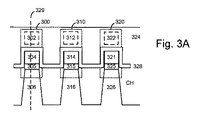
図3Aは、NANDストリングにおけるフローティングゲートメモリセルの一例の断面図を示す。ビット線又はNANDストリング方向はページの内部を向き、ワード線方向は左から右を向く。一例として、ワード線324は、各チャネル領域306、316及び326を含むNANDストリングに亘って延在する。メモリセル300は、制御ゲート302、フローティングゲート304、トンネル酸化層305及びチャネル領域306を含む。メモリセル310は、制御ゲート312、フローティングゲート314、トンネル酸化層315及びチャネル領域316を含む。メモリセル320は、制御ゲート322、フローティングゲート321、トンネル酸化層325及びチャネル領域326を含む。各メモリセルはそれぞれ、異なるNANDストリング内にある。ポリ間誘電体(IPD)層328も示される。制御ゲートはワード線の一部分である。線329に沿った断面図は図3Bに提供される。
FIG. 3A shows a cross-sectional view of an example of a floating gate memory cell in a NAND string. The bit line or NAND string direction points to the inside of the page, and the word line direction points from left to right. As an example,
制御ゲートは、フローティングゲートを取り囲み、制御ゲートとフローティングゲートとの間の表面接触面積を増大させる。これによって、IPD静電容量は高くなり、プログラミング及び消去をより容易くするように結合比が高くなる。しかしながら、NANDメモリデバイスは縮尺されるため、近隣セル間の間隔は小さくなり、そのため、制御ゲート及びIPDについて、2つの隣接フローティングゲート間の空間はほとんどない。代替として、図4A及び図4Bに示されるように、平坦な又は平面状のメモリセルは、制御ゲートが平坦又は平面状であるように開発されており、すなわち、制御ゲートはフローティングゲートを取り囲まず、電荷格納層とはただ、上から接触するだけである。この場合、高さのあるフローティングゲートを有することは利点にはならない。むしろ、フローティングゲートははるかに薄く作られる。さらに、フローティングゲートは、電荷を格納するために使用してもよい、又は、薄い電荷捕捉層は電荷を捕捉するために使用してもよい。この手法によって、電子が、プログラミング中にトンネル酸化物を突き抜けた後、フローティングゲートを移動することができるという、電子の弾道性伝導の問題を回避できる。 The control gate surrounds the floating gate and increases the surface contact area between the control gate and the floating gate. This increases the IPD capacitance and the coupling ratio to make programming and erasure easier. However, because NAND memory devices are scaled, the spacing between neighboring cells is small, so there is little space between two adjacent floating gates for the control gate and IPD. Alternatively, as shown in FIGS. 4A and 4B, flat or planar memory cells have been developed such that the control gate is flat or planar, ie, the control gate does not surround the floating gate. The charge storage layer simply contacts from above. In this case, having a floating gate with a height is not an advantage. Rather, the floating gate is made much thinner. Further, the floating gate may be used to store charge, or a thin charge trapping layer may be used to trap charge. This approach avoids the problem of ballistic conduction of electrons, where electrons can move through the floating gate after penetrating tunnel oxide during programming.
図3Bは、図3Aの構造の線329に沿った断面図を示す。NANDストリング330は、SGSトランジスタ331、例のメモリセル300、333、…、334及び335、ならびにSGDトランジスタ336を含む。メモリセルは、図3Aと合致するように、それぞれのメモリセルの例として、制御ゲート302、IPD層328、フローティングゲート304及びトンネル酸化層305を含む。SGS及びSGDトランジスタのIPD層における通路は、制御ゲート層及びフローティングゲート層を連通させることができる。例えば、制御ゲート層及びフローティングゲート層はポリシリコンであってよく、トンネル酸化層は酸化ケイ素であってよい。IPD層は、N−O−N−O−N構成などの窒化物(N)及び酸化物(O)のスタックとしてもよい。
FIG. 3B shows a cross-sectional view along
NANDストリングは、p型基板領域355、n型ウエル356及びp型ウエル357を含む基板上に形成されてもよい。N型ソース/ドレイン拡散領域sd1、sd2、sd3、sd4、sd5、sd6及びsd7はp型ウエルに形成される。チャネル電圧Vchは、基板のチャネル領域に直接印加されてよい。
The NAND string may be formed on a substrate including a p-
図4Aは、NANDストリングにおける例示的な電荷捕捉メモリセルの断面図を示す。この図は、図1のメモリセルアレイ126におけるメモリセルの2Dの例として、平坦な制御ゲート及び電荷捕捉領域を含むメモリセルのワード線方向の図である。電荷捕捉メモリは、NOR及びNANDフラッシュメモリデバイスにおいて使用してもよい。この技術は、電子を格納するために、ドープした多結晶ケイ素などの導電体を使用するフローティングゲートMOSFET技術と対照的に、電子を格納するためにSiN膜などの絶縁体を使用する。一例として、ワード線(WL)424は、各チャネル領域406、416及び426を含むNANDストリングに亘って延在する。ワード線の一部分は制御ゲート402、412及び422を提供する。ワード線より下には、IPD層428、電荷捕捉層404、414及び421、ポリシリコン層405、415及び425、ならびにトンネル層409、407及び408がある。それぞれの電荷捕捉層は、対応するNANDストリングにおいて途切れなく延在する。
FIG. 4A shows a cross-sectional view of an exemplary charge trapping memory cell in a NAND string. This figure is a diagram in the word line direction of a memory cell including a flat control gate and a charge trapping region as a 2D example of the memory cell in the
メモリセル400は、制御ゲート402、電荷捕捉層404、ポリシリコン層405及びチャネル領域406の一部分を含む。メモリセル410は、制御ゲート412、電荷捕捉層414、ポリシリコン層415及びチャネル領域416の一部分を含む。メモリセル420は、制御ゲート422、電荷捕捉層421、ポリシリコン層425及びチャネル領域426の一部分を含む。
ここで、平坦な制御ゲートは、フローティングゲートを取り囲む制御ゲートの代わりに使用される。1つの利点として、電荷捕捉層がフローティングゲートより薄く作られ得ることがある。さらに、メモリセルは互いに近くに設置可能である。 Here, a flat control gate is used instead of the control gate surrounding the floating gate. One advantage is that the charge trapping layer can be made thinner than the floating gate. Furthermore, the memory cells can be placed close to each other.
図4Bは、図4Aの構造の線429に沿った断面図を示す。この図は、平坦な制御ゲート及び電荷捕捉層を有するNANDストリング430を示す。NANDストリング430は、SGSトランジスタ431、例のメモリセル400、433、…、434及び435、ならびにSGDトランジスタ436を含む。
FIG. 4B shows a cross-sectional view along
NANDストリングは、p型基板領域455、n型ウエル456及びp型ウエル457を含む基板上に形成されてもよい。N型ソース/ドレイン拡散領域sd1、sd2、sd3、sd4、sd5、sd6及びsd7はp型ウエル457に形成される。チャネル電圧Vchは、基板のチャネル領域に直接印加されてよい。メモリセル400は、電荷捕捉層404より上の制御ゲート402及びIPD層428、ポリシリコン層405、トンネル層409、ならびにチャネル領域406を含む。
The NAND string may be formed on a substrate including a p-
例えば、制御ゲート層はポリシリコンであってよく、トンネル層は酸化ケイ素であってよい。IPD層は、制御ゲート層と電荷捕捉層又は電荷格納層との間の結合比の増大に寄与するAlOx又はHfOxなどの高k誘電体のスタックとしてもよい。電荷捕捉層は、例えば、窒化ケイ素及び酸化物の混合物としてもよい。 For example, the control gate layer may be polysilicon and the tunnel layer may be silicon oxide. The IPD layer may be a stack of a high-k dielectric such as AlOx or HfOx that contributes to an increased coupling ratio between the control gate layer and the charge trapping layer or charge storage layer. The charge trapping layer may be, for example, a mixture of silicon nitride and oxide.
SGD及びSGSトランジスタは、メモリセルと同じ構成を有するが、抑制されたNANDストリングで電流が遮断されることを確実にするためにより長いチャネル長を有している。 The SGD and SGS transistors have the same configuration as the memory cells, but have longer channel lengths to ensure that current is interrupted by the suppressed NAND string.
この例では、層404、405及び409は、NANDストリングにおいて途切れなく延在する。別の手法では、制御ゲート402、412及び422の間にある、層404、405及び409の一部分は、チャネル406の上面を露出するように、除去してもよい。
In this example, layers 404, 405, and 409 extend seamlessly in the NAND string. In another approach, portions of
図5は、図1のメモリアレイ126の例示的な3次元構造におけるブロックのセットを含むメモリデバイス600の斜視図である。基板上に、メモリセル(記憶素子)の例示的なブロックBLK0、BLK1、BLK2及びBLK3、ならびに、ブロックによる使用のための回路を有する周辺領域604がある。例えば、回路は、ブロックのゲート層を制御するために接続可能である電圧ドライバ605を含んでもよい。1つの手法では、ブロック内の共通の高さにおける制御ゲート層は、共通して駆動される。基板601は、回路の信号を伝送するために導通路においてパターン化される1又は複数の下部金属層に沿って、ブロックの下に回路を保持してもよい。ブロックは、メモリデバイスの中間領域602に形成される。メモリデバイスの上部領域603において、1又は複数の上部金属層が、回路の信号を伝送するために導通路においてパターン化される。各ブロックは、メモリセルの積層エリアを含み、ここで、スタックの交互のレベルはワード線を表す。1つの可能な手法では、各ブロックは、対向して層を成す側部を有しており、この側部から、導通路への接続を形成するために垂直接触部は上部金属層へと上方に延在する。一例として4つのブロックが示されるが、x方向及び/又はy方向に延在する2つ以上のブロックを使用することができる。
FIG. 5 is a perspective view of a
1つの可能な手法では、x方向における平面の長さは、ワード線への信号路が1又は複数の上部金属層に延在する方向(ワード線又はSGD線方向)を表し、y方向における平面の幅は、ビット線への信号路が1又は複数の上部金属層に延在する方向(ビット線方向)を表す。z方向はメモリデバイスの高さを表す。 In one possible approach, the length of the plane in the x direction represents the direction (word line or SGD line direction) in which the signal path to the word line extends to one or more upper metal layers, and the plane in the y direction. Represents the direction (bit line direction) in which the signal path to the bit line extends to one or more upper metal layers. The z direction represents the height of the memory device.
図6Aは、図5のブロックのうちの1つの一部分の例示的な断面図を示す。ブロックは、導電層と誘電体層とが交互に積層されたスタック610を含む。この例では、導電層は、データワード線層(ワード線)WLL0〜WLL10に加えて、2つのSGD層、2つのSGS層及び4つのダミーワード線層WLD1、WLD2、WLD3及びWLD4を含む。誘電体層にはDL0〜DL19の符号が付されている。さらに、NANDストリングNS1及びNS2を含むスタックの領域が示される。各NANDストリングは、ワード線に隣接するメモリセルを形成する材料が充填されるメモリホール618又は619を包含する。スタックの領域622は、図6Cにおいてより詳細に示される。
FIG. 6A shows an exemplary cross-sectional view of a portion of one of the blocks of FIG. The block includes a
スタックは、基板611、基板上の絶縁膜612及びソース線SLの一部分を含む。NS1は、スタックの最下部614においてソース端613を有し、スタックの最上部616においてドレイン端615を有する。金属充填スリット617及び620は、ソース線をスタックより上のラインに接続するなど、スタックを通して延在する相互接続としてスタックに亘って周期的に設けられてもよい。スリットは、ワード線の形成中に使用されてもよく、その後金属が充填されてもよい。ビット線BL0の一部分も示される。導電性ビア621はドレイン端615をBL0に接続する。
The stack includes a
図6Bは、図6Aのスタックにおけるメモリホール直径のプロットを示す。垂直軸は図6Aのスタックと整合し、メモリホール618及び619の幅(wMH)、例えば、直径を示す。かかるメモリデバイスでは、スタックからエッチングされるメモリホールは、アスペクト比が非常に高い。例えば、約25〜30の深さ対直径比が一般的である。メモリホールは円形の断面を有してもよい。エッチング処理によって、メモリホール幅は、ホールの長さに沿って変化し得る。典型的には、直径は、メモリホールの最上部から最下部に向かって次第に小さくなる(図6Bの実線)。すなわち、メモリホールは、スタックの最下部で狭くなるようにテーパ状になっている。場合によっては、メモリホールの最上部から最下部に向かって次第に小さくなる前に直径がわずかに広くなるように、選択ゲートの近くのホールの最上部においてわずかに狭くなる(図6Bの長い破線)。例えば、メモリホール幅は、この例では、スタック内のWLL9のレベルにおいて最大である。メモリホール幅は、WLL10のレベルにおいてわずかに小さくなり、WLL8〜WLL0のレベルで次第に小さくなる。
FIG. 6B shows a plot of memory hole diameter in the stack of FIG. 6A. The vertical axis is aligned with the stack of FIG. 6A and indicates the width (wMH), eg, diameter, of
短い破線で表される別の可能な実装形態では、2層のスタックが製造される。まず、対応するメモリホールと共に最下層が形成される。次いで、最下層におけるメモリホールと整合されるそれぞれのメモリホールと共に最上層が形成される。各メモリホールは、幅が増大した後に減少し、再び増大するようにスタックの最下部から最上部まで移動するダブルテーパのメモリホールが形成されるように、テーパ状になっている。 In another possible implementation represented by a short dashed line, a two-layer stack is produced. First, the lowermost layer is formed together with the corresponding memory hole. The top layer is then formed with each memory hole aligned with the memory hole in the bottom layer. Each memory hole is tapered such that a double taper memory hole is formed that moves from the bottom of the stack to the top so as to decrease and increase again after increasing in width.
メモリホールの幅の不均一性によって、メモリセルのプログラミング速度及び消去速度は、メモリホールに沿ったこれらの位置に基づいて、例えば、スタックにおけるこれらの高さに基づいて、変化し得る。メモリホールの直径が小さくなると、トンネル酸化物に亘る電界は、相対的により強力になるため、プログラミング速度及び消去速度は相対的に高くなる。 Due to the non-uniformity of the width of the memory holes, the programming speed and erasing speed of the memory cells can vary based on their position along the memory holes, for example based on their height in the stack. As the memory hole diameter decreases, the electric field across the tunnel oxide becomes relatively stronger so that the programming and erasing rates are relatively high.
ブロックは、3次元構造を含んでもよく、この構造において、メモリセルは垂直メモリホールに沿って配置され、垂直メモリホールは直径が変化し、それぞれのサブセットは同様の直径を有する垂直メモリホールの一部分に関連付けられる。 The block may include a three-dimensional structure in which the memory cells are arranged along vertical memory holes, the vertical memory holes vary in diameter, each subset being a portion of a vertical memory hole having a similar diameter. Associated with
図6Cは、図6Aのスタックの領域622の詳細図である。メモリセルは、ワード線層及びメモリホールの交点においてスタックの異なるレベルに形成される。この例では、SGDトランジスタ680及び681は、ダミーメモリセル682及び683、ならびにデータメモリセルMCより上に設けられる。多数の層は、例えば、原子層堆積を使用して、メモリホール630の側壁(SW)に沿って、及び/又は、各ワード線層内に堆積してもよい。例えば、それぞれの列(例えば、メモリホール内の材料によって形成されるピラー)は、SiN又は他の窒化物、トンネル層664、ポリシリコン体又はチャネル665、及び、誘電体コア666などの電荷捕捉層又は電荷捕捉膜663を含んでもよい。ワード線層は、ブロッキング酸化物/ブロック高k材料660、金属障壁661及び制御ゲートとしてのタングステンなどの導電性金属662を含んでもよい。例えば、制御ゲート690、691、692、693及び694が設けられる。この例では、金属以外の層の全てはメモリホールに設けられる。他の手法では、層のいくつかは制御ゲート層にあってもよい。追加のピラーは、異なるメモリホールに同様に形成される。ピラーは、NANDストリングの柱状活性領域(AA)を形成することができる。
FIG. 6C is a detailed view of
メモリセルがプログラミングされるとき、電子はメモリセルに関連付けられる電荷捕捉層の一部分に格納される。これらの電子は、チャネルからトンネル層を通って電荷捕捉層に引き込まれる。メモリセルのVthは、格納された電荷の量に比例して(例えば、増大に伴って)増大する。消去動作中、電子はチャネルに戻る。 When the memory cell is programmed, electrons are stored in a portion of the charge trapping layer associated with the memory cell. These electrons are drawn from the channel through the tunnel layer to the charge trapping layer. The Vth of the memory cell increases in proportion (eg, with increasing) to the amount of stored charge. During the erase operation, the electrons return to the channel.
メモリホールのそれぞれは、ブロッキング酸化層、電荷捕捉層、トンネル層及びチャネル層を含む複数の環状層が充填されてもよい。メモリホールのそれぞれのコア領域はボディ材料が充填され、複数の環状層はメモリホールのそれぞれにおいてコア領域とワード線との間にある。 Each of the memory holes may be filled with a plurality of annular layers including a blocking oxide layer, a charge trapping layer, a tunnel layer and a channel layer. Each core region of the memory hole is filled with a body material, and a plurality of annular layers are between the core region and the word line in each of the memory holes.
NANDストリングは、チャネルの長さが基板上で形成されないため、フローティングボディチャネルを有するとみなされてもよい。さらに、NANDストリングは、互いに積層させた複数のワード線層によって提供され、かつ、誘電体層によって互いに分離される。 NAND strings may be considered to have floating body channels because the channel length is not formed on the substrate. Further, the NAND string is provided by a plurality of word line layers stacked on each other and separated from each other by a dielectric layer.
図7Aは、図6Aのスタックの例示的なワード線層WLL10の上面図を示す。既述したように、3Dメモリデバイスは、導電層と誘電体層とが交互に積層されたスタックを含んでもよい。導電層は、SGトランジスタ及びメモリセルの制御ゲートを提供する。SGトランジスタに使用される層はSG層であり、メモリセルに使用される層はワード線層である。さらに、メモリホールは、スタックに形成され、電荷捕捉材料及びチャネル材料が充填される。この結果、垂直NANDストリングが形成される。ソース線はスタックの下でNANDストリングに接続され、ビット線はスタックの上でNANDストリングに接続される。 FIG. 7A shows a top view of an exemplary word line layer WLL10 of the stack of FIG. 6A. As described above, the 3D memory device may include a stack in which conductive layers and dielectric layers are alternately stacked. The conductive layer provides an SG transistor and a control gate for the memory cell. The layer used for the SG transistor is the SG layer, and the layer used for the memory cell is the word line layer. In addition, memory holes are formed in the stack and filled with charge trapping material and channel material. As a result, a vertical NAND string is formed. The source line is connected to the NAND string below the stack, and the bit line is connected to the NAND string above the stack.
3DメモリデバイスにおけるブロックBLKは、サブブロックに分割可能であり、この場合、各サブブロックは、共通のSGD制御線を有するNANDストリングのセットを含む。さらに、あるブロックにおけるワード線層は、複数領域に分割可能である。各領域は、メモリデバイスの製造プロセス中にワード線層を処理するためにスタックに周期的に形成されるスリット間に延在可能である。この処理は、ワード線層の犠牲材料を金属と置き換えることを含んでもよい。一般的に、スリット間の距離は、犠牲材料を除去するために腐食液が横方向に進行でき、金属が犠牲材料の除去によってもたらされる空隙を充填するために進行できる距離の限度を考慮して比較的小さいものとすべきである。例えば、スリット間の距離は、隣接スリット間のメモリホールの数行を許容してもよい。メモリホール及びスリットのレイアウトには、各ビット線が異なるメモリセルに接続される間に領域に亘って延在できるビット線の数の限度も考慮すべきである。ワード線層の処理後、スリットは、スタックを通じた相互接続をもたらすために金属により任意に充填してもよい。 A block BLK in a 3D memory device can be divided into sub-blocks, where each sub-block includes a set of NAND strings having a common SGD control line. Further, the word line layer in a certain block can be divided into a plurality of regions. Each region can extend between slits that are periodically formed in the stack to process the word line layer during the manufacturing process of the memory device. This process may include replacing the sacrificial material of the word line layer with metal. In general, the distance between the slits takes into account the limit of the distance that the etchant can travel laterally to remove the sacrificial material and the metal can travel to fill the voids created by the removal of the sacrificial material. Should be relatively small. For example, the distance between slits may allow several rows of memory holes between adjacent slits. The layout of the memory holes and slits should also take into account the limit on the number of bit lines that can extend across the region while each bit line is connected to a different memory cell. After processing the word line layer, the slits may optionally be filled with metal to provide interconnection through the stack.
この図及び他の図は、必ずしも縮尺通りではない。実際は、領域は、追加のメモリホールを収容するために、示されるよりも、y方向に対してx方向においてはるかに長くなっていてもよい。 This and other figures are not necessarily to scale. In practice, the region may be much longer in the x direction relative to the y direction than shown to accommodate additional memory holes.
この例では、隣接スリット間にメモリホールの4つの行がある。ここでの行は、x方向に整合されるメモリホールのグループである。さらに、メモリホールの行は、メモリホールの密度を高めるためにジグザグ状になっている。ワード線層は、それぞれがコネクタ713によって接続される領域WLL10a、WLL10b、WLL10c及びWLL10dに分割される。あるブロックにおけるワード線層の最終領域は、1つの手法では、次のブロックにおけるワード線層の第1の領域に接続可能である。そして、コネクタは、ワード線層用の電圧ドライバに接続される。領域WLL10aは、線712に沿った、例示的なメモリホール710及び711を有する。図7B及び図8を参照されたい。領域WLL10bは例示的なメモリホール714及び715を有する。領域WLL10cは例示的なメモリホール716及び717を有する。領域WLL10dは例示的なメモリホール718及び719を有する。各メモリホールは対応するNANDストリングの一部としてもよい。例えば、メモリホール710、714、716及び718は、それぞれNANDストリングNS0_SBa、NS0_SBb、NS0_SBc及びNS0_SBdの一部としてもよい。
In this example, there are four rows of memory holes between adjacent slits. The row here is a group of memory holes aligned in the x direction. Furthermore, the rows of memory holes are zigzag shaped to increase the density of memory holes. The word line layer is divided into regions WLL10a, WLL10b, WLL10c, and WLL10d each connected by a
各円は、ワード線層又はSG層におけるメモリホールの断面を表す。各円は、代替的には、メモリホールの材料によって及び隣接するワード線層によってもたらされるメモリセルを表すことができる。 Each circle represents a cross section of the memory hole in the word line layer or the SG layer. Each circle can alternatively represent a memory cell brought about by the material of the memory hole and by the adjacent word line layer.
金属充填スリット701、702、703及び704(例えば、金属相互接続)は、領域WLL10a〜WLL10dの縁部間に、これらに隣接して位置してもよい。金属充填スリットは、スタックの最下部からスタックの最上部までの導通路を提供する。例えば、スタックの最下部のソース線は、スタックの上の導電線に接続してもよく、ここで、導電線はメモリデバイスの周辺領域において電圧ドライバに接続される。図7AのサブブロッSBa〜SBdのさらなる詳細については、図8も参照されたい。
Metal filled
図7Bは、図6Aのスタックの例示的な最上部の誘電体層DL19の上面図を示す。誘電体層は領域DL19a、DL19b、DL19c及びDL19dに分割される。各領域はそれぞれの電圧ドライバに接続してもよい。これによって、ワード線層の1つの領域におけるメモリセルのセットを同時にプログラミングすることができ、各メモリセルは、それぞれのビット線に接続されるそれぞれのNANDストリングにある。電圧は、各プログラム電圧の間のプログラミングを可能にする又は阻止するために各ビット線上で設定してもよい。 FIG. 7B shows a top view of an exemplary top dielectric layer DL19 of the stack of FIG. 6A. The dielectric layer is divided into regions DL19a, DL19b, DL19c and DL19d. Each region may be connected to a respective voltage driver. This allows a set of memory cells in one region of the word line layer to be programmed simultaneously, each memory cell being in a respective NAND string connected to a respective bit line. The voltage may be set on each bit line to allow or prevent programming during each program voltage.
領域DL19aは、ビット線BL0と一致する線712aに沿って例示的なメモリホール710及び711を有する。多数のビット線は、メモリホールの上で延在し、符号「X」で示されるようにメモリホールに接続される。BL0はメモリホール711、715、717及び719を含むメモリホールのセットに接続される。別の例示的なビット線BL1は、メモリホール710、714、716及び718を含むメモリホールのセットに接続される。図7Aによる金属充填スリット701、701、703及び704も、スタックを通じて垂直に延在するように示される。ビット線は、−x方向においてDL19層に亘ってシーケンスBL0〜BL23で番号付けしてもよい。
Region DL19a has
ビット線の異なるサブセットは異なる行におけるセルに接続される。例えば、BL0、BL4、BL8、BL12、BL16及びBL20は、各領域の右方向縁部においてセルの第1の行におけるセルに接続される。BL2、BL6、BL10、BL14、BL18及びBL22は、右方向縁部において第1の行に隣接する、セルの隣接行におけるセルに接続される。BL3、BL7、BL11、BL15、BL19及びBL23は、各領域の左方向縁部においてセルの第1の行におけるセルに接続される。BL1、BL5、BL9、BL13、BL17及びBL21は、左方向縁部において第1の行に隣接する、セルの隣接行におけるセルに接続される。 Different subsets of bit lines are connected to cells in different rows. For example, BL0, BL4, BL8, BL12, BL16 and BL20 are connected to the cells in the first row of cells at the right edge of each region. BL2, BL6, BL10, BL14, BL18, and BL22 are connected to cells in adjacent rows of cells that are adjacent to the first row at the right edge. BL3, BL7, BL11, BL15, BL19 and BL23 are connected to the cells in the first row of cells at the left edge of each region. BL1, BL5, BL9, BL13, BL17, and BL21 are connected to cells in adjacent rows of cells that are adjacent to the first row at the left edge.
図8は、図7AのサブブロックSBa〜SBdにおける例示的なNANDストリングを示す。サブブロックは図6Aの構造と合致している。スタックにおける導電層は、左側における参照で示される。各サブブロックは複数のNANDストリングを含み、ここでNANDストリングの一例が示される。例えば、SBaは例示的なNANDストリングNS0_SBaを含み、SBbは例示的なNANDストリングNS0_SBbを含み、SBcは例示的なNANDストリングNS0_SBcを含み、SBdは例示的なNANDストリングNS0_SBdを含む。 FIG. 8 shows an exemplary NAND string in sub-blocks SBa-SBd of FIG. 7A. The sub-block is consistent with the structure of FIG. 6A. The conductive layer in the stack is indicated by reference on the left side. Each sub-block includes a plurality of NAND strings, where an example of a NAND string is shown. For example, SBa includes an exemplary NAND string NS0_SBb, SBb includes an exemplary NAND string NS0_SBb, SBc includes an exemplary NAND string NS0_SBc, and SBd includes an exemplary NAND string NS0_SBd.
さらに、NS0_SBaは、SGSトランジスタ800及び801、ダミーメモリセル802及び803、データメモリセル804、805、806、807、808、809、810、811、812、813及び814、ダミーメモリセル815及び816、ならびにSGDトランジスタ817及び818を含む。
Further, NS0_SBa includes
NS0_SBbは、SGSトランジスタ820及び821、ダミーメモリセル822及び823、データメモリセル824、825、826、827、828、829、830、831、832、833及び834、ダミーメモリセル835及び836、ならびにSGDトランジスタ837及び838を含む。
NS0_SBb includes
NS0_SBcは、SGSトランジスタ840及び841、ダミーメモリセル842及び843、データメモリセル844、845、846、847、848、849、850、851、852、853及び854、ダミーメモリセル855及び856、ならびにSGDトランジスタ857及び858を含む。
NS0_SBc includes
NS0_SBdは、SGSトランジスタ860及び861、ダミーメモリセル862及び863、データメモリセル864、865、866、867、868、869、870、871、872、873及び874、ダミーメモリセル875及び876、ならびにSGDトランジスタ877及び878を含む。
NS0_SBd includes
WLL8におけるメモリセルは、メモリセル812、832、852及び872を含む。WL9におけるメモリセルは、メモリセル813、833、853及び873を含む。この例では、ブロックのプログラミングはサブブロックごとに行われてよい。例えば、SBaはWLL0〜WLL10からプログラミングされてよく、その後、SBbはWLL0〜WLL10からプログラミングされてよく、次いで、SBcはWLL0〜WLL10からプログラミングされてよく、その後、SBdはWLL0〜WLL10からプログラミングされてよい。
Memory cells in
図9Aは、例示的なNANDストリングNS0A及びNS0A−1の回路図を示す。データメモリセルのワード線はWL0〜WL21である。WL0〜WL21は、NS0Aにおいてそれぞれデータメモリセル927〜905に、NS0A−1においてそれぞれデータメモリセル967〜945に接続される。ダミーワード線WLD1、WLD2、WLD3及びWLD4は、NS0Aにおいてそれぞれダミーメモリセル904、903、928及び929に、NS0A−1においてそれぞれダミーメモリセル944、943、968及び969に接続される。ワード線は、選択NANDストリング及び非選択NANDストリングの両方に接続される。SGD線SGD1_NS0はSGDトランジスタ901及び941に接続され、SGD線SGD2_NS0はSGDトランジスタ902及び942に接続される。
FIG. 9A shows a circuit diagram of exemplary NAND strings NS0A and NS0A-1. The word lines of the data memory cells are WL0 to WL21. WL0 to WL21 are connected to
SGD線SGS1はSGSトランジスタ931及び971に接続され、SGS線SGS2はSGSトランジスタ930及び970に接続される。
The SGD line SGS1 is connected to
NS0Aのチャネルはch_NS0Aであり、NS0A−1のチャネルはch_NS0A−1である。NS0Aのチャネルにおける電流は、電圧Vblであるビット線BL0Aを介してセンス回路(SC)900によって検知される。NS0A−1のチャネルにおける電流は、電圧Vblであるビット線BL0A−1を介してセンス回路(SC)990によって検知される。 The channel of NS0A is ch_NS0A, and the channel of NS0A-1 is ch_NS0A-1. The current in the channel of NS0A is detected by the sense circuit (SC) 900 via the bit line BL0A which is the voltage Vbl. The current in the channel of NS0A-1 is detected by the sense circuit (SC) 990 via the bit line BL0A-1 which is the voltage Vbl.
ソース線981はNANDストリングのソース端に接続される。電圧ドライバは、制御線(例えば、ワード線、選択ゲート線、ビット線及びソース線)における電圧を提供するために使用してもよい。
メモリセルのセットはNS0Aに設けられる。矢印995は例示的な選択ワード線WLsel=WL6と、第1のドレイン側ダミーワード線WLD1との間の距離を示す。矢印996は最短距離を示し、矢印997は最長距離を示す。
A set of memory cells is provided in NS0A. An
一例として、NS0Aは、選択NANDストリングであってよく、選択NADストリングは、選択メモリセル921、及び、ドレイン端又はドレイン側メモリセル905を含む非選択メモリセル905〜920及び922〜927を含む。NS0A−1は、非選択NANDストリングであってよく、非選択NANDストリングは、選択メモリセルに対応する非選択メモリセル961、及び、ドレイン端又はドレイン側メモリセル945を含む残りの非選択メモリセル945〜960及び962〜967を含む。
As an example, NS0A may be a selected NAND string, and the selected NAD string includes a selected memory cell 921 and
図9Bは、図9Aの例示的なメモリセル927を示す。メモリセルは、ワード線電圧Vwll0を受ける制御ゲートCG、電圧Vdのドレイン、電圧Vsのソース及び電圧Vchのチャネルを含む。
FIG. 9B shows the
図10は、プリチャージ電圧が選択ワード線位置に基づく、例示的なプログラミング動作を示す。ステップ1000では、プログラミング動作を開始する。ステップ1001では、プログラミングのためにワード線(WLn)を選択し、Vpgmを初期化する。ステップ1002では、プログラムループ又はプログラムベリファイ反復を開始する。ステップ1003では、WLnに基づいてプログラムループのプリチャージ段階における非選択ワード線の初期チャネルブーストを実行する。このステップの一部として、ステップ1003aでは、SGDsel=高、SGDunsel=高、WLnが遠い時にWLd1=高、WLnが近い時にWLd1=0V、WLsel=0V、WLunsel=0V、BLsel=高、及び、BLunsel=高に設定することを含む。ステップ1004では、非選択ワード線のさらなるチャネルブーストを実行し、プログラム電圧を選択ワード線に印加する。このステップの一部として、ステップ1004aでは、SGDsel=高、SGDunsel=0V、WLd1=高、WLsel=Vpgm、WLunsel=Vpass、BLsel=0V、及び、BLunsel=高を含む。さらなる詳細については、図16A〜図16Eを参照されたい。 FIG. 10 illustrates an exemplary programming operation where the precharge voltage is based on the selected word line position. In step 1000, a programming operation is started. In step 1001, a word line (WLn) is selected for programming and Vpgm is initialized. In step 1002, a program loop or program verify iteration is initiated. In step 1003, an initial channel boost of the unselected word line is performed in the precharge stage of the program loop based on WLn. As part of this step, in step 1003a, SGDsel = high, SGDunsel = high, WLd1 = high when WLn is far, WLd1 = 0V, WLsel = 0V, WLunsel = 0V, BLsel = high, and BLunsel when WLn is near. = Includes setting to high. In step 1004, a further channel boost of the unselected word line is performed and a program voltage is applied to the selected word line. As part of this step, step 1004a includes SGDsel = high, SGDunsel = 0V, WLd1 = high, WLsel = Vpgm, WLunsel = Vpass, BLsel = 0V, and BLunsel = high. See FIGS. 16A-16E for further details.
ステップ1005は、ベリファイする1又は複数のデータ状態を決定し、対応する1つ又は複数のベリファイテストを実行する。例えば、図11において、A状態セルはプログラムループ1〜4でベリファイされ、B状態セルはプログラムループ4〜7でベリファイされ、C状態セルはプログラムループ7〜10でベリファイされる。 Step 1005 determines one or more data states to verify and performs the corresponding one or more verify tests. For example, in FIG. 11, A state cells are verified in program loops 1-4, B state cells are verified in program loops 4-7, and C state cells are verified in program loops 7-10.
決定ステップ1006は、現在のワード線に対してプログラミングが完了しているか否かを判断する。決定ステップ1006は、プログラムされるべきメモリセルの全て又はほぼ全てがそれぞれのベリファイテストをパスした場合、真である。メモリセルは、ベリファイ電圧がワード線を介してメモリセルの制御ゲートに印加される場合にベリファイテストをパスし、メモリセルは、センス回路によって非導電状態になったかを判断される。この場合、メモリセルのVthはベリファイ電圧を超える。決定ステップ1006が偽である場合、Vpgmはステップ1009でインクリメントされ、次のプログラムループがステップ1002において行われる。決定ステップ1006が真である場合、決定ステップ1007では、プログラミングする別のワード線があるか否かが判断される。決定ステップ1007が偽である場合、プログラミング動作はステップ1008で終了する。決定ステップ1007が真である場合、ステップ1001において、プログラムされるべき新しいワード線が選択される。
A decision step 1006 determines whether programming is complete for the current word line. Decision step 1006 is true if all or nearly all of the memory cells to be programmed pass their respective verify tests. The memory cell passes the verify test when the verify voltage is applied to the control gate of the memory cell via the word line, and it is determined whether the memory cell has become nonconductive by the sense circuit. In this case, Vth of the memory cell exceeds the verify voltage. If decision step 1006 is false, Vpgm is incremented at
この例では、選択ワード線に対するプログラミングは、別のワード線のプログラミングを開始する前に完了される。別の手法では、前後するワード線の順序でプログラミングが行われる。この場合、ワード線WLnに対して、次いで、WLn+1などの別のワード線に対して、その後、再びWLnに対して、プログラミングパスを行ってもよく、以下同様に続く。この手法は、フローティングゲートメモリデバイスにおいて共通である静電容量結合効果を低減することができ、任意の種類のメモリデバイスで一般に使用してもよい。前後するワード線の順序において、複数のプログラミングパスは各ワード線に対して使用されるが、所与のワード線に対するプログラミングパスは不連続である。
In this example, programming for the selected word line is completed before starting to program another word line. In another approach, programming is done in the order of the preceding and following word lines. In this case, a programming pass may be performed for the word line WLn, then another word line such as
図11は、図10と合致する、例示的なプログラミング動作の波形を示す。水平軸はプログラムループ数を示し、垂直軸は制御ゲート電圧又はワード線電圧を示す。一般的に、プログラミング動作は、パルス列を選択ワード線に印加することを含んでもよく、この場合、パルス列は複数のプログラムループ又はプログラムベリファイ反復を含む。プログラムベリファイ反復のプログラム部分はプログラム電圧を含み、プログラムベリファイ反復のベリファイ部分は1又は複数のベリファイ電圧を含む。 FIG. 11 shows exemplary programming operation waveforms consistent with FIG. The horizontal axis indicates the number of program loops, and the vertical axis indicates the control gate voltage or the word line voltage. In general, the programming operation may include applying a pulse train to a selected word line, where the pulse train includes a plurality of program loops or program verify iterations. The program portion of the program verify iteration includes a program voltage, and the verify portion of the program verify iteration includes one or more verify voltages.
各プログラム電圧について、簡略化のために方形波が示されるが、多層形状又は傾斜形状などの他の形状が可能である。さらに、この例では増加型ステップパルスプログラミング(ISPP)が使用され、ここで、プログラム電圧はそれぞれの連続したプログラムループにおいて漸増する。この例では、プログラミングが完了される単一のプログラミングパスにおいてISPPを使用する。ISPPはまた、多重パス動作の各プログラミングパスにおいて使用してもよい。 For each program voltage, a square wave is shown for simplicity, but other shapes are possible, such as a multilayer shape or an inclined shape. In addition, incremental step pulse programming (ISPP) is used in this example, where the program voltage gradually increases in each successive program loop. In this example, ISPP is used in a single programming pass where programming is completed. ISPP may also be used in each programming pass of multi-pass operation.
パルス列は、典型的には、固定された又は変化するステップサイズを使用して各プログラムベリファイ反復において振幅を段階的に増大させるプログラム電圧を含む。新しいパルス列は、初期Vpgmレベルで開始し、最大許容レベルを越えない最終Vpgmレベルで終了するように、多重パスプログラミング動作の各プログラミングパスにおいて印加されてもよい。初期Vpgmレベルは、異なるプログラミングパスにおいて同じであってもよいし又は異なってもよい。最終Vpgmレベルはまた、異なるプログラミングパスにおいて同じであってもよいし又は異なってもよい。ステップサイズは、異なるプログラミングパスにおいて同じであってもよいし又は異なってもよい。場合によっては、Vth分布幅を低減するために最終プログラミングパスにおいてより小さいステップサイズが使用される。 The pulse train typically includes a program voltage that increases the amplitude in steps at each program verify iteration using a fixed or varying step size. A new pulse train may be applied in each programming pass of the multi-pass programming operation to start at the initial Vpgm level and end at the final Vpgm level that does not exceed the maximum allowable level. The initial Vpgm level may be the same or different in different programming passes. The final Vpgm level may also be the same or different in different programming passes. The step size may be the same or different in different programming passes. In some cases, a smaller step size is used in the final programming pass to reduce the Vth distribution width.
パルス列1130は、プログラミングするために選択されるワード線及び関連の不揮発性メモリセルのセットに印加される一連のプログラム電圧1131、1132、1133、1134、1135、1136、1137、1138、1139、1140、1141、1142、1143、1144及び1145を含む。一例として、検証されている対象データ状態に基づいて、各プログラム電圧の後に、1つ、2つ又は3つのベリファイ電圧が与えられる。プログラム電圧とベリファイ電圧との間の選択ワード線に対して0Vが印加されてよい。例えば、VvAのA状態ベリファイ電圧(例えば、波形1146)は、第1のプログラム電圧1131、第2のプログラム電圧1132及び第3のプログラム電圧1133のそれぞれの後に、それぞれ印加されてよい。VvA及びVvBのA状態ベリファイ電圧及びB状態ベリファイ電圧(例えば、波形1147)は、第4のプログラム電圧1134、第5のプログラム電圧1135及び第6のプログラム電圧1136のそれぞれの後に、それぞれ印加されてよい。VvA、VvB及びVvCのA状態ベリファイ電圧、B状態ベリファイ電圧及びC状態ベリファイ電圧(例えば、波形1148)は、第7のプログラム電圧1137及び第8のプログラム電圧1138のそれぞれの後に、それぞれ印加されてよい。VvB及びVvCのB状態ベリファイ電圧及びC状態ベリファイ電圧(例えば、波形1149)は、第9のプログラム電圧1139、第10のプログラム電圧1140及び第11のプログラム電圧1141のそれぞれの後に、それぞれ印加されてよい。最後に、VvCのC状態ベリファイ電圧(例えば、波形1150)は、第12のプログラム電圧1142、第13のプログラム電圧1143、第14のプログラム電圧1144及び第15のプログラム電圧1145のそれぞれの後に、それぞれ印加されてよい。
The
図12A及び図12Bは、図10と合致する、4つのデータ状態による例示的なワンパスのプログラミング動作におけるメモリセルのVth分布を示す。この例では、メモリセルは、最初に、Vth分布1200によって表されるように消去状態にある(図12A)。その後、プログラミングによって、A、B及びC状態セルのVthは、それぞれ、Vth分布1202、1204及び1206に達する(図12B)。少数のA、B及びC状態セルは、ビット取消基準によって、それぞれ、VvA、VvB、又はVvCを下回るVthを有してもよい。Vth分布1200aは、Vth分布の上端がアップシフトされる、プログラムディスターブによる消去状態を示す。
12A and 12B show the Vth distribution of the memory cell in an exemplary one-pass programming operation with four data states, consistent with FIG. In this example, the memory cell is initially in an erased state as represented by the Vth distribution 1200 (FIG. 12A). Then, by programming, the Vths of the A, B, and C state cells reach
メモリセルは、最初に、消去−ベリファイ電圧VvErを使用してVth分布1200まで消去される。少数の消去状態セルは、ビット取消基準によってVvErを上回るVthを有してもよい。Vth分布1200aは、消去状態のメモリセルが、プログラムディスターブなどの一種の妨害を受けるときに見られる場合がある。これは、プログラム電圧の間に非選択NANDストリングにおける不適切なチャネルブーストによって生じ得る。プログラムディスターブによってVthの比較的大きいアップシフトが生じ得る。例えば、Vth分布の上端は、VrAを上回ってもよいし、又はさらにVrBを上回ってもよいし、もしくはそれ以上であってもよい。この場合、Er状態セルをリードバックするときに訂正不可能なエラーがあることになる。
The memory cell is first erased to
この例では、例えば、ビット11を格納する消去状態(Er)、ビット01を格納するA状態、ビット00を格納するB状態及びビット10を格納するC状態の4つの可能なデータ状態がある。
In this example, there are four possible data states, for example, an erase state (Er) storing
A、B及びC状態セルは、VvA、VvB及びVvCのベリファイ電圧を使用して消去状態からこれらのVth分布まで1又は複数のパスでプログラミング可能である。さらに、読出し電圧VrA、VrB及びVrCは、隣接データ状態間を区別することによって、セルのデータ状態を読み出すために使用される。 The A, B, and C state cells can be programmed in one or more passes from the erased state to their Vth distribution using VvA, VvB, and VvC verify voltages. Furthermore, the read voltages VrA, VrB and VrC are used to read the cell data state by distinguishing between adjacent data states.
別の可能な手法では、メモリセルは、A状態などの単一状態にプログラミングされてもよい。 In another possible approach, the memory cell may be programmed to a single state, such as an A state.
図13は、1セル当たり3ビットを使用する8つのデータ状態においてデータを格納するメモリセルのVth分布を示す。各状態についての例示的なビット割り当てが示される。低位、中位又は上位ビットは、それぞれ、下位、中位又は上位ページのデータを表すことができる。7つのプログラミングされたデータ状態A〜GはErに加えて使用される。A、B、C、D、E、F及びG状態のベリファイ電圧は、それぞれ、VvA、VvB、VvC、VvD、VvE、VvF及びVvGである。Er状態からプログラミング済みデータ状態までのプログラミングは、1又は複数のプログラムパスで生じ得る。1セル当たり4つ以上のビット及び16以上のデータ状態を使用するプログラミングは、同様に実行され得る。 FIG. 13 shows the Vth distribution of memory cells storing data in 8 data states using 3 bits per cell. An exemplary bit assignment for each state is shown. The lower, middle or upper bits can represent lower, middle or upper page data, respectively. Seven programmed data states A to G are used in addition to Er. The verify voltages in the A, B, C, D, E, F, and G states are VvA, VvB, VvC, VvD, VvE, VvF, and VvG, respectively. Programming from the Er state to the programmed data state can occur in one or more program passes. Programming using more than 4 bits per cell and more than 16 data states can be performed as well.
図14Aは、消去状態のメモリセルのVth分布の上端の変動のプロットを、選択ワード線位置の関数及びダミーワード線電圧の関数として示す。プロットは一定の尺度のものであり、垂直軸及び水平軸は線形目盛を有する。水平軸は、ソース側データワード線WL0から始まり、ドレイン側データワード線WLds、例えば、NANDストリングのドレイン側の最終データワード線まで延在して、NANDストリングに沿った位置を表す。垂直軸は、消去状態のメモリセルの+3シグマの上端Vthを示す。 FIG. 14A shows a plot of the variation in the upper end of the Vth distribution of a memory cell in the erased state as a function of the selected word line position and a function of the dummy word line voltage. The plot is of a constant scale and the vertical and horizontal axes have a linear scale. The horizontal axis represents a position along the NAND string, starting from the source side data word line WL0 and extending to the drain side data word line WLds, eg, the last data word line on the drain side of the NAND string. The vertical axis represents the upper end Vth of +3 sigma of the erased memory cell.
プロット1400(ひし形マークのある線)は、5VなどのWLd1=高であるケースを示す。プロット1401(正方形マークのある線)は、0VなどのWLd1=低であるケースを示す。このデータは、選択ワード線WLselが特定のワード線WLyを下回る又はこれに等しい場合、VthのアップシフトはWLd1=高が使用されるときにわずかに低くなることを示す。WLselがWLyを上回る又はこれに等しい場合、VthのアップシフトはWLd1=0Vのときにわずかに低くなる。従って、ダミーワード線電圧、例えば、WLd1を、WLselがダミーワード線に比較的近いときに比較的低くなるように設定することによって、プログラムディスターブは減少し得る。 Plot 1400 (line with diamond marks) shows the case where WLd1 = high, such as 5V. A plot 1401 (a line with a square mark) shows a case where WLd1 = low, such as 0V. This data indicates that if the selected word line WLsel is below or equal to a particular word line WLy, the Vth upshift will be slightly lower when WLd1 = high is used. If WLsel is greater than or equal to WLy, the Vth upshift is slightly lower when WLd1 = 0V. Thus, program disturb can be reduced by setting the dummy word line voltage, eg, WLd1, to be relatively low when WLsel is relatively close to the dummy word line.
従って、プログラミングのためにワード線が現在選択されていることに基づいて、例えば、選択ワード線とダミーワード線との間の距離に基づいて、WLd1などのドレイン側ダミーワード線電圧をダイナミックに変更することが提案される。例えば、より高いWLd1はWL0〜WLy−1をプログラミングするときに使用してもよく、より低いWLd1はWLy〜WLdsをプログラミングするときに使用してもよい。この結果、選択ワード線の全ての位置に対して低レベルのプログラムディスターブが維持可能である。従って、ブロックに対する全レベルのプログラムディスターブが改善される。 Therefore, based on the currently selected word line for programming, for example, dynamically changing the drain side dummy word line voltage such as WLd1 based on the distance between the selected word line and the dummy word line Proposed to do. For example, a higher WLd1 may be used when programming WL0 to WLy-1, and a lower WLd1 may be used when programming WLy to WLds. As a result, a low level program disturb can be maintained for all positions of the selected word line. Thus, all levels of program disturb for the block are improved.
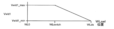
図14Bは、図14Aと合致する、2つのレベルの電圧が使用される場合の、ダミーワード線電圧のプロットを、選択ワード線位置の関数として示す。この場合、WLd1は、選択ワード線が位置するワード線の2つの可能なグループに基づく2つの可能なレベルを有する。第1のグループはWL0〜WLy−1を含み、第2のグループはWLy〜Wldsを含む。図14B〜図14Dにおいて、垂直軸は、1又は複数のドレイン側ダミーワード線のダミーワード線電圧Vwldを示す。水平軸は、NANDストリングに沿った選択ワード線(WLsel)位置を示す。例えば、これは、3Dメモリデバイスにおける高さである、z軸に沿った位置とすることができる。実線1410は、WL0≦WLsel<WLswitchのとき、Vwld1=Vwld1_maxである、及び、WLswitch≦WLsel≦WLdsのとき、Vwld1=Vwld1_minであることを示す。WLswitchは、異なるダミーワード線電圧に対するスイッチを示すワード線である。第1のダミーワード線に隣接し、これのドレイン側にある第2のダミーワード線の場合、破線1411は、WL0≦WLsel<WLswitchのとき、Vwld2=Vwld2_maxであり、WLswitch≦WLsel≦WLdsのとき、Vwld2=Vwld2_minであることを示す。さらに、1つの手法では、第1のダミーメモリセルに印加される電圧(Vwld1)のレベルは、選択ワード線と第1のダミーメモリセルとの間の距離に比例して第1の範囲で変化する(Vwld1_min〜Vwld1_max)。第2のダミーメモリセルに印加される電圧(Vwld2)のレベルは、該距離に比例して第2の範囲で変化し(Vwld2_min〜Vwld2_max)、第2の範囲は第1の範囲より小さい。一例として、Vwld1_max=5V、Vwld1_min=0V、Vwld2_max=4V、及びVwld2_min=2Vである。この例では、第2の範囲の最下部は第1の範囲の最下部より大きく、第2の範囲の最上部は第1の範囲の最上部より小さい。
FIG. 14B shows a plot of dummy word line voltage as a function of selected word line position when two levels of voltage are used, consistent with FIG. 14A. In this case, WLd1 has two possible levels based on two possible groups of word lines where the selected word line is located. The first group includes WL0 to WLy-1, and the second group includes WLy to Wlds. 14B to 14D, the vertical axis indicates the dummy word line voltage Vwld of one or more drain side dummy word lines. The horizontal axis indicates the selected word line (WLsel) position along the NAND string. For example, this can be a position along the z-axis, which is the height in a 3D memory device. A
最適なスイッチングワード線は、メモリデバイスの周囲温度などの要因によって影響され得る。例えば、温度が上昇すると、電子−ホール生成はより厳しくなるため、切り換えワード線はドレイン側から遠くに移動することになる。温度が低下すると、電子−ホール生成は厳しくなくなり、切り換えワード線はドレイン側のより近くに移動することになる。 The optimal switching word line can be affected by factors such as the ambient temperature of the memory device. For example, when the temperature rises, electron-hole generation becomes more severe, so that the switching word line moves far from the drain side. As the temperature drops, electron-hole generation becomes less severe and the switching word line moves closer to the drain side.
制御回路は、温度の関数として、第1のグループ及び第2のグループなどの2つの隣接グループ間の境界において切り換えワード線を規定するように構成されてよく、この場合、切り換えワード線は、温度が比較的低いとき、ドレイン側選択ゲートトランジスタに比較的近くなる。 The control circuit may be configured to define a switching word line as a function of temperature at a boundary between two adjacent groups, such as the first group and the second group, where the switching word line is a temperature Is relatively close to the drain side select gate transistor.
最適なスイッチングワード線は、ドレイン側からだけでなく、制御ゲートの長さ及び制御ゲート間の間隔などの要因から、生成された電子を完全に吸収するためにどの程度のワード線が利用可能であるかに左右される。一般的に、メモリデバイスが比較的少ないワード線を有する場合、制御ゲートの長さ及び制御ゲート間の間隔が比較的大きくなるのはより一般的である。例えば、WL30が図14Aにおいて最適な切り換えワード線であると仮定する。ホットキャリアを吸収するために利用可能なチャネルの長さを規定するドレイン側に17のワード線(WL31〜WL47)がある。切り換えワード線とドレイン側ダミーメモリセルとの間の距離は、17/48、又は、ワード線の総数の約1/3である。 The optimal switching word line is not only from the drain side, but also how many word lines can be used to completely absorb the generated electrons due to factors such as the length of the control gate and the spacing between the control gates. It depends on how it is. In general, when the memory device has relatively few word lines, it is more common for the length of the control gate and the spacing between the control gates to be relatively large. For example, assume that WL30 is the optimum switching word line in FIG. 14A. There are 17 word lines (WL31 to WL47) on the drain side that define the length of the channels available for absorbing hot carriers. The distance between the switching word line and the drain side dummy memory cell is 17/48, or about 1/3 of the total number of word lines.
第2の例として、24のみワード線があると仮定する。先の例にあるのと同じ制御ゲートの長さ及び制御ゲート間の間隔を仮定する場合、最適な切り換えワード線はおよそ24−17=WL7である可能性がある。切り換えワード線とドレイン側ダミーメモリセルとの間の距離は、17/24、又はワード線の総数の約2/3である。制御ゲートの長さ及び制御ゲート間の距離が先の例の場合よりも大きいと仮定する場合、最適な切り換えワード線はおよそWL8〜WL12である可能性がある。最適な切り換えワード線は、概算で、このソース側においてワード線の少なくとも約50%を含んでもよい。一般的に、最適な切り換えワード線はテストを行うことで判断可能である。 As a second example, assume that there are only 24 word lines. Assuming the same control gate length and spacing between control gates as in the previous example, the optimal switching word line could be approximately 24-17 = WL7. The distance between the switching word line and the drain side dummy memory cell is 17/24, or about 2/3 of the total number of word lines. Assuming that the length of the control gate and the distance between the control gates is greater than in the previous example, the optimal switching word line may be approximately WL8-WL12. An optimal switching word line may roughly include at least about 50% of the word lines on this source side. Generally, the optimum switching word line can be determined by performing a test.
図14Cは、図14Aと合致する、3つのレベルの電圧が使用される場合のダミーワード線電圧のプロットを、選択ワード線位置の関数として示す。ワード線の3つ以上のグループは、3つ以上の対応するダミーワード線電圧のレベルで規定されてよい。第1のグループでは、WL0≦WLsel<WLswitch1、及びVwld1=Vwld1_maxである。第2のグループでは、WLswitch1≦WLsel<WLswtich2、及びVwld1=Vwld1_intである。第3のグループでは、WLswitch2≦WLsel<WLds、及びVwld1=Vwld1_minである。2つ以上のグループを使用することによって、Vwld1の最高値と最低値との間の遷移がもたらされる。WLswitch1及びWLswitch2は、異なるダミーワード線電圧に対するスイッチを示すワード線である。 FIG. 14C shows a plot of dummy word line voltage as a function of selected word line position when three levels of voltage are used, consistent with FIG. 14A. Three or more groups of word lines may be defined with three or more corresponding dummy word line voltage levels. In the first group, WL0 ≦ WLsel <WLswitch1 and Vwld1 = Vwld1_max. In the second group, WLswitch1 ≦ WLsel <WLswitch2 and Vwld1 = Vwld1_int. In the third group, WLswitch2 ≦ WLsel <WLds and Vwld1 = Vwld1_min. Using more than one group results in a transition between the highest and lowest values of Vwld1. WLswitch1 and WLswitch2 are word lines indicating switches for different dummy word line voltages.
例えば、図14Aに基づいて、WLswitch1=WL30、及びWLswitch2=WL47としてよい。図14Aは、WL0〜WL30がエラー数がE1を下回る領域であり、WL31〜WL44が段階的な低下があり、エラー数がE2を超える領域であり、WL45〜WL47が突然の低下があり、エラー数が増大する領域であることを示す。 For example, WLswitch1 = WL30 and WLswitch2 = WL47 may be set based on FIG. 14A. In FIG. 14A, WL0 to WL30 are regions where the number of errors is less than E1, WL31 to WL44 are stepwise drops, the number of errors is greater than E2, and WL45 to WL47 are suddenly dropped and errors occur. Indicates that this is an area where the number increases.
図14Dは、図14Aと合致する、Vwld1が選択ワード線位置の関数として傾斜状に減少する場合のダミーワード線電圧のプロットを、選択ワード線位置の関数として示す。図14B及び図14Cにおいて、ダミーワード線電圧は、ステップ関数に従って、選択ワード線位置により変化する。 FIG. 14D shows a plot of the dummy word line voltage as a function of the selected word line position when Vwld1 decreases in a slope as a function of the selected word line position, consistent with FIG. 14A. 14B and 14C, the dummy word line voltage changes according to the selected word line position according to the step function.
この例では、WLd1は、選択ワード線位置のランプ関数又は他の関数に従って変化する。これによって、Vwld1の最高値と最低値との間で段階的な遷移がもたらされる。 In this example, WLd1 varies according to the ramp function or other function of the selected word line position. This provides a gradual transition between the highest and lowest values of Vwld1.
図15A〜図15Dは、異なるシナリオでの非選択NANDにおけるチャネル電圧(Vch)のプロットを示す。プリチャージ段階の後、及びVpgmが印加される直前のチャネル電圧が示される。垂直軸はVchを示し、水平軸はNANDストリングに沿った位置を示す。該位置は破線で区分され、ここで、隣接する破線間の領域は、トランジスタ/ワード線の真下のチャネル領域、又は、トランジスタ/ワード線間のチャネル領域に対応する。NANDストリングのドレイン側に焦点が置かれている。SGDはSGDトランジスタであり、WLd1は第1のダミーワード線であり、記載されている場合には、WLd2は第2のダミーワード線である。WLdsは第1のドレイン側データワード線であり、Wlds−1は第2のドレイン側データワード線であり、以下同様に続く。例えば、図9Aにおいて、WLds=WL22である。BLはビット線である。 15A-15D show plots of channel voltage (Vch) for unselected NAND in different scenarios. The channel voltage is shown after the precharge phase and just before Vpgm is applied. The vertical axis indicates Vch, and the horizontal axis indicates the position along the NAND string. The position is divided by a broken line, and a region between adjacent broken lines corresponds to a channel region directly below a transistor / word line or a channel region between transistors / word lines. The focus is on the drain side of the NAND string. SGD is an SGD transistor, WLd1 is a first dummy word line, and in the illustrated case WLd2 is a second dummy word line. WLds is the first drain-side data word line, Wlds-1 is the second drain-side data word line, and so on. For example, in FIG. 9A, WLds = WL22. BL is a bit line.
最初に述べられたように、プログラム電圧を印加する前のチャネルプリチャージ動作は、後続のプログラム電圧の間のブースト電位の上昇に寄与する。非選択NANDストリングにおけるチャネルブーストの大部分は、チャネル電圧がフローティングしている間の、ワード線からチャネルまでの容量結合に起因する。チャネル電圧をフローティングさせるために、選択ゲートトランジスタはオフされる(非導電にされる)。その後、ワード線は増大する。例えば、非選択ワード線電圧は0Vから8〜9Vまで増大する。選択ワード線電圧は、プログラムループに依存して、0Vから、例えば、15〜25VのVpgmまで増大する。チャネル電圧は、結合比(CR)で乗算されるワード線電圧の増加量(Vincrease)でブーストされる。例えば、Vch=Vinitial+(Vincrease×CR)である。Vinitialは、(例えば、図16A〜図16Eのt3における)ワード線電圧の増大前のチャネル電圧であり、例えば、0V、又はプリチャージ動作から生じる1〜2Vなどの小さい値とすることができる。よって、より大きいVinitialはより大きいVchをもたらす。Vchは、(例えば、図16A〜図16Eのt4における)Vpgmが印加されるときの最終チャネルブーストレベルである。 As stated initially, the channel precharge operation before applying the program voltage contributes to the boost potential rise during the subsequent program voltage. Most of the channel boost in unselected NAND strings is due to capacitive coupling from the word line to the channel while the channel voltage is floating. In order to float the channel voltage, the select gate transistor is turned off (made non-conductive). Thereafter, the word lines increase. For example, the unselected word line voltage increases from 0V to 8-9V. The selected word line voltage increases from 0 V to, for example, 15 to 25 V Vpgm depending on the program loop. The channel voltage is boosted by the increase (Vincrease) of the word line voltage multiplied by the coupling ratio (CR). For example, Vch = Vinitial + (Vincrease × CR). Initial is a channel voltage before the increase of the word line voltage (for example, at t3 in FIGS. 16A to 16E), and may be a small value such as 0 V or 1 to 2 V resulting from the precharge operation, for example. Thus, a larger Vinyl results in a larger Vch. Vch is the final channel boost level when Vpgm is applied (eg, at t4 in FIGS. 16A-16E).
チャネルプリチャージ動作は、チャネルにおける残留電子、ひいてはブーストチャネル電位の除去に寄与する。プリチャージ効率、例えば、プリチャージの使用によるチャネル電位増加の増大を制御するために、ドレイン側ダミーワード線に加えるバイアスを調節することができる。一般的に、ダミーメモリセルの制御ゲート/ワード線電圧が高い場合、ダミーメモリセルは完全にオンにされ、残留電子は完全に取り除かれ得る。結果として、プリチャージ動作の終了におけるチャネル電位(Vinitial)は高く、ブーストは改善される。しかしながら、ダミーワード線電圧が0Vから5Vなどの高いレベルに変更された場合、より低いワード線、例えば、NANDストリングのソース側により近いワード線のチャネルブーストは改善したが、より高いワード線、例えば、NANDストリングのドレイン側により近いワード線のチャネルブーストは著しく低下した。チャネルブーストの量は、プログラミング後にデータをリードバックするとき、Er〜A状態の読出しエラーに関して測定してもよい。 The channel precharge operation contributes to the removal of residual electrons in the channel and thus boost channel potential. The bias applied to the drain side dummy word line can be adjusted to control the precharge efficiency, for example, the increase in channel potential increase due to the use of precharge. In general, if the control gate / word line voltage of the dummy memory cell is high, the dummy memory cell is fully turned on and the residual electrons can be completely removed. As a result, the channel potential (Vinitial) at the end of the precharge operation is high and the boost is improved. However, if the dummy word line voltage is changed to a high level such as 0V to 5V, the channel boost of lower word lines, eg, word lines closer to the source side of the NAND string, improved, but higher word lines, eg The channel boost of the word line closer to the drain side of the NAND string was significantly reduced. The amount of channel boost may be measured in terms of Er to A state read errors when data is read back after programming.
チャネルブーストの低下は、ポリシリコンチャネルにおけるホットキャリアの生成を容易にするNANDストリングのドレイン側において、段階的なチャネルブーストによって生じる。プリチャージ効率(残留電子を取り除く能力)とホットキャリア生成効率との間に競合がある。より低いワード線について、消去状態にある選択ワード線のドレイン側における多くのワード線/メモリセルの存在によって、合計のチャネル静電容量が大きくなるため、ホットキャリアを容易に吸収可能であり、プリチャージ向上の利点はより際立つ。しかし、より高いワード線について、選択ワード線のドレイン側におけるチャネル静電容量が小さくなることによって、ホットキャリア誘導のブースト低下がより際立つ。よって、最上部(ドレイン側)のワード線のプログラムディスターブは悪化する。本明細書に提供される技術はこの問題点に対処する。 The decrease in channel boost is caused by a gradual channel boost on the drain side of the NAND string that facilitates hot carrier generation in the polysilicon channel. There is a competition between precharge efficiency (ability to remove residual electrons) and hot carrier generation efficiency. For lower word lines, the presence of many word lines / memory cells on the drain side of the selected word line in the erased state increases the total channel capacitance, so that hot carriers can be easily absorbed and pre-charged. The benefits of improved charge are more pronounced. However, for higher word lines, the decrease in channel capacitance on the drain side of the selected word line makes the hot carrier induced boost drop more pronounced. Therefore, the program disturb of the uppermost (drain side) word line deteriorates. The techniques provided herein address this issue.
図15Aは、1つのドレイン側ダミーメモリセルが使用される、図14Aのプロット1400と合致する、WLselがドレイン側ダミーメモリセルから比較的離れており、Wld1=高である場合の、非選択NANDストリングにおけるチャネル電圧のプロットを示す。Vchは約10Vであってよい。
FIG. 15A shows a non-selected NAND where WLsel is relatively far from the drain side dummy memory cell and Wld1 = high, consistent with
上述の式、Vch=Vinitial+(Vincrease×CR)を使用して、例えば、2Vの、正のビット線プリチャージ電圧がビット線から選択ワード線までのチャネルを容易に通過できることを想起されたい。従って、Vinitial=2Vである。さらに、プリチャージ段階後に非選択ワード線が0Vから8vまで増大すると、簡略化のためにCR=1と仮定すると、Vincrease=8Vとなる。よって、データワード線下のチャネル部分では、Vch=2+8×1=10Vである。Wld1下のチャネルでは、非選択NANDストリングについて、プリチャージ段階において、及びVpgmが印加されるとき、Vwld1=5Vと仮定する。よって、容量結合によってWLd1下のVchを増大させるVwld1の増大はない。WLd1下のチャネル部分は約2Vのままである。これによって、電子(e)−正孔(h)対を生成する大きい勾配1510がもたらされる。電子はデータワード線に向かって移動し、ホールは反対方向に向かって移動する。既述したように、電子正孔対が生成されても、チャネルによって吸収可能であり、データワード線のプログラムディスターブが生じることはない。
Recall that using the above equation, Vch = Vinitial + (Vincrease × CR), a positive bit line precharge voltage of, for example, 2V can easily pass through the channel from the bit line to the selected word line. Therefore, Initial = 2V. Furthermore, if the non-selected word line increases from 0V to 8v after the precharge stage, assuming that CR = 1 for simplicity, Vincrease = 8V. Therefore, Vch = 2 + 8 × 1 = 10 V in the channel portion below the data word line. For the channel under Wld1, assume that Vwld1 = 5V for the unselected NAND string, in the precharge phase, and when Vpgm is applied. Therefore, there is no increase in Vwld1 that increases Vch under WLd1 by capacitive coupling. The channel portion under WLd1 remains at about 2V. This results in a
図15Bは、1つのドレイン側ダミーメモリセルが使用される、図14Aのプロット1401と合致する、WLselがドレイン側ダミーメモリセルに比較的近く、Wld1=低である場合の、非選択NANDストリングにおけるチャネル電圧のプロットを示す。この場合、Vwld1は、ダミーメモリセルが相対的に非導電状態であるように低い。これは、ビット線のプリチャージのほとんどがチャネルに達することを阻止するが、少量のプリチャージはチャネルに進入してもよい。この結果、図15AのようなVch=10Vの代わりに、Vch=8〜9Vになる。Wld1下のチャネル部分では、Wld1下のVchを増大させる、例えば、0Vから5VまでのVwld1の増大がある。従って、WLd1下のチャネル部分は、図15Aにあるような2Vの代わりに約7Vになる。SGDトランジスタは、2VのプリチャージがSGD下のチャネル部分まで通過するように、図15Aにあるように導電性を有する。SGDの制御ゲートは、プリチャージ後に、例えば、導電状態から非導電状態まで減少して、チャネルをフローティングさせ、ワード線電圧の増大によってVpgmが印加される前により高くブーストされるのを許容する。
FIG. 15B is in a non-selected NAND string where one drain-side dummy memory cell is used, and WLsel is relatively close to the drain-side dummy memory cell and Wld1 = low, consistent with
図15Cは、2つのドレイン側ダミーメモリセルが使用される、図14Aのプロット1400と合致する、WLselがドレイン側ダミーメモリセルから比較的離れており、Wld1=高及びWld2=高である場合の、非選択NANDストリングにおけるチャネル電圧のプロットを示す。複数のドレイン側ダミーワード線は、チャネル勾配を低減する、WLd1とSGDとの間のより広い遷移領域をもたらすために使用してもよい。図15Aにあるように、e−h対を生成する、WLd1とWLd2との間に著しいチャネル勾配があるが、電子は、プログラムディスターブが生じる前に吸収可能である。
FIG. 15C shows that when two drain side dummy memory cells are used, WLsel is relatively far from the drain side dummy memory cell, consistent with
図15Dは、2つのドレイン側ダミーメモリセルが使用される、図14Aのプロット1401と合致する、WLselがドレイン側ダミーメモリセルに比較的近く、Wld1=低及びWld2=低である場合の、非選択NANDストリングにおけるチャネル電圧のプロットを示す。この場合、Vwld1は低いため、ビット線のプリチャージのほとんどがチャネルに達することを阻止される。この結果、図15CにあるようなVch=10Vの代わりに、Vch=8〜9Vになる。図15Bにあるように、WLd1下のチャネル部分は約7Vであり、SGDトランジスタ下のチャネル部分は2Vである。Vwld2はプリチャージ段階の間、例えば、2Vであってよく、プリチャージ段階の後でありVpgmが印加される前に、4Vまで増大する。これによって、合計4VのVchに対して、2Vのプリチャージの上に4−2=2Vのチャネルブーストが生じる。
FIG. 15D shows that non-drain when two drain side dummy memory cells are used, WLsel is relatively close to the drain side dummy memory cell, and Wld1 = low and Wld2 = low, consistent with
図16A〜図16Eは、例示的な波形を示す。垂直軸は電圧であり、水平軸は、プログラムループのプログラム部分における時間の増大を表す。t1〜t3の期間はプリチャージ段階である。t3〜t4の期間は、ワード線電圧が増大するさらなるブースト段階である。t4〜t5の期間は、Vpgmが印加されるプログラミング段階である。t5〜t6及びそれ以降の期間は、プログラムループのプログラミング部分が完了される完了段階である。その後、図示されないベリファイ段階は、1又は複数のベリファイテストを行うために使用されてもよい。 16A-16E illustrate exemplary waveforms. The vertical axis is voltage and the horizontal axis represents the increase in time in the program part of the program loop. The period from t1 to t3 is a precharge stage. The period from t3 to t4 is a further boost stage in which the word line voltage increases. The period from t4 to t5 is a programming stage in which Vpgm is applied. The period from t5 to t6 and the subsequent period is a completion stage in which the programming part of the program loop is completed. Thereafter, a verify step (not shown) may be used to perform one or more verify tests.
図16Aは、図10と合致する、選択NANDストリングに対するBLsel(プロット1600)、及び非選択NANDストリングに対するBLunsel(プロット1601)を含む、プログラミング動作における時間関数として例示的なビット線電圧を示す。ビット線電圧(Vbl)はt1〜t2の間に2Vといったプリチャージレベルに設定される。非選択NANDストリングに対して、t3〜t6で、Vblは2V又は同様のレベルを維持する。これによって、SGDトランジスタは、チャネル電圧をフローティングさせ、t3〜t4で容量結合によってさらなるブーストを可能にするために、導電状態から非導電状態まで移行することになる。非選択NANDストリングのメモリセルはプログラミングから阻止される。t6の後、Vblは0Vに戻る。選択NANDストリングについて、t3〜t6で、Vblは、選択NANDストリングにおける選択メモリセルのプログラミングを可能にするために、0V又は同様のレベルを維持する。これによって、SGDトランジスタは導電状態を維持する。 FIG. 16A shows exemplary bit line voltages as a function of time in programming operations, including BLsel (plot 1600) for selected NAND strings and BLunsel (plot 1601) for unselected NAND strings, consistent with FIG. The bit line voltage (Vbl) is set to a precharge level of 2V between t1 and t2. For unselected NAND strings, from t3 to t6, Vbl maintains 2V or a similar level. This causes the SGD transistor to transition from a conducting state to a non-conducting state in order to float the channel voltage and allow further boost by capacitive coupling from t3 to t4. Memory cells of unselected NAND strings are blocked from programming. After t6, Vbl returns to 0V. For the selected NAND string, from t3 to t6, Vbl maintains 0V or a similar level to allow programming of the selected memory cell in the selected NAND string. As a result, the SGD transistor maintains a conductive state.
図16Bは、図10と合致する、例示的なSGD電圧(ドレイン側選択ゲートトランジスタの電圧)をプログラミング動作(プロット1610)における時間関数として示す。Vsgdは、t1〜t2の間、4Vなどのプリチャージレベルに設定される。t3〜t6で、Vsgdを、2Vなどのレベル又は同様のレベルに低下させる。1つの例では、選択NANDストリング及び非選択NANDストリングは、共通のSGD線を有し、それぞれのNANDストリングは別個のビット線を有する。よって、t3〜t6で、Vblは非選択NANDストリングに対して(Vsgd−Vth<Vblの)非導電状態でのそれぞれのSGDトランジスタを設けるために高く、又は、非選択NANDストリングに対して(Vsgd−Vth>Vblの)導電状態でのそれぞれのSGDトランジスタを設けるために低く設定してもよい。SGDトランジスタのVthの一例は2Vである。t6の後、Vsgdは0Vに戻る。これによって、SGDトランジスタは全てのNANDストリングに対して非導電状態に移行することになる。 FIG. 16B shows an exemplary SGD voltage (drain side select gate transistor voltage), consistent with FIG. 10, as a function of time in a programming operation (plot 1610). Vsgd is set to a precharge level such as 4 V from t1 to t2. From t3 to t6, Vsgd is lowered to a level such as 2V or similar. In one example, the selected NAND string and the unselected NAND string have a common SGD line, and each NAND string has a separate bit line. Thus, from t3 to t6, Vbl is high to provide each SGD transistor in the non-conductive state (Vsgd−Vth <Vbl) for the non-selected NAND string, or (Vsgd It may be set low to provide each SGD transistor in the conductive state (-Vth> Vbl). An example of Vth of the SGD transistor is 2V. After t6, Vsgd returns to 0V. This causes the SGD transistor to transition to a non-conductive state for all NAND strings.
図16Cは、図10と合致する、WLd1からWLselまでの距離が比較的遠い(プロット1620)又は比較的近い(プロット1621)場合の例示的なWLd1(第1のドレイン側ダミーワード線の電圧)を、プログラミング動作における時間関数として示す。t1〜t3で、距離が比較的遠い場合、WLd1は高レベル、例えば5Vに設定され、距離が比較的近い場合、WLd1は低レベル、例えば0Vに設定される。t3〜t6で、WLd1は、近距離又は遠距離に対して高レベルに設定してもよい。 FIG. 16C is an exemplary WLd1 (first drain side dummy word line voltage) when the distance from WLd1 to WLsel is relatively far (plot 1620) or relatively close (plot 1621), consistent with FIG. Is shown as a function of time in the programming operation. When the distance is relatively long from t1 to t3, WLd1 is set to a high level, for example, 5V, and when the distance is relatively close, WLd1 is set to a low level, for example, 0V. From t3 to t6, WLd1 may be set to a high level for a short distance or a long distance.
図16Dは、例示的なWLunsel(非選択ワード線の電圧)(プロット1630)をプログラミング動作における時間関数として示す。WLunselは、t3〜t4において、0Vなどの低レベルから8〜9Vなどのパス電圧まで増大し、t4〜t5でそのレベルを維持した後、0Vに戻る。 FIG. 16D shows an exemplary WLunsel (voltage of unselected word lines) (plot 1630) as a function of time in a programming operation. WLunsel increases from a low level such as 0 V to a pass voltage such as 8 to 9 V from t3 to t4, and maintains that level from t4 to t5, and then returns to 0 V.
図16Eは、例示的なWLsel(選択ワード線の電圧)(プロット1640)をプログラミング動作における時間関数として示す。WLselは、t3〜t4において、0Vなどの低レベルから15〜25Vなどのプログラム電圧(Vpgm)まで増大し、t4〜t5でそのレベルを維持した後、0Vに戻る。 FIG. 16E shows an exemplary WLsel (voltage of selected word line) (plot 1640) as a function of time in a programming operation. WLsel increases from a low level such as 0 V to a program voltage (Vpgm) such as 15 to 25 V from t3 to t4, and maintains that level from t4 to t5, and then returns to 0 V.
したがって、1つの実施形態では、メモリデバイスは、選択NANDストリングと非選択NANDストリングとを含む複数のNANDストリングであって、選択NANDストリングは選択メモリセルと非選択メモリセルとを含む複数のメモリセルを含み、非選択NANDストリングは選択メモリセルに対応する非選択メモリセルと残りの非選択メモリセルとを含む複数のメモリセルを含み、複数のNANDストリングの各NANDストリングは、それぞれのチャネルと、ドレイン側選択ゲートトランジスタと、第1のダミーメモリセルとを含み、第1のダミーメモリセルは複数のメモリセルのドレイン側選択ゲートトランジスタとドレイン端メモリセルとの間にあり、複数のNANDストリングの各NANDストリングは複数のビット線のビット線それぞれに接続され、選択メモリセル及び選択メモリセルに対応する非選択メモリセルは、複数のワード線の中の選択ワード線に接続され、選択NANDストリングの非選択メモリセル及び非選択NANDストリングの残りの非選択メモリセルは、複数のワード線の中の非選択ワード線に接続される、複数のNANDストリングと、制御回路と、を含むことが分かる。制御回路は、非選択NANDストリングに対して、プログラミング動作において選択ワード線にプログラム電圧を印加する前にプリチャージ動作を実行するように構成され、プリチャージ動作を実行するために、制御回路は、非選択NANDストリングのビット線それぞれへの正のプリチャージ電圧と、第1のダミーメモリセルへの電圧と、を同時に印加するように構成され、第1のダミーメモリセルに印加された電圧のレベルは、選択ワード線と第1のダミーメモリセルとの間の距離の関数であり、それによって、距離が大きくなる場合にこのレベルが高くなる。 Accordingly, in one embodiment, the memory device is a plurality of NAND strings including a selected NAND string and an unselected NAND string, wherein the selected NAND string is a plurality of memory cells including a selected memory cell and an unselected memory cell. The non-selected NAND string includes a plurality of memory cells including a non-selected memory cell corresponding to the selected memory cell and the remaining non-selected memory cells, each NAND string of the plurality of NAND strings including a respective channel; A drain side select gate transistor and a first dummy memory cell, wherein the first dummy memory cell is between the drain side select gate transistor and the drain end memory cell of the plurality of memory cells, and Each NAND string has multiple bit line bites. A non-selected memory cell corresponding to the selected memory cell and a non-selected memory cell corresponding to the selected memory cell is connected to a selected word line of the plurality of word lines, and the non-selected memory cell and the non-selected NAND string of the selected NAND string It can be seen that the remaining unselected memory cells include a plurality of NAND strings connected to the unselected word lines of the plurality of word lines and a control circuit. The control circuit is configured to perform a precharge operation on the unselected NAND string before applying a program voltage to the selected word line in the programming operation, and in order to perform the precharge operation, the control circuit includes: A level of the voltage applied to the first dummy memory cell is configured to simultaneously apply a positive precharge voltage to each bit line of the unselected NAND string and a voltage to the first dummy memory cell. Is a function of the distance between the selected word line and the first dummy memory cell, whereby this level increases as the distance increases.
別の実施形態では、メモリデバイスにおいてプログラミングするための方法は、非選択NANDストリングに対して、選択NANDストリングにおける選択メモリセルに対するプログラミング動作中に、選択メモリセルが選択ワード線に接続される場合に、非選択NANDストリングのビット線それぞれへの正のプリチャージ電圧と、非選択NANDストリングの第1のメモリセルへの電圧と、を同時に印加することによってプリチャージ動作を実行する工程であって、第1のダミーメモリセルに印加される電圧のレベルは、選択ワード線と第1のダミーメモリセルとの間の距離の関数であり、それによって、距離が大きくなる場合にレベルが高くなり、第1のダミーメモリセルは、非選択NANDストリングの複数のメモリセルのドレイン側選択ゲートトランジスタとドレイン端メモリセルとの間にある、プリチャージを実行する工程と、プリチャージ動作後に、選択ワード線にプログラム電圧を印加する工程とを含む。 In another embodiment, a method for programming in a memory device is for a non-selected NAND string when the selected memory cell is connected to a selected word line during a programming operation for the selected memory cell in the selected NAND string. Performing a precharge operation by simultaneously applying a positive precharge voltage to each bit line of the unselected NAND string and a voltage to the first memory cell of the unselected NAND string, The level of the voltage applied to the first dummy memory cell is a function of the distance between the selected word line and the first dummy memory cell, so that the level increases as the distance increases, One dummy memory cell is a drain of a plurality of memory cells of an unselected NAND string. It lies between the selection gate transistor and the drain end memory cells, and performing a precharge after the precharge operation, and a step of applying a program voltage to the selected word line.
別の実施形態では、メモリデバイスは、上述した方法における工程のそれぞれを実行するための手段を含む。 In another embodiment, the memory device includes means for performing each of the steps in the method described above.
別の実施形態では、メモリデバイスは、選択NANDストリングと非選択NANDストリングとを含む複数のNANDストリングであって、選択NANDストリングは選択メモリセルと非選択メモリセルとを含む複数のメモリセルを含み、非選択NANDストリングは選択メモリセルに対応する非選択メモリセルと残りの選択メモリセルとを含む複数のメモリセルを含み、複数のNANDストリングの各NANDストリングは、それぞれのチャネルと、ドレイン側選択ゲートトランジスタと、第1のダミーメモリセルとを含み、第1のダミーメモリセルは複数のメモリセルのドレイン側選択ゲートトランジスタとドレイン端メモリセルとの間にあり、複数のNANDストリングの各NANDストリングは複数のビット線のビット線それぞれに接続され、選択メモリセル及び選択メモリセルに対応する非選択メモリセルは、複数のワード線の中の選択ワード線に接続され、選択NANDストリングの非選択メモリセル及び非選択NANDストリングの残りの非選択メモリセルは、複数のワード線の中の非選択ワード線に接続される、複数のNANDストリングと、制御回路と、を含む。制御回路は、非選択NANDストリングに対して、プログラミング動作において選択ワード線にプログラム電圧を印加する前にプリチャージ動作を実行するように構成され、プリチャージ動作を実行するために、制御回路は、非選択NANDストリングのビット線それぞれに正のプリチャージ電圧を同時に印加するように、及び、第1のダミーメモリセルを制御して、ビット線それぞれからそれぞれのチャネルまで通じる正のプリチャージ電圧の量を制御するように構成され、その量は、選択ワード線と第1のダミーメモリセルとの間の距離の関数であり、それによって、距離が大きくなる場合に量が多くなる。 In another embodiment, the memory device is a plurality of NAND strings including a selected NAND string and an unselected NAND string, the selected NAND string including a plurality of memory cells including selected memory cells and unselected memory cells. The non-selected NAND string includes a plurality of memory cells including a non-selected memory cell corresponding to the selected memory cell and the remaining selected memory cells, and each NAND string of the plurality of NAND strings has a respective channel and drain side selected. Each of the plurality of NAND strings includes a gate transistor and a first dummy memory cell, the first dummy memory cell being between the drain-side selection gate transistor and the drain end memory cell of the plurality of memory cells. Is for each bit line of multiple bit lines The selected memory cell and the non-selected memory cell corresponding to the selected memory cell are connected to the selected word line of the plurality of word lines, and the non-selected memory cell of the selected NAND string and the remaining non-selected memory cell of the non-selected NAND string are connected. The selected memory cell includes a plurality of NAND strings connected to an unselected word line among the plurality of word lines, and a control circuit. The control circuit is configured to perform a precharge operation on the unselected NAND string before applying a program voltage to the selected word line in the programming operation, and in order to perform the precharge operation, the control circuit includes: The amount of positive precharge voltage that passes from each bit line to each channel by simultaneously applying a positive precharge voltage to each bit line of the unselected NAND string and controlling the first dummy memory cell. The amount is a function of the distance between the selected word line and the first dummy memory cell, so that the amount increases as the distance increases.
本発明の前述の詳細な説明は、例示及び説明の目的で提示されており、網羅的である又は開示された正確な形態に本発明を限定することは意図されない。上記の教示を考慮して、多くの修正及び変形が可能である。説明した実施形態は、本発明の原理及びその実用的応用を最も良く説明するために、それによって、当業者が、様々な実施形態において及び考えられる特定の使用に適するような様々な修正によって本発明を最も良く活用することができるように、選定されたものである。本発明の範囲は添付の特許請求の範囲によって定められていることが意図される。 The foregoing detailed description of the invention has been presented for purposes of illustration and description, and is not intended to be exhaustive or to limit the invention to the precise form disclosed. Many modifications and variations are possible in view of the above teachings. The described embodiments are described in order to best explain the principles of the invention and its practical application so that those skilled in the art can modify the embodiments and various modifications as appropriate for the particular use envisaged. It was chosen so that the invention could be best utilized. It is intended that the scope of the invention be defined by the appended claims.
本発明の前述の詳細な説明は、例示及び説明の目的で提示されており、網羅的である又は開示された正確な形態に本発明を限定することは意図されない。上記の教示を考慮して、多くの修正及び変形が可能である。説明した実施形態は、本発明の原理及びその実用的応用を最も良く説明するために、それによって、当業者が、様々な実施形態において及び考えられる特定の使用に適するような様々な修正によって本発明を最も良く活用することができるように、選定されたものである。本発明の範囲は添付の特許請求の範囲によって定められていることが意図される。
以下の項目は、国際出願時の特許請求の範囲に記載の要素である。
[項目1]
選択NANDストリングと非選択NANDストリングとを含む複数のNANDストリング(NS1、NS2、NS0_SBa、NS0_SBb、NS0_SBc、NS0_SBd)であって、
前記選択NANDストリングは、選択メモリセル(921)と、非選択メモリセルと、を含む複数のメモリセル(300、333、…、334及び335、400、433、…、434及び435)を含み、
前記非選択NANDストリングは、前記選択メモリセル(921)に対応する非選択メモリセル(961)と、残りの非選択メモリセルと、を含む複数のメモリセルを含み、
前記複数のNANDストリングの各NANDストリングは、それぞれのチャネル(406、665)と、ドレイン側選択ゲートトランジスタ(680、681、817、818、837、838、857、858、877、878、901、941、902、942)と、第1のダミーメモリセル(815、835、855、875、904、944)と、を含み、
前記第1のダミーメモリセルは、前記複数のメモリセルの前記ドレイン側選択ゲートトランジスタとドレイン端メモリセル(814、834、854、874、905、945)との間にあり、
前記複数のNANDストリングの各NANDストリングは複数のビット線(BL0、BL0A、BL0A−1)のビット線それぞれに接続され、
前記選択メモリセル及び前記選択メモリセルに対応する前記非選択メモリセルは、複数のワード線(WL0〜WL22)の中の選択ワード線に接続され、
前記選択NANDストリングの前記非選択メモリセル及び前記非選択NANDストリングの前記残りの非選択メモリセルは、前記複数のワード線の中の非選択ワード線に接続される、前記複数のNANDストリングと、
前記非選択NANDストリングに対して、プログラミング動作において前記選択ワード線にプログラム電圧を印加する前にプリチャージ動作を実行するように構成される制御回路(110、112、114、116、122、128、132)であって、前記プリチャージ動作を実行するために、前記制御回路は、前記非選択NANDストリングの前記ビット線それぞれへの正のプリチャージ電圧と、前記第1のダミーメモリセルへの電圧と、を同時に印加するように構成され、前記第1のダミーメモリセルに印加された前記電圧のレベル(WLd1)は、前記選択ワード線と前記第1のダミーメモリセルとの間の距離の関数であり、それによって、前記距離が大きくなる場合に前記レベルが高くなる、前記制御回路と、
を備える、メモリデバイス。
[項目2]
前記距離の前記関数に従って、前記制御回路は、前記選択ワード線が前記複数のワード線の第1のグループのワード線(WL0〜WLy−1)の中にある場合の第1の値において、及び、前記選択ワード線が前記複数のワード線の第2のグループのワード線(WLy〜WLds)の中にある場合の、前記第1の値よりも小さい第2の値において、前記第1のダミーメモリセルに印加される前記電圧の前記レベルを提供するように構成され、
前記第1のグループのワード線は前記複数のワード線の50〜80%を含み、
前記第2のグループのワード線は前記複数のワード線の残りを含む、項目1に記載のメモリデバイス。
[項目3]
前記制御回路は、温度の関数として、前記第1のグループ(WL0〜WLy−1)と前記第2のグループ(WLy〜WLds)との間の境界において切り換えワード線(WLswitch)を規定するように構成され、
前記切り換えワード線は、前記温度が比較的低い場合に、前記ドレイン側選択ゲートトランジスタに比較的近くなる、項目2に記載のメモリデバイス。
[項目4]
前記距離の前記関数に従って、前記制御回路は、前記選択ワード線が前記複数のワード線の第1のグループのワード線の中にある場合の第1の値において、及び、前記選択ワード線が前記複数のワード線の第2のグループのワード線の中にある場合の、前記第1の値よりも小さい第2の値において、前記第1のダミーメモリセルに印加される前記電圧の前記レベルを提供するように構成され、
前記第1のグループにおける前記選択ワード線と、前記第1のダミーメモリセルとの間の距離は、前記第2のグループにおける前記選択ワード線と、前記第1のダミーメモリセルとの間の距離よりも大きい、項目1に記載のメモリデバイス。
[項目5]
前記距離の前記関数に従って、前記制御回路は、前記選択ワード線が前記複数のワード線の第3のグループのワード線の中にある場合の、前記第2の値よりも小さい第3の値において、前記第1のダミーメモリセルに印加される前記電圧の前記レベルを提供するように構成され、
前記第2のグループにおける前記選択ワード線と、前記第1のダミーメモリセルとの間の距離は、前記第3のグループにおける前記選択ワード線と、前記第1のダミーメモリセルとの間の距離よりも大きい、項目4に記載のメモリデバイス。
[項目6]
前記距離が最大である場合に、前記第1のダミーメモリセルに印加される前記電圧の前記レベルが前記第1のダミーメモリセルの閾値電圧よりも大きい、項目1から5のいずれか一項に記載のメモリデバイス。
[項目7]
前記距離が最小である場合に、前記第1のダミーメモリセルに印加される前記電圧の前記レベルが前記第1のダミーメモリセルの閾値電圧よりも小さい、項目1から6のいずれか一項に記載のメモリデバイス。
[項目8]
前記第1のダミーメモリセルは前記複数のワード線の中のドレイン側データワード線に隣接しており、
前記複数のNANDストリングのそれぞれのNANDストリングは、前記第1のダミーメモリセルと、前記第1のダミーメモリセルに隣接する前記ドレイン側選択ゲートトランジスタとの間に第2のダミーメモリセル(816、836、856、876、903、943)を含み、
前記制御回路は、前記第1のダミーメモリセルに前記電圧が印加されるのと同時に、前記第2のダミーメモリセルに電圧を印加するように構成され、
前記第1のダミーメモリセルに印加される前記電圧の前記レベルは前記距離に比例して第1の範囲で変化し、
前記第2のダミーメモリセルに印加される前記電圧のレベルは、前記距離に比例して第2の範囲で変化し、
前記第2の範囲は前記第1の範囲よりも小さい、項目1から7のいずれか一項に記載のメモリデバイス。
[項目9]
前記第2の範囲の最下部(Vwld2_min)は前記第1の範囲の最下部(Vwld1_min)よりも大きく、
前記第2の範囲の最上部(Vwld2_max)は前記第1の範囲の最上部(Vwld1_max)よりも小さい、項目8に記載のメモリデバイス。
[項目10]
前記非選択NANDストリングに対して、前記制御回路は、前記ドレイン側選択ゲートトランジスタを、前記電圧が前記第1のダミーメモリセルに印加されるのと同時に導電状態にし、及び、前記プログラム電圧の印加と同時に非導電状態にするように構成され、
前記選択NANDストリングに対して、前記制御回路は、前記電圧が前記第1のダミーメモリセルに印加されるのと同時に、前記ドレイン側選択ゲートトランジスタを導電状態にし、前記ビット線それぞれに0Vを印加するように構成される、項目1から9のいずれか一項に記載のメモリデバイス。
[項目11]
前記メモリデバイスは、前記複数のワード線がスタックの異なる層に配置され、前記チャネルが前記スタックにおいて垂直に延在する3次元積層メモリデバイスを含む、項目1から10のいずれか一項に記載のメモリデバイス。
[項目12]
前記非選択NANDストリングは、ソース側選択ゲートトランジスタを含み、
前記非選択NANDストリングにおいて、前記プリチャージ動作中、前記選択ワード線と前記第1のダミーメモリセルとの間の非選択メモリセルは消去状態にあり、
前記選択ワード線と前記ソース側選択ゲートトランジスタとの間の非選択メモリセルはプログラム状態にある、項目1から11のいずれか一項に記載のメモリデバイス。
[項目13]
メモリデバイスにおいてプログラミングするための方法であって、
非選択NANDストリング(NS1、NS2、NS0_SBa、NS0_SBb、NS0_SBc、NS0_SBd)に対して、選択NANDストリングにおける選択メモリセル(921)に対するプログラミング動作中に、前記選択メモリセルが選択ワード線(WL0〜WL22)に接続される場合に、前記非選択NANDストリングのビット線それぞれ(BL0、BL0A、BL0A−1)への正のプリチャージ電圧と、前記非選択NANDストリングの第1のダミーメモリセル(815、835、855、875、904、944)への電圧と、を同時に印加することによってプリチャージ動作を実行する工程であって、前記第1のダミーメモリセルに印加される前記電圧のレベルは、選択ワード線と前記第1のダミーメモリセルとの間の距離の関数であり、それによって、前記距離が大きくなる場合に前記レベルが高くなり、前記第1のダミーメモリセルは、前記非選択NANDストリングの複数のメモリセルのドレイン側選択ゲートトランジスタ(680、681、817、818、837、838、857、858、877、878、901、941、902、942)とドレイン端メモリセル(814、834、854、874、905、945)との間にある、前記プリチャージ動作を実行する工程と、
前記プリチャージ動作後に、前記選択ワード線にプログラム電圧を印加する工程と、
を含む、方法。
[項目14]
前記プログラミング動作において、複数のプログラムループの各プログラムループ(PL)において、前記プリチャージ動作を行う工程と、前記プログラム電圧を前記選択ワード線に印加する工程と、を繰り返す工程をさらに含む、項目13に記載の方法。
[項目15]
前記第1のダミーメモリセルに印加される前記電圧の前記レベルは、前記選択ワード線が複数のワード線の第1のグループのワード線の中にある場合に第1の値であり、前記選択ワード線が前記複数のワード線の第2のグループのワード線の中にある場合に前記第1の値よりも小さい第2の値であり、
前記第1のグループのワード線は前記複数のワード線の50〜75%を含み、
前記第2のグループのワード線は前記複数のワード線の残りを含む、項目13又は14に記載の方法。
The foregoing detailed description of the invention has been presented for purposes of illustration and description, and is not intended to be exhaustive or to limit the invention to the precise form disclosed. Many modifications and variations are possible in view of the above teachings. The described embodiments are described in order to best explain the principles of the invention and its practical application so that those skilled in the art can modify the embodiments and various modifications as appropriate for the particular use envisaged. It was chosen so that the invention could be best utilized. It is intended that the scope of the invention be defined by the appended claims.
The following items are the elements described in the claims at the time of international application.
[Item 1]
A plurality of NAND strings (NS1, NS2, NS0_SBa, NS0_SBb, NS0_SBc, NS0_SBd) including a selected NAND string and a non-selected NAND string,
The selected NAND string includes a plurality of memory cells (300, 333,..., 334 and 335, 400, 433,..., 434 and 435) including a selected memory cell (921) and an unselected memory cell,
The unselected NAND string includes a plurality of memory cells including an unselected memory cell (961) corresponding to the selected memory cell (921) and the remaining unselected memory cells.
Each NAND string of the plurality of NAND strings includes a channel (406, 665) and a drain side select gate transistor (680, 681, 817, 818, 837, 838, 857, 858, 877, 878, 901, 941). , 902, 942), and first dummy memory cells (815, 835, 855, 875, 904, 944),
The first dummy memory cell is between the drain side select gate transistor and the drain end memory cells (814, 834, 854, 874, 905, 945) of the plurality of memory cells,
Each NAND string of the plurality of NAND strings is connected to a bit line of a plurality of bit lines (BL0, BL0A, BL0A-1),
The selected memory cell and the non-selected memory cell corresponding to the selected memory cell are connected to a selected word line among a plurality of word lines (WL0 to WL22),
The plurality of NAND strings, wherein the unselected memory cells of the selected NAND string and the remaining unselected memory cells of the unselected NAND string are connected to unselected word lines of the plurality of word lines;
A control circuit (110, 112, 114, 116, 122, 128, configured to perform a precharge operation on the unselected NAND string before a program voltage is applied to the selected word line in a programming operation. 132), in order to perform the precharge operation, the control circuit includes a positive precharge voltage to each of the bit lines of the non-selected NAND string and a voltage to the first dummy memory cell. And the voltage level (WLd1) applied to the first dummy memory cell is a function of the distance between the selected word line and the first dummy memory cell. The control circuit, whereby the level increases when the distance increases, and
A memory device comprising:
[Item 2]
According to the function of the distance, the control circuit has a first value when the selected word line is in a first group of word lines (WL0 to WLy-1) of the plurality of word lines, and When the selected word line is in a second group of word lines (WLy to WLds) of the plurality of word lines, the first dummy is set to a second value smaller than the first value. Configured to provide the level of the voltage applied to a memory cell;
The first group of word lines comprises 50-80% of the plurality of word lines;
2. The memory device of
[Item 3]
The control circuit defines a switching word line (WLswitch) at a boundary between the first group (WL0 to WLy-1) and the second group (WLy to WLds) as a function of temperature. Configured,
[Item 4]
According to the function of the distance, the control circuit has a first value when the selected word line is in a first group of word lines of the plurality of word lines, and the selected word line is the The level of the voltage applied to the first dummy memory cell at a second value smaller than the first value when in a second group of word lines of a plurality of word lines. Configured to provide,
The distance between the selected word line in the first group and the first dummy memory cell is the distance between the selected word line in the second group and the first dummy memory cell. The memory device of
[Item 5]
According to the function of the distance, the control circuit has a third value smaller than the second value when the selected word line is in a third group of word lines of the plurality of word lines. Configured to provide the level of the voltage applied to the first dummy memory cell;
The distance between the selected word line in the second group and the first dummy memory cell is the distance between the selected word line in the third group and the first dummy memory cell. 5. The memory device according to
[Item 6]
[Item 7]
The item according to any one of
[Item 8]
The first dummy memory cell is adjacent to a drain-side data word line of the plurality of word lines;
Each NAND string of the plurality of NAND strings includes a second dummy memory cell (816, 812) between the first dummy memory cell and the drain side select gate transistor adjacent to the first dummy memory cell. 836, 856, 876, 903, 943),
The control circuit is configured to apply a voltage to the second dummy memory cell at the same time as the voltage is applied to the first dummy memory cell,
The level of the voltage applied to the first dummy memory cell varies in a first range in proportion to the distance;
The level of the voltage applied to the second dummy memory cell varies in a second range in proportion to the distance;
The memory device according to any one of
[Item 9]
The lowermost part (Vwld2_min) of the second range is larger than the lowermost part (Vwld1_min) of the first range,
[Item 10]
For the unselected NAND string, the control circuit causes the drain side select gate transistor to become conductive at the same time as the voltage is applied to the first dummy memory cell, and the application of the program voltage. At the same time configured to be non-conductive,
For the selected NAND string, the control circuit makes the drain side select gate transistor conductive and simultaneously applies 0 V to each of the bit lines as the voltage is applied to the first dummy memory cell. 10. A memory device according to any one of
[Item 11]
11. The memory device according to any one of
[Item 12]
The unselected NAND string includes a source side select gate transistor,
In the non-selected NAND string, the non-selected memory cell between the selected word line and the first dummy memory cell is in an erased state during the precharge operation,
12. The memory device according to any one of
[Item 13]
A method for programming in a memory device, comprising:
For a non-selected NAND string (NS1, NS2, NS0_SBa, NS0_SBb, NS0_SBc, NS0_SBd), during the programming operation for the selected memory cell (921) in the selected NAND string, the selected memory cell is selected by the selected word line (WL0 to WL22). , A positive precharge voltage to the respective bit lines (BL0, BL0A, BL0A-1) of the non-selected NAND string and the first dummy memory cells (815, 835) of the non-selected NAND string. , 855, 875, 904, 944) at the same time, the precharge operation is performed, and the level of the voltage applied to the first dummy memory cell is selected word Line and the first dummy memory cell The level increases as the distance increases, and the first dummy memory cell is a drain side select gate transistor (680) of a plurality of memory cells of the unselected NAND string. 681, 817, 818, 837, 838, 857, 858, 877, 878, 901, 941, 902, 942) and the drain end memory cells (814, 834, 854, 874, 905, 945). Performing the precharge operation;
Applying a program voltage to the selected word line after the precharge operation;
Including a method.
[Item 14]
[Item 15]
The level of the voltage applied to the first dummy memory cell is a first value when the selected word line is in a first group of word lines of a plurality of word lines, and the selection A second value that is less than the first value when a word line is in a second group of word lines of the plurality of word lines;
The first group of word lines includes 50-75% of the plurality of word lines;
15. A method according to
Claims (15)
前記選択NANDストリングは、選択メモリセル(921)と、非選択メモリセルと、を含む複数のメモリセル(300、333、…、334及び335、400、433、…、434及び435)を含み、
前記非選択NANDストリングは、前記選択メモリセル(921)に対応する非選択メモリセル(961)と、残りの非選択メモリセルと、を含む複数のメモリセルを含み、
前記複数のNANDストリングの各NANDストリングは、それぞれのチャネル(406、665)と、ドレイン側選択ゲートトランジスタ(680、681、817、818、837、838、857、858、877、878、901、941、902、942)と、第1のダミーメモリセル(815、835、855、875、904、944)と、を含み、
前記第1のダミーメモリセルは、前記複数のメモリセルの前記ドレイン側選択ゲートトランジスタとドレイン端メモリセル(814、834、854、874、905、945)との間にあり、
前記複数のNANDストリングの各NANDストリングは複数のビット線(BL0、BL0A、BL0A−1)のビット線それぞれに接続され、
前記選択メモリセル及び前記選択メモリセルに対応する前記非選択メモリセルは、複数のワード線(WL0〜WL22)の中の選択ワード線に接続され、
前記選択NANDストリングの前記非選択メモリセル及び前記非選択NANDストリングの前記残りの非選択メモリセルは、前記複数のワード線の中の非選択ワード線に接続される、前記複数のNANDストリングと、
前記非選択NANDストリングに対して、プログラミング動作において前記選択ワード線にプログラム電圧を印加する前にプリチャージ動作を実行するように構成される制御回路(110、112、114、116、122、128、132)であって、前記プリチャージ動作を実行するために、前記制御回路は、前記非選択NANDストリングの前記ビット線それぞれへの正のプリチャージ電圧と、前記第1のダミーメモリセルへの電圧と、を同時に印加するように構成され、前記第1のダミーメモリセルに印加された前記電圧のレベル(WLd1)は、前記選択ワード線と前記第1のダミーメモリセルとの間の距離の関数であり、それによって、前記距離が大きくなる場合に前記レベルが高くなる、前記制御回路と、
を備える、メモリデバイス。 A plurality of NAND strings (NS1, NS2, NS0_SBa, NS0_SBb, NS0_SBc, NS0_SBd) including a selected NAND string and a non-selected NAND string,
The selected NAND string includes a plurality of memory cells (300, 333,..., 334 and 335, 400, 433,..., 434 and 435) including a selected memory cell (921) and an unselected memory cell,
The unselected NAND string includes a plurality of memory cells including an unselected memory cell (961) corresponding to the selected memory cell (921) and the remaining unselected memory cells.
Each NAND string of the plurality of NAND strings includes a channel (406, 665) and a drain side select gate transistor (680, 681, 817, 818, 837, 838, 857, 858, 877, 878, 901, 941). , 902, 942), and first dummy memory cells (815, 835, 855, 875, 904, 944),
The first dummy memory cell is between the drain side select gate transistor and the drain end memory cells (814, 834, 854, 874, 905, 945) of the plurality of memory cells,
Each NAND string of the plurality of NAND strings is connected to a bit line of a plurality of bit lines (BL0, BL0A, BL0A-1),
The selected memory cell and the non-selected memory cell corresponding to the selected memory cell are connected to a selected word line among a plurality of word lines (WL0 to WL22),
The plurality of NAND strings, wherein the unselected memory cells of the selected NAND string and the remaining unselected memory cells of the unselected NAND string are connected to unselected word lines of the plurality of word lines;
A control circuit (110, 112, 114, 116, 122, 128, configured to perform a precharge operation on the unselected NAND string before a program voltage is applied to the selected word line in a programming operation. 132), in order to perform the precharge operation, the control circuit includes a positive precharge voltage to each of the bit lines of the non-selected NAND string and a voltage to the first dummy memory cell. And the voltage level (WLd1) applied to the first dummy memory cell is a function of the distance between the selected word line and the first dummy memory cell. The control circuit, whereby the level increases when the distance increases, and
A memory device comprising:
前記第1のグループのワード線は前記複数のワード線の50〜80%を含み、
前記第2のグループのワード線は前記複数のワード線の残りを含む、請求項1に記載のメモリデバイス。 According to the function of the distance, the control circuit has a first value when the selected word line is in a first group of word lines (WL0 to WLy-1) of the plurality of word lines, and When the selected word line is in a second group of word lines (WLy to WLds) of the plurality of word lines, the first dummy is set to a second value smaller than the first value. Configured to provide the level of the voltage applied to a memory cell;
The first group of word lines comprises 50-80% of the plurality of word lines;
The memory device of claim 1, wherein the second group of word lines includes the remainder of the plurality of word lines.
前記切り換えワード線は、前記温度が比較的低い場合に、前記ドレイン側選択ゲートトランジスタに比較的近くなる、請求項2に記載のメモリデバイス。 The control circuit defines a switching word line (WLswitch) at a boundary between the first group (WL0 to WLy-1) and the second group (WLy to WLds) as a function of temperature. Configured,
3. The memory device according to claim 2, wherein the switching word line is relatively close to the drain side select gate transistor when the temperature is relatively low.
前記第1のグループにおける前記選択ワード線と、前記第1のダミーメモリセルとの間の距離は、前記第2のグループにおける前記選択ワード線と、前記第1のダミーメモリセルとの間の距離よりも大きい、請求項1に記載のメモリデバイス。 According to the function of the distance, the control circuit has a first value when the selected word line is in a first group of word lines of the plurality of word lines, and the selected word line is the The level of the voltage applied to the first dummy memory cell at a second value smaller than the first value when in a second group of word lines of a plurality of word lines. Configured to provide,
The distance between the selected word line in the first group and the first dummy memory cell is the distance between the selected word line in the second group and the first dummy memory cell. The memory device of claim 1, wherein the memory device is larger.
前記第2のグループにおける前記選択ワード線と、前記第1のダミーメモリセルとの間の距離は、前記第3のグループにおける前記選択ワード線と、前記第1のダミーメモリセルとの間の距離よりも大きい、請求項4に記載のメモリデバイス。 According to the function of the distance, the control circuit has a third value smaller than the second value when the selected word line is in a third group of word lines of the plurality of word lines. Configured to provide the level of the voltage applied to the first dummy memory cell;
The distance between the selected word line in the second group and the first dummy memory cell is the distance between the selected word line in the third group and the first dummy memory cell. The memory device of claim 4, wherein the memory device is larger.
前記複数のNANDストリングのそれぞれのNANDストリングは、前記第1のダミーメモリセルと、前記第1のダミーメモリセルに隣接する前記ドレイン側選択ゲートトランジスタとの間に第2のダミーメモリセル(816、836、856、876、903、943)を含み、
前記制御回路は、前記第1のダミーメモリセルに前記電圧が印加されるのと同時に、前記第2のダミーメモリセルに電圧を印加するように構成され、
前記第1のダミーメモリセルに印加される前記電圧の前記レベルは前記距離に比例して第1の範囲で変化し、
前記第2のダミーメモリセルに印加される前記電圧のレベルは、前記距離に比例して第2の範囲で変化し、
前記第2の範囲は前記第1の範囲よりも小さい、請求項1から7のいずれか一項に記載のメモリデバイス。 The first dummy memory cell is adjacent to a drain-side data word line of the plurality of word lines;
Each NAND string of the plurality of NAND strings includes a second dummy memory cell (816, 812) between the first dummy memory cell and the drain side select gate transistor adjacent to the first dummy memory cell. 836, 856, 876, 903, 943),
The control circuit is configured to apply a voltage to the second dummy memory cell at the same time as the voltage is applied to the first dummy memory cell,
The level of the voltage applied to the first dummy memory cell varies in a first range in proportion to the distance;
The level of the voltage applied to the second dummy memory cell varies in a second range in proportion to the distance;
The memory device according to claim 1, wherein the second range is smaller than the first range.
前記第2の範囲の最上部(Vwld2_max)は前記第1の範囲の最上部(Vwld1_max)よりも小さい、請求項8に記載のメモリデバイス。 The lowermost part (Vwld2_min) of the second range is larger than the lowermost part (Vwld1_min) of the first range,
The memory device according to claim 8, wherein an uppermost part (Vwld2_max) of the second range is smaller than an uppermost part (Vwld1_max) of the first range.
前記選択NANDストリングに対して、前記制御回路は、前記電圧が前記第1のダミーメモリセルに印加されるのと同時に、前記ドレイン側選択ゲートトランジスタを導電状態にし、前記ビット線それぞれに0Vを印加するように構成される、請求項1から9のいずれか一項に記載のメモリデバイス。 For the unselected NAND string, the control circuit causes the drain side select gate transistor to become conductive at the same time as the voltage is applied to the first dummy memory cell, and the application of the program voltage. At the same time configured to be non-conductive,
For the selected NAND string, the control circuit makes the drain side select gate transistor conductive and simultaneously applies 0 V to each of the bit lines as the voltage is applied to the first dummy memory cell. The memory device according to claim 1, wherein the memory device is configured to.
前記非選択NANDストリングにおいて、前記プリチャージ動作中、前記選択ワード線と前記第1のダミーメモリセルとの間の非選択メモリセルは消去状態にあり、
前記選択ワード線と前記ソース側選択ゲートトランジスタとの間の非選択メモリセルはプログラム状態にある、請求項1から11のいずれか一項に記載のメモリデバイス。 The unselected NAND string includes a source side select gate transistor,
In the non-selected NAND string, the non-selected memory cell between the selected word line and the first dummy memory cell is in an erased state during the precharge operation,
The memory device according to claim 1, wherein an unselected memory cell between the selected word line and the source side select gate transistor is in a programmed state.
非選択NANDストリング(NS1、NS2、NS0_SBa、NS0_SBb、NS0_SBc、NS0_SBd)に対して、選択NANDストリングにおける選択メモリセル(921)に対するプログラミング動作中に、前記選択メモリセルが選択ワード線(WL0〜WL22)に接続される場合に、前記非選択NANDストリングのビット線それぞれ(BL0、BL0A、BL0A−1)への正のプリチャージ電圧と、前記非選択NANDストリングの第1のダミーメモリセル(815、835、855、875、904、944)への電圧と、を同時に印加することによってプリチャージ動作を実行する工程であって、前記第1のダミーメモリセルに印加される前記電圧のレベルは、選択ワード線と前記第1のダミーメモリセルとの間の距離の関数であり、それによって、前記距離が大きくなる場合に前記レベルが高くなり、前記第1のダミーメモリセルは、前記非選択NANDストリングの複数のメモリセルのドレイン側選択ゲートトランジスタ(680、681、817、818、837、838、857、858、877、878、901、941、902、942)とドレイン端メモリセル(814、834、854、874、905、945)との間にある、前記プリチャージ動作を実行する工程と、
前記プリチャージ動作後に、前記選択ワード線にプログラム電圧を印加する工程と、
を含む、方法。 A method for programming in a memory device, comprising:
For a non-selected NAND string (NS1, NS2, NS0_SBa, NS0_SBb, NS0_SBc, NS0_SBd), during the programming operation for the selected memory cell (921) in the selected NAND string, the selected memory cell is selected by the selected word line (WL0 to WL22). , A positive precharge voltage to each of the bit lines (BL0, BL0A, BL0A-1) of the non-selected NAND string and a first dummy memory cell (815, 835) of the non-selected NAND string. , 855, 875, 904, 944) at the same time, the precharge operation is performed, and the level of the voltage applied to the first dummy memory cell is selected word Line and the first dummy memory cell The level increases as the distance increases, and the first dummy memory cell is a drain side select gate transistor (680) of a plurality of memory cells of the unselected NAND string. 681, 817, 818, 837, 838, 857, 858, 877, 878, 901, 941, 902, 942) and the drain end memory cells (814, 834, 854, 874, 905, 945). Performing the precharge operation;
Applying a program voltage to the selected word line after the precharge operation;
Including a method.
前記第1のグループのワード線は前記複数のワード線の50〜75%を含み、
前記第2のグループのワード線は前記複数のワード線の残りを含む、請求項13又は14に記載の方法。 The level of the voltage applied to the first dummy memory cell is a first value when the selected word line is in a first group of word lines of a plurality of word lines, and the selection A second value that is less than the first value when a word line is in a second group of word lines of the plurality of word lines;
The first group of word lines includes 50-75% of the plurality of word lines;
15. The method of claim 13 or 14, wherein the second group of word lines includes the remainder of the plurality of word lines.
Applications Claiming Priority (3)
| Application Number | Priority Date | Filing Date | Title |
|---|---|---|---|
| US14/886,532 US9460805B1 (en) | 2015-10-19 | 2015-10-19 | Word line dependent channel pre-charge for memory |
| US14/886,532 | 2015-10-19 | ||
| PCT/US2016/051362 WO2017069869A1 (en) | 2015-10-19 | 2016-09-12 | Word line dependent channel pre-charge for memory |
Publications (2)
| Publication Number | Publication Date |
|---|---|
| JP2018536959A true JP2018536959A (en) | 2018-12-13 |
| JP6531220B2 JP6531220B2 (en) | 2019-06-12 |
Family
ID=56940474
Family Applications (1)
| Application Number | Title | Priority Date | Filing Date |
|---|---|---|---|
| JP2018514399A Expired - Fee Related JP6531220B2 (en) | 2015-10-19 | 2016-09-12 | Precharge of word line dependent channel of memory |
Country Status (5)
| Country | Link |
|---|---|
| US (1) | US9460805B1 (en) |
| EP (1) | EP3332407B1 (en) |
| JP (1) | JP6531220B2 (en) |
| CN (1) | CN108028070B (en) |
| WO (1) | WO2017069869A1 (en) |
Cited By (4)
| Publication number | Priority date | Publication date | Assignee | Title |
|---|---|---|---|---|
| JP2022522438A (en) * | 2019-10-12 | 2022-04-19 | 長江存儲科技有限責任公司 | How to program memory devices, systems, and related memory devices |
| JP2022534310A (en) * | 2019-11-13 | 2022-07-28 | 長江存儲科技有限責任公司 | METHOD OF PERFORMING PROGRAMMING OPERATIONS AND RELATED MEMORY DEVICES |
| JP2023096040A (en) * | 2019-10-22 | 2023-07-06 | 長江存儲科技有限責任公司 | Non-volatile memory device and control method |
| JP7479527B1 (en) | 2022-12-29 | 2024-05-08 | 旺宏電子股▲ふん▼有限公司 | MEMORY DEVICE AND METHOD FOR PROGRAMMING THE SAME - Patent application |
Families Citing this family (38)
| Publication number | Priority date | Publication date | Assignee | Title |
|---|---|---|---|---|
| KR102272238B1 (en) * | 2014-09-02 | 2021-07-06 | 삼성전자주식회사 | Nonvolatile memory device and programming method thereof |
| US10381085B2 (en) * | 2016-10-27 | 2019-08-13 | Micron Technogy, Inc. | Erasing memory cells |
| US10068657B1 (en) | 2017-02-10 | 2018-09-04 | Sandisk Technologies Llc | Detecting misalignment in memory array and adjusting read and verify timing parameters on sub-block and block levels |
| US9887002B1 (en) | 2017-05-02 | 2018-02-06 | Sandisk Technologies Llc | Dummy word line bias ramp rate during programming |
| US10008271B1 (en) | 2017-09-01 | 2018-06-26 | Sandisk Technologies Llc | Programming of dummy memory cell to reduce charge loss in select gate transistor |
| US11232841B2 (en) | 2017-09-05 | 2022-01-25 | Samsung Electronics Co., Ltd. | Methods of operating memory devices based on sub-block positions and related memory system |
| US10297323B2 (en) * | 2017-10-06 | 2019-05-21 | Sandisk Technologies Llc | Reducing disturbs with delayed ramp up of dummy word line after pre-charge during programming |
| US10283202B1 (en) * | 2017-11-16 | 2019-05-07 | Sandisk Technologies Llc | Reducing disturbs with delayed ramp up of selected word line voltage after pre-charge during programming |
| US10559370B2 (en) | 2018-03-22 | 2020-02-11 | Sandisk Technologies Llc | System and method for in-situ programming and read operation adjustments in a non-volatile memory |
| US10559365B2 (en) | 2018-03-27 | 2020-02-11 | Sandisk Technologies Llc | Peak current suppression |
| US10438671B1 (en) * | 2018-06-22 | 2019-10-08 | Sandisk Technologies Llc | Reducing program disturb by modifying word line voltages at interface in two-tier stack during programming |
| US10510413B1 (en) * | 2018-08-07 | 2019-12-17 | Sandisk Technologies Llc | Multi-pass programming with modified pass voltages to tighten threshold voltage distributions |
| US10431686B1 (en) * | 2018-09-10 | 2019-10-01 | Qualcomm Incorporated | Integrated circuit (IC) employing a channel structure layout having an active semiconductor channel structure(s) and an isolated neighboring dummy semiconductor channel structure(s) for increased uniformity |
| KR102564566B1 (en) * | 2018-11-02 | 2023-08-11 | 에스케이하이닉스 주식회사 | Semiconductor device and operating method thereof |
| KR102660057B1 (en) | 2018-11-07 | 2024-04-24 | 삼성전자주식회사 | Nonvolatile memory device and method of programming in the same |
| US11282575B2 (en) | 2018-11-07 | 2022-03-22 | Samsung Electronics Co., Ltd. | Nonvolatile memory device and method of programming in the same |
| KR102736207B1 (en) * | 2018-11-23 | 2024-12-02 | 에스케이하이닉스 주식회사 | Memory device and operating method thereof |
| JP2020155499A (en) | 2019-03-18 | 2020-09-24 | キオクシア株式会社 | Semiconductor storage device |
| JP2020155494A (en) * | 2019-03-18 | 2020-09-24 | キオクシア株式会社 | Semiconductor storage device |
| US10770157B1 (en) | 2019-05-21 | 2020-09-08 | Sandisk Technologies Llc | Method of reducing injection type of program disturb during program pre-charge in memory device |
| JP6820380B2 (en) | 2019-06-18 | 2021-01-27 | ウィンボンド エレクトロニクス コーポレーション | Dummy cell control method and semiconductor device |
| CN112634966B (en) * | 2019-10-23 | 2022-08-12 | 长江存储科技有限责任公司 | Method of programming memory device and related memory device |
| CN111095420B (en) * | 2019-12-09 | 2021-11-23 | 长江存储科技有限责任公司 | Method and memory for reducing program disturb by adjusting voltage of dummy word line |
| US12412609B2 (en) | 2019-12-09 | 2025-09-09 | Yangtze Memory Technologies Co., Ltd. | Method of reducing program disturbance in memory device and memory device utilizing same |
| JP7132444B2 (en) | 2019-12-09 | 2022-09-06 | 長江存儲科技有限責任公司 | Method for reducing program disturbance in memory device and memory device using the same |
| US11081162B1 (en) * | 2020-02-24 | 2021-08-03 | Sandisk Technologies Llc | Source side precharge and boosting improvement for reverse order program |
| CN113196402B (en) * | 2020-03-23 | 2022-11-04 | 长江存储科技有限责任公司 | Memory devices and their programming operations |
| CN111527544B (en) * | 2020-03-23 | 2021-04-16 | 长江存储科技有限责任公司 | How to operate 3D NAND flash memory and 3D NAND flash memory |
| CN111630600B (en) * | 2020-04-15 | 2021-08-31 | 长江存储科技有限责任公司 | 3D NAND flash memory and its operation method |
| KR102804497B1 (en) * | 2020-05-26 | 2025-05-08 | 에스케이하이닉스 주식회사 | Memory device and operating method thereof |
| US11205493B1 (en) * | 2020-10-26 | 2021-12-21 | Sandisk Technologies Llc | Controlling word line voltages to reduce read disturb in a memory device |
| CN113889170B (en) * | 2021-01-06 | 2024-10-15 | 长江存储科技有限责任公司 | Programming method for semiconductor device and semiconductor device |
| US11636897B2 (en) | 2021-03-03 | 2023-04-25 | Sandisk Technologies Llc | Peak current and program time optimization through loop dependent voltage ramp target and timing control |
| US12057166B2 (en) * | 2021-09-28 | 2024-08-06 | Sandisk Technologies Llc | Secondary cross-coupling effect in memory apparatus with semicircle drain side select gate and countermeasure |
| CN114175165A (en) | 2021-10-30 | 2022-03-11 | 长江存储科技有限责任公司 | Memory device and program operation thereof |
| CN115019860A (en) * | 2022-06-23 | 2022-09-06 | 长江存储科技有限责任公司 | Memory and operation method thereof, and memory system |
| US12230344B2 (en) * | 2022-11-11 | 2025-02-18 | SanDisk Technologies, Inc. | Word line layer dependent stress and screen voltage |
| US20240194283A1 (en) * | 2022-12-13 | 2024-06-13 | Western Digital Technologies, Inc. | Valley search scan bit line selection method to address memory hole and string process variation |
Citations (4)
| Publication number | Priority date | Publication date | Assignee | Title |
|---|---|---|---|---|
| JP2002260390A (en) * | 2001-03-06 | 2002-09-13 | Toshiba Corp | Nonvolatile semiconductor memory device |
| JP2002269989A (en) * | 2001-02-16 | 2002-09-20 | Samsung Electronics Co Ltd | Programming method for NAND flash memory device |
| US20110305079A1 (en) * | 2010-06-11 | 2011-12-15 | Samsung Electronics Co., Ltd. | Nonvolatile memory device including dummy memory cell and program method thereof |
| JP2012252775A (en) * | 2011-06-03 | 2012-12-20 | Samsung Electronics Co Ltd | Non-volatile memory device and method for controlling dummy word line voltage according to location of selected word line |
Family Cites Families (21)
| Publication number | Priority date | Publication date | Assignee | Title |
|---|---|---|---|---|
| JP4439167B2 (en) * | 2002-08-30 | 2010-03-24 | 株式会社ルネサステクノロジ | Semiconductor memory device |
| JP4005895B2 (en) * | 2002-09-30 | 2007-11-14 | 株式会社東芝 | Nonvolatile semiconductor memory device |
| EP1626413B1 (en) * | 2004-08-11 | 2007-02-21 | STMicroelectronics S.r.l. | A row decoder for nand memoiries |
| JP4960050B2 (en) | 2006-09-19 | 2012-06-27 | 株式会社東芝 | Nonvolatile semiconductor memory device and data writing method of nonvolatile semiconductor memory device |
| KR101422705B1 (en) * | 2008-04-30 | 2014-07-25 | 삼성전자주식회사 | Nonvolatile memory device and proramming method therof |
| US7719888B2 (en) * | 2008-06-18 | 2010-05-18 | Micron Technology, Inc. | Memory device having a negatively ramping dynamic pass voltage for reducing read-disturb effect |
| KR101487524B1 (en) * | 2008-08-27 | 2015-01-29 | 삼성전자주식회사 | Program method of nonvolatile memory device |
| KR101569894B1 (en) * | 2008-11-12 | 2015-11-17 | 삼성전자주식회사 | Program method of nonvolatile memory device |
| JP2011086364A (en) | 2009-09-17 | 2011-04-28 | Toshiba Corp | Non-volatile semiconductor storage device |
| KR20110102735A (en) | 2010-03-11 | 2011-09-19 | 삼성전자주식회사 | Nonvolatile memory device and method of operation thereof for reducing interference between word lines |
| US8526233B2 (en) * | 2011-05-23 | 2013-09-03 | Sandisk Technologies Inc. | Ramping pass voltage to enhance channel boost in memory device, with optional temperature compensation |
| US8804430B2 (en) | 2012-03-26 | 2014-08-12 | Sandisk Technologies Inc. | Selected word line dependent select gate diffusion region voltage during programming |
| US8638608B2 (en) | 2012-03-26 | 2014-01-28 | Sandisk Technologies Inc. | Selected word line dependent select gate voltage during program |
| US9171627B2 (en) * | 2012-04-11 | 2015-10-27 | Aplus Flash Technology, Inc. | Non-boosting program inhibit scheme in NAND design |
| JP2014075169A (en) | 2012-10-05 | 2014-04-24 | Toshiba Corp | Nonvolatile semiconductor memory device |
| US8885416B2 (en) * | 2013-01-30 | 2014-11-11 | Sandisk Technologies Inc. | Bit line current trip point modulation for reading nonvolatile storage elements |
| KR102083506B1 (en) | 2013-05-10 | 2020-03-02 | 삼성전자주식회사 | 3d flash memory device having dummy wordlines and data storage device including the same |
| US9263137B2 (en) * | 2013-06-27 | 2016-02-16 | Aplus Flash Technology, Inc. | NAND array architecture for multiple simutaneous program and read |
| KR20150004215A (en) * | 2013-07-02 | 2015-01-12 | 에스케이하이닉스 주식회사 | Semiconductor memory device and operating method thereof |
| US9613704B2 (en) * | 2013-12-25 | 2017-04-04 | Aplus Flash Technology, Inc | 2D/3D NAND memory array with bit-line hierarchical structure for multi-page concurrent SLC/MLC program and program-verify |
| JP2015176626A (en) * | 2014-03-17 | 2015-10-05 | 株式会社東芝 | Nonvolatile semiconductor memory device |
-
2015
- 2015-10-19 US US14/886,532 patent/US9460805B1/en active Active
-
2016
- 2016-09-12 JP JP2018514399A patent/JP6531220B2/en not_active Expired - Fee Related
- 2016-09-12 WO PCT/US2016/051362 patent/WO2017069869A1/en not_active Ceased
- 2016-09-12 CN CN201680053936.8A patent/CN108028070B/en active Active
- 2016-09-12 EP EP16766823.5A patent/EP3332407B1/en active Active
Patent Citations (4)
| Publication number | Priority date | Publication date | Assignee | Title |
|---|---|---|---|---|
| JP2002269989A (en) * | 2001-02-16 | 2002-09-20 | Samsung Electronics Co Ltd | Programming method for NAND flash memory device |
| JP2002260390A (en) * | 2001-03-06 | 2002-09-13 | Toshiba Corp | Nonvolatile semiconductor memory device |
| US20110305079A1 (en) * | 2010-06-11 | 2011-12-15 | Samsung Electronics Co., Ltd. | Nonvolatile memory device including dummy memory cell and program method thereof |
| JP2012252775A (en) * | 2011-06-03 | 2012-12-20 | Samsung Electronics Co Ltd | Non-volatile memory device and method for controlling dummy word line voltage according to location of selected word line |
Cited By (11)
| Publication number | Priority date | Publication date | Assignee | Title |
|---|---|---|---|---|
| JP2022522438A (en) * | 2019-10-12 | 2022-04-19 | 長江存儲科技有限責任公司 | How to program memory devices, systems, and related memory devices |
| JP7132443B2 (en) | 2019-10-12 | 2022-09-06 | 長江存儲科技有限責任公司 | METHOD OF PROGRAMMING MEMORY DEVICES, SYSTEMS AND RELATED MEMORY DEVICES |
| JP2023096040A (en) * | 2019-10-22 | 2023-07-06 | 長江存儲科技有限責任公司 | Non-volatile memory device and control method |
| JP7541156B2 (en) | 2019-10-22 | 2024-08-27 | 長江存儲科技有限責任公司 | Non-volatile memory device and control method |
| JP2024149790A (en) * | 2019-10-22 | 2024-10-18 | 長江存儲科技有限責任公司 | Non-volatile memory device and control method |
| JP7728936B2 (en) | 2019-10-22 | 2025-08-25 | 長江存儲科技有限責任公司 | Nonvolatile memory device and control method |
| JP2022534310A (en) * | 2019-11-13 | 2022-07-28 | 長江存儲科技有限責任公司 | METHOD OF PERFORMING PROGRAMMING OPERATIONS AND RELATED MEMORY DEVICES |
| JP7180015B2 (en) | 2019-11-13 | 2022-11-29 | 長江存儲科技有限責任公司 | METHOD OF PERFORMING PROGRAMMING OPERATIONS AND RELATED MEMORY DEVICES |
| JP7479527B1 (en) | 2022-12-29 | 2024-05-08 | 旺宏電子股▲ふん▼有限公司 | MEMORY DEVICE AND METHOD FOR PROGRAMMING THE SAME - Patent application |
| JP2024095917A (en) * | 2022-12-29 | 2024-07-11 | 旺宏電子股▲ふん▼有限公司 | MEMORY DEVICE AND METHOD FOR PROGRAMMING THE SAME - Patent application |
| US12112803B2 (en) | 2022-12-29 | 2024-10-08 | Macronix International Co., Ltd. | Memory device and programming method thereof |
Also Published As
| Publication number | Publication date |
|---|---|
| CN108028070B (en) | 2021-05-14 |
| JP6531220B2 (en) | 2019-06-12 |
| WO2017069869A1 (en) | 2017-04-27 |
| EP3332407B1 (en) | 2020-07-29 |
| US9460805B1 (en) | 2016-10-04 |
| EP3332407A1 (en) | 2018-06-13 |
| CN108028070A (en) | 2018-05-11 |
Similar Documents
| Publication | Publication Date | Title |
|---|---|---|
| JP6531220B2 (en) | Precharge of word line dependent channel of memory | |
| US11037640B2 (en) | Multi-pass programming process for memory device which omits verify test in first program pass | |
| EP3455857B1 (en) | Block health monitoring using threshold voltage of dummy memory cells | |
| US9466369B1 (en) | Word line-dependent ramping of pass voltage and program voltage for three-dimensional memory | |
| US11081180B2 (en) | Memory device with bit lines disconnected from NAND strings for fast programming | |
| CN111183482B (en) | Program disturb reduction by modifying the word line voltage at the interface in the two-layer stack after program verification | |
| CN113870935B (en) | Hole precharge scheme using gate induced drain leakage generation | |
| US9548124B1 (en) | Word line dependent programming in a memory device | |
| US10748627B2 (en) | Reducing neighbor word line interference in a two-tier memory device by modifying word line programming order | |
| US12190969B2 (en) | Plane level dedicated starting program voltage to reduce program time for multi-plane concurrent program operation | |
| US12046289B2 (en) | Sub-block status dependent device operation | |
| US11244734B2 (en) | Modified verify scheme for programming a memory apparatus | |
| CN114596887A (en) | Nonlinear temperature compensation for a wider range of operating temperature products | |
| CN114822651A (en) | Intelligent erasing scheme | |
| US11972809B2 (en) | Selective inhibit bitline voltage to cells with worse program disturb | |
| CN121366620A (en) | Hole precharge from the bit line side for enabling full reverse order programming subblock mode | |
| CN118235111A (en) | Hybrid precharge selection scheme for saving programming ICC |
Legal Events
| Date | Code | Title | Description |
|---|---|---|---|
| A521 | Request for written amendment filed |
Free format text: JAPANESE INTERMEDIATE CODE: A523 Effective date: 20180523 |
|
| A621 | Written request for application examination |
Free format text: JAPANESE INTERMEDIATE CODE: A621 Effective date: 20180523 |
|
| A871 | Explanation of circumstances concerning accelerated examination |
Free format text: JAPANESE INTERMEDIATE CODE: A871 Effective date: 20180523 |
|
| A975 | Report on accelerated examination |
Free format text: JAPANESE INTERMEDIATE CODE: A971005 Effective date: 20180809 |
|
| A131 | Notification of reasons for refusal |
Free format text: JAPANESE INTERMEDIATE CODE: A131 Effective date: 20180821 |
|
| A521 | Request for written amendment filed |
Free format text: JAPANESE INTERMEDIATE CODE: A523 Effective date: 20180928 |
|
| A02 | Decision of refusal |
Free format text: JAPANESE INTERMEDIATE CODE: A02 Effective date: 20181204 |
|
| A521 | Request for written amendment filed |
Free format text: JAPANESE INTERMEDIATE CODE: A523 Effective date: 20190328 |
|
| A911 | Transfer to examiner for re-examination before appeal (zenchi) |
Free format text: JAPANESE INTERMEDIATE CODE: A911 Effective date: 20190405 |
|
| TRDD | Decision of grant or rejection written | ||
| A01 | Written decision to grant a patent or to grant a registration (utility model) |
Free format text: JAPANESE INTERMEDIATE CODE: A01 Effective date: 20190423 |
|
| A61 | First payment of annual fees (during grant procedure) |
Free format text: JAPANESE INTERMEDIATE CODE: A61 Effective date: 20190520 |
|
| R150 | Certificate of patent or registration of utility model |
Ref document number: 6531220 Country of ref document: JP Free format text: JAPANESE INTERMEDIATE CODE: R150 |
|
| LAPS | Cancellation because of no payment of annual fees |