JP2015119067A - Solid-state image pickup device, photodetector and electronic device - Google Patents
Solid-state image pickup device, photodetector and electronic device Download PDFInfo
- Publication number
- JP2015119067A JP2015119067A JP2013262101A JP2013262101A JP2015119067A JP 2015119067 A JP2015119067 A JP 2015119067A JP 2013262101 A JP2013262101 A JP 2013262101A JP 2013262101 A JP2013262101 A JP 2013262101A JP 2015119067 A JP2015119067 A JP 2015119067A
- Authority
- JP
- Japan
- Prior art keywords
- solid
- imaging device
- state imaging
- layer
- photoelectric conversion
- Prior art date
- Legal status (The legal status is an assumption and is not a legal conclusion. Google has not performed a legal analysis and makes no representation as to the accuracy of the status listed.)
- Pending
Links
Images


Classifications
-
- H—ELECTRICITY
- H10—SEMICONDUCTOR DEVICES; ELECTRIC SOLID-STATE DEVICES NOT OTHERWISE PROVIDED FOR
- H10F—INORGANIC SEMICONDUCTOR DEVICES SENSITIVE TO INFRARED RADIATION, LIGHT, ELECTROMAGNETIC RADIATION OF SHORTER WAVELENGTH OR CORPUSCULAR RADIATION
- H10F39/00—Integrated devices, or assemblies of multiple devices, comprising at least one element covered by group H10F30/00, e.g. radiation detectors comprising photodiode arrays
- H10F39/10—Integrated devices
- H10F39/12—Image sensors
- H10F39/18—Complementary metal-oxide-semiconductor [CMOS] image sensors; Photodiode array image sensors
- H10F39/184—Infrared image sensors
-
- H—ELECTRICITY
- H10—SEMICONDUCTOR DEVICES; ELECTRIC SOLID-STATE DEVICES NOT OTHERWISE PROVIDED FOR
- H10F—INORGANIC SEMICONDUCTOR DEVICES SENSITIVE TO INFRARED RADIATION, LIGHT, ELECTROMAGNETIC RADIATION OF SHORTER WAVELENGTH OR CORPUSCULAR RADIATION
- H10F30/00—Individual radiation-sensitive semiconductor devices in which radiation controls the flow of current through the devices, e.g. photodetectors
- H10F30/20—Individual radiation-sensitive semiconductor devices in which radiation controls the flow of current through the devices, e.g. photodetectors the devices having potential barriers, e.g. phototransistors
- H10F30/21—Individual radiation-sensitive semiconductor devices in which radiation controls the flow of current through the devices, e.g. photodetectors the devices having potential barriers, e.g. phototransistors the devices being sensitive to infrared, visible or ultraviolet radiation
- H10F30/22—Individual radiation-sensitive semiconductor devices in which radiation controls the flow of current through the devices, e.g. photodetectors the devices having potential barriers, e.g. phototransistors the devices being sensitive to infrared, visible or ultraviolet radiation the devices having only one potential barrier, e.g. photodiodes
- H10F30/222—Individual radiation-sensitive semiconductor devices in which radiation controls the flow of current through the devices, e.g. photodetectors the devices having potential barriers, e.g. phototransistors the devices being sensitive to infrared, visible or ultraviolet radiation the devices having only one potential barrier, e.g. photodiodes the potential barrier being a PN heterojunction
-
- H—ELECTRICITY
- H10—SEMICONDUCTOR DEVICES; ELECTRIC SOLID-STATE DEVICES NOT OTHERWISE PROVIDED FOR
- H10F—INORGANIC SEMICONDUCTOR DEVICES SENSITIVE TO INFRARED RADIATION, LIGHT, ELECTROMAGNETIC RADIATION OF SHORTER WAVELENGTH OR CORPUSCULAR RADIATION
- H10F39/00—Integrated devices, or assemblies of multiple devices, comprising at least one element covered by group H10F30/00, e.g. radiation detectors comprising photodiode arrays
- H10F39/011—Manufacture or treatment of image sensors covered by group H10F39/12
- H10F39/022—Manufacture or treatment of image sensors covered by group H10F39/12 of image sensors having active layers comprising only Group II-VI materials, e.g. CdS, ZnS or CdTe
-
- H—ELECTRICITY
- H10—SEMICONDUCTOR DEVICES; ELECTRIC SOLID-STATE DEVICES NOT OTHERWISE PROVIDED FOR
- H10F—INORGANIC SEMICONDUCTOR DEVICES SENSITIVE TO INFRARED RADIATION, LIGHT, ELECTROMAGNETIC RADIATION OF SHORTER WAVELENGTH OR CORPUSCULAR RADIATION
- H10F77/00—Constructional details of devices covered by this subclass
- H10F77/10—Semiconductor bodies
- H10F77/14—Shape of semiconductor bodies; Shapes, relative sizes or dispositions of semiconductor regions within semiconductor bodies
- H10F77/143—Shape of semiconductor bodies; Shapes, relative sizes or dispositions of semiconductor regions within semiconductor bodies comprising quantum structures
-
- H—ELECTRICITY
- H10—SEMICONDUCTOR DEVICES; ELECTRIC SOLID-STATE DEVICES NOT OTHERWISE PROVIDED FOR
- H10F—INORGANIC SEMICONDUCTOR DEVICES SENSITIVE TO INFRARED RADIATION, LIGHT, ELECTROMAGNETIC RADIATION OF SHORTER WAVELENGTH OR CORPUSCULAR RADIATION
- H10F39/00—Integrated devices, or assemblies of multiple devices, comprising at least one element covered by group H10F30/00, e.g. radiation detectors comprising photodiode arrays
- H10F39/011—Manufacture or treatment of image sensors covered by group H10F39/12
Landscapes
- Solid State Image Pick-Up Elements (AREA)
- Light Receiving Elements (AREA)
- Transforming Light Signals Into Electric Signals (AREA)
- Engineering & Computer Science (AREA)
- Multimedia (AREA)
- Signal Processing (AREA)
Abstract
Description
本開示は、固体撮像装置、光検出器、および電子機器に関し、特に、赤外光の検出において、量産化および低コスト化を図ることができるようにした固体撮像装置、光検出器、および電子機器に関する。 The present disclosure relates to a solid-state imaging device, a photodetector, and an electronic device, and in particular, in solid-state imaging device, a photodetector, and an electronic device capable of mass production and cost reduction in infrared light detection. Regarding equipment.
近年、波長1μm以上の近赤外乃至中赤外のIR(赤外)光に感度を持つ安価な検出器やイメージセンサが望まれている。応用範囲としては、夜間使用できる監視カメラや車載用カメラ、同じく車載用として追突防止用ディテクタ、水分量の検出できる等で医療や農業応用などがある。 In recent years, inexpensive detectors and image sensors having sensitivity to near-infrared to mid-infrared IR (infrared) light having a wavelength of 1 μm or more are desired. The range of application includes surveillance cameras and in-vehicle cameras that can be used at night, detectors for preventing rear-end collisions as well as in-vehicle devices, medical and agricultural applications such as the ability to detect the amount of water.
IR光イメージセンサには、例えば、InP基板上にInGaAsSb系材料をMQW(Multi-Quantum Wells)構造にした光電変換部のセンサがある。特許文献1においては、InP基板上にInGaAs層とGaAsSb層の超格子(MQW)構造(TypeII)を形成して、これを光電変換部として機能させることで、より長波長のIR光に感度を持たせることが記載されている。
As an IR optical image sensor, for example, there is a photoelectric conversion unit sensor in which an InGaAsSb-based material has an MQW (Multi-Quantum Wells) structure on an InP substrate. In
しかしながら、InP基板の場合、InP基板サイズが2乃至3インチと小さく、量産化に向かなかった。またコスト的にも基板1枚が数万円と高価になってしまっていた。 However, in the case of an InP substrate, the InP substrate size is as small as 2 to 3 inches, which is not suitable for mass production. Also, in terms of cost, a single board has become expensive at tens of thousands of yen.
一方、安価で大面積化可能なSi基板上のSiGe系材料を光電変換部としたセンサもある。 On the other hand, there is also a sensor that uses a SiGe-based material on a Si substrate that is inexpensive and can have a large area as a photoelectric conversion unit.
しかしながら、SiGe系材料の場合、Si基板に対して、格子不整合率の絶対値が数%と大きく、光電変換部を厚くできないことが生じていた。またSi基板に格子不整合率の絶対値が1%未満でほぼ格子整合する化合物半導体は、バンドギャップが0.95乃至3.8eVと広く、1.2μm以上の長波長赤外分光に適さなかった。 However, in the case of a SiGe-based material, the absolute value of the lattice mismatch rate is as large as several percent with respect to the Si substrate, and the photoelectric conversion part cannot be made thick. In addition, compound semiconductors that are almost lattice-matched with an Si substrate with an absolute value of lattice mismatch of less than 1% have a wide band gap of 0.95 to 3.8 eV and are not suitable for long-wavelength infrared spectroscopy of 1.2 μm or more.
本開示は、このような状況に鑑みてなされたものであり、赤外光の検出において、量産化および低コスト化を図ることができるものである。 The present disclosure has been made in view of such a situation, and can achieve mass production and cost reduction in detection of infrared light.
本技術の一側面の固体撮像装置は、シリコン基板の上に、不整合率の絶対値1%未満、かつIV族以外の格子整合系化合物半導体を、少なくとも赤外光に感度を持つように組み合わせて用いたMQW(Multi-Quantum Wells)構造を備える。 The solid-state imaging device according to one aspect of the present technology combines a silicon substrate with a lattice matching compound semiconductor other than the group IV that has an absolute value of mismatch rate of less than 1% so that it has sensitivity to at least infrared light. It has the MQW (Multi-Quantum Wells) structure used.
前記MQW構造は、TypeIIのヘテロ界面を有し、サブバンド間遷移が形成されるように各層の厚みが設定されている。 The MQW structure has a Type II heterointerface, and the thickness of each layer is set so that an intersubband transition is formed.
前記ヘテロ界面は、FeS2あるいはFe(S1-X1SeX1)2と、ZnSあるいはZnS1-X2SeX2、CuIn1-Y1GaY1S2あるいはCuIn1-Y2GaY2(S1-X3SeX3)2、またはGaPあるいはGaP1-X4NX4とで形成されている。 The heterointerface includes FeS 2 or Fe (S 1-X1 Se X1 ) 2 and ZnS or ZnS 1-X2 Se X2 , CuIn 1-Y1 Ga Y1 S 2 or CuIn 1-Y2 Ga Y2 (S 1-X3 Se X3) 2 or is formed in a GaP or GaP 1-X4 N X4,.
前記ヘテロ界面は、FeS2またはFe(S1-X1SeX1)2の引っ張り歪を打ち消すように、Se組成を制御してZnS1-X2SeX2あるいはCuIn1-Y2GaY2(S1-X3SeX3)2を圧縮歪、またはN組成を制御してGaP1-X4NX4を圧縮歪にされている。 The hetero interface is ZnS 1-X2 Se X2 or CuIn 1-Y2 Ga Y2 (S 1-X3 ) by controlling the Se composition so as to cancel the tensile strain of FeS 2 or Fe (S 1-X1 Se X1 ) 2. Se X3 ) 2 is compressive strain, or N composition is controlled to make GaP 1-X4 N X4 compressive strain.
前記ヘテロ界面は、Fe(S1-X1SeX1)2の圧縮歪を打ち消すように、Se組成またはGa組成を制御してZnS1-X2SeX2あるいはCuIn1-Y2GaY2(S1-X3SeX3)2を引っ張り歪、またはN組成を制御してGaP1-X4NX4を引っ張り歪にされている。 The hetero interface is ZnS 1-X2 Se X2 or CuIn 1-Y2 Ga Y2 (S 1-X3) by controlling the Se composition or Ga composition so as to cancel the compressive strain of Fe (S 1-X1 Se X1 ) 2. Se X3 ) 2 is tensile strained, or N composition is controlled to make GaP 1-X4 N X4 tensile strained.
前記MQW構造の表面側に設けられる電子障壁層と、前記電子障壁層の上に配置される電極とをさらに備える。 It further includes an electron barrier layer provided on the surface side of the MQW structure, and an electrode disposed on the electron barrier layer.
前記電子障壁層は、NiO、Cu2O、またはZnRh2O4を用いて形成されている。 The electron barrier layer is formed using NiO, Cu 2 O, or ZnRh 2 O 4 .
前記電子障壁層の厚みは10nm以上である。 The electron barrier layer has a thickness of 10 nm or more.
前記シリコン基板と前記MQW構造の間に正孔障壁層を形成するか、または前記MQW構造の前記シリコン基板側の第1層だけを厚くすることで正孔障壁層とすることができる。 A hole barrier layer may be formed between the silicon substrate and the MQW structure, or only the first layer on the silicon substrate side of the MQW structure may be thickened to form a hole barrier layer.
前記正孔障壁層は、ZnS あるいは、ZnS1-X2SeX2 、CuIn1-Y1GaY1S2あるいは CuIn1-Y2GaY2(S1-X3SeX3)2、またはGaP、あるいはGaP1-X4NX4のどれかひとつを含んで、かつその厚みを10nm以上とされる。なお、上記X1, X2, X3, X4, Y1, Y2は、ゼロ以上1以下の値を持つ。すなわち、0≦X1,X2,X3,X4,Y1,Y2≦1。 The hole blocking layer is made of ZnS or ZnS 1-X2 Se X2 , CuIn 1-Y1 Ga Y1 S 2 or CuIn 1-Y2 Ga Y2 (S 1-X3 Se X3 ) 2 , GaP, or GaP 1-X4 It contains one of N X4 and its thickness is 10 nm or more. Note that X1, X2, X3, X4, Y1, and Y2 have values of zero or more and 1 or less. That is, 0 ≦ X1, X2, X3, X4, Y1, Y2 ≦ 1.
前記シリコン基板として、傾斜基板を用いることができる。 An inclined substrate can be used as the silicon substrate.
前記傾斜基板は、<011>方向、または<011>と<0 -11>の合成の方向に傾斜した基板である。 The tilted substrate is a substrate tilted in the <011> direction or in the direction of the synthesis of <011> and <0-11>.
画素分離された構造を有する。 It has a structure with separated pixels.
前記画素分離された構造は、光電変換部の画素間の一部をエッチングで溝を形成することでなされる。 The pixel-separated structure is formed by forming a groove by etching a part between pixels of the photoelectric conversion unit.
前記画素分離された構造は、光電変換部の画素間の一部をp+にすることでなされる。 The pixel-separated structure is achieved by setting a part between pixels of the photoelectric conversion unit to p +.
前記画素分離された構造は、光電変換部の画素間の一部をイオン注入により高抵抗化にすることでなされる。 The pixel-separated structure is achieved by increasing the resistance between the pixels of the photoelectric conversion unit by ion implantation.
光電変換部の表面層がp+である。 The surface layer of the photoelectric conversion part is p +.
本技術の一側面の光検出器は、シリコン基板の上に、不整合率の絶対値1%未満、かつIV族以外の格子整合系化合物半導体を、少なくとも赤外光に感度を持つように組み合わせて用いたMQW(Multi-Quantum Wells)構造を備える。 The photodetector according to one aspect of the present technology combines a silicon substrate with a lattice matching compound semiconductor other than the group IV that has an absolute value of mismatch rate of less than 1% so that it is at least sensitive to infrared light. It has the MQW (Multi-Quantum Wells) structure used.
前記MQW構造は、TypeIIのヘテロ界面を有し、サブバンド間遷移が形成されるように各層の厚みが設定されている。 The MQW structure has a Type II heterointerface, and the thickness of each layer is set so that an intersubband transition is formed.
本技術の一側面の電子機器は、シリコン基板の上に、不整合率の絶対値1%未満、かつIV族以外の格子整合系化合物半導体を、少なくとも赤外光に感度を持つように組み合わせて用いたMQW(Multi-Quantum Wells)構造を備える固体撮像装置と、入射光を前記固体撮像装置に入射する光学系と、前記固体撮像装置から出力される出力信号を処理する信号処理回路とからなる。 An electronic device according to one aspect of the present technology combines a silicon substrate with a lattice matching compound semiconductor other than the group IV whose absolute value of mismatch rate is less than 1% so that it has sensitivity to at least infrared light. The solid-state imaging device having an MQW (Multi-Quantum Wells) structure used, an optical system that makes incident light incident on the solid-state imaging device, and a signal processing circuit that processes an output signal output from the solid-state imaging device .
本技術の一側面においては、シリコン基板の上に、不整合率の絶対値1%未満、かつIV族以外の格子整合系化合物半導体を、少なくとも赤外光に感度を持つように組み合わせて用いたMQW(Multi-Quantum Wells)構造が備えられる。 In one aspect of the present technology, on the silicon substrate, a lattice matching compound semiconductor other than the absolute value of the mismatch rate of less than 1% and other than group IV is used in combination so as to have sensitivity to at least infrared light. MQW (Multi-Quantum Wells) structure is provided.
本技術によれば、近赤外から中赤外光までの感度を持つ装置を提供することができる。特に、本技術によれば、赤外光の検出において、量産化および低コスト化を図ることができる。 According to the present technology, an apparatus having sensitivity from near infrared light to mid infrared light can be provided. In particular, according to the present technology, mass production and cost reduction can be achieved in infrared light detection.
なお、本明細書に記載された効果は、あくまで例示であり、本技術の効果は、本明細書に記載された効果に限定されるものではなく、付加的な効果があってもよい。 In addition, the effect described in this specification is an illustration to the last, and the effect of this technique is not limited to the effect described in this specification, and there may be an additional effect.
以下、本開示を実施するための形態(以下実施の形態とする)について説明する。なお、説明は以下の順序で行う。
0.固体撮像装置の概略構成例
1.第1の実施の形態(本技術の基本的な固体撮像装置の例)
2.第2の実施の形態(溝による画素分離構造を有する固体撮像装置の例)
3.第3の実施の形態(P+による画素分離構造を有する固体撮像装置の例)
4.第4の実施の形態(イオン注入の高抵抗化による画素分離構造を有する固体撮像装置の例)
5.第5の実施の形態(選択成長制御によるp+画素分離構造を有する固体撮像装置の例)
6.第6の実施の形態(電子機器の例)
Hereinafter, modes for carrying out the present disclosure (hereinafter referred to as embodiments) will be described. The description will be given in the following order.
0. Schematic configuration example of solid-state imaging device First embodiment (example of basic solid-state imaging device of the present technology)
2. Second embodiment (an example of a solid-state imaging device having a pixel separation structure with grooves)
3. Third embodiment (an example of a solid-state imaging device having a pixel separation structure based on P +)
4). Fourth embodiment (an example of a solid-state imaging device having a pixel separation structure by increasing the resistance of ion implantation)
5. Fifth Embodiment (Example of solid-state imaging device having p + pixel separation structure by selective growth control)
6). Sixth embodiment (example of electronic device)
<0.固体撮像装置の概略構成例>
<固体撮像装置の概略構成例>
図1は、本技術の各実施の形態に適用されるCMOS(Complementary Metal Oxide Semiconductor)固体撮像装置の一例の概略構成例を示している。
<0. Schematic configuration example of solid-state imaging device>
<Schematic configuration example of solid-state imaging device>
FIG. 1 shows a schematic configuration example of an example of a CMOS (Complementary Metal Oxide Semiconductor) solid-state imaging device applied to each embodiment of the present technology.
図1に示されるように、固体撮像装置(素子チップ)1は、半導体基板11(例えばシリコン基板)に複数の光電変換素子を含む画素2が規則的に2次元的に配列された画素領域(いわゆる撮像領域)3と、周辺回路部とを有して構成される。
As shown in FIG. 1, a solid-state imaging device (element chip) 1 includes a pixel region (a pixel region in which
画素2は、光電変換素子(例えばフォトダイオード)と、複数の画素トランジスタ(いわゆるMOSトランジスタ)を有してなる。複数の画素トランジスタは、例えば、転送トランジスタ、リセットトランジスタ、および増幅トランジスタの3つのトランジスタで構成することができ、さらに選択トランジスタを追加して4つのトランジスタで構成することもできる。各画素2(単位画素)の等価回路は一般的なものと同様であるので、ここでは詳細な説明は省略する。
The
また、画素2は、共有画素構造とすることもできる。画素共有構造は、複数のフォトダイオード、複数の転送トランジスタ、共有される1つのフローティングディフュージョン、および、共有される1つずつの他の画素トランジスタから構成される。
Further, the
周辺回路部は、垂直駆動回路4、カラム信号処理回路5、水平駆動回路6、出力回路7、および制御回路8から構成される。
The peripheral circuit section includes a vertical drive circuit 4, a column
制御回路8は、入力クロックや、動作モード等を指令するデータを受け取り、また、固体撮像装置1の内部情報等のデータを出力する。具体的には、制御回路8は、垂直同期信号、水平同期信号、およびマスタクロックに基づいて、垂直駆動回路4、カラム信号処理回路5、および水平駆動回路6の動作の基準となるクロック信号や制御信号を生成する。そして、制御回路8は、これらの信号を垂直駆動回路4、カラム信号処理回路5、および水平駆動回路6に入力する。
The
垂直駆動回路4は、例えばシフトレジスタによって構成され、画素駆動配線を選択し、選択された画素駆動配線に画素2を駆動するためのパルスを供給し、行単位で画素2を駆動する。具体的には、垂直駆動回路4は、画素領域3の各画素2を行単位で順次垂直方向に選択走査し、垂直信号線9を通して各画素2の光電変換素子において受光量に応じて生成した信号電荷に基づいた画素信号をカラム信号処理回路5に供給する。
The vertical drive circuit 4 is configured by, for example, a shift register, selects a pixel drive wiring, supplies a pulse for driving the
カラム信号処理回路5は、画素2の例えば列毎に配置されており、1行分の画素2から出力される信号を画素列毎にノイズ除去等の信号処理を行う。具体的には、カラム信号処理回路5は、画素2固有の固定パターンノイズを除去するためのCDS(Correlated Double Sampling)や、信号増幅、A/D(Analog/Digital)変換等の信号処理を行う。カラム信号処理回路5の出力段には、水平選択スイッチ(図示せず)が水平信号線10との間に接続されて設けられる。
The column
水平駆動回路6は、例えばシフトレジスタによって構成され、水平走査パルスを順次出力することによって、カラム信号処理回路5の各々を順番に選択し、カラム信号処理回路5の各々から画素信号を水平信号線10に出力させる。
The
出力回路7は、カラム信号処理回路5の各々から水平信号線10を通して順次に供給される信号に対し、信号処理を行って出力する。出力回路7は、例えば、バッファリングだけを行う場合もあるし、黒レベル調整、列ばらつき補正、各種デジタル信号処理等を行う場合もある。
The output circuit 7 performs signal processing and outputs the signals sequentially supplied from each of the column
入出力端子12は、外部と信号のやりとりをするために設けられる。
The input /
<1.第1の実施例>
<光電変換素子に用いられる材料毎の特性>
図2は、図1の画素の光電変換素子に用いられる材料毎の特性を示す図である。
<1. First Example>
<Characteristics of each material used for photoelectric conversion element>
FIG. 2 is a diagram showing characteristics for each material used in the photoelectric conversion element of the pixel in FIG.
図2に示されるように、Siは、バンドギャップEg(eV)が1.11で、電子親和力xS(eV)が4.05で、格子定数a(A)が5.431である。FeS2は、バンドギャップEg(eV)が0.95で、電子親和力xS(eV)が3.28で、格子定数a(A)が5.404であり、Si基板との格子不整合率σ(%)が-0.4971である。 As shown in FIG. 2, Si has a band gap Eg (eV) of 1.11, an electron affinity x S (eV) of 4.05, and a lattice constant a (A) of 5.431. FeS 2 has a band gap Eg (eV) of 0.95, an electron affinity x S (eV) of 3.28, a lattice constant a (A) of 5.404, and a lattice mismatch rate σ (%) with the Si substrate is − 0.4971.
ZnSは、バンドギャップEg(eV)が3.8で、電子親和力xS(eV)が3.9で、格子定数a(A)が5.4093であり、Si基板との格子不整合率σ(%)が-0.3995である。CuInGaS2は、バンドギャップEg(eV)が1.8で、電子親和力xS(eV)が4.1で、格子定数a(A)が5.431であり、Si基板との格子不整合率σ(%)が0である。GaPは、バンドギャップEg(eV)が2.2で、電子親和力xS(eV)が4.3で、格子定数a(A)が5.451であり、Si基板との格子不整合率σ(%)が0.3682である。 ZnS has a band gap Eg (eV) of 3.8, an electron affinity x S (eV) of 3.9, a lattice constant a (A) of 5.4093, and a lattice mismatch rate σ (%) with the Si substrate of −0.3995. It is. CuInGaS 2 has a band gap Eg (eV) of 1.8, an electron affinity x S (eV) of 4.1, a lattice constant a (A) of 5.431, and a lattice mismatch rate σ (%) with the Si substrate of 0. It is. GaP has a band gap Eg (eV) of 2.2, an electron affinity x S (eV) of 4.3, a lattice constant a (A) of 5.451, and a lattice mismatch rate σ (%) with the Si substrate of 0.3682. is there.
なお、電子親和力xS(eV)は、真空準位から伝導帯下端までのエネルギを表す。 The electron affinity x S (eV) represents the energy from the vacuum level to the lower end of the conduction band.
近年、波長1μm以上の近赤外乃至中赤外のIR(赤外)光に感度を持つ安価な検出器やイメージセンサが望まれている。応用範囲としては、夜間使用できる監視カメラや車載用カメラ、同じく車載用として追突防止用ディテクタ、水分量の検出できる等で医療や農業応用などがある。 In recent years, inexpensive detectors and image sensors having sensitivity to near-infrared to mid-infrared IR (infrared) light having a wavelength of 1 μm or more are desired. The range of application includes surveillance cameras and in-vehicle cameras that can be used at night, detectors for preventing rear-end collisions as well as in-vehicle devices, medical and agricultural applications such as the ability to detect the amount of water.
IR光イメージセンサには、例えば、InP基板上にInGaAsSb系材料をMQW(Multi-Quantum Wells)構造にした光電変換部のセンサがあるが、InP基板サイズが2乃至3インチと小さく、量産化に向かなかった。またコスト的にも基板1枚が数万円と高価になってしまっていた IR optical image sensors include, for example, sensors for photoelectric conversion units with InGaAsSb-based materials in the MQW (Multi-Quantum Wells) structure on InP substrates, but the InP substrate size is as small as 2 to 3 inches for mass production. I didn't go. Also, in terms of cost, one board has become expensive as tens of thousands of yen
そこで、安価で大面積化可能なSi基板上のSiGe系材料を光電変換部としたセンサもあるが、SiGe系材料の場合、Si基板に対して、格子不整合率の絶対値が数%と大きく、光電変換部を厚くできないことが生じていた。またSi基板に格子不整合率の絶対値が1%未満でほぼ格子整合する化合物半導体は、例えば、図2に示されるように、バンドギャップが0.95乃至3.8eVと広く、1.2μm以上の長波長赤外分光に適さなかった。 Therefore, there are sensors that use SiGe-based materials on Si substrates that are inexpensive and have a large area as photoelectric conversion units, but in the case of SiGe-based materials, the absolute value of the lattice mismatch rate is only a few percent of the Si substrate. It was large and the photoelectric conversion part could not be made thick. In addition, compound semiconductors that are almost lattice matched to the Si substrate with an absolute value of the lattice mismatch ratio of less than 1%, for example, have a wide band gap of 0.95 to 3.8 eV and a long wavelength of 1.2 μm or more, as shown in FIG. Not suitable for infrared spectroscopy.
ここで、格子不整合率の定義であるが、格子定数の差分△a=a−a0に対して、格子不整合率σ=△a/a0×100(%)となる。またa0はSi基板の格子定数である。さらに、ここでCuInGaS2はInとGaの組成比を制御することでSi基板に格子整合させることができる(組成比In:Ga=0.48:0.52)。このときσ=0%となる。 Here, as a definition of the lattice mismatch rate, the lattice mismatch rate σ = Δa / a0 × 100 (%) with respect to the lattice constant difference Δa = a−a0. A0 is the lattice constant of the Si substrate. Further, here, CuInGaS 2 can be lattice-matched to the Si substrate by controlling the composition ratio of In and Ga (composition ratio In: Ga = 0.48: 0.52). At this time, σ = 0%.
そこで、本技術においては、Si基板にほぼ格子整合する化合物半導体材料を用いて、TypeIIのヘテロ界面を有するMQW構造を作成することで実効的にナローギャップ化して、かつサブバンド間遷移を行う。以下、詳細を説明する Therefore, in the present technology, an MQW structure having a Type II heterointerface is created by using a compound semiconductor material substantially lattice-matched to the Si substrate, thereby effectively narrowing the gap and performing intersubband transition. Details are explained below.
<本技術の固体撮像装置の基本構成>
図3は、本技術を適用した固体撮像装置の構成例を示す断面図である。
<Basic configuration of the solid-state imaging device of the present technology>
FIG. 3 is a cross-sectional view illustrating a configuration example of a solid-state imaging device to which the present technology is applied.
図3の例に示されるように、固体撮像装置51においては、Si基板61上に光電変換部62が形成されている。
As shown in the example of FIG. 3, in the solid-
光電変換部62は、TypeIIのヘテロ界面を多数有するMQW構造で形成されている。なお、TypeIIは、ヘテロ界面により井戸型ポテンシャルが形成されるが、電子と正孔に対して障壁層と井戸層が共通でない別々の層となり、電子と正孔が別々の層に閉じ込められるバンド構造である。TypeIIの場合、2つの材料を選択することで、ヘテロ界面での光吸収による遷移が可能になって、より長波長の光を吸収できるとともに、実効的にナローギャップ化が可能になる。
The
図3の例においては、光電変換部62は、FeS2層71とZnS層72とのヘテロ界面を多数有するMQW構造となっている。このMQW構造は、図2に示された電子親和力xSとバンドギャップエネルギEgから、図3に示されるようなバンド構造が形成され、かつ、格子不整合率の絶対値が1%以下とほぼ格子整合条件となる。
In the example of FIG. 3, the
すなわち、図3のSi基板61、FeS2層71、ZnS層72に示されるGapの値は、各バンドギャップエネルギEg、1.1eV、0.95eV、3.8eVがそれぞれ示されている。また、Si基板61、FeS2層71、ZnS層72における電子親和力xS(eV)は、図に示される真空準位からの矢印で、4.05eV、3.28eV、3.9eVがそれぞれ示されている。
In other words, the gap values Eg, 1.1 eV, 0.95 eV, and 3.8 eV are shown as Gap values shown in the
なお、同様に、FeS2層とCuInGaS2層、FeS2層とGaP層の組み合わせでも、TypeIIのバンド構造が形成され、かつ格子不整合率の絶対値が1%以下とほぼ格子整合条件となる。 Similarly, a combination of FeS 2 layer and CuInGaS 2 layer, FeS 2 layer and GaP layer also forms a Type II band structure, and the lattice mismatch condition is almost lattice matching condition with an absolute value of lattice mismatch rate of 1% or less. .
さらに、光電変換部62、すなわち、MQWの各層の厚みを10nm以下とすることで、トンネル効果でキャリアが隣の井戸に移動可能となり、このとき、準位が多数存在する、図3のようにサブバンドが形成される。このサブバンドを通じて、電子や正孔のキャリアの移動が可能となる。このとき、サブバンド間の遷移により、実効的にバンドギャップが狭くなる効果と同じになり、結果として、図中左の矢印に示されるように、波長λ〜3.7μmまでの中赤外IR光でも吸収が可能となり、長波長IR光を検知できることになる。
Furthermore, by setting the thickness of each layer of the
ここで、光電子読み出しのため、FeS2層71、ZnS層72をP型半導体として、また、Si基板61をn型半導体としてもよい。なお、FeS2は、化学量論比と比べてSが若干過剰であれば、p型の導電性を示す。また、ZnSは、Nをドーピングすることでp型を示す。このような構造とすることで、電子は、サブバンドを介して、Si基板61側で読み出すことが可能となり、正孔は、サブバンドを介して表面側に排出することが可能となる。
Here, for photoelectric reading, the FeS 2 layer 71 and the
次に、ZnSの厚みを制御することで、吸収波長を制御可能なことについて説明する。ここでは、図4に示されるように、井戸の底からの量子準位までのエネルギEnがまず求められる。Enは、次式(1)で示される。
![]()
![]()
ここで、hは、プランク定数、m*は、電子の有効質量、Lwは、井戸の幅となる。式(1)からわかることは、井戸幅Lwが狭くなると、Enが増大して量子準位が高エネルギ側にシフトすることになる。 Here, h is a Planck constant, m * is an effective mass of electrons, and Lw is a width of a well. As can be seen from the equation (1), when the well width Lw becomes narrower, En increases and the quantum level shifts to the higher energy side.
ところで、FeS2層の価電子帯側の正孔の量子準位は、正孔の有効質量が大きいため、量子準位の厚み依存は小さい。したがって、Enの変化量は小さく、ここでは近似的に0として、ZnSの厚みを制御することで伝導帯側の電子の井戸の底からの量子準位までのエネルギ Enが求められる。ただし基底準位n=1とした。FeS2とZnS材料の電子親和力χsとバンドギャップEgとEnから吸収波長λを、次の式(2)を用いて見積もることができる。 By the way, the quantum level of holes on the valence band side of the FeS 2 layer has a large effective mass of holes, so that the thickness dependence of the quantum levels is small. Therefore, the amount of change of En is small, and here, the energy En from the bottom of the electron well on the conduction band side to the quantum level is obtained by controlling the thickness of ZnS to be approximately 0. However, the ground level n = 1. The absorption wavelength λ can be estimated from the electron affinity χs and the band gap Eg and En of the FeS 2 and ZnS materials using the following equation (2).

ここで、cは光速である。また、EgFeS2−(χsZnS−χsFeS2)=0.33 eVとなるため、最長の吸収波長は〜3.7μmとなるが、実際にはこれより量子準位による変化量分ほど短波長化することになる。 Here, c is the speed of light. In addition, since Eg FeS2 − (χs ZnS −χs FeS2 ) = 0.33 eV, the longest absorption wavelength is about 3.7 μm, but in actuality, the wavelength is shortened by the amount of change due to the quantum level. Become.
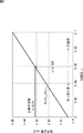
図5は、上述したことを前提に、FeS2とZnSのヘテロ界面を持ったMQW構造の吸収波長を見積もった結果を示す図である。横軸がZnS層の厚みLw(nm)を表し、縦軸が吸収波長λ(nm)を表している。 FIG. 5 is a diagram showing a result of estimating an absorption wavelength of an MQW structure having a hetero interface of FeS 2 and ZnS on the assumption of the above. The horizontal axis represents the thickness Lw (nm) of the ZnS layer, and the vertical axis represents the absorption wavelength λ (nm).
図5に示されるように、ZnS層の厚みを変化させることで、1.5乃至3.7μmまでの吸収波長を変化させることができる。すなわち、このことは、近赤外乃至中赤外領域までの感度を持つことを意味する。 As shown in FIG. 5, the absorption wavelength from 1.5 to 3.7 μm can be changed by changing the thickness of the ZnS layer. That is, this means that it has sensitivity from the near infrared region to the mid infrared region.
ただし、波長をより長波長側に設定しておけば、短波長側も吸収することになるが、ZnSを厚くする必要がある。このとき、サブバンドが形成できる範囲に限定される。 However, if the wavelength is set to the longer wavelength side, the shorter wavelength side is also absorbed, but the ZnS needs to be thickened. At this time, it is limited to a range in which a subband can be formed.
<格子整合について>
なお、厳格にいえば、FeS2とZnSのヘテロ界面を持ったMQW構造である光電変換部62とSi基板61とは若干格子不整合が発生している。したがって、Seを添加して格子整合させてもよい。
<About lattice matching>
Strictly speaking, there is a slight lattice mismatch between the
図6は、Se組成比xに対するZnS1-XSeXの格子定数を示す図である。ただし0 ≦X≦ 1。なお、図6は、ZnSeの格子定数がa=5.667Aになることからベガード則(リニアな関係)を用いて求められている。 FIG. 6 is a diagram showing the lattice constant of ZnS 1-X Se X with respect to the Se composition ratio x. However, 0 ≦ X ≦ 1. Note that FIG. 6 is obtained using the Vegard law (linear relationship) because the lattice constant of ZnSe is a = 5.667A.
図6に示されるように、Se組成比x=0.084にすることでZnS1-XSeXの格子定数がSiの格子定数a0=5.431Aに一致することが判る。すなわち、Se組成比x=0.084がZnSSeをSi基板に正確に格子整合させる組成である。なお、図中に示す引っ張り歪と圧縮歪はSi基板の格子整合条件からのずれによるZnS1-XSeXの歪を示す。図6の例においては、格子整合条件のSe組成比X=0.084よりSe組成が低い場合には、ZnS1-XSeX層が引っ張り歪となり、逆にSe組成が高い場合には、ZnS1-XSeX層が圧縮歪となる。 As shown in FIG. 6, it can be seen that the lattice constant of ZnS 1-X Se X coincides with the lattice constant of a 0 = 5.431A of Si by setting the Se composition ratio x = 0.084. That is, the Se composition ratio x = 0.084 is a composition that allows lattice matching of ZnSSe to the Si substrate accurately. The tensile strain and compressive strain shown in the figure indicate the strain of ZnS 1-X Se X due to deviation from the lattice matching condition of the Si substrate. In the example of FIG. 6, when the Se composition is lower than the Se composition ratio X = 0.084 of the lattice matching condition, the ZnS 1-X Se X layer becomes tensile strain, and conversely, when the Se composition is high, ZnS 1 -X Se X layer becomes compressive strain.
図7は、Se組成比xに対するFe(S1-XSeX)2の格子定数を示す図である。ただし0 ≦X≦ 1。なお、図7は、FeSe2の格子定数がa=5.8633Aになることからベガード則(リニアな関係)を用いて求められている。 FIG. 7 is a diagram showing the lattice constant of Fe (S 1-X Se X ) 2 with respect to the Se composition ratio x. However, 0 ≦ X ≦ 1. Note that FIG. 7 is obtained using Vegard's law (linear relationship) because the lattice constant of FeSe 2 is a = 5.8633A.
図7に示されるように、Se組成比x=0.059にすることでFe(S1-XSeX)2の格子定数がSiの格子定数a0=5.431Aに一致することが判る。すなわち、Se組成比x=0.059がFe(S1-XSeX)2をSi基板に正確に格子整合させる組成である。 As shown in FIG. 7, it can be seen that the lattice constant of Fe (S 1-X Se X ) 2 matches the lattice constant a 0 = 5.431A of Si by setting the Se composition ratio x = 0.059. That is, the Se composition ratio x = 0.059 is a composition that allows Fe (S 1-X Se X ) 2 to be lattice-matched accurately with the Si substrate.
以上から、Seを添加することで、Si基板と格子定数を一致させることが可能で、ミスフィット転位が減るとともに高い結晶性の材料が得られる。それとともに光電変換素子やイメージセンサの重要特性である暗電流低減に効果的となる。 From the above, by adding Se, it is possible to match the lattice constant with that of the Si substrate, and misfit dislocations are reduced and a highly crystalline material is obtained. At the same time, it is effective in reducing dark current, which is an important characteristic of photoelectric conversion elements and image sensors.
図8は、N組成比xに対するGaP1-XNXの格子定数を示す図である。ただし0 ≦X≦ 1。なお、図8は、GaNの格子定数がa=4.52Aになることからベガード則(リニアな関係)を用いて求められている。 FIG. 8 is a diagram showing the lattice constant of GaP 1-X N X with respect to the N composition ratio x. However, 0 ≦ X ≦ 1. Note that FIG. 8 is obtained using Vegard's law (linear relationship) because the lattice constant of GaN is a = 4.52A.
図8に示されるように、N組成比x=0.021にすることでGaP1-XNXの格子定数がSiの格子定数a0=5.431Aに一致することが判る。すなわち、N組成比x=0.021がGaP1-XNXをSi基板に正確に格子整合させる組成である。 As shown in FIG. 8, it can be seen that the lattice constant of GaP 1-X N X coincides with the lattice constant a 0 = 5.431A of Si by setting the N composition ratio x = 0.021. That is, the N composition ratio x = 0.021 is a composition that allows GaP 1-X N X to be lattice-matched accurately with the Si substrate.
以上から、Nを添加することで、Si基板と格子定数を一致させることが可能で、ミスフィット転位が減るとともに高い結晶性の材料が得られる。それとともに光電変換素子やイメージセンサの重要特性である暗電流低減に効果的となる。 From the above, it is possible to make the lattice constant coincide with that of the Si substrate by adding N, and misfit dislocations are reduced and a highly crystalline material is obtained. At the same time, it is effective in reducing dark current, which is an important characteristic of photoelectric conversion elements and image sensors.
<格子歪の低減>
ところで、引っ張り歪の層と圧縮歪の層を交互に積層することでMQW全体の歪を無くすことが可能となる。
<Reduction of lattice strain>
By the way, it is possible to eliminate strain of the entire MQW by alternately laminating tensile strain layers and compression strain layers.
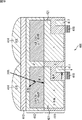
図9は、本技術を適用した固体撮像装置の他の構成例を示す断面図である。 FIG. 9 is a cross-sectional view illustrating another configuration example of the solid-state imaging device to which the present technology is applied.
図9の例においては、固体撮像装置101においては、Si基板111上にTypeIIのヘテロ界面を多数有するMQW構造の光電変換部112が形成されている。
In the example of FIG. 9, in the solid-
光電変換部112においては、FeS2層(またはFe(S1-XSeX)2層)121の引っ張り歪を打ち消すようにZnS1-XSeX層122のSe組成比Xを格子整合条件より増やして圧縮歪とすることで、MQW全体の歪が無くすように構成されている。
In the
このようにすることで、MQW(光電変換部112)を厚く積層しても結晶欠陥の発生が抑えられ、結果として、光電変換素子またはイメージセンサの重要な特性である暗電流の低減となる。 By doing so, the generation of crystal defects is suppressed even when the MQW (photoelectric conversion unit 112) is stacked thick, and as a result, dark current, which is an important characteristic of the photoelectric conversion element or the image sensor, is reduced.
なお、同様にFe(S1-XSeX)2層の圧縮歪を打ち消すようにSe組成またはGa組成を制御してZnS1-XSeXまたはCuIn1-YGaY (S1-XSeX)2を引っ張り歪、またはN組成を制御してGaP1-XNXを引っ張り歪にしても同様な効果が得られる。ただし0 ≦X,Y≦ 1。 Similarly, ZnS 1-X Se X or CuIn 1-Y Ga Y (S 1-X Se) is controlled by controlling the Se or Ga composition so as to cancel the compressive strain of the Fe (S 1-X Se X ) 2 layer. A similar effect can be obtained even if XP 2 is tensile strain or GaP 1-X N X is tensile strain by controlling N composition. However, 0 ≤ X, Y ≤ 1.
以上においては、FeS2層(またはFe(S1-XSeX)2層)とZnS層(またはZnS1-XSeX層)のヘテロ界面のMQW構造について述べた。これに限らず、同様にFeS2層(またはFe(S1-XSeX)2層)とCuInGaS2層や、FeS2層(またはFe(S1-XSeX)2層)とGaP層(またはGaPN層)のヘテロ界面のMQW構造でも同様な効果が得られる。または、FeS2層(またはFe(S1-XSeX)2層)との組合せであれば、途中で積層材料を変えてもよい。たとえばZnS層(またはZnS1-XSeX層)との界面のMQW構造を途中でCuInGaS2層やGaP層(またはGaP1-XNX層)との界面のMQW構造に変えて堆積させてもよい。 In the above, the MQW structure of the heterointerface between the FeS 2 layer (or Fe (S 1-X Se X ) 2 layer) and the ZnS layer (or ZnS 1-X Se X layer) has been described. Not limited to this, similarly FeS 2 layer (or Fe (S 1-X Se X ) 2 layer) and CuInGaS 2 layer, FeS 2 layer (or Fe (S 1-X Se X ) 2 layer) and GaP layer A similar effect can be obtained with an MQW structure at the heterointerface of (or GaPN layer). Alternatively, if it is a combination with FeS 2 layers (or Fe (S 1-X Se X ) 2 layers), the laminated material may be changed in the middle. For example, the MQW structure at the interface with the ZnS layer (or ZnS 1-X Se X layer) is changed to the MQW structure at the interface with the CuInGaS 2 layer or GaP layer (or GaP 1-X N X layer) and deposited. Also good.
また、上述のMQW構造形成のためのエピタキシャル成長法については、その代表的な方法として、例えば、分子線エピタキシー法(MBE:Molecular Beam Epitaxy)、有機金属気相成長法(MOCVD:Metal Organic Chemical Vapor Deposition)、液相エピタキシー法(LPE:Liquid Phase Epitaxy)、レーザーアブレーション法などがある。エピタキシャル成長する方法であれば基本的にいかなる成膜方法であっても良い。 In addition, with respect to the epitaxial growth method for forming the MQW structure described above, as typical methods, for example, molecular beam epitaxy (MBE), metal organic chemical vapor deposition (MOCVD), or MOCVD: Metal Organic Chemical Vapor Deposition ), Liquid phase epitaxy (LPE), and laser ablation. Basically, any film forming method may be used as long as it is an epitaxial growth method.
<傾斜基板による結晶性改善>
なお、Siのような無極性基板の上に極性をもった化合物半導体材料を成長させると、アンチフェーズドメインが発生することがある。これはアニオンとカチオンが逆転する欠陥のことである。この欠陥をOff基板の採用によって低減できる。
<Improvement of crystallinity by inclined substrate>
When a compound semiconductor material having polarity is grown on a nonpolar substrate such as Si, an antiphase domain may be generated. This is a defect in which the anion and cation are reversed. This defect can be reduced by adopting an Off substrate.
図10は、アンチフューズドメインを説明する図である。 FIG. 10 is a diagram illustrating the antifuse domain.
例えば、<011>方向に、オフしたSi(100)基板を用いることで、成長とともにこの欠陥が減少する。図10に示されるように、I族またはII族またはIII族または鉄のようなVIII族のカチオン(プラスイオン性原子)と、VI族やV族のアニオン(マイナスイオン性原子)が規則配列している。ただし、その一部B領域にアンチフェーズドメイン(カチオンとアニオンが逆位相になっている)が存在しているのが判る。 For example, by using an off Si (100) substrate in the <011> direction, this defect decreases with growth. As shown in FIG. 10, group VIII cations (positive ionic atoms) such as group I, group II, group III or iron and group VI or group V anions (negative ionic atoms) are regularly arranged. ing. However, it can be seen that an anti-phase domain (cation and anion are in reverse phase) exists in part B region.
それが、結晶成長とともに、このB領域が三角形状に閉じることでA領域のみとなり、この欠陥が無くなっていることが判る。これは基板に傾斜角度があるためである。なお、ここでは、たとえばI族原子はCu原子、II族原子ではZn、III族原子はGaまたはIn原子、VIII族原子はFe、VI族原子はSまたはSe原子、V族原子はPまたはN原子などである。図10は、結晶を<011>方向に見た断面図で、カチオン列の四角は、紙面垂直方向に並んでいる。また、図10はアニオンから成長開始の場合であるが、カチオンからの成長開始しでも三角形状に閉じた同様な結果となる。なお、これらの場合の基板傾斜角度θ1は、約6degとなる。傾斜角度が大きくなるほどB領域の三角形は小さくなるが、特に3deg以上あれば、B領域が最大でも、図面で倍程度の大きさで収まり、十分な効果が得られることになる。 It can be seen that, as the crystal grows, this B region closes in a triangular shape to become only the A region, and this defect is eliminated. This is because the substrate has an inclination angle. Here, for example, group I atom is Cu atom, group II atom is Zn, group III atom is Ga or In atom, group VIII atom is Fe, group VI atom is S or Se atom, group V atom is P or N Atoms. FIG. 10 is a cross-sectional view of the crystal in the <011> direction, in which the squares of the cation rows are aligned in the direction perpendicular to the paper surface. FIG. 10 shows the case where growth starts from an anion. Even when growth starts from a cation, a similar result is obtained in a triangular shape. In these cases, the substrate inclination angle θ 1 is about 6 deg. As the tilt angle increases, the triangle in the B region becomes smaller. However, if the angle is 3 deg or more, even if the B region is the maximum, the size is about twice that in the drawing, and a sufficient effect can be obtained.
図11は、図10に示した結晶の鳥瞰図である。図10の例の場合、B領域のアンチフェーズドメインが成長とともに三角形状に閉じているが、B領域のアンチフェーズドメインが奥行き方向(<0 -1 1>方向)で連続的に続いており、結果として三角柱を横に倒した形状になっているのが判る。 FIG. 11 is a bird's-eye view of the crystal shown in FIG. In the example of FIG. 10, the antiphase domain of the B region is closed in a triangular shape as it grows, but the antiphase domain of the B region continues continuously in the depth direction (<0 -1 1> direction) As a result, it can be seen that the triangular prism is tilted sideways.
このB領域のアンチフェーズドメインの体積を減らす手段として、さらに望ましくは、図12のように<0 -1 1>方向にも同時に傾斜させることで可能となる。なお、Si基板にとっては<011>方向も<0-11>方向も等価な方向なので、どちらも同じ効果を生むことになる。 As a means for reducing the volume of the anti-phase domain in the region B, it is more preferable to simultaneously incline in the <0-1 1> direction as shown in FIG. For the Si substrate, both the <011> direction and the <0-11> direction are equivalent directions, and both produce the same effect.
たとえば、<0-11>方向にも傾斜角度θ2で傾斜させると、三角形状に閉じる効果が垂直な二方向から同時にあるために、結果として三角錐となり、体積は減ることになる。このとき、両者の傾斜角度が3deg以上でまったく同じ角度で傾斜されれば、方位が合成されて<001>方向の傾斜となり、そのときの合成の傾斜は4deg以上となり、最も効果的な条件を満たすことになる。このときアンチフェーズドメインの体積は1方向のみの傾斜に比べて、2方向で1/3まで減じることになる。ただし、製造的な面から言うと、バラツキを含めて<001>±5deg方向であれば、最も効果的と言える。 For example, when tilting in the <0-11> direction at an inclination angle θ 2 as well, the effect of closing in a triangular shape is simultaneously from two perpendicular directions, resulting in a triangular pyramid and a decrease in volume. At this time, if the inclination angle of both is 3 deg or more and the inclination is exactly the same angle, the azimuth is combined to become the inclination of <001> direction, and the combined inclination at that time is 4 deg or more, which is the most effective condition. Will meet. At this time, the volume of the anti-phase domain is reduced to 1/3 in two directions compared to the inclination in only one direction. However, in terms of manufacturing, it is most effective if the direction is <001> ± 5 deg including variations.
以上の結果から、<011>と<0-11>の傾斜角度が、両方とも3deg以上であれば効果的であるといえる。また両方の傾斜角度が異なる場合でも、やはり効果がある。この場合、傾斜方向は<011>と<0-11>の合成となるので、両者の傾斜角度の比で変化する。方位が<011>と<0-11>の合成で両者の合成の傾斜角度が3deg以上あれば、効果的に両者のアンチフェーズドメインが抑えられることになる。この場合、傾斜角度の比をkとすると、傾斜の方位は< 0 (1-k)/2 1 >となる。ここで傾斜角度の比kは、<011>方向の傾斜角度をθ1, <0-11>方向の傾斜角度をθ2とすると、次の式(3)で定義される。 From the above results, it can be said that it is effective if the inclination angles of <011> and <0-11> are both 3 deg or more. Moreover, even if both inclination angles are different, it is still effective. In this case, since the inclination direction is a combination of <011> and <0-11>, it changes depending on the ratio of the inclination angles of both. If the azimuth is <011> and <0-11> and the combined inclination angle is 3 deg or more, the antiphase domains of both are effectively suppressed. In this case, if the ratio of the tilt angles is k, the tilt direction is <0 (1-k) / 2 1>. Here, the tilt angle ratio k is defined by the following equation (3), where θ 1 is the tilt angle in the <011> direction, and θ 2 is the tilt angle in the <0-11> direction.
![]()
![]()
<電子障壁層>
ところで、逆バイアスを印加した際に、上部電極から光電変換部へ電子が流れてリークすることがある。これは、上部電極の仕事関数と光電変換部表面側の半導体材料の電子親和力との差が小さいために、電解で電子がポテンシャルを超える現象である。
<Electronic barrier layer>
By the way, when a reverse bias is applied, electrons may flow from the upper electrode to the photoelectric conversion unit and leak. This is a phenomenon in which electrons exceed the potential by electrolysis because the difference between the work function of the upper electrode and the electron affinity of the semiconductor material on the surface of the photoelectric conversion portion is small.
これを防ぐために、上部電極とMQW構造の光電変換部との間に電子のポテンシャル障壁となる層を挿入してもよい。 In order to prevent this, a layer serving as an electron potential barrier may be inserted between the upper electrode and the photoelectric conversion portion of the MQW structure.
図13は、上述した障壁層材料候補の材料の特性を示す図である。図13に示されるように、NiOは、電子親和力(eV)が1.5で、バンドギャップ(eV)が~4.0である。Cu2Oは、電子親和力(eV)が~3.4で、バンドギャップ(eV)が~2.1である。ZnRh2O4は、電子親和力(eV)が~2.3で、バンドギャップ(eV)が~2.2である。 FIG. 13 is a diagram illustrating the characteristics of the above-described barrier layer material candidate materials. As shown in FIG. 13, NiO has an electron affinity (eV) of 1.5 and a band gap (eV) of ˜4.0. Cu 2 O has an electron affinity (eV) of ~ 3.4 and a band gap (eV) of ~ 2.1. ZnRh 2 O 4 has an electron affinity (eV) of ~ 2.3 and a band gap (eV) of ~ 2.2.
障壁層材料候補の中の1つとして、NiOは、電子親和力が1.5と小さく、かつ、バンドギャップも4.0eVと広い。したがって、透明電極(例えば、ITOの仕事関数4.7eV)のフェルミレベルに対して、十分にポテンシャル障壁(~3.2eV)となる。 As one of the barrier layer material candidates, NiO has a small electron affinity of 1.5 and a wide band gap of 4.0 eV. Therefore, it becomes a potential barrier (˜3.2 eV) sufficiently against the Fermi level of the transparent electrode (for example, ITO work function 4.7 eV).
<本技術の固定撮像装置の構成例>
図14は、電子障壁層を追加した固体撮像装置の構成例を示す断面図である。
<Configuration example of fixed imaging device of the present technology>
FIG. 14 is a cross-sectional view illustrating a configuration example of a solid-state imaging device to which an electron barrier layer is added.
図14の固体撮像装置201は、Si基板61および光電変換部62を備える点が、図3の固体撮像装置51と共通している。図14の固体撮像装置201は、上部電極(ITO)と光電変換部62との間に、電子障壁層211が追加された点が、図3の固体撮像装置51と異なっている。
The solid-
図14の例においては、透明電極にITO、電子障壁層211として、NiOが用いられており、かつ、-2Vの逆バイアス印加時のバンド構造が示されている。この結果から、逆バイアスを印加しても、NiOからなる電子障壁層211が機能する構造となっているのがわかる。また、図14の例に、トンネル効果を追加して、ベーテのエミッション理論からJ-V特性を見積もった結果を、図15に示す。
In the example of FIG. 14, ITO is used for the transparent electrode, NiO is used as the
図15の例においては、NiOの電子障壁層211なしの場合、NiOの電子障壁層211が5nmの場合、およびNiOの電子障壁層211が10nmの場合のグラフが示されている。このグラフにおいては、横軸がバイアスV(V)を表し、縦軸が電流密度J(A/cm2)を表している。
In the example of FIG. 15, a graph is shown in the case where the NiO
このグラフからNiOの電子障壁層211を10nm以上とすることで、-2Vの電圧印加条件でも電流密度がJ=1×10-11A/cm2以下となっていることがわかる。この値は、通常のシャッタ時間1/30秒で撮影しても、暗電流の蓄積電子数は、数電子以下となり、イメージセンサにとって十分な条件となる。なお、NiOの経時変化を小さくするために、NiOにLiをドープしてもよい。
From this graph, it can be seen that by setting the NiO
次に、電子障壁層211の材料をCu2Oにした場合について述べる。この場合は、透明電極(例えば、ITOの仕事関数4.7eV)のフェルミレベルに対して、十分に障壁(1.3eV)になる。透明電極にITOを、そして、電子障壁層211にCu2Oを用いて、かつ逆バイアス印加時のトンネル効果を入れて、J-V特性を見積もった結果を、図16に示す。
Next, the case where the material of the
図16の例においては、Cu2Oの電子障壁層211なしの場合、Cu2Oの電子障壁層211が5nmの場合、およびCu2Oの電子障壁層211が10nmの場合のグラフが示されている。このグラフにおいては、横軸がバイアスV(V)を表し、縦軸が電流密度J(A/cm2)を表している。
In the example of FIG. 16, when the
このグラフからCu2Oの電子障壁層211を10nm以上とすることで、-2Vの電圧印加条件でも電流密度がJ=1×10-11A/cm2以下となっていることがわかる。この値は、通常のシャッタ時間1/30秒で撮影しても、暗電流の蓄積電子数は、数電子以下となり、イメージセンサにとって十分な条件となる。
From this graph, it can be seen that by setting the
なお、上記説明においては、単純に1種類の材料を電子障壁層211としているが、2種類以上を積層させてもよい。例えば、Cu2OとZnRh2O4を積層して障壁層の役割をさせてもよい。この場合、ZnRh2O4だけでも効果があるが、ZnRh2O4の価電子帯がMQWの伝導帯にエネルギ的に近いため、MQWへのリーク電流が懸念される。したがって、Cu2Oをさらに多層に積層することで、電子の障壁がより効果的になる。
In the above description, one type of material is simply used as the
<正孔障壁層>
逆バイアスを印加した際にSi基板から光電変換部へ正孔が流れてリークすることがある。これは、Si基板の価電子帯上端と光電変換部表面側の半導体材料の価電子帯上端との差が小さいために、起こる現象である。
<Hole barrier layer>
When a reverse bias is applied, holes may flow from the Si substrate to the photoelectric conversion unit and leak. This is a phenomenon that occurs because the difference between the upper end of the valence band of the Si substrate and the upper end of the valence band of the semiconductor material on the surface of the photoelectric conversion portion is small.
これを防ぐために、Si基板とMQW構造の光電変換部の間にZnS(またはZnS1-XSeX層) CuInGaS2層、あるいはGaP層(またはGaP1-XNX層)を10nm以上の厚みで成長することで、その層を正孔障壁層とする。または、MQWの第1層目であるZnS(またはZnS1-XSeX層)、CuInGaS2層、あるいはGaP層(またはGaP1-XNX層)のみを10nm以上の厚みで成長することで、その層を正孔障壁層とする。 To prevent this, a ZnS (or ZnS 1-X Se X layer) CuInGaS 2 layer or GaP layer (or GaP 1-X N X layer) with a thickness of 10 nm or more between the Si substrate and the MQW photoelectric conversion part The layer becomes a hole barrier layer. Alternatively, by growing only the first MQW layer ZnS (or ZnS 1-X Se X layer), CuInGaS 2 layer, or GaP layer (or GaP 1-X N X layer) with a thickness of 10 nm or more. The layer is a hole blocking layer.
<本技術の固定撮像装置の構成例>
図17は、正孔障壁層を追加した固体撮像装置の構成例を示す断面図である。
<Configuration example of fixed imaging device of the present technology>
FIG. 17 is a cross-sectional view illustrating a configuration example of a solid-state imaging device to which a hole blocking layer is added.
図17の固体撮像装置251は、Si基板61、光電変換部62、電子障壁層211を備える点が、図14の固体撮像装置201と共通している。図17の固体撮像装置251は、Si基板61と光電変換部62との間に、正孔障壁層261が追加された点が、図14の固体撮像装置201と異なっている。
The solid-
このように固定撮像装置を構成することで、さらに暗電流が減って、特性改善となる。 By configuring the fixed imaging device in this way, the dark current is further reduced and the characteristics are improved.
以上のように、本技術は、Si基板に格子整合する化合物半導体材料を用いて、TypeIIのヘテロ界面を有するMQW構造を形成することで、実効的にナローギャップ化して、サブバンド間遷移させるものである。本技術は、近赤外乃至中赤外光まで感度を持つ光電子変換素子またはイメージセンサに適用することができる。 As described above, this technology uses a compound semiconductor material lattice-matched to a Si substrate to form an MQW structure with a Type II heterointerface, effectively narrowing the gap and causing intersubband transitions. It is. The present technology can be applied to a photoelectric conversion element or an image sensor having sensitivity from near infrared light to mid infrared light.
本技術は、また、大面積のSi基板に適用できるため、量産化が可能となり、低コストで安価な光電変換素子またはイメージセンサを提供することができる。 Since the present technology can also be applied to a large-area Si substrate, mass production is possible, and a low-cost and inexpensive photoelectric conversion element or image sensor can be provided.
<光電変換素子の構成例>
図18は、本技術の固体撮像装置に含まれる光電変換素子の構成例を示す断面図である。
<Configuration example of photoelectric conversion element>
FIG. 18 is a cross-sectional view illustrating a configuration example of the photoelectric conversion element included in the solid-state imaging device of the present technology.
図18の例においては、光電変換素子301が示されている。光電変換素子301においては、予めイオン注入とアニール処理でSi基板311の一部にn型領域312が設けられている。
In the example of FIG. 18, a
n型領域312上には、1%未満の格子不整合率の絶対値で、かつ厚みが3nmのp型ZnS層321と厚みが3nmのp型FeS2層322が交互に積層されたMQW構造からなる化合物半導体の光電変換部313が3000nmの厚みで形成されている。また、n型領域312上には、光電変換部313からの電子を送るためのAI電極314が形成されている。
On the n-
ここで、Si基板311上の最初の第1層目のZnS層321に関しては、必ずにも3nmと薄くすることはなく、10nm以上の厚みでも信号読み出しを行うことができる。
Here, the first
なお、結晶性を向上させるために、図6および図7を参照して上述したように、FeS2とZnSにSeを添加してFe(S1-XSeX)2とZnS1-XSeXとしてSi基板に格子整合させてもよい。また、図9を参照して上述したように圧縮と引っ張りを交互に入れた方法で歪を緩和してもよい。格子整合条件はFe(S1-XSeX)2の場合、X=0.059でZnS1-XSeXの場合X=0.084である。 In order to improve crystallinity, as described above with reference to FIG. 6 and FIG. 7, Fe (S 1-X Se X ) 2 and ZnS 1-X Se are added by adding Se to FeS 2 and ZnS. X may be lattice matched to the Si substrate. Further, as described above with reference to FIG. 9, the strain may be alleviated by a method in which compression and tension are alternately inserted. The lattice matching conditions are X = 0.059 for Fe (S 1-X Se X ) 2 and X = 0.084 for ZnS 1-X Se X.
また、FeS2(またはFe(S1-XSeX)2)は、CuまたはAsをドーピングすることでp型の導電性を示す。または、ドーピングしなくても化学量論比とくらべてSまたはSeを過剰とすることでp型の導電性を示す。ZnS(またはZnS1-XSeX)に関しては、窒素ドーピングすることでp型になる。このとき特にプラズマドーピングすることでさらにp型になりやすい。 FeS 2 (or Fe (S 1-X Se X ) 2 ) exhibits p-type conductivity by doping with Cu or As. Alternatively, p-type conductivity is exhibited by adding S or Se in excess of the stoichiometric ratio without doping. ZnS (or ZnS 1-X Se X ) becomes p-type by nitrogen doping. At this time, it is more likely to be p-type by plasma doping.
さらに表面側をp+にして、バンド構造的に表面準位から発生する暗電流を下げる検討をしてもよい。 Further, the surface side may be set to p + to reduce the dark current generated from the surface level in the band structure.
例えば、図19に示される固体撮像装置401は、ドーピング制御による画素分離構造、かつ、正孔蓄積のp+層を付加したHAD(HoleAccumulationDiode)構造をなしている。
For example, the solid-
固体撮像装置401においては、Si基板411の一部に、n型領域421が設けられている。Si基板411の上にはMQW光電変換部412が形成されいる。MQW光電変換部412は、n型領域421上に、p型領域431の形成後、画素分離のためのドーピング制御により、一部にp+領域432が形成される。さらに、MQW光電変換部412においては、表面側にp+領域432が形成される。すなわち、固体撮像装置401においては、p+領域432により、p型領域431上に画素を溜めることができるため、画素分離構造が実現されているとともに、HAD構造が実現されて、正孔が誘起されるので、暗電流を下げることが可能となる。
In the solid-
なお、p型領域431は、p型でなくてもよく、i型やn型であってもよい。 Note that the p-type region 431 does not have to be p-type, and may be i-type or n-type.
MQW光電変換部412上には、例えば、透明電極413が形成され、透明電極413上には、OCL(On Chip Lens)414が形成されている。
For example, a
また、Si基板411のp型領域においては、読み出し回路417が形成されており、読み出し回路417付近には、MOSゲート418が形成されている。
Further, a
以上のように構成される固体撮像装置401において、IR光は、図19に示されるように、OCL414、および透明電極413を介して、p型領域431に入射され、p型領域431において、電子と正孔に分離される。正孔は、p+層のMQW光電変換部412側に、さらには透明電極413側に排出され、電子は、n型領域421から、読み出し回路417を経由して、MOSゲート418により外へ読み出される。
In the solid-
このように固体撮像装置をHAD構造とすることで、暗電流を抑えることができる。 Thus, dark current can be suppressed by making a solid-state imaging device into HAD structure.
したがって、図18の光電変換素子301においても、表面側をp+にすることで、バンド構造的に表面準位から発生する暗電流を下げることができる。
Therefore, also in the
なお、図18における光電変換部313のMQWの多層の組み合わせは、FeS2(またはFe(S1-XSeX)2)とZnS(またはZnS1-XSeX)の組み合わせであった。しかしながら、MQWの多層の組合せは、これに限らず、例えば、FeS2またはFe(S1-XSeX)2とCuIn1-YGaYS2 または CuIn1-YGaY (S1-XSeX)2の組合せでもよいし、FeS2(またはFe(S1-XSeX)2)とGaP(またはGaP1-XNX)の組合せでもよい。結晶成長はMBE法としているが、特にMBE法に限らず、MOCVD法でも、レーザーアブレーション法でも他の方法でもよい。 Note that the MQW multilayer combination of the photoelectric conversion unit 313 in FIG. 18 is a combination of FeS 2 (or Fe (S 1-X Se X ) 2 ) and ZnS (or ZnS 1-X Se X ). However, the combination of MQW multilayers is not limited to this. For example, FeS 2 or Fe (S 1-X Se X ) 2 and CuIn 1-Y Ga Y S 2 or CuIn 1-Y Ga Y (S 1-X A combination of Se X ) 2 may be used, or a combination of FeS 2 (or Fe (S 1-X Se X ) 2 ) and GaP (or GaP 1-X N X ). The crystal growth is performed by the MBE method, but not limited to the MBE method, and the MOCVD method, the laser ablation method, or other methods may be used.
さらに、光電変換部313上には、透過性を有する電子障壁層315が10nmの厚みでスパッタ等の蒸着法で成膜される。電子障壁層315は、例えば、NiOを用いて形成されている。さらにその上に、透光性を有する電極層316が100nmの厚みで同じくスパッタ等の蒸着法で形成されている。この電極層316は、例えばインジウムスズオキサイド(ITO)等の透明電極材料で形成される。この電子障壁層315が存在するために逆バイアス印加時でも電極層316から光電変換部313のMQW側への電子の移動が防がれて、リーク電流が抑えられる。また光照射によって光電変換部313のMQWで生成された正孔は、電極層316側に排出可能である。
Further, a transparent
なお、ここでは電子障壁層315としてNiOを用いているがCu2OやZnRh2O4でも、あるいは、これらを組み合わせた多層構造でも同様な効果が得られる。さらにその上にリソグラフィ技術でマスクを形成した後に光電変換部313と電子障壁層315と電極層316をドライ加工する。さらにマスクを除去後に、この電極層316の上に一部AI電極317を蒸着した後に、保護膜として周囲にSi3N4からなるパッシベーション層318を設ける。この光電変換素子301の2つの電極間に逆バイアスを印加することで、波長≦〜2.5μmまでの長波長のIR光を検知することが可能となる。
Although NiO is used as the
<2.第2の実施例>
<固体撮像装置の第1の構成例>
図20は、本技術を適用した固体撮像装置の構成例を示す断面図である。図20においては、溝による画素分離構造を有する場合の例が示されている。
<2. Second Embodiment>
<First Configuration Example of Solid-State Imaging Device>
FIG. 20 is a cross-sectional view illustrating a configuration example of a solid-state imaging device to which the present technology is applied. FIG. 20 shows an example in the case of having a pixel separation structure with grooves.
固体撮像装置451において、Si基板461側のドーピング制御による画素分離のプロセスの1つには、イオン注入や熱拡散でドーパントを選択的に入れてアニールすることにより、p型とn型の濃度制御を行うことが可能である。
In the solid-
電極やトランジスタ等のCISプロセスを行うことで所望の構造を予めn型のSi基板461の回路側に通常のCISのイオン注入プロセス等でMOSゲート、FDやPDやリセット部などの回路部462が形成される。このSi基板461を支持基板に貼り合せる。Si基板461のn型領域461aの上に1%未満の格子不整合率の絶対値で、かつ厚みが3nmのp型FeS2層と厚みが3nmのp型ZnS層が交互に積層されたMQW構造からなる化合物半導体の光電変換部463が3000nmの厚みで形成される。ここでSi基板461上の最初の第1層目のZnSに関しては、必ずしも3nmと薄くする必要はなく、10nm以上の厚みでも信号読み出しとしてもよい。
A
なお、ここで結晶性を向上させるためにFeS2とZnSにSeを添加してFe(S1-XSeX)2とZnS1-XSeXとしてSi基板461に格子整合させてもよいし、図9を参照して上述したように、圧縮と引っ張りを交互に入れた方法で歪を緩和してもよい。格子整合条件はFe(S1-XSeX)2の場合、X=0.059でZnS1-XSeXの場合X=0.084である。
Here, in order to improve the crystallinity, Se may be added to FeS 2 and ZnS to lattice match with the
また、ここでFeS2(またはFe(S1-XSeX)2)は、CuまたはAsをドーピングすることでp型の導電性を示す。または、ドーピングしなくても化学量論比とくらべてSまたはSeを過剰とすることでp型の導電性を示す。ZnS(またはZnS1-XSeX)に関しては、窒素ドーピングすることでp型になる。このとき特にプラズマドーピングすることでさらにp型になりやすい。なお、FeS2(またはFe(S1-XSeX)2)およびZnS(またはZnS1-XSeX)は、どちらか一方がp型になると、その層においてフェルミレベルが価電子帯に近づき、かつ、隣の層もつられて同時にフェルミレベルが価電子帯に近づくために、全体的にp型になるので、p型となるのは、どちらか一方だけでもよい。さらに、図19を参照して上述したように、表面側をp+にして、バンド構造的に表面準位から発生する暗電流を下げる検討をしてもよい。 Here, FeS 2 (or Fe (S 1-X Se X ) 2 ) exhibits p-type conductivity by doping with Cu or As. Alternatively, p-type conductivity is exhibited by adding S or Se in excess of the stoichiometric ratio without doping. ZnS (or ZnS 1-X Se X ) becomes p-type by nitrogen doping. At this time, it becomes easier to become p-type by plasma doping. Note that when either FeS 2 (or Fe (S 1-X Se X ) 2 ) or ZnS (or ZnS 1-X Se X ) becomes p-type, the Fermi level approaches the valence band in that layer. In addition, since the Fermi level approaches the valence band at the same time as it is entangled with the adjacent layer, it becomes p-type as a whole, so only one of them may be p-type. Further, as described above with reference to FIG. 19, the surface side may be set to p + to reduce the dark current generated from the surface level in the band structure.
ここでの光電変換部463におけるMQWの多層の組合せはFeS2またはFe(S1-XSeX)2とZnSまたはZnS1-XSeXの組み合わせが記載されているが、FeS2またはFe(S1-XSeX)2とCuIn1-YGaYS2 または CuIn1-YGaY (S1-XSeX)2の組合せでもよいし、FeS2またはFe(S1-XSeX)2とGaPまたはGaP1-XNXの組合せでもよい。結晶成長はMBE法としているが、特にMBE法に限らず、MOCVD法でも、レーザーアブレーション法でも他の方法でもよい。
The MQW multilayer combination in the
固体撮像装置451においては、光電変換部463が形成された後に、電子障壁層であるNiO層464がスパッタ蒸着によって光電変換部463上に成膜される。ここで電子ガンやレーザーアブレーションによる真空蒸着でもNiO層464の成膜は可能である。また電子障壁層としては、NiO以外でもCu2OやZnRh2O4でも同様な方法で成膜可能である。
In the solid-
さらに透明電極であるITO465をスパッタ蒸着した後にリソグラフィ技術で選択的に画素ごとにレジストを付けて、RIE加工でITO465とNiO層464と光電変換部463が部分的に除去される。さらにレジストを除去した後に、SiO2層466をCVD法で成膜して溝に埋め込まれる。さらにCMP (Chemical Mechanical Polishing)研磨で最表面のSiO2層466が取り除かれ、ITO467がスパッタ蒸着された後に、パッシベーション膜468としてSi3N4がその上にCVDで成膜する。
Further,
なお、ここでは、パッシベーション膜468としてSi3N4を使っているが、(Si3N4)X(SiO2)1-XでもSiO2でも同様に効果がある。さらに表面を平坦にするために高分子材料をスピンコートで塗布し、高分子層469が形成された後に、通常のOCLプロセスで各画素上にOCL470が形成される。なお、上部のITO467は共通電極となる。これにより波長≦〜2.5μmまでの長波長のIR光を検知できるイメージセンサとなる。
Here, Si 3 N 4 is used as the
<3.第3の実施例>
<固体撮像装置の第2の構成例>
図21は、本技術を適用した固体撮像装置の構成例を示す断面図である。図21においては、P+による画素分離構造を有する場合の例が示されている。
<3. Third Example>
<Second Configuration Example of Solid-State Imaging Device>
FIG. 21 is a cross-sectional view illustrating a configuration example of a solid-state imaging device to which the present technology is applied. FIG. 21 shows an example in the case of having a pixel separation structure by P +.
図21の固体撮像装置501は、Si基板461、n型領域461a、回路部462、光電変換部463、NiO層464、ITO467、パッシベーション膜468、高分子層469、OCL469を備える点が、図20の固体撮像装置451と共通している。
The solid-
図21の固体撮像装置501は、SiO2層466での画素分離が、p+層511での画素分離に入れ替わった点、および、ITO465が除かれた点が、図20の固体撮像装置451と異なっている。
The solid-
すなわち、固体撮像装置501においては、光電変換部463が形成された後、リソグラフィ技術で選択的に画素毎にレジストのマスクを付けて、ドーパントとなるAs+またはCu+がイオン注入される。さらに、400℃以上の熱処理を行い、ドーパントを活性化することで、P+層511が形成される。あるいは、p濃度の濃くし、その結果p濃度の濃い層511が形成される。
That is, in the solid-
なお、ここでは主に光電変換部(MQW)463のFeS2またはFe(S1-XSeX)2層がp+層511となり、ZnS(またはZnS1-XSeX)のp濃度が変化しなくても、光電変換部(MQW)463全体でp+となる。さらにその上に電子障壁層であるNiO層464がスパッタ蒸着によって光電変換部(MQW)463上に成膜される。ここで電子ガンやレーザーアブレーションによる真空蒸着でもNiOの成膜は可能である。またNiO以外でもCu2OやZnRh2O4でも同様な方法で成膜可能である。
Here, the FeS 2 or Fe (S 1-X Se X ) 2 layer of the photoelectric conversion part (MQW) 463 mainly becomes the p +
さらに、ITO467がスパッタ蒸着された後に、パッシベーション膜468としてSi3N4がその上にCVDで成膜される。なお、ここではSi3N4を使っているが、(Si3N4)X(SiO2)1-XでもSiO2でも同様に効果がある。さらに表面を平坦にするために高分子材料をスピンコートで塗布し、高分子層469が形成された後に、通常のOCLプロセスで各画素上にOCL470を形成させる。なお、ITO467は共通電極となる。これにより、少なくとも波長≦〜2.5μmまでの長波長のIR光を検知できるイメージセンサとなる。
Further, after
<4.第4の実施例>
<固体撮像装置の第3の構成例>
図22は、本技術を適用した固体撮像装置の構成例を示す断面図である。図22においては、イオン注入の高抵抗化による画素分離構造を有する場合の例が示されている。
<4. Fourth embodiment>
<Third Configuration Example of Solid-State Imaging Device>
FIG. 22 is a cross-sectional view illustrating a configuration example of a solid-state imaging device to which the present technology is applied. FIG. 22 shows an example in the case of having a pixel separation structure by increasing the resistance of ion implantation.
図22の固体撮像装置551は、Si基板461、n型領域461a、回路部462、光電変換部463、NiO層464、ITO467、パッシベーション膜468、高分子層469、OCL469を備える点が、図20の固体撮像装置451と共通している。
The solid-
図22の固体撮像装置551は、SiO2層466での画素分離が、高抵抗領域561での画素分離に入れ替わった点、および、ITO465が除かれた点が、図20の固体撮像装置451と異なっている。
The solid-
すなわち、固体撮像装置551においては、光電変換部463が形成された後、リソグラフィ技術で選択的に画素毎にレジストのマスクを付けて、イオン注入によって光電変換部(MQW)463が電気的に高抵抗化となるB+またはH+をイオン注入する。なお、高抵抗化すれば、特にイオン種はなんでもよい。このとき、光電変換部(MQW)463の画素間が高抵抗化され、高抵抗領域561となるため、光電流は画素の中央付近のみを流れるために、結果的に画素分離が可能となる。
That is, in the solid-
さらにその上に電子障壁層であるNiO層464がスパッタ蒸着によって光電変換部(MQW)463上に成膜される。ここで電子ガンやレーザーアブレーションによる真空蒸着でもNiOの成膜は可能である。またNiO以外でもCu2OやZnRh2O4でも同様な方法で成膜可能である。
Furthermore, a
さらに、ITO467がスパッタ蒸着された後に、パッシベーション膜468としてSi3N4がその上にCVDで成膜される。なお、ここではSi3N4を使っているが、(Si3N4)X(SiO2)1-XでもSiO2でも同様に効果がある。さらに表面を平坦にするために高分子材料をスピンコートで塗布し、高分子層469が形成された後に、通常のOCLプロセスで各画素上にOCL470を形成させる。なお、ITO467は共通電極となる。これにより、少なくとも波長≦〜2.5μmまでの長波長のIR光を検知できるイメージセンサとなる。
Further, after
<5.第5の実施例>
<固体撮像装置の第4の構成例>
図23は、本技術を適用した固体撮像装置の構成例を示す断面図である。図23においては、選択成長制御によるp+画素分離構造を有する場合の例が示されている。
<5. Fifth embodiment>
<Fourth Configuration Example of Solid-State Imaging Device>
FIG. 23 is a cross-sectional view illustrating a configuration example of a solid-state imaging device to which the present technology is applied. FIG. 23 shows an example in the case of having a p + pixel separation structure by selective growth control.
図23の固体撮像装置601は、Si基板461、n型領域461a、回路部462、光電変換部463、NiO層464、ITO467、パッシベーション膜468、無機材料膜611およびp+領域612での画素分離に入れ替わった点、および、ITO465が除かれた点が、図20の固体撮像装置451と異なっている。
The solid-
すなわち、固体撮像装置601においては、Si基板461を支持基板に貼り合せた後、さらに、画素と画素の間の上に、部分的にSiO2などの選択成長のマスクとなる無機材料膜611がリソグラフィ技術とドライエッチング技術で形成される。その後、図20の固体撮像装置451と同様に、Si基板461のn型領域461aの上に1%未満の格子不整合率の絶対値で、かつ厚みが3nmのp型FeS2層と厚みが3nmのp型ZnS層が交互に積層されたMQW構造からなる化合物半導体の光電変換部463が3000nmの厚みで形成される。ここでSi基板461上の最初の第1層目のZnSに関しては、必ずしも3nmと薄くする必要はなく、10nm以上の厚みでも信号読み出しとしてもよい。
That is, in the solid-
なお、ここで結晶性を向上させるためにFeS2とZnSにSeを添加してFe(S1-XSeX)2とZnS1-XSeXとしてSi基板461に格子整合させてもよいし、図9を参照して上述したように、圧縮と引っ張りを交互に入れた方法で歪を緩和してもよい。格子整合条件はFe(S1-XSeX)2の場合、X=0.059でZnS1-XSeXの場合X=0.084である。
Here, in order to improve the crystallinity, Se may be added to FeS 2 and ZnS to lattice match with the
また、ここでFeS2(またはFe(S1-XSeX)2)は、CuまたはAsをドーピングすることでp型の導電性を示す。または、ドーピングしなくても化学量論比とくらべてSまたはSeを過剰とすることでp型の導電性を示す。ZnS(またはZnS1-XSeX)に関しては、窒素ドーピングすることでp型になる。このとき特にプラズマドーピングすることでさらにp型になりやすい。なお、FeS2(またはFe(S1-XSeX)2)およびZnS(またはZnS1-XSeX)は、どちらか一方がp型になるとつられて全体的にp型になるので、p型となるのは、どちらか一方だけでもよい。 Here, FeS 2 (or Fe (S 1-X Se X ) 2 ) exhibits p-type conductivity by doping with Cu or As. Alternatively, p-type conductivity is exhibited by adding S or Se in excess of the stoichiometric ratio without doping. ZnS (or ZnS 1-X Se X ) becomes p-type by nitrogen doping. At this time, it becomes easier to become p-type by plasma doping. Since FeS 2 (or Fe (S 1-X Se X ) 2 ) and ZnS (or ZnS 1-X Se X ) are either p-type and become p-type as a whole, p Only one of them can be a mold.
さらに、ラテラテル成長を入れて画素間と光電変換部463の表面にドーパントを増やしてp+にして成長し、これによって、画素分離とバンド構造的に表面準位から発生する電流を下げることが同時にできる。
Further, the lateral growth is performed to increase the dopant between the pixels and on the surface of the
選択成長かラテラテル成長の制御は、成長条件を変えることで達成できる。例えば、MDCVDでは、減圧にすると選択成長となり、圧力を上げるとラテラテルにも成長する。 Control of selective growth or lateral growth can be achieved by changing growth conditions. For example, in MDCVD, selective growth occurs when the pressure is reduced, and lateral growth occurs when the pressure is increased.
ここでの光電変換部463におけるMQWの多層の組合せはFeS2またはFe(S1-XSeX)2とZnSまたはZnS1-XSeXの組み合わせが記載されているが、FeS2またはFe(S1-XSeX)2とCuIn1-YGaYS2 または CuIn1-YGaY (S1-XSeX)2の組合せでもよいし、FeS2またはFe(S1-XSeX)2とGaPまたはGaP1-XNXの組合せでもよい。結晶成長はMBE法としているが、特にMBE法に限らず、MOCVD法でも、レーザーアブレーション法でも他の方法でもよい。
The MQW multilayer combination in the
固体撮像装置601においては、光電変換部463が形成された後、次の工程として、電子障壁層であるNiO層464がスパッタ蒸着によって光電変換部463上に成膜される。ここで電子ガンやレーザーアブレーションによる真空蒸着でもNiO層464の成膜は可能である。また電子障壁層としては、NiO以外でもCu2OやZnRh2O4でも同様な方法で成膜可能である。
In the solid-
さらに、ITO467がスパッタ蒸着された後に、パッシベーション膜468としてSi3N4がその上にCVDで成膜される。なお、ここではSi3N4を使っているが、(Si3N4)X(SiO2)1-XでもSiO2でも同様に効果がある。さらに表面を平坦にするために高分子材料をスピンコートで塗布し、高分子層469が形成された後に、通常のOCLプロセスで各画素上にOCL470を形成させる。なお、ITO467は共通電極となる。これにより、少なくとも波長≦〜2.5μmまでの長波長のIR光を検知できるイメージセンサとなる。
Further, after
なお、上記説明においては、波長≦〜2.5μmまでの長波長のIR光を検知できると説明したが、本技術によれば、可視光も検知可能である。 In the above description, it has been described that IR light having a long wavelength up to a wavelength ≦ ˜2.5 μm can be detected. However, according to the present technology, visible light can also be detected.
また、上記説明においては、裏面照射型の固体撮像装置の例を説明したが、本技術は、表面照射型の固体撮像装置にも適用することができる。 In the above description, an example of a back-illuminated solid-state imaging device has been described. However, the present technology can also be applied to a front-illuminated solid-state imaging device.
以上においては、本技術を、CMOS固体撮像装置に適用した構成について説明してきたが、CCD(Charge Coupled Device)固体撮像装置といった固体撮像装置に適用するようにしてもよい。また、本技術は積層型の固体撮像装置に適用することもできる。 In the above, the configuration in which the present technology is applied to the CMOS solid-state imaging device has been described. However, the present technology may be applied to a solid-state imaging device such as a CCD (Charge Coupled Device) solid-state imaging device. Further, the present technology can also be applied to a stacked solid-state imaging device.
また、本技術を、光電変換素子に適用する構成について説明してきたが、本技術は、光電変換素子と同様に光を検知する装置であれば、夜間使用できる監視カメラや車載用カメラ、同じく車載用として追突防止用ディテクタ、水分量の検出できる等で医療や農業応用など、どのような光検知装置にも適用することができる。 In addition, the configuration in which the present technology is applied to the photoelectric conversion element has been described. However, if the present technology is a device that detects light in the same manner as the photoelectric conversion element, the surveillance camera and the in-vehicle camera that can be used at night, and the in-vehicle For example, it can be applied to any photodetection device such as a medical or agricultural application because it can detect the amount of moisture and detect the amount of water.
なお、本技術は、固体撮像装置への適用に限られるものではなく、撮像装置にも適用可能である。ここで、撮像装置とは、デジタルスチルカメラやデジタルビデオカメラ等のカメラシステムや、携帯電話機等の撮像機能を有する電子機器のことをいう。なお、電子機器に搭載されるモジュール状の形態、すなわちカメラモジュールを撮像装置とする場合もある。 In addition, this technique is not restricted to application to a solid-state imaging device, It can apply also to an imaging device. Here, the imaging apparatus refers to a camera system such as a digital still camera or a digital video camera, or an electronic apparatus having an imaging function such as a mobile phone. In some cases, a module-like form mounted on an electronic device, that is, a camera module is used as an imaging device.
<6.第6の実施の形態>
<電子機器の構成例>
ここで、図24を参照して、本技術を適用した電子機器の構成例について説明する。
<6. Sixth Embodiment>
<Configuration example of electronic equipment>
Here, a configuration example of an electronic device to which the present technology is applied will be described with reference to FIG.
図24に示される電子機器800は、固体撮像装置(素子チップ)801、光学レンズ802、シャッタ装置803、駆動回路804、および信号処理回路305を備えている。固体撮像装置801としては、上述した本技術の第1乃至第5の実施の形態のうちのいずれかの固体撮像装置が設けられる。これにより、光電変換素子などの量産化が可能となり、その結果、低コストで安価な電子機器を提供することができる。
An
光学レンズ802は、被写体からの像光(入射光)を固体撮像装置801の撮像面上に結像させる。これにより、固体撮像装置801内に一定期間信号電荷が蓄積される。シャッタ装置803は、固体撮像装置801に対する光照射期間および遮光期間を制御する。
The
駆動回路804は、固体撮像装置801の信号転送動作およびシャッタ装置803のシャッタ動作を制御する駆動信号を供給する。駆動回路804から供給される駆動信号(タイミング信号)により、固体撮像装置801は信号転送を行う。信号処理回路805は、固体撮像装置801から出力された信号に対して各種の信号処理を行う。信号処理が行われた映像信号は、メモリなどの記憶媒体に記憶されたり、モニタに出力される。
The
なお、本明細書において、上述した一連の処理を記述するステップは、記載された順序に沿って時系列的に行われる処理はもちろん、必ずしも時系列的に処理されなくとも、並列的あるいは個別に実行される処理をも含むものである。 In the present specification, the steps describing the series of processes described above are not limited to the processes performed in time series according to the described order, but are not necessarily performed in time series, either in parallel or individually. The process to be executed is also included.
また、本開示における実施の形態は、上述した実施の形態に限定されるものではなく、本開示の要旨を逸脱しない範囲において種々の変更が可能である。 The embodiments in the present disclosure are not limited to the above-described embodiments, and various modifications can be made without departing from the gist of the present disclosure.
また、以上において、1つの装置(または処理部)として説明した構成を分割し、複数の装置(または処理部)として構成するようにしてもよい。逆に、以上において複数の装置(または処理部)として説明した構成をまとめて1つの装置(または処理部)として構成されるようにしてもよい。また、各装置(または各処理部)の構成に上述した以外の構成を付加するようにしてももちろんよい。さらに、システム全体としての構成や動作が実質的に同じであれば、ある装置(または処理部)の構成の一部を他の装置(または他の処理部)の構成に含めるようにしてもよい。つまり、本技術は、上述した実施の形態に限定されるものではなく、本技術の要旨を逸脱しない範囲において種々の変更が可能である。 In addition, in the above description, the configuration described as one device (or processing unit) may be divided and configured as a plurality of devices (or processing units). Conversely, the configurations described above as a plurality of devices (or processing units) may be combined into a single device (or processing unit). Of course, a configuration other than that described above may be added to the configuration of each device (or each processing unit). Furthermore, if the configuration and operation of the entire system are substantially the same, a part of the configuration of a certain device (or processing unit) may be included in the configuration of another device (or other processing unit). . That is, the present technology is not limited to the above-described embodiment, and various modifications can be made without departing from the gist of the present technology.
以上、添付図面を参照しながら本開示の好適な実施形態について詳細に説明したが、開示はかかる例に限定されない。本開示の属する技術の分野における通常の知識を有するのであれば、特許請求の範囲に記載された技術的思想の範疇内において、各種の変更例また修正例に想到し得ることは明らかであり、これらについても、当然に本開示の技術的範囲に属するものと了解される。 The preferred embodiments of the present disclosure have been described in detail above with reference to the accompanying drawings, but the disclosure is not limited to such examples. It is obvious that various changes and modifications can be conceived within the scope of the technical idea described in the claims if the person has ordinary knowledge in the technical field to which the present disclosure belongs, Of course, it is understood that these also belong to the technical scope of the present disclosure.
なお、本技術は以下のような構成も取ることができる。
(1) シリコン基板の上に、不整合率の絶対値1%未満、かつIV族以外の格子整合系化合物半導体を、少なくとも赤外光に感度を持つように組み合わせて用いたMQW(Multi-Quantum Wells)構造を
備える固体撮像装置。
(2) 前記MQW構造は、TypeIIのヘテロ界面を有し、
サブバンド間遷移が形成されるように各層の厚みが設定されている
前記(1)に記載の固体撮像装置。
(3) 前記ヘテロ界面は、FeS2あるいはFe(S1-X1SeX1)2と、ZnSあるいはZnS1-X2SeX2、CuIn1-Y1GaY1S2あるいはCuIn1-Y2GaY2(S1-X3SeX3)2、またはGaPあるいはGaP1-X4NX4とで形成されている
前記(2)に記載の固体撮像装置。
(4) 前記ヘテロ界面は、FeS2またはFe(S1-X1SeX1)2の引っ張り歪を打ち消すように、Se組成を制御してZnS1-X2SeX2あるいはCuIn1-Y2GaY2(S1-X3SeX3)2を圧縮歪、またはN組成を制御してGaP1-X4NX4を圧縮歪にされている
前記(3)に記載の固体撮像装置。
(5) 前記ヘテロ界面は、Fe(S1-X1SeX1)2の圧縮歪を打ち消すように、Se組成またはGa組成を制御してZnS1-X2SeX2あるいはCuIn1-Y2GaY2(S1-X3SeX3)2を引っ張り歪、またはN組成を制御してGaP1-X4NX4を引っ張り歪にされている
前記(3)に記載の固体撮像装置。
(6) 前記MQW構造の表面側に設けられる電子障壁層と、
前記電子障壁層の上に配置される電極と
をさらに備える
前記(1)乃至(5)のいずれかに記載の固体撮像装置。
(7) 前記電子障壁層は、NiO、Cu2O、またはZnRh2O4を用いて形成されている
前記(6)に記載の固体撮像装置。
(8) 前記電子障壁層の厚みは10nm以上である
前記(6)に記載の固体撮像装置。
(9) 前記シリコン基板と前記MQW構造の間に正孔障壁層を形成するか、または前記MQW構造の前記シリコン基板側の第1層だけを厚くすることで正孔障壁層とする
前記(1)乃至(8)のいずれかに記載の固体撮像装置。
(10) 前記正孔障壁層は、ZnS あるいは、ZnS1-X2SeX2 、CuIn1-Y1GaY1S2あるいは CuIn1-Y2GaY2(S1-X3SeX3)2、またはGaP、あるいはGaP1-X4NX4のどれかひとつを含んで、かつその厚みを10nm以上とされる
前記(9)に記載の固体撮像装置。
(11) 前記シリコン基板として、傾斜基板を用いる
前記(1)乃至(10)のいずれかに記載の固体撮像装置。
(12) 前記傾斜基板は、<011>方向、または<011>と<0 -11>の合成の方向に傾斜した基板である
前記(11)に記載の固体撮像装置。
(13) 画素分離された構造を有する
前記(1)乃至(12)のいずれかに記載の固体撮像装置。
(14) 前記画素分離された構造は、光電変換部の画素間の一部をエッチングで溝を形成することでなされる
前記(13)に記載の固体撮像装置。
(15) 前記画素分離された構造は、光電変換部の画素間の一部をp+にすることでなされる
前記(13)に記載の固体撮像装置。
(16) 前記画素分離された構造は、光電変換部の画素間の一部をイオン注入により高抵抗化にすることでなされる
前記(13)に記載の固体撮像装置。
(17) 光電変換部の表面層がp+である
前記(1)乃至(16)のいずれかに記載の固体撮像装置。
(18) シリコン基板の上に、不整合率の絶対値1%未満、かつIV族以外の格子整合系化合物半導体を、少なくとも赤外光に感度を持つように組み合わせて用いたMQW(Multi-Quantum Wells)構造を
備える光検出器。
(19) 前記MQW構造は、TypeIIのヘテロ界面を有し、
サブバンド間遷移が形成されるように各層の厚みが設定されている
前記(18)に記載の光検出器。
(20) シリコン基板の上に、不整合率の絶対値1%未満、かつIV族以外の格子整合系化合物半導体を、少なくとも赤外光に感度を持つように組み合わせて用いたMQW(Multi-Quantum Wells)構造を
備える固体撮像装置と、
入射光を前記固体撮像装置に入射する光学系と、
前記固体撮像装置から出力される出力信号を処理する信号処理回路と
からなる電子機器。
In addition, this technique can also take the following structures.
(1) MQW (Multi-Quantum) using a combination of lattice-matched compound semiconductors with an absolute value of mismatch rate of less than 1% on the silicon substrate and other than group IV so as to have sensitivity to at least infrared light. Solid-state imaging device with Wells structure.
(2) The MQW structure has a Type II heterointerface,
The solid-state imaging device according to (1), wherein the thickness of each layer is set so that transition between subbands is formed.
(3) The hetero interface includes FeS 2 or Fe (S 1-X1 Se X1 ) 2 , ZnS or ZnS 1-X2 Se X2 , CuIn 1-Y1 Ga Y1 S 2 or CuIn 1-Y2 Ga Y2 (S 1 -X3 Se X3 ) 2 , or GaP or GaP 1-X4 N X4 . The solid-state imaging device according to (2).
(4) The hetero interface controls ZnS 1-X2 Se X2 or CuIn 1-Y2 Ga Y2 (S) by controlling the Se composition so as to cancel the tensile strain of FeS 2 or Fe (S 1-X1 Se X1 ) 2. The solid-state imaging device according to (3), wherein 1-X3 Se X3 ) 2 is compressed strain or GaP 1-X4 N X4 is compressed strain by controlling N composition.
(5) The hetero interface controls ZnS 1-X2 Se X2 or CuIn 1-Y2 Ga Y2 (S) by controlling the Se or Ga composition so as to cancel the compressive strain of Fe (S 1-X1 Se X1 ) 2. The solid-state imaging device according to (3), wherein 1-X3 Se X3 ) 2 is tensile strained or N composition is controlled to make GaP 1-X4 N X4 tensile strained.
(6) an electron barrier layer provided on the surface side of the MQW structure;
The solid-state imaging device according to any one of (1) to (5), further including: an electrode disposed on the electron barrier layer.
(7) The solid-state imaging device according to (6), wherein the electron barrier layer is formed using NiO, Cu 2 O, or ZnRh 2 O 4 .
(8) The solid-state imaging device according to (6), wherein the electron barrier layer has a thickness of 10 nm or more.
(9) A hole barrier layer is formed between the silicon substrate and the MQW structure, or only the first layer on the silicon substrate side of the MQW structure is thickened to form a hole barrier layer. ) To (8).
(10) The hole blocking layer is made of ZnS, ZnS 1-X2 Se X2 , CuIn 1-Y1 Ga Y1 S 2 or CuIn 1-Y2 Ga Y2 (S 1-X3 Se X3 ) 2 , GaP, or GaP The solid-state imaging device according to (9), including any one of 1-X4 N X4 and having a thickness of 10 nm or more.
(11) The solid-state imaging device according to any one of (1) to (10), wherein an inclined substrate is used as the silicon substrate.
(12) The solid-state imaging device according to (11), wherein the tilted substrate is a substrate tilted in a <011> direction or a synthesis direction of <011> and <0-11>.
(13) The solid-state imaging device according to any one of (1) to (12), which has a structure in which pixels are separated.
(14) The solid-state imaging device according to (13), wherein the pixel-separated structure is formed by forming a groove by etching a part between pixels of the photoelectric conversion unit.
(15) The solid-state imaging device according to (13), wherein the pixel-separated structure is formed by setting a part between pixels of the photoelectric conversion unit to p +.
(16) The solid-state imaging device according to (13), wherein the pixel-separated structure is formed by increasing a resistance between a part of pixels of the photoelectric conversion unit by ion implantation.
(17) The solid-state imaging device according to any one of (1) to (16), wherein a surface layer of the photoelectric conversion unit is p +.
(18) MQW (Multi-Quantum) using a combination of a lattice-matched compound semiconductor other than the IV group and a sensitivity of at least infrared light on a silicon substrate with an absolute value of mismatch rate of less than 1%. A photodetector with a Wells structure.
(19) The MQW structure has a Type II heterointerface,
The photodetector according to (18), wherein the thickness of each layer is set so that transition between subbands is formed.
(20) MQW (Multi-Quantum) using a combination of lattice-matched compound semiconductors other than Group IV with an absolute value of mismatch rate of less than 1% on a silicon substrate so as to have sensitivity to at least infrared light. A solid-state imaging device having a Wells structure;
An optical system that makes incident light incident on the solid-state imaging device;
An electronic device comprising: a signal processing circuit that processes an output signal output from the solid-state imaging device.
1 固体撮像装置, 2 画素, 11 半導体基板, 51 固体撮像装置, 61 Si基板, 62 光電変換部, 71 FeS2層, 72 ZnS層, 101 固体撮像装置, 111 Si基板, 112 光電変換部, 121 FeS2層, 122ZnS1-XSeX層, 201 固体撮像装置, 211 電子障壁層, 251 固体撮像装置, 261 正孔障壁層, 301 光電変換素子, 311 Si基板, 312 n型領域, 313 光電変換部, 314 AI電極,315 電子障壁層, 316 電極層,317 AI電極, 318 パッシベーション層, 321 FeS2層, 322 ZnS層, 401 固体撮像装置, 411 Si基板, 412 MQW光電変換部, 413 透明電極, 414 OCL, 417 読み出し回路, 418 MOSゲート, 421 n型領域, 431 p型領域, 432 p+領域, , 451 固体撮像装置, 461 Si基板, 461a n型領域, 463 光電変換部, 464 NiO層, 465 ITO, 466 SiO2層, 467 ITO, 468 パッシベーション膜, 469 高分子層, 470 OCL, 501 固体撮像装置, 511 P+層, 551 固体撮像装置, 561 高抵抗領域, 601 固体撮像装置, 611 無機材料膜, 612 p+領域, 800 電子機器, 801 固体撮像素子, 802 光学レンズ, 803 シャッタ装置, 804 駆動回路, 805 信号処理回路 DESCRIPTION OF SYMBOLS 1 Solid-state imaging device, 2 pixels, 11 Semiconductor substrate, 51 Solid-state imaging device, 61 Si substrate, 62 Photoelectric conversion part, 71 FeS 2 layer, 72 ZnS layer, 101 Solid-state imaging device, 111 Si substrate, 112 Photoelectric conversion part, 121 FeS 2 layer, 122ZnS 1-X Se X layer, 201 solid-state imaging device, 211 electron barrier layer, 251 solid-state imaging device, 261 hole barrier layer, 301 photoelectric conversion element, 311 Si substrate, 312 n-type region, 313 photoelectric conversion Part, 314 AI electrode, 315 electron barrier layer, 316 electrode layer, 317 AI electrode, 318 passivation layer, 321 FeS 2 layer, 322 ZnS layer, 401 solid-state imaging device, 411 Si substrate, 412 MQW photoelectric conversion part, 413 transparent electrode , 414 OCL, 417 readout circuit, 418 MOS gate, 421 n-type region, 431 p-type region, 432 p + region,, 451 solid-state imaging Location, 461 Si substrate, 461a n-type region, 463 a photoelectric conversion unit, 464 NiO layer, 465 ITO, 466 SiO 2 layer, 467 ITO, 468 passivation film, 469 a polymer layer, 470 OCL, 501 solid-state imaging device, 511 P + Layer, 551 solid-state imaging device, 561 high resistance region, 601 solid-state imaging device, 611 inorganic material film, 612 p + region, 800 electronic device, 801 solid-state imaging device, 802 optical lens, 803 shutter device, 804 drive circuit, 805 signal processing circuit
Claims (20)
備える固体撮像装置。 MQW (Multi-Quantum Wells) structure using a combination of lattice matching compound semiconductors other than Group IV with a sensitivity of at least infrared light on a silicon substrate. A solid-state imaging device.
サブバンド間遷移が形成されるように各層の厚みが設定されている
請求項1に記載の固体撮像装置。 The MQW structure has a Type II heterointerface,
The solid-state imaging device according to claim 1, wherein the thickness of each layer is set so that transition between subbands is formed.
請求項2に記載の固体撮像装置。 The heterointerface includes FeS 2 or Fe (S 1-X1 Se X1 ) 2 and ZnS or ZnS 1-X2 Se X2 , CuIn 1-Y1 Ga Y1 S 2 or CuIn 1-Y2 Ga Y2 (S 1-X3 Se The solid-state imaging device according to claim 2 , wherein X 3 ) 2 , GaP, or GaP 1-X4 N X4 is formed.
請求項3に記載の固体撮像装置。 The hetero interface is ZnS 1-X2 Se X2 or CuIn 1-Y2 Ga Y2 (S 1-X3 ) by controlling the Se composition so as to cancel the tensile strain of FeS 2 or Fe (S 1-X1 Se X1 ) 2. The solid-state imaging device according to claim 3, wherein Se X3 ) 2 is compressed strain or GaP 1-X4 N X4 is compressed strain by controlling N composition.
請求項3に記載の固体撮像装置。 The hetero interface is ZnS 1-X2 Se X2 or CuIn 1-Y2 Ga Y2 (S 1-X3) by controlling the Se composition or Ga composition so as to cancel the compressive strain of Fe (S 1-X1 Se X1 ) 2. The solid-state imaging device according to claim 3, wherein Se X3 ) 2 is subjected to tensile strain or N composition is controlled to cause GaP 1-X4 N X4 to be tensile strain.
前記電子障壁層の上に配置される電極と
をさらに備える請求項1に記載の固体撮像装置。 An electron barrier layer provided on the surface side of the MQW structure;
The solid-state imaging device according to claim 1, further comprising: an electrode disposed on the electron barrier layer.
請求項6に記載の固体撮像装置。 The solid-state imaging device according to claim 6, wherein the electron barrier layer is formed using NiO, Cu 2 O, or ZnRh 2 O 4 .
請求項6に記載の固体撮像素装置。 The solid-state imaging device according to claim 6, wherein the electron barrier layer has a thickness of 10 nm or more.
請求項1に記載の固体撮像装置。 The hole blocking layer is formed between the silicon substrate and the MQW structure, or the hole blocking layer is formed by thickening only the first layer on the silicon substrate side of the MQW structure. Solid-state imaging device.
請求項9に記載の固体撮像装置。 The hole blocking layer is made of ZnS or ZnS 1-X2 Se X2 , CuIn 1-Y1 Ga Y1 S 2 or CuIn 1-Y2 Ga Y2 (S 1-X3 Se X3 ) 2 , GaP, or GaP 1-X4 The solid-state imaging device according to claim 9, comprising any one of N X4 and having a thickness of 10 nm or more.
請求項1に記載の固体撮像装置。 The solid-state imaging device according to claim 1, wherein an inclined substrate is used as the silicon substrate.
請求項11に記載の固体撮像装置。 The solid-state imaging device according to claim 11, wherein the inclined substrate is a substrate inclined in a <011> direction or a direction in which <011> and <0-11> are combined.
請求項1に記載の固体撮像装置。 The solid-state imaging device according to claim 1, having a structure in which pixels are separated.
請求項13に記載の固体撮像装置。 The solid-state imaging device according to claim 13, wherein the pixel-separated structure is formed by forming a groove by etching a part between pixels of the photoelectric conversion unit.
請求項13に記載の固体撮像装置。 The solid-state imaging device according to claim 13, wherein the pixel-separated structure is formed by setting a part between pixels of the photoelectric conversion unit to p +.
請求項13に記載の固体撮像装置。 The solid-state imaging device according to claim 13, wherein the pixel-separated structure is achieved by increasing a resistance between pixels of a photoelectric conversion unit by ion implantation.
請求項1に記載の固体撮像装置。 The solid-state imaging device according to claim 1, wherein a surface layer of the photoelectric conversion unit is p +.
備える光検出器。 MQW (Multi-Quantum Wells) structure using a combination of lattice matching compound semiconductors other than Group IV with a sensitivity of at least infrared light on a silicon substrate. A photodetector.
サブバンド間遷移が形成されるように各層の厚みが設定されている
請求項18に記載の光検出器。 The MQW structure has a Type II heterointerface,
The photodetector according to claim 18, wherein the thickness of each layer is set so that a transition between subbands is formed.
備える固体撮像装置と、
入射光を前記固体撮像装置に入射する光学系と、
前記固体撮像装置から出力される出力信号を処理する信号処理回路と
からなる電子機器。 MQW (Multi-Quantum Wells) structure using a combination of lattice matching compound semiconductors other than Group IV with a sensitivity of at least infrared light on a silicon substrate. A solid-state imaging device comprising:
An optical system that makes incident light incident on the solid-state imaging device;
An electronic device comprising: a signal processing circuit that processes an output signal output from the solid-state imaging device.
Priority Applications (3)
| Application Number | Priority Date | Filing Date | Title |
|---|---|---|---|
| JP2013262101A JP2015119067A (en) | 2013-12-19 | 2013-12-19 | Solid-state image pickup device, photodetector and electronic device |
| CN201410768979.7A CN104733483B (en) | 2013-12-19 | 2014-12-12 | Solid-state imaging device, photodetection device, and electronic equipment |
| US14/569,248 US9287314B2 (en) | 2013-12-19 | 2014-12-12 | Solid-state imaging device, light detecting device, and electronic apparatus |
Applications Claiming Priority (1)
| Application Number | Priority Date | Filing Date | Title |
|---|---|---|---|
| JP2013262101A JP2015119067A (en) | 2013-12-19 | 2013-12-19 | Solid-state image pickup device, photodetector and electronic device |
Publications (1)
| Publication Number | Publication Date |
|---|---|
| JP2015119067A true JP2015119067A (en) | 2015-06-25 |
Family
ID=53401014
Family Applications (1)
| Application Number | Title | Priority Date | Filing Date |
|---|---|---|---|
| JP2013262101A Pending JP2015119067A (en) | 2013-12-19 | 2013-12-19 | Solid-state image pickup device, photodetector and electronic device |
Country Status (3)
| Country | Link |
|---|---|
| US (1) | US9287314B2 (en) |
| JP (1) | JP2015119067A (en) |
| CN (1) | CN104733483B (en) |
Cited By (1)
| Publication number | Priority date | Publication date | Assignee | Title |
|---|---|---|---|---|
| WO2017104486A1 (en) | 2015-12-15 | 2017-06-22 | Sony Corporation | Image sensor, image capturing system, and production method of image sensor |
Families Citing this family (9)
| Publication number | Priority date | Publication date | Assignee | Title |
|---|---|---|---|---|
| AU2015374335B2 (en) | 2014-12-23 | 2018-03-29 | Apple Inc. | Optical inspection system and method including accounting for variations of optical path length within a sample |
| WO2016185914A1 (en) * | 2015-05-19 | 2016-11-24 | ソニーセミコンダクタソリューションズ株式会社 | Semiconductor device, solid-state imaging device, electronic device, and method for manufacturing semiconductor device |
| CN108449957B (en) | 2015-09-01 | 2021-03-09 | 苹果公司 | Reference switch architecture for non-contact sensing of a substance |
| CN109073460B (en) | 2016-04-21 | 2022-08-23 | 苹果公司 | Optical system for reference switching |
| EP3688446A2 (en) | 2017-09-29 | 2020-08-05 | Apple Inc. | Resolve path optical sampling architectures |
| CN114545550B (en) * | 2018-02-13 | 2024-05-28 | 苹果公司 | Integrated photonic device with integrated edge outcoupler |
| US11500154B1 (en) | 2019-10-18 | 2022-11-15 | Apple Inc. | Asymmetric optical power splitting system and method |
| EP4176304A1 (en) | 2020-09-09 | 2023-05-10 | Apple Inc. | Optical system for noise mitigation |
| CN113363341A (en) * | 2021-06-24 | 2021-09-07 | 湖南汇思光电科技有限公司 | PIN type InGaAsSb detector and preparation method thereof |
Family Cites Families (9)
| Publication number | Priority date | Publication date | Assignee | Title |
|---|---|---|---|---|
| JPH04130687A (en) * | 1990-09-21 | 1992-05-01 | Toshiba Corp | Manufacture of semiconductor device and manufacture of semiconductor laser |
| US5313073A (en) * | 1992-08-06 | 1994-05-17 | University Of Southern California | Light detector using intersub-valence band transitions with strained barriers |
| US6642537B1 (en) * | 1996-08-27 | 2003-11-04 | California Institute Of Technology | Dual band QWIP focal plane array |
| JPH10199813A (en) * | 1997-01-07 | 1998-07-31 | Mitsubishi Electric Corp | Semiconductor device manufacturing method and semiconductor device |
| WO2002047169A1 (en) * | 2000-12-01 | 2002-06-13 | California Institute Of Technology | Multi-quantum-well infrared sensor array in spatially separated multi-band configuration |
| JP5531744B2 (en) | 2010-04-13 | 2014-06-25 | 住友電気工業株式会社 | Semiconductor wafer, light receiving element, light receiving element array, hybrid detection device, optical sensor device, and method for manufacturing semiconductor wafer |
| JP5132739B2 (en) * | 2010-09-06 | 2013-01-30 | 株式会社東芝 | Semiconductor element |
| CN103180973A (en) * | 2010-11-02 | 2013-06-26 | 皇家飞利浦电子股份有限公司 | Iii-nitride light emitting device |
| US9425249B2 (en) * | 2010-12-01 | 2016-08-23 | Alliance For Sustainable Energy, Llc | Coincident site lattice-matched growth of semiconductors on substrates using compliant buffer layers |
-
2013
- 2013-12-19 JP JP2013262101A patent/JP2015119067A/en active Pending
-
2014
- 2014-12-12 CN CN201410768979.7A patent/CN104733483B/en not_active Expired - Fee Related
- 2014-12-12 US US14/569,248 patent/US9287314B2/en active Active
Cited By (1)
| Publication number | Priority date | Publication date | Assignee | Title |
|---|---|---|---|---|
| WO2017104486A1 (en) | 2015-12-15 | 2017-06-22 | Sony Corporation | Image sensor, image capturing system, and production method of image sensor |
Also Published As
| Publication number | Publication date |
|---|---|
| US9287314B2 (en) | 2016-03-15 |
| US20150179845A1 (en) | 2015-06-25 |
| CN104733483B (en) | 2019-08-09 |
| CN104733483A (en) | 2015-06-24 |
Similar Documents
| Publication | Publication Date | Title |
|---|---|---|
| JP2015119067A (en) | Solid-state image pickup device, photodetector and electronic device | |
| JP5509962B2 (en) | Solid-state imaging device, manufacturing method thereof, and electronic apparatus | |
| EP2939267B1 (en) | Solid-state image pickup device and electronic apparatus | |
| CN107615504B (en) | Photoelectric conversion element and solid-state imaging device | |
| JP5609119B2 (en) | Solid-state imaging device, manufacturing method thereof, and imaging device | |
| CN112823420B (en) | Imaging device based on colloidal quantum dots | |
| WO2008093834A9 (en) | Solid-state imaging device and method for manufacturing the same | |
| WO2009125688A1 (en) | Photoelectric conversion device, method for manufacturing the same, and solid state imaging device | |
| JP2017175102A (en) | Photoelectric conversion element, method for manufacturing the same, and imaging apparatus | |
| US8665363B2 (en) | Solid-state image device, method for producing the same, and image pickup apparatus | |
| KR20230124751A (en) | Light detecting element, multilayer light detecting element and light detecting device | |
| US20210288195A1 (en) | Colloidal Quantum Dot (CQD) Photodetectors and Related Devices | |
| TWI618235B (en) | Quantum dot image sensor | |
| JPWO2017126204A1 (en) | Light receiving element, method of manufacturing light receiving element, imaging element and electronic device | |
| Song et al. | Halide perovskite photodiode integrated CMOS imager | |
| JP6260139B2 (en) | Imaging device and imaging apparatus | |
| CN114586182B (en) | Photoelectric conversion element, electronic device, and light-emitting device | |
| JP6540780B2 (en) | Imaging device and imaging device | |
| US20170309684A1 (en) | Photoelectric conversion device and imaging system |