CN109073460B - Optical system for reference switching - Google Patents
Optical system for reference switching Download PDFInfo
- Publication number
- CN109073460B CN109073460B CN201780024955.2A CN201780024955A CN109073460B CN 109073460 B CN109073460 B CN 109073460B CN 201780024955 A CN201780024955 A CN 201780024955A CN 109073460 B CN109073460 B CN 109073460B
- Authority
- CN
- China
- Prior art keywords
- light
- optics
- examples
- optical
- sample
- Prior art date
- Legal status (The legal status is an assumption and is not a legal conclusion. Google has not performed a legal analysis and makes no representation as to the accuracy of the status listed.)
- Active
Links
Images


Classifications
-
- G—PHYSICS
- G01—MEASURING; TESTING
- G01J—MEASUREMENT OF INTENSITY, VELOCITY, SPECTRAL CONTENT, POLARISATION, PHASE OR PULSE CHARACTERISTICS OF INFRARED, VISIBLE OR ULTRAVIOLET LIGHT; COLORIMETRY; RADIATION PYROMETRY
- G01J3/00—Spectrometry; Spectrophotometry; Monochromators; Measuring colours
- G01J3/02—Details
- G01J3/0205—Optical elements not provided otherwise, e.g. optical manifolds, diffusers, windows
- G01J3/0216—Optical elements not provided otherwise, e.g. optical manifolds, diffusers, windows using light concentrators or collectors or condensers
-
- G—PHYSICS
- G01—MEASURING; TESTING
- G01J—MEASUREMENT OF INTENSITY, VELOCITY, SPECTRAL CONTENT, POLARISATION, PHASE OR PULSE CHARACTERISTICS OF INFRARED, VISIBLE OR ULTRAVIOLET LIGHT; COLORIMETRY; RADIATION PYROMETRY
- G01J3/00—Spectrometry; Spectrophotometry; Monochromators; Measuring colours
- G01J3/02—Details
- G01J3/0205—Optical elements not provided otherwise, e.g. optical manifolds, diffusers, windows
- G01J3/0229—Optical elements not provided otherwise, e.g. optical manifolds, diffusers, windows using masks, aperture plates, spatial light modulators or spatial filters, e.g. reflective filters
-
- G—PHYSICS
- G01—MEASURING; TESTING
- G01J—MEASUREMENT OF INTENSITY, VELOCITY, SPECTRAL CONTENT, POLARISATION, PHASE OR PULSE CHARACTERISTICS OF INFRARED, VISIBLE OR ULTRAVIOLET LIGHT; COLORIMETRY; RADIATION PYROMETRY
- G01J3/00—Spectrometry; Spectrophotometry; Monochromators; Measuring colours
- G01J3/02—Details
- G01J3/0256—Compact construction
-
- G—PHYSICS
- G01—MEASURING; TESTING
- G01J—MEASUREMENT OF INTENSITY, VELOCITY, SPECTRAL CONTENT, POLARISATION, PHASE OR PULSE CHARACTERISTICS OF INFRARED, VISIBLE OR ULTRAVIOLET LIGHT; COLORIMETRY; RADIATION PYROMETRY
- G01J3/00—Spectrometry; Spectrophotometry; Monochromators; Measuring colours
- G01J3/02—Details
- G01J3/0294—Multi-channel spectroscopy
-
- G—PHYSICS
- G01—MEASURING; TESTING
- G01J—MEASUREMENT OF INTENSITY, VELOCITY, SPECTRAL CONTENT, POLARISATION, PHASE OR PULSE CHARACTERISTICS OF INFRARED, VISIBLE OR ULTRAVIOLET LIGHT; COLORIMETRY; RADIATION PYROMETRY
- G01J3/00—Spectrometry; Spectrophotometry; Monochromators; Measuring colours
- G01J3/02—Details
- G01J3/10—Arrangements of light sources specially adapted for spectrometry or colorimetry
- G01J3/108—Arrangements of light sources specially adapted for spectrometry or colorimetry for measurement in the infrared range
-
- G—PHYSICS
- G01—MEASURING; TESTING
- G01J—MEASUREMENT OF INTENSITY, VELOCITY, SPECTRAL CONTENT, POLARISATION, PHASE OR PULSE CHARACTERISTICS OF INFRARED, VISIBLE OR ULTRAVIOLET LIGHT; COLORIMETRY; RADIATION PYROMETRY
- G01J3/00—Spectrometry; Spectrophotometry; Monochromators; Measuring colours
- G01J3/28—Investigating the spectrum
- G01J3/30—Measuring the intensity of spectral lines directly on the spectrum itself
- G01J3/36—Investigating two or more bands of a spectrum by separate detectors
-
- G—PHYSICS
- G01—MEASURING; TESTING
- G01J—MEASUREMENT OF INTENSITY, VELOCITY, SPECTRAL CONTENT, POLARISATION, PHASE OR PULSE CHARACTERISTICS OF INFRARED, VISIBLE OR ULTRAVIOLET LIGHT; COLORIMETRY; RADIATION PYROMETRY
- G01J3/00—Spectrometry; Spectrophotometry; Monochromators; Measuring colours
- G01J3/28—Investigating the spectrum
- G01J3/42—Absorption spectrometry; Double beam spectrometry; Flicker spectrometry; Reflection spectrometry
-
- G—PHYSICS
- G01—MEASURING; TESTING
- G01N—INVESTIGATING OR ANALYSING MATERIALS BY DETERMINING THEIR CHEMICAL OR PHYSICAL PROPERTIES
- G01N21/00—Investigating or analysing materials by the use of optical means, i.e. using sub-millimetre waves, infrared, visible or ultraviolet light
- G01N21/17—Systems in which incident light is modified in accordance with the properties of the material investigated
- G01N21/25—Colour; Spectral properties, i.e. comparison of effect of material on the light at two or more different wavelengths or wavelength bands
-
- G—PHYSICS
- G01—MEASURING; TESTING
- G01N—INVESTIGATING OR ANALYSING MATERIALS BY DETERMINING THEIR CHEMICAL OR PHYSICAL PROPERTIES
- G01N21/00—Investigating or analysing materials by the use of optical means, i.e. using sub-millimetre waves, infrared, visible or ultraviolet light
- G01N21/17—Systems in which incident light is modified in accordance with the properties of the material investigated
- G01N21/47—Scattering, i.e. diffuse reflection
- G01N21/49—Scattering, i.e. diffuse reflection within a body or fluid
-
- G—PHYSICS
- G01—MEASURING; TESTING
- G01N—INVESTIGATING OR ANALYSING MATERIALS BY DETERMINING THEIR CHEMICAL OR PHYSICAL PROPERTIES
- G01N21/00—Investigating or analysing materials by the use of optical means, i.e. using sub-millimetre waves, infrared, visible or ultraviolet light
- G01N21/17—Systems in which incident light is modified in accordance with the properties of the material investigated
- G01N21/47—Scattering, i.e. diffuse reflection
- G01N2021/4704—Angular selective
- G01N2021/4711—Multiangle measurement
Landscapes
- Physics & Mathematics (AREA)
- Spectroscopy & Molecular Physics (AREA)
- General Physics & Mathematics (AREA)
- Health & Medical Sciences (AREA)
- Life Sciences & Earth Sciences (AREA)
- Chemical & Material Sciences (AREA)
- Analytical Chemistry (AREA)
- Biochemistry (AREA)
- General Health & Medical Sciences (AREA)
- Immunology (AREA)
- Pathology (AREA)
- Investigating Or Analysing Materials By Optical Means (AREA)
- Optical Measuring Cells (AREA)
- Spectrometry And Color Measurement (AREA)
Abstract
本发明公开了用于确定样本的一个或多个属性的系统和方法。所公开的系统和方法可能够沿多个位置进行测量,并且可将样本内的多个光学路径重新成像并解析。所述系统可配置有适用于紧凑型系统的一层或两层光学器件。可以简化所述光学器件以减少经涂覆的光学表面的数量和复杂性、标准具效应、制造公差叠加问题,以及基于干涉的光谱误差。所述光学器件的大小、数量和位置可在整个所述样本上和所述样本内的各个位置处实现多个同时或非同时测量。此外,所述系统可配置有位于所述样本和所述光学器件之间的光学间隔件窗口,并且本发明公开了考虑由于包含所述光学间隔件窗口而导致的光学路径变化的方法。

The present invention discloses systems and methods for determining one or more properties of a sample. The disclosed systems and methods may be capable of taking measurements along multiple locations, and may re-image and resolve multiple optical paths within the sample. The system can be configured with one or two layers of optics suitable for compact systems. The optics can be simplified to reduce the number and complexity of coated optical surfaces, etalon effects, manufacturing tolerance stackup issues, and interference-based spectral errors. The optics are sized, numbered and positioned to enable multiple simultaneous or non-simultaneous measurements across the sample and at various locations within the sample. Additionally, the system may be configured with an optical spacer window between the sample and the optical device, and the present invention discloses methods of accounting for optical path changes due to the inclusion of the optical spacer window.
Description
相关申请的交叉引用CROSS-REFERENCE TO RELATED APPLICATIONS
本专利申请要求于2016年4月21日提交的美国临时专利申请62/325,908的优先权,该美国临时专利申请全文以引用方式并入本文。This patent application claims priority to US Provisional Patent Application 62/325,908, filed April 21, 2016, which is incorporated herein by reference in its entirety.
技术领域technical field
本发明整体涉及能够检测样本中的一种或多种物质的参考切换架构,更具体地讲,能够对样本中的一个或多个光学路径重新成像。The present invention generally relates to a reference switching architecture capable of detecting one or more species in a sample, and more particularly, capable of re-imaging one or more optical paths in a sample.
背景技术Background technique
吸收光谱学是一种分析技术,可用于确定样本的一种或多种属性。用于吸收光谱学的常规系统和方法可包括将光发射到样本中。由于光透射穿过样本,光能量的一部分以一个或多个波长被吸收。此吸收可引起离开样本的光的属性的变化。可以将离开样本的光的属性与离开参考对象的光的属性进行比较,并且可基于该比较来确定样本的一种或多种属性。Absorption spectroscopy is an analytical technique that can be used to determine one or more properties of a sample. Conventional systems and methods for absorption spectroscopy can include emitting light into a sample. As light is transmitted through the sample, a portion of the light energy is absorbed at one or more wavelengths. This absorption can cause a change in the properties of the light leaving the sample. Properties of light exiting the sample can be compared to properties of light exiting a reference object, and one or more properties of the sample can be determined based on the comparison.
可使用来自一个或多个检测器像素的测量来确定离开样本的光的属性。沿样本内多个位置的测量可用于准确确定样本中的一种或多种属性。这些多个位置可位于样本中的不同位置,这可导致具有不同路径长度、入射角和出射位置的光学路径。然而,一些常规的系统和方法可能无法根据沿着样本内的多个位置的测量辨别路径长度、穿透深度、入射角、出射位置和/或出射角的差异。能够在多个深度或多个位置处进行测量的那些系统和方法可能需要复杂的部件或检测方案来关联入射到样本内的多个位置上的光学路径。这些复杂的部件或检测方案不仅可以限制重新成像和解析多个光学路径的精度,而且还可以限制光学系统的尺寸和/或构型。因此,可能期望能够准确地重新成像和解析样本内的多个光学路径的紧凑型光学系统。Measurements from one or more detector pixels can be used to determine properties of the light exiting the sample. Measurements at multiple locations within the sample can be used to accurately determine one or more properties in the sample. These multiple locations can be located at different locations in the sample, which can result in optical paths with different path lengths, angles of incidence, and locations of exit. However, some conventional systems and methods may not be able to discern differences in path length, penetration depth, angle of incidence, location of exit, and/or angle of exit from measurements along multiple locations within the sample. Those systems and methods capable of taking measurements at multiple depths or multiple locations may require complex components or detection schemes to correlate optical paths incident at multiple locations within the sample. These complex components or detection schemes can limit not only the accuracy of re-imaging and resolving multiple optical paths, but also the size and/or configuration of the optical system. Therefore, a compact optical system that can accurately re-image and resolve multiple optical paths within a sample may be desired.
发明内容SUMMARY OF THE INVENTION
本发明涉及用于测量样本的一种或多种属性的系统和方法。该系统可包括光源、光学器件、参考对象、检测器阵列和控制器(和/或逻辑器)。所公开的系统和方法能够测量样本内多个位置处的一种或多种属性。该系统和方法可以重新成像和解析样本内的多个光学路径,包括选择目标(例如,预先确定的)测量路径长度,使得由检测器测量的光谱信号质量可以准确地表示样本的一种或多种属性。该系统可配置有适合于紧凑型(例如,体积小于1cm3)系统的单层或双层光学器件。可以简化光学器件以减少经涂覆的光学表面的数量和复杂性、标准具效应、制造公差叠加问题,以及基于干涉的光谱误差。光学器件可被形成为使得可以减少移动部件的数量或者可以避免移动部件,并且可以增强稳健性。此外,光学器件的尺寸、数量和位置可在整个样本上和样本内的各个位置处实现多个同时或非同时测量,这可减少样本中任何非均匀性的影响。此外,该系统可配置有位于样本和光学器件之间的光学间隔件窗口,并且公开了考虑由于包含光学间隔件窗口而导致的光学路径变化的方法。The present invention relates to systems and methods for measuring one or more properties of a sample. The system may include a light source, optics, a reference object, a detector array, and a controller (and/or logic). The disclosed systems and methods are capable of measuring one or more properties at multiple locations within a sample. The systems and methods can re-image and resolve multiple optical paths within a sample, including selecting a target (eg, predetermined) measurement path length such that the spectral signal quality measured by the detector can accurately represent one or more of the sample's a property. The system can be configured with single-layer or double-layer optics suitable for compact (eg, volume less than 1 cm3 ) systems. The optics can be simplified to reduce the number and complexity of coated optical surfaces, etalon effects, manufacturing tolerance stackup issues, and interference-based spectral errors. The optics can be formed such that the number of moving parts can be reduced or avoided, and robustness can be enhanced. Furthermore, the size, number and location of the optics can enable multiple simultaneous or non-simultaneous measurements at various locations across and within the sample, which can reduce the effects of any non-uniformity in the sample. Additionally, the system may be configured with an optical spacer window between the sample and the optics, and methods are disclosed to account for optical path changes due to the inclusion of the optical spacer window.
附图说明Description of drawings
图1A示出了根据本公开的示例的能够测量位于样本内的多个位置处的一种或多种属性的示例性系统的框图。1A illustrates a block diagram of an exemplary system capable of measuring one or more properties located at multiple locations within a sample, according to an example of the present disclosure.
图1B示出了根据本公开的示例的用于测量位于样本内的多个位置处的一种或多种属性的示例性处理流程。1B illustrates an exemplary process flow for measuring one or more properties located at multiple locations within a sample, according to an example of the present disclosure.
图2示出了根据本公开的示例的被配置为确定样本的一种或多种属性的示例性系统的剖视图。2 illustrates a cross-sectional view of an exemplary system configured to determine one or more properties of a sample, according to an example of the present disclosure.
图3示出了根据本公开的示例的被配置为确定样本的一种或多种属性的示例性系统的剖视图。3 illustrates a cross-sectional view of an exemplary system configured to determine one or more properties of a sample, according to an example of the present disclosure.
图4A示出了根据本公开的示例的系统的示例性部分的剖视图,该系统被配置用于利用双层光学器件解析样本表面上的多个入射角。4A illustrates a cross-sectional view of an exemplary portion of a system configured to resolve multiple angles of incidence on a sample surface using dual-layer optics, according to an example of the present disclosure.
图4B示出了根据本公开的示例的耦接到光源的示例性接合件。FIG. 4B shows an example joint coupled to a light source according to an example of the present disclosure.
图4C示出了根据本公开的示例的耦接到光源的示例性波导。4C shows an exemplary waveguide coupled to a light source according to an example of the present disclosure.
图4D至图4H示出了根据本公开的示例的系统中包括的示例性光学器件层的剖视图,该系统被配置用于解析样本中的多个光学路径。4D-4H illustrate cross-sectional views of example optics layers included in systems according to examples of the present disclosure, the system being configured to resolve multiple optical paths in a sample.
图4I示出了根据本公开的示例的示例性系统的一部分的剖视图,该系统被配置用于解析样本表面上的多个入射角并减少或消除来自光源的被捕获的光。4I illustrates a cross-sectional view of a portion of an exemplary system configured to resolve multiple angles of incidence on a sample surface and reduce or eliminate trapped light from a light source, according to examples of the present disclosure.
图5示出了根据本公开的示例的示例性系统的一部分的剖视图,该系统被配置用于利用单层光学器件解析样本表面上的多个入射角。5 illustrates a cross-sectional view of a portion of an exemplary system configured to resolve multiple angles of incidence on a sample surface using single-layer optics, according to examples of the present disclosure.
图6示出了根据本公开的示例的示例性系统的一部分的剖视图,该系统被配置用于利用双层光学器件来解析多个光学路径的长度。6 illustrates a cross-sectional view of a portion of an exemplary system configured to resolve lengths of multiple optical paths using dual-layer optics, according to examples of the present disclosure.
图7示出了根据本公开的示例的示例性系统的一部分的剖视图,该系统被配置用于利用单层光学器件来解析多个光学路径的长度。7 illustrates a cross-sectional view of a portion of an exemplary system configured to resolve lengths of multiple optical paths using a single layer of optics, according to examples of the present disclosure.
图8示出了根据本公开的示例的斯涅尔定律。8 illustrates Snell's law according to an example of the present disclosure.
图9A至图9B示出了根据本公开的示例的包括光学器件单元的示例性组的俯视图和透视图。9A-9B illustrate top and perspective views of an exemplary set including an optics unit according to an example of the present disclosure.
图9C示出了根据本公开的示例的在系统中包括光学器件单元和检测器阵列的示例性多个组的俯视图。9C shows a top view of an exemplary plurality of groups including optics units and detector arrays in a system according to an example of the present disclosure.
图10示出了根据本公开的示例的具有空间分辨率不确定性的光线的示例性配置。10 illustrates an example configuration of rays with spatial resolution uncertainty according to an example of the present disclosure.
图11示出了根据本公开的示例的具有角分辨率不确定性的光线的示例性配置。11 illustrates an exemplary configuration of rays with angular resolution uncertainty according to an example of the present disclosure.
图12示出了根据本公开的示例的具有高斯角度发散度的输入光束的示例性配置。12 illustrates an exemplary configuration of an input beam with Gaussian angular divergence according to an example of the present disclosure.
图13A示出了根据本公开的示例的示例性系统的剖视图,该系统包括位于光学器件单元和样本之间的光学间隔件窗口和孔隙层。13A shows a cross-sectional view of an exemplary system including an optical spacer window and an aperture layer between an optics cell and a sample, according to an example of the present disclosure.
图13B示出了根据本公开的示例的示例性系统的剖视图,该系统包括位于光学器件单元和样本之间的光学间隔件窗口。13B shows a cross-sectional view of an exemplary system including an optical spacer window between an optics unit and a sample, according to an example of the present disclosure.
图14A示出了根据本公开的示例的不包括光学间隔件窗口的示例性系统的剖视图以及相应地确定入射在系统的外部界面(例如,系统接触样本的界面)处的光的横向位置。14A shows a cross-sectional view of an exemplary system that does not include an optical spacer window and correspondingly determines the lateral position of light incident at an external interface of the system (eg, the interface where the system contacts the sample) according to an example of the present disclosure.
图14B至图14C示出了根据本公开的示例的包括光学间隔件窗口的示例性系统的剖视图,以及相应地确定入射在系统的外部界面(例如,系统接触样本的界面)处的光的横向位置。14B-14C illustrate cross-sectional views of an exemplary system including an optical spacer window, and correspondingly determining the lateral direction of light incident at an external interface of the system (eg, the interface where the system contacts a sample), according to examples of the present disclosure Location.
图14D至图14E示出了根据本公开的示例的包括光学间隔件窗口的示例性系统的剖视图。14D-14E illustrate cross-sectional views of an example system including an optical spacer window according to examples of the present disclosure.
具体实施方式Detailed ways
在以下对示例的描述中将引用附图,在附图中以例示的方式示出了可被实施的特定示例。应当理解,在不脱离各个示例的范围的情况下,可使用其他示例并且可作出结构性变更。In the following description of the examples, reference will be made to the accompanying drawings, in which specific examples that may be implemented are shown by way of illustration. It is to be understood that other examples may be utilized and structural changes may be made without departing from the scope of the various examples.
在该部分描述了根据本公开的方法与装置的代表性应用。提供这些示例仅是为了添加上下文并有助于理解所述示例。因此,对于本领域的技术人员而言将显而易见的是,可在没有具体细节中的一些或全部的情况下实践所述示例。其他应用也是可能的,使得以下示例不应被视为是限制性的。Representative applications of methods and apparatus according to the present disclosure are described in this section. These examples are provided only to add context and to aid in understanding the examples. Accordingly, it will be apparent to those skilled in the art that the examples may be practiced without some or all of the specific details. Other applications are possible, so that the following examples should not be considered limiting.
现在将参照如附图所示的示例来详细描述各种技术和过程流步骤。在以下描述中,阐述了众多具体细节,以便提供对其中描述或提到的一个或多个方面和/或特征的透彻理解。然而,对于本领域的技术人员显而易见的是,所述或提到的一个或多个方面和/或特征可以在不具有这些具体细节中的一些或全部的情况下实施。在其他情况下,公知的过程步骤和/或结构未详细描述从而不会模糊本文所述或提到的方面和/或特征中的一些。Various techniques and process flow steps will now be described in detail with reference to examples as illustrated in the accompanying drawings. In the following description, numerous specific details are set forth in order to provide a thorough understanding of one or more aspects and/or features described or referred to herein. It will be apparent, however, to one skilled in the art that one or more aspects and/or features described or mentioned may be practiced without some or all of these specific details. In other instances, well-known process steps and/or structures have not been described in detail so as not to obscure some of the aspects and/or features described or referred to herein.
本公开涉及用于确定样本的一种或多种属性的系统和方法。该系统可包括光源、光学器件、参考对象、检测器阵列和控制器(和/或逻辑器)。所公开的系统和方法能够沿着样本内的多个位置进行测量以确定一种或多种属性。该系统和方法可以重新成像和解析样本内的多个光学路径,包括选择目标(例如,预先确定的)测量路径长度,使得由检测器测量的光谱信号质量可以准确地表示样本的一种或多种属性。该系统可配置有适合于紧凑型(例如,体积小于1cm3)系统的单层或双层光学器件。可以简化光学器件以减少经涂覆的光学表面的数量和复杂性、标准具效应、制造公差叠加问题,以及基于干涉的光谱误差。光学器件可被形成为使得可以减少移动部件的数量或者可以避免移动部件,并且可以增强稳健性。此外,光学器件的尺寸、数量和位置可在整个样本上和样本内的各个位置处实现多个同时或非同时测量,这可减少样本中任何非均匀性的影响。此外,该系统可配置有位于样本和光学器件之间的光学间隔件窗口,并且公开了考虑由于包含光学间隔件窗口而导致的光学路径变化的方法。The present disclosure relates to systems and methods for determining one or more properties of a sample. The system may include a light source, optics, a reference object, a detector array, and a controller (and/or logic). The disclosed systems and methods enable measurements to be made along multiple locations within a sample to determine one or more properties. The systems and methods can re-image and resolve multiple optical paths within a sample, including selecting a target (eg, predetermined) measurement path length such that the spectral signal quality measured by the detector can accurately represent one or more of the sample's a property. The system can be configured with single-layer or double-layer optics suitable for compact (eg, volume less than 1 cm3 ) systems. The optics can be simplified to reduce the number and complexity of coated optical surfaces, etalon effects, manufacturing tolerance stackup issues, and interference-based spectral errors. The optics can be formed such that the number of moving parts can be reduced or avoided, and robustness can be enhanced. Furthermore, the size, number and location of the optics can enable multiple simultaneous or non-simultaneous measurements at various locations across and within the sample, which can reduce the effects of any non-uniformity in the sample. Additionally, the system may be configured with an optical spacer window between the sample and the optics, and methods are disclosed to account for optical path changes due to the inclusion of the optical spacer window.
吸收光谱学是一种分析技术,可用于确定样本的一种或多种属性。光在从光源射出并且入射到样本上时可具有初始强度或能量。由于光透射穿过样本,能量的一部分能够以一个或多个波长被吸收。此吸收可引起离开样本的光的强度的变化(或损失)。离开样本的光可归因于从样本内的一个或多个位置散射的光,其中该位置可包括所关注物质。在一些示例中,所关注物质可存在于进入和/或离开样本的光的一些或全部路径中,其中所测量的吸光度可包括在光散射的一个或多个区域处的吸收。随着样本中所关注物质的浓度增加,离开样本的光量可呈指数级下降。在一些示例中,物质可包括一种或多种化学成分,以及可使用测量值确定存在于样本中的每个化学成分的浓度。Absorption spectroscopy is an analytical technique that can be used to determine one or more properties of a sample. The light may have an initial intensity or energy when it exits the light source and is incident on the sample. As light is transmitted through the sample, a portion of the energy can be absorbed at one or more wavelengths. This absorption can cause a change (or loss) in the intensity of the light exiting the sample. Light exiting the sample may be attributable to light scattered from one or more locations within the sample, where the locations may include species of interest. In some examples, the species of interest may be present in some or all of the paths of light entering and/or exiting the sample, where the measured absorbance may include absorption at one or more regions of light scattering. As the concentration of the substance of interest in the sample increases, the amount of light leaving the sample can decrease exponentially. In some examples, the substance may include one or more chemical components, and the measurements may be used to determine the concentration of each chemical component present in the sample.
图1A示出了示例性系统的框图,并且图1B示出了根据本公开的示例的用于测量位于样本内的多个位置处的一种或多种物质的示例性处理流程。系统100可包括接口180、光学器件190、光源102、检测器130和控制器140。接口180可包括输入区域182、界面反射光184、参考对象108和输出区域156。在一些示例中,输入区域182和/或输出区域156可包括孔隙层,该孔隙层包括一个或多个开口,所述一个或多个开口被配置为限制离开和/或进入系统的光的位置和/或角度。通过限制离开和/或进入系统的光的位置和/或角度,还可以限制入射在样本120上或从该样本出射的光。光学器件190可包括吸收器或阻光器192、光学器件194(例如,负微透镜)和集光光学器件116(例如,正微透镜)。样本120可位于系统100的至少一部分附近、与其靠近或接触。光源102可以耦接到控制器140。控制器140可以发送信号(例如,电流或电压波形)以控制光源102朝向样本120的表面发射光(过程151的步骤153)。根据系统是否正在测量样本或参考对象的一种或多种属性,光源102可朝向输入区域182(过程151的步骤155)或参考对象108发射光。1A illustrates a block diagram of an exemplary system, and FIG. 1B illustrates an exemplary process flow for measuring one or more substances located at multiple locations within a sample, according to an example of the present disclosure.
输入区域182可被配置为允许光离开系统100以入射在样本120上。光可穿透一定深度进入样本120并且可以反射和/或散射回系统100(过程151的步骤157)。反射和/或散射的光可在输出区域156处返回到系统100中(过程151的步骤159)。返回到系统100中的反射和/或散射光可由集光光学器件116收集,该集光光学器件可以重定向、准直、聚焦和/或放大所反射和/或散射的光(过程151的步骤161)。所反射和/或散射的光可被引导向检测器130。检测器130可检测所反射和/或散射的光并且可将指示光的电信号发送至控制器140(过程151的步骤163)。
除此之外或另选地,光源102可朝向参考对象108发射光(过程151的步骤165)。参考对象108可将光朝向光学器件194反射(过程151的步骤167)。参考对象108可包括但不限于反射镜、滤光器和/或具有已知光学属性的样本。光学器件194可将光朝向检测器130重定向、准直、聚焦和/或放大(过程151的步骤169)。检测器130可测量从参考对象108反射的光并且可生成指示该反射光的电信号(过程151的步骤171)。控制器140可被配置为接收指示从样本120反射/散射的光的电信号和指示从检测器130的参考对象108反射的光的电信号。控制器140(或另一处理器)可从电信号确定样本的一种或多种属性(过程151的步骤173)。Additionally or alternatively,
在一些示例中,当系统正在测量样本中和参考对象中的一种或多种物质时,从光源102发射的光可以从样本的表面反射回系统100。从系统的外部界面(例如,系统接触样本的界面)反射的光可被称为界面反射光184。在一些示例中,界面反射光184可以是从光源102发射的光,该光未从样本120或参考对象108反射并且可归因于光散射。由于界面反射光184可能是不希望的,因此吸收器或阻光器192可防止界面反射光184被光学器件194和集光光学器件116收集,这可防止界面反射光184被检测器130测量。In some examples, light emitted from
图2示出了根据本公开的示例的被配置为确定样本的一种或多种属性的示例性系统的剖视图。系统200可以靠近、接触、搁置在样本220上或附接到该样本。样本220可包括一个或多个位置,诸如位置257和位置259。系统200可包括光源202。光源202可被配置为发射光250。光源202可以是能够生成光的任何源,包括但不限于灯、激光器、发光二极管(LED)、有机发光二极管(OLED)、电致发光(EL)源、量子点(QD)光发射器、超发光二极管、超连续源、基于光纤的源,或这些源中的一个或多个的组合。在一些示例中,光源202能够发射单个波长的光。在一些示例中,光源202能够发射多个波长的光。在一些示例中,光源202可为能够生成SWIR特征的任何可调谐源。在一些示例中,系统中可包括多个光源,其中每个光源202发射不同波长范围的光(例如,光谱中的不同颜色)。在一些示例中,光源202可包括III-V材料,诸如磷化铟(InP)、锑化镓(GaSb)、砷化镓锑(GaAsSb)、砷化铝(AlAs)、砷化铝镓(AlGaAs)、砷化铝铟(AlInAs)、磷化铟镓(InGaP)、砷化铟镓(InGaAs)、砷化铟锑(InAsSb)、磷化铟锑(InPSb)、磷化砷化铟锑(InAsPSb)和磷化砷化镓铟锑(GaInAsSbP)。2 illustrates a cross-sectional view of an exemplary system configured to determine one or more properties of a sample, according to an example of the present disclosure. System 200 can be approached, contacted, rested on, or attached to sample 220.
系统200可包括靠近样本220或位于其附近的输入区域282或系统的外表面。输入区域282可包括一个或多个透明部件,包括但不限于窗口、光学快门或机械快门。The system 200 may include an
光250可通过输入区域282离开系统200。在一些示例中,光250可以是准直光束。离开系统200并行进穿过样本220到达位置257的光可被称为光252。光252可以以任何角度入射在位置257上,包括但不限于45°。在一些示例中,光252可在位置257处具有介于20°至30°之间的入射角。在一些示例中,光252在位置257处可具有35°的入射角。位置257可包括样本220的一种或多种属性。光252可在到达位置257之前、在位置257处,以及/或者在位置257处被部分反射和/或散射之后被部分吸收,并且可被称为光254。在一些示例中,光254可由透射穿过样本220的光形成。光254可穿透样本220并且可在光学器件210的位置213处进入系统200。在一些示例中,光学器件210可与样本220接触或在其附近。在一些示例中,光学器件210可以是任何类型的光学部件,诸如窗口。在一些示例中,光学器件210可以是能够改变入射光的行为和属性的任何光学部件,诸如透镜。在一些示例中,光学器件210可包括透明材料。光学器件210可包括多个位置,包括位置213和位置217,其中可允许光进入。在一些示例中,光学器件210可以是配置有大孔径(例如,孔径大于入射光束的尺寸)和短焦距(例如,焦距可使得距离系统10mm范围内的样本聚焦)的透镜。在一些示例中,光学器件210可以是硅透镜或包括二氧化硅的透镜。
系统200可包括用于放大入射光束或对其重新成像的光学器件。系统200中的光学器件能够对光学路径重新成像,该光学路径包括路径长度、入射角和通向更靠近检测器阵列230的另一平面的出口位置。为了减少穿透样本220的光路(例如,光252或光253)和反射离开参考对象222(例如,反射器)的光路之间的任何波动、漂移和/或变化的差异,系统200可在两个不同光路之间共享光学器件。系统200可包括光学器件210、光学器件216和/或光学器件218,用于对已穿透样本的光和未穿透样本220的光重新成像。在一些示例中,光学器件216和光学器件218可被配置为使得系统的外部界面(例如,系统接触样本的界面)处的入射光学路径的重新成像,可以在没有放大的情况下被重新成像到另一平面(例如,检测器阵列230所在的平面)上。在一些示例中,光学器件216和光学器件218可被配置为使得放大(诸如2.5倍至5倍放大)被引入图像中。System 200 may include optics for amplifying or re-imaging the incident beam. The optics in the system 200 can re-image the optical path including the path length, the angle of incidence, and the location of the exit to another plane closer to the
光254可透射穿过光学器件216和光学器件218,并且可入射在光学器件223上。光学器件223可包括在光学器件单元229中。光学器件单元229可包括附接到衬底的多个光学器件,诸如光学器件223和光学器件227。在一些示例中,光学器件可以是任何类型,并且可包括光学器件中常规使用的任何类型的材料。在一些示例中,两个或更多个光学器件可具有相同的光学(例如,反射率、折射率和透明度范围)和/或几何属性(例如,曲率/焦距或间距)。本领域的技术人员将理解,相同的光学属性和相同的几何属性可包括导致15%的偏差的公差。在一些示例中,光学器件单元229可耦接到一个或多个孔隙层。在一些示例中,光学器件单元229可耦接到图案化的孔隙层,诸如包括相邻光学器件之间的位置的孔隙层是不透明的,以防止光混合。
光254可透射穿过光学器件223,并且光学器件223可以会聚光254以由检测器阵列230中包括的检测器像素233检测。在一些示例中,光学器件223可将光254会聚到检测器像素的中心位置(未示出)或边缘位置。检测器阵列230可包括一个或多个检测器像素,诸如设置在衬底上的检测器像素233、检测器像素235和检测器像素237。检测器像素可包括具有共同器件封装(例如,相同的尺寸和形状)的一个或多个检测器元件。检测器元件可为设计为检测光的存在的元件并且可单独生成表示被检测光的信号。在一些示例中,可从检测器阵列230中的其他检测器像素独立地控制(例如,测量、观察或监测)至少一个检测器像素。在一些示例中,至少一个检测器像素能够检测短波红外(SWIR)范围内的光。在一些示例中,至少一个检测器像素可以是能够在2.0-2.5μm之间操作的SWIR检测器。在一些示例中,至少一个检测器像素可以是基于HgCdTe、InSb或InGaAs的检测器。在一些示例中,至少一个检测器像素可与特定样本位置和/或入射在系统200的表面上的光的角度相关联。检测器像素233可检测光254并且可生成指示所检测光254的属性的电信号。检测器阵列230可将电信号传输至控制器240,并且控制器240可以处理和/或存储该电信号。
系统200可通过利用来自从样本反射的光的信息以及来自反射离开参考对象222(诸如反射器)的光的信息来确定样本220的一种或多种属性。光源202可发射光264。光264可被引导向参考对象222。参考对象222可包括能够至少部分地反射入射光的任何类型的材料。示例性反射材料可包括但不限于钛(Ti)、钴(Co)、铌(Nb)、钨(W)、镍铬(NiCr)、钛钨(TiW)、铬(Cr)、铝(Al)、金(Au)和银(Ag)。在一些示例中,反射材料可包括一个或多个介电层。可基于光的波长、材料的类型和/或参考对象222的组成来确定参考对象222的一种或多种属性(例如,厚度)。在一些示例中,参考对象222的尺寸和形状可被配置为大于或等于光264的光束的尺寸和/或形状。本领域的技术人员将理解,相同的尺寸和形状可包括导致15%的偏差的公差。在一些示例中,参考对象222的光学和/或物理属性可使得光264的反射率大于75%。在一些示例中,参考对象222的光学和/或物理属性可使得光264的反射率可大于90%。在一些示例中,参考对象222的尺寸和形状可使得小于15%的光264被允许透射穿过参考对象222并且防止光264到达样本220。在一些示例中,参考对象222可被配置为将光264反射为镜面反射。在一些示例中,参考对象222可以是光谱中性阻挡器。在一些示例中,参考信号可包括在进入样本220的光252和在参考对象222上入射的光264之间的斩波光264。尽管图2示出了位于系统的外部界面(例如,系统接触样本的界面)处的参考对象222,但是本公开的示例可包括位于其他位置的参考对象,包括但不限于系统的内壁、光学器件的侧面,等等。System 200 may determine one or more properties of
光264可反射离开参考对象222朝向光学器件216。光264可透射穿过光学器件216朝向光学器件218。光264可透射穿过光学器件218,并且可入射在包括在光学器件单元229中的光学器件219上。光学器件219可以是配置用于扩散入射光束的任何类型的光学器件。在一些示例中,光学器件219可以是负透镜,该负透镜可以是焦距为负的透镜。在一些示例中,光学器件219可以是棱镜。在一些示例中,光学器件219可包括针对检测器阵列230中的每个检测器像素成角度的棱镜楔。在一些示例中,光学器件219可以是分束器。在一些示例中,光学器件219可被配置为将光扩散或分成多个光束,诸如光266和光267。在一些示例中,光学器件219可以使光扩散,使得每个光束可被引导至检测器阵列230中的不同检测器像素。在一些示例中,光学器件219可以使光均匀地扩散,使得每个光束可具有相同的属性。本领域的技术人员将理解,相同的属性可包括导致15%的偏差的公差。在一些示例中,光学器件219可以使光扩散,使得至少两个光束的强度不同。在一些示例中,光学器件219可包括多个光学器件。在一些示例中,光学器件219的尺寸和/或形状可基于光被扩散到的检测器像素的数量、离开光学器件219的一个或多个光束的属性,或两者。在一些示例中,孔隙层可耦接到光学器件219以控制光出射光学器件219的属性和/或方向。在一些示例中,光学器件219或系统200可被配置为使得防止从样本表面反射回系统的光(即,没有穿透样本220的光)被入射到光学器件219上,但是杂散光或背景光可以入射在光学器件219上。
光264可透射穿过光学器件219以形成光266。光266可入射在检测器像素233上。检测器像素233可检测光266并且可生成指示所检测光266的属性的电信号。在一些示例中,被配置为检测光束的检测器像素的数量对于不同的光束可以是不同的。例如,光255可由两个检测器像素(例如,检测器像素235和检测器像素237)检测,而光254可由一个检测器像素(例如,检测器像素233)检测。电信号可从检测器阵列230传输至控制器240。控制器240可处理和/或存储电信号。控制器240可利用从光254测量的信号信息来确定沿着被引导至位置257的光路的反射率或一种或多种样本属性,并且可利用来自光266的信号信息来检测光源202和/或检测器阵列230中的任何波动或漂移。通过使用上述方法中的任何一种,控制器240可处理电信号和信号信息以确定样本220的一种或多种属性。
系统200中的相同部件可用于样本220中的其他位置(诸如位置259)处的测量。未沿着被引导至位置257的光路吸收或反射的光252可被称为光253。光253可入射在位置259上,并且可作为光255反射和/或散射到系统200中。在一些示例中,系统200的表面处的光255的入射角可与光254的入射角不同。光255可通过位置217处的光学器件210进入系统200。光255可透射穿过光学器件216和光学器件218,并且可入射在包括在光学器件单元229中的光学器件227上。光255可透射穿过光学器件227,并且光学器件227可以会聚、重定向、准直、聚焦和/或放大光,使得光255由检测器阵列230中包括的检测器像素235和检测器像素237检测。检测器像素235和检测器像素237可检测光255,并且可生成指示所检测光255的属性的电信号。在一些示例中,光学器件227可以会聚、重定向、准直、聚焦和/或放大光,使得光255入射在检测器像素的中心位置或边缘位置上。可配置任何数量的检测器像素来检测光束。检测器阵列230可将电信号传输至控制器240。控制器240可处理和/或存储电信号。The same components in system 200 can be used for measurements at other locations in
控制器240可利用从光255测量的信号信息来确定样本220的一种或多种属性,并且可利用来自光267的信号信息来检测光源202和/或检测器阵列230中的任何波动或漂移。在一些示例中,控制器240可同时检测入射在检测器像素233上的光266和入射在检测器像素235和/或检测器像素237上的光267,而不需要单独的测量。在一些示例中,位置257和位置259可具有自样本220的表面或系统的外部界面(例如,系统接触样本的界面)相同的深度。本领域的技术人员将理解,相同的深度可包括导致15%的偏差的公差。在一些示例中,位置257和位置259可具有自样本220的表面不同的深度。控制器240可测量位置257和位置259处的反射率、折射率、密度、浓度、散射系数、散射各向异性或吸光度,并且可对这些值进行平均。
尽管上面的附图和讨论涉及样本中的两个位置,但是本公开的示例可包括任何数量的位置,并且不限于一个或两个位置。在一些示例中,光可以以相同的入射角入射在多个位置上。在一些示例中,光源可被配置为生成离开系统的一个光束,这导致多个进入的光束被反射和/或散射回系统。在一些示例中,系统可配置有一个或多个光源,所述一个或多个光源在具有不同入射角的位置处发射光,其中光可以同时发射或在不同时间发射。Although the figures and discussion above refer to two locations in a sample, examples of the present disclosure may include any number of locations and are not limited to one or two locations. In some examples, light may be incident on multiple locations with the same angle of incidence. In some examples, the light source may be configured to generate one light beam exiting the system, which causes multiple incoming light beams to be reflected and/or scattered back into the system. In some examples, the system may be configured with one or more light sources that emit light at locations with different angles of incidence, where the light may be emitted simultaneously or at different times.
在一些示例中,系统200还可包括阻光器292。阻光器292可包括能够吸收或阻挡光的任何材料。在一些示例中,阻光器292可包括防止入射光反射的任何材料(例如,防反射涂层)。也就是说,阻光器292可防止不希望的光到达检测器阵列230并由其测量。在一些示例中,阻光器292可包括在与检测器阵列230的检测波长不同的波长下进行反射的任何材料。In some examples, the system 200 may also include a
如图所示,系统200可包括多个光学器件和多个检测器像素,其中每个光学器件可与一个或多个检测器像素相关联。每个光学器件-检测器像素对可与样本220中的光学路径相关联。在一些示例中,该关联可以是一个光学器件-检测器像素对与样本220中的一个光学路径的关联。例如,光学器件223和检测器像素233可与来自光254的光学路径相关联,并且光学器件227和检测器像素237可与来自光255的光学路径相关联。由于控制器240可将检测像素233和检测像素237与不同的位置(例如,位置257和位置259)和/或样本220中的不同光路相关联,控制器240可辨别路径长度、穿透深度、入射角、出射位置和/或出射角的差异。As shown, system 200 may include multiple optics and multiple detector pixels, where each optical device may be associated with one or more detector pixels. Each optics-detector pixel pair may be associated with an optical path in
图3示出了根据本公开的示例的被配置为确定样本的一种或多种属性的示例性系统的剖视图。系统300可以靠近、接触、搁置在样本320上或附接到该样本的表面。样本320可包括一个或多个位置,诸如位置357和位置359。在一些示例中,一个或多个位置可与一个或多个散射事件相关联。3 illustrates a cross-sectional view of an exemplary system configured to determine one or more properties of a sample, according to an example of the present disclosure. The
系统300可包括光源302。光源302可被配置为发射光350。光源302可被配置为发射光350。光源302可以是能够生成光的任何源,包括但不限于灯、激光器、发光二极管(LED)、有机发光二极管(OLED)、电致发光(EL)源、量子点(QD)光发射器、超发光二极管、超连续源、基于光纤的源,或这些源中的一个或多个的组合。在一些示例中,光源302能够发射单个波长的光。在一些示例中,光源302能够发射多个波长的光。在一些示例中,光源302可为能够生成SWIR特征的任何可调谐源。在一些示例中,系统中可包括多个光源,其中每个光源302发射不同波长范围的光(例如,光谱中的不同颜色)。在一些示例中,光源302可包括III-V材料,诸如磷化铟(InP)、锑化镓(GaSb)、砷化镓锑(GaAsSb)、砷化铝(AlAs)、砷化铝镓(AlGaAs)、砷化铝铟(AlInAs)、磷化铟镓(InGaP)、砷化铟镓(InGaAs)、砷化铟锑(InAsSb)、磷化铟锑(InPSb)、磷化砷化铟锑(InAsPSb)和磷化砷化镓铟锑(GaInAsSbP)。
系统300还可包括靠近样本320或位于其附近的输入区域382或系统的外表面。输入区域382可包括一个或多个透明部件,包括但不限于窗口、光学快门或机械快门。The
光350可通过输入区域382离开系统300。在一些示例中,光350可以是准直光束。离开系统300并行进穿过样本320到达位置357的光可被称为光352。光352可以以任何角度入射在位置357上,包括但不限于45°。在一些示例中,光352可在位置357处具有介于20°至30°之间的入射角。在一些示例中,光352在位置357处可具有35°的入射角。位置357可包括样本320的一种或多种属性。光352可在到达位置357之前、在位置357处,以及/或者在位置357处被部分反射和/或散射之后被部分吸收,并且可被称为光354。在一些示例中,光354可由透射穿过样本320的光形成。光354可穿透样本320并且可在光学器件310的位置313处进入系统300。在一些示例中,光学器件310可与样本320接触或在其附近。光学器件310可以是能够改变入射光的行为和属性的任何类型的光学部件,诸如透镜。光学器件310可包括多个位置,诸如位置313和位置317,其中允许离开样本320的光进入系统300。在一些示例中,光学器件310可包括透明材料。在一些示例中,光学器件310可以是配置有大孔径(例如,孔径大于入射光束的尺寸)和短焦距(例如,焦距可使得距离系统10mm范围内的样本220聚焦)的透镜。在一些示例中,光学器件310可以是硅透镜或包括二氧化硅的透镜。
系统300可包括光学器件,诸如光学器件316和光学器件318。在一些示例中,光学器件316和光学器件318可以是物镜。物镜是能够收集入射光并放大光束的透镜,同时具有短焦距。光学器件316可收集光354,并且将光354引导向包括在孔隙层386中的开口385。孔隙层386可包括一个或多个开口,诸如开口385和开口387,所述一个或多个开口被配置为允许光透射穿过。孔隙层386能够选择具有一个或多个特定路径长度、入射角或两者的光,并且拒绝或衰减具有其他路径长度或入射角的光。可通过调节孔隙尺寸(即,孔隙层中的开口的尺寸)来优化基于路径长度、入射角或两者的光的选择和拒绝。所选择的光(即,具有一个或多个特定路径长度、入射角或两者的光)在到达孔隙层中的开口时可以聚焦,并且被拒绝的光可以失焦。失焦的光可具有大于孔隙尺寸的光束尺寸,可具有在收集范围之外的入射角,或者两者,因此可以被拒绝。聚焦的光可具有在路径长度范围和收集角度范围内的光束,因此可被允许透射穿过孔隙层。
离开孔隙层386中的开口385的光354可透射穿过光学器件318,并且可入射在光学器件323上。光学器件323可包括在光学器件单元39中。光学器件单元39可包括附接到衬底的多个光学器件,诸如光学器件323和光学器件327。在一些示例中,光学器件可以是任何类型,并且可包括光学器件中常规使用的任何类型的材料。在一些示例中,两个或更多个光学器件可具有相同的光学和/或几何属性。本领域的技术人员将理解,相同的光学属性和相同的几何属性可包括导致15%的偏差的公差。在一些示例中,光学器件单元39可耦接到一个或多个孔隙层。在一些示例中,光学器件单元39可耦接到图案化的孔隙层,诸如包括相邻光学器件之间的位置的孔隙层是不透明的,以防止光混合。
光354可透射穿过光学器件323,并且可入射在包括在检测器阵列330中的检测器像素333上。检测器阵列330可包括多个检测器像素,诸如检测器像素333、检测器像素335和检测器像素337。检测器像素可包括具有共同器件封装(例如,相同的尺寸和形状)的一个或多个检测器元件。检测器元件可为设计为检测光的存在的元件并且可单独生成表示被检测光的信号。在一些示例中,可从检测器阵列330中的其他检测器像素独立地控制(例如,测量、观察或监测)至少一个检测器像素。在一些示例中,至少一个检测器像素能够检测SWIR范围内的光。在一些示例中,至少一个检测器像素可以是能够在1.5-2.5μm之间操作的SWIR检测器。在一些示例中,至少一个检测器像素可以是基于HgCdTe、InSb或InGaAs的检测器。在一些示例中,至少一个检测器像素可与特定样本位置和/或入射在系统300的表面上的光的角度相关联。检测器像素333可检测光354并且可生成指示所检测光354的属性的电信号。检测器阵列330可将电信号传输至控制器340,并且控制器340可以处理和/或存储该电信号。
系统300可通过利用来自穿透样本320的光(并且反射离开样本内的位置)的信息以及来自反射离开参考对象322的光的信息来确定样本320中的一种或多种属性。光源302可发射光364。光364可被引导向参考对象322。参考对象322可包括能够至少部分地反射光的任何类型的材料。示例性反射材料可包括但不限于Ti、Co、Nb、W、NiCr、TiW、Cr、Al、Au和Ag。在一些示例中,反射材料可包括一个或多个介电层。可基于光的波长、材料的类型和/或参考对象322的组成来确定该参考对象的一种或多种属性(例如,厚度)。在一些示例中,参考对象322的尺寸和形状可被配置为大于或等于光364的尺寸和/或形状。本领域的技术人员将理解,相同的尺寸和相同的形状可包括导致15%的偏差的公差。在一些示例中,参考对象322的光学和/或物理属性可使得光364的反射率大于75%。在一些示例中,参考对象322的光学和/或物理属性可使得光364的反射率大于90%。在一些示例中,参考对象322的尺寸和形状可使得小于15%的光364被允许透射穿过参考对象322并且防止光364到达样本320。在一些示例中,参考对象322可被配置为将光364反射为镜面反射。在一些示例中,参考对象322可以是光谱中性阻挡器。在一些示例中,参考信号可包括在样本320和参考对象322之间的斩波光364。
光364可反射离开参考对象322朝向光学器件316。光364可透射穿过光学器件316朝向孔隙层386。孔隙层386可配置有开口389,该开口的尺寸和形状可被配置为允许光364透射穿过。离开开口389的光364可入射在光学器件318上。光364可透射穿过光学器件318并入射在光学器件319上。光学器件319可以是配置用于扩散入射光束的任何类型的光学器件。在一些示例中,光学器件319可以是负透镜,该负透镜是焦距为负的透镜。在一些示例中,光学器件319可以是棱镜。在一些示例中,光学器件319可包括针对检测器阵列330中的每个检测器像素成角度的棱镜楔。在一些示例中,光学器件319可以是分束器。在一些示例中,光学器件319可被配置为将光扩散或分成多个光束,诸如光366和光367。在一些示例中,光学器件319可以使光扩散,使得每个光束被引导至检测器阵列330上的不同检测器像素。在一些示例中,光学器件319可使光均匀地扩散,使得每个光束的一个或多个属性是相同的。本领域的技术人员将理解,相同的属性可包括导致15%的偏差的公差。在一些示例中,光学器件319可以使光束扩散,使得至少两个光束的强度不同。在一些示例中,光学器件319可包括多个光学器件。在一些示例中,光学器件319的尺寸和/或形状可基于检测器像素的数量,和/或离开光学器件319的一个或多个光束的属性。在一些示例中,孔隙层可耦接到光学器件319以控制光出射光学器件319的属性和/或方向。
光364可透射穿过光学器件319以形成光366。光366可入射在检测器像素333上。检测器像素333可检测光366并且可生成指示所检测光366的属性的电信号。在一些示例中,被配置为检测光束的检测器像素的数量对于不同的光束可以是不同的。例如,光355可由两个检测器像素(例如,检测器像素335和检测器像素337)检测,而光354可由一个检测器像素(例如,检测器像素233)检测。电信号可从检测器阵列330传输至控制器340。控制器340可处理和/或存储电信号。控制器340可利用从光354测量的信号信息来确定沿着被引导至位置357的光路的反射率或一种或多种属性,并且可利用来自光366的信号信息来检测光源302和/或检测器阵列330中的任何波动或漂移。通过使用上述方法中的任何一种,控制器340可处理电信号和信号信息两者以确定样本320的一种或多种属性。
相同的部件可用于样本320中的其他位置(诸如位置359)处的测量。未沿着被引导至位置357的光路吸收或反射的光352可被称为光353。光353可入射在位置359上,并且可作为光355反射和/或散射到系统300中。在一些示例中,系统300的表面处的光355的入射角可与光354的入射角不同。光355可通过位置317处的光学器件310进入系统300。光355可透射穿过光学器件316,并且可入射在孔隙层386上。孔隙层386可包括开口387,该开口被配置为允许光355(以及具有相同路径长度、入射角或两者的任何光)透射穿过。本领域的技术人员将理解,相同的路径长度和相同的入射角可包括导致15%的偏差的公差。在一些示例中,由于从位置357反射的光可具有与从位置359反射的光不同的路径长度,因此孔隙层386可包括具有不同尺寸和/或形状的多个开口,以考虑光学路径的不同属性(例如,路径长度和入射角)。例如,开口385可配置有基于光354的路径长度和入射角的尺寸和形状,并且开口387可配置有基于光355的路径长度和入射角的尺寸和形状。光355可透射穿过孔隙层386中的开口387,可以透射穿过光学器件318,并且可入射在光学器件单元39中包括的光学器件327上。光355可透射穿过光学器件327,并且光学器件327可以会聚、重定向、准直、聚焦和/或放大光,使得光355由检测器像素335和检测器像素337检测。检测器像素335和检测器像素337可检测光355,并且可生成指示所检测光355的属性的电信号。检测器阵列330可将电信号传输到控制器340,并且控制器340可以处理和/或存储该电信号。The same components can be used for measurements at other locations in sample 320, such as
控制器340可利用从光355测量的信号信息来确定样本320的一种或多种属性,并且可利用来自光367的信号信息来检测光源302和/或检测器阵列330中的任何波动或漂移。控制器340可处理两个信号信息集合,以确定沿着被引导至位于样本320中的位置359的光路的一种或多种属性。在一些示例中,控制器340可同时检测入射在检测器像素333上的光366和入射在检测器像素335和检测器像素337上的光367,而不需要单独的测量。在一些示例中,位置357和位置359可具有自样本320的表面相同的深度。本领域的技术人员将理解,相同的深度可包括导致15%的偏差的公差。在一些示例中,位置357和位置359可具有自样本320的表面不同的深度。控制器340可测量位置357和位置359处的反射率、折射率、密度、浓度、散射系数、散射各向异性或吸光度,并且可对这些值进行平均。
尽管上面的附图和讨论涉及样本中的两个位置,但是本公开的示例可包括任何数量的位置,并且不限于一个或两个位置。在一些示例中,光可以以相同的入射角入射在多个位置上。在一些示例中,光源可被配置为生成离开系统的一个光束,这导致多个进入的光束被反射和/或散射回系统。在一些示例中,系统可配置有一个或多个光源,所述一个或多个光源在具有不同入射角的位置处发射光,其中光可以同时发射或在不同时间发射。Although the figures and discussion above refer to two locations in a sample, examples of the present disclosure may include any number of locations and are not limited to one or two locations. In some examples, light may be incident on multiple locations with the same angle of incidence. In some examples, the light source may be configured to generate one light beam exiting the system, which causes multiple incoming light beams to be reflected and/or scattered back into the system. In some examples, the system may be configured with one or more light sources that emit light at locations with different angles of incidence, where the light may be emitted simultaneously or at different times.
如图所示,系统300可包括孔中的多个开口、多个光学器件和多个检测器像素,其中每个开口和光学器件可耦合到检测器像素。每个开口/光学器件/检测器像素三元件可与样本320中的光学路径相关联。在一些示例中,该关联可为一个开口-光学器件-检测器像素三元件与样本320中的一个光学路径之间的关联。例如,开口385、光学器件323和检测器像素333可与来自光354的光学路径相关联。类似地,开口387、光学器件327和检测器像素337可与来自光355的光学路径相关联。由于控制器可将检测器像素333和检测器像素337与样本320中的不同位置(例如,位置357和位置359)以及不同深度或路径长度相关联,因此控制器340可辨别路径长度、穿透深度、入射角、出射位置和/或出射角的差异。As shown, the
在一些示例中,系统300还可包括阻光器392。阻光器392可包括能够吸收或阻挡光的任何材料。在一些示例中,阻光器392可包括防止入射光反射的任何材料(例如,防反射涂层)。在一些示例中,阻光器392可包括在与检测器阵列330的检测波长不同的波长下进行反射的任何材料。In some examples,
图4A示出了根据本公开的示例的系统的示例性部分的剖视图,该系统被配置用于利用双层光学器件解析样本表面上的多个入射角。系统400可以靠近、接触、搁置在样本420上或附接到该样本。样本420可包括一个或多个位置,诸如位置457。在一些示例中,一个或多个位置可与一个或多个散射事件相关联。系统400可被配置为重新成像样本420中的光学路径。例如,系统400可被配置为将入射光的角度和出射位置重新成像到另一平面(例如,定位得更靠近检测器阵列430的平面)。可使用一个或多个层的光学器件来执行光学路径的重新成像。例如,系统400可包括双层光学器件。位于光学器件层下方(即,与样本420的表面相对)的可以是检测器阵列430,并且可由支撑件414支撑双层光学器件。位于双层光学器件之间的可以是空气、真空或具有与光学器件的折射率形成对比的折射率的任何介质。尽管附图示出了包括双层光学器件的系统,但是本公开的示例可包括但不限于包括单层或超过双层的任何数量层的光学器件。4A illustrates a cross-sectional view of an exemplary portion of a system configured to resolve multiple angles of incidence on a sample surface using dual-layer optics, according to an example of the present disclosure. The
系统400可包括光源402。光源402可被配置为发射光450。光源402可以是能够生成光的任何源,包括但不限于灯、激光器、发光二极管(LED)、有机发光二极管(OLED)、电致发光(EL)源、量子点(QD)光发射器、超发光二极管、超连续源、基于光纤的源,或这些源中的一个或多个的组合。在一些示例中,光源402可能够射出单个波长的光。在一些示例中,光源402可能够射出多个波长的光。在一些示例中,光源402可以是能够生成SWIR特征的任何可调谐源。在一些示例中,光源402中的每一者可发射不同波长范围的光(例如,光谱中的不同颜色)。在一些示例中,光源402可包括III-V材料,诸如磷化铟(InP)、锑化镓(GaSb)、锑化砷化镓(GaAsSb)、砷化铝(AlAs)、砷化铝镓(AlGaAs)、砷化铝铟(AlInAs)、磷化铟镓(InGaP)、砷化铟镓(InGaAs)、锑化砷化铟(InAsSb)、锑化磷化铟(InPSb)、锑化磷化砷化铟(InAsPSb)和磷化锑化砷化镓铟(GaInAsSbP)。
来自光源402的光可使用集成式调谐元件404、光学迹线(未示出)和一个或多个复用器(未示出)来组合。在一些示例中,集成式调谐元件404、光学迹线和复用器可被设置在衬底442上或者被包括在单个光学平台诸如硅光子芯片中。系统400还可包括用于控制、加热或冷却光源402的温度的热管理单元401。耦接到一个或多个复用器的可以是输出耦合器409。输出耦合器409可任选地被配置为聚焦、收集、准直和/或调整(例如,塑造)从复用器朝向光学器件416的光束。在一些示例中,输出耦合器409可被配置为将良好限定的(即,方向性的)光束朝向光学器件416引导的单个模式波导。在一些示例中,来自输出耦合器409的光450可以是具有任何合适形状(例如,锥形、柱形等)的光束。在一些示例中,来自输出耦合器409的光450可变成全内反射(TIR)或被“捕获”在衬底442和一个或两个光学器件层之间。光学器件416可接收光450并且可朝向样本420中的一个或多个位置准直和/或倾斜该光束。在一些示例中,光学器件416可包括平坦(或在平坦的10%内)的底表面(即,面向输出耦合器409的表面)和凸形的顶表面(即,背离输出耦合器409的表面)。从光源402发射、由输出耦合器409准直、透射穿过光学器件416并且然后离开系统400的光可被称为光452。Light from
在一些示例中,输出耦合器409可耦接到包括在接合件中的波导。图4B示出了根据本公开的示例的耦接到光源的示例性接合件。接合件403可被配置为分裂或划分从光源402发射的光,其中光的一部分可被引导至波导405并且光的一部分可被引导至波导407。波导405可耦接到输出耦合器409,该输出耦合器可将光引导至样本420。波导407也可耦接到输出耦合器409,该输出耦合器可将光引导至参考对象422。在一些示例中,来自光源402的光可在接合部403处分裂,并且光可在波导405和波导407之间同样地分裂。在一些示例中,接合件403可为非对称的y形接合件,并且光可被分裂为使得穿过波导405的光的强度大于穿过波导407的光的强度。In some examples, the
在一些示例中,可基于光束的尺寸和形状以及发散属性来配置波导405、波导407或两者的高度和宽度。例如,对于椭圆光束,波导405的纵横比可被配置为大于一。在一些示例中,波导405的纵横比可等于一,并且光束的形状可为圆形。在一些示例中,波导405的纵横比可小于一。在一些示例中,波导的高度可小于波导的宽度,使得光束不对称地发散。In some examples, the height and width of
如上所述,参考切换可包括在将光透射至样本420和将光透射至参考对象422之间交替。虽然可使用机械运动部件来执行这种切换,但是本公开的示例可包括阻挡光的非运动部件,诸如二极管411。二极管411可耦接到源413,该源可被配置为提供穿过波导405的电流。通过穿过波导405的电流,电流中的电子可吸收行进穿过波导405的光中的光子,这可防止光从波导405被输出。穿过波导407的光也可被调整具有耦接到另一源413的另一二极管411,该源可被配置为提供穿过波导407的电流。在一些示例中,波导405和/或波导407可包括被配置为使得电流穿过沿着波导的多个位置,如图4C所示。通过使电流穿过沿着波导的多个位置,可能需要从源413提供的较低电流来阻挡光,这可导致较低的功率消耗。尽管图4B示出了两个二极管(例如,耦接到波导405的二极管411和耦接到波导407的另一二极管411),但是本公开的示例可包括任何数量的二极管。As described above, reference switching may include alternating between transmitting light to sample 420 and transmitting light to
重新参照图4A,光452可被引导在样本420处,并且可入射在位置457上。被称为光454的光452的一部分可以入射角θ1反射回和/或散射到系统400。在一些示例中,离开系统400的光452可以是准直光束,其中一个或多个散射事件可沿被引导至位置457的光路发生并且可导致光454变成散射光束。光454可进入系统400并且可入射在包括在光学器件单元410中的光学器件418上。在一些示例中,光454可以是准直光束。Referring back to FIG. 4A , light 452 may be directed at
系统400可包括一个或多个光学器件单元。在一些示例中,光学器件单元可具有一个或多个不同的功能和/或可包括一种或多种不同的材料。例如,光学器件单元410可改变光的一般方向,而光学器件单元429可聚焦光。在一些情况下,光学器件单元410可包括蓝宝石透镜,而光学器件单元429可包括硅透镜。
光学器件单元410可包括被配置为收集入射光、调整光束尺寸和形状和/或聚焦入射光的一个或多个光学器件(例如,透镜、微光学器件或微透镜)。例如,光学器件418可收集以入射角θ1入射在系统400上的光454。光学器件418可改变光454的角度(即,重定向其光束),使得光454被朝光学器件单元429引导并且在光学器件单元429上的入射角小于入射角θ1。在一些示例中,光学器件单元410和光学器件单元429之间的介质可被配置为具有折射率使得光454的角度(即,弯曲)的变化降低。在一些示例中,介质可以是多功能的,并且可包括提供机械支撑的共形材料。在一些示例中,光学器件418可至少部分地聚焦光454。在一些示例中,光学器件单元410可优先收集包括在光454中的光线,其中入射角在收集角度的范围内。在一些示例中,光学器件单元410可包括多个硅透镜。在一些示例中,光学器件单元410可包括一个或多个光学器件。尽管图4A示出了附接到支撑件414的光学器件单元410,但是本公开的示例可包括通过蚀刻到光学器件单元410、光学器件单元429或两者中的机械特征附接到或耦接到光学器件单元429的光学器件单元410。在一些示例中,包括在光学器件单元410中的至少两个光学器件可具有不同的几何属性。下文提供了对光学器件单元410中的光学器件的属性的详细讨论。
系统400还可包括孔隙层486。孔隙层486可包括被配置为允许光454(或具有相同的入射角θ1的任何光)透射穿过的开口487。本领域的技术人员将理解,相同的入射角可包括导致15%的偏差的公差。已透射穿过开口487的光454可被导向到包括在光学器件单元429中的光学器件423。光学器件单元429可包括附接到衬底的多个光学器件,诸如光学器件423和光学器件427。在一些示例中,光学器件423和光学器件427可以是任何类型的光学器件,并且可包括光学器件中常规使用的任何类型的材料。在一些示例中,光学器件单元429中的光学器件中的两个或更多个光学器件可具有相同的光学和/或几何属性。本领域的技术人员将理解,相同的光学属性和几何属性可包括导致15%的偏差的公差。在一些示例中,光学器件416和包括在光学器件单元429中的光学器件(例如,光学器件423和光学器件427)可被设置或形成在同一衬底上。在一些示例中,光学器件416和光学器件单元429可使用光刻和相同的蚀刻工艺同时制造。光刻图案化可限定光学器件的对齐,这可减少对齐步骤的数量和单独制造部件的数量。尽管图4A示出了附接到支撑件414的光学器件单元429,但是本公开的示例可包括通过蚀刻到光学器件单元410、光学器件单元429或两者中的机械特征附接到或耦接到光学器件单元410的光学器件单元429。在一些示例中,包括在光学器件单元429中的至少两个光学器件可具有不同的几何属性。下文提供了对光学器件单元429中的光学器件的属性的详细讨论。
光学器件423可朝检测器阵列430聚焦光454。在一些示例中,光454可经历来自光学器件418的至少部分的折射。光学器件423可将光454重新准直并且聚焦光454。在一些示例中,系统400可被配置为使得光454被光学器件单元410转向并且被光学器件单元429聚焦。在一些示例中,系统400可被配置为使得光454被光学器件单元410和光学器件单元429两者转向。在一些示例中,光学器件单元429可包括多个硅微光学器件。
光454可透射穿过光学器件423并且可由包括在检测器阵列430中的检测器像素433检测。检测器阵列430可包括一个或多个检测器像素,诸如设置在衬底上的检测器像素433和检测器像素437。在一些示例中,衬底可以是硅衬底。检测器像素可包括具有共同器件封装(例如,相同的尺寸和形状)的一个或多个检测器元件。检测器元件可为设计为检测光的存在的元件并且可单独生成表示被检测光的信号。在一些示例中,可从检测器阵列430中的其他检测器像素独立地控制至少一个检测器像素。在一些示例中,至少一个检测器像素能够检测SWIR范围内的光。在一些示例中,至少一个检测器像素可以是能够在1.5-2.5μm之间操作的SWIR检测器。在一些示例中,至少一个检测器像素可以是基于HgCdTe、InSb或InGaAs的检测器。在一些示例中,至少一个检测器像素可能够检测入射在检测器像素的表面上的光的位置和/或角度。检测器像素433可耦接到集成电路,诸如读出集成电路(ROIC)441。ROIC 441中的每个电路可存储对应于在积分电容器中将被处理器或控制器(未示出)采样并读出的检测器像素上检测到的光(或光的光子)的电荷。所存储的电荷可对应于光454的一个或多个光学属性(例如,吸光度、透射率和反射率)。在一些示例中,可在硅衬底上制造ROIC 441。
入射在位置457上的光452的另一部分可以入射角θ3反射回系统400中,并且可被称为光455。光455可进入系统400并且可入射在包括在光学器件单元410中的光学器件419上。类似于光学器件418,光学器件419可收集入射光、调整光束尺寸和形状(例如,重定向光束)和/或聚焦入射光。光455可透射穿过包括在孔隙层486中的开口489。光455可被朝包括在光学器件单元429中的光学器件427引导。光学器件427可朝包括在检测器阵列430中的检测器像素437聚焦光455。在一些示例中,系统400可被配置为使得光455被光学器件单元410重定向并且被光学器件单元429聚焦。在一些示例中,系统400可被配置为使得光455被光学器件单元410和光学器件单元429两者重定向。Another portion of light 452 incident on
如前所述,系统400可包括光学器件单元410中包括的多个光学器件(例如,光学器件418和光学器件419)和光学器件单元429中包括的多个光学器件(例如,光学器件423和光学器件427),其中光学器件中的每一个可耦合到检测器阵列430中包括的检测器像素(例如,检测器像素433或检测器像素437)。每个第一光学器件-第二光学器件-检测器像素三元件可与样本420中的光学路径相关联。在一些示例中,该关联可为一个第一光学器件-第二光学器件-检测器像素三元件与样本420中的一个光学路径之间的关联。例如,光学器件418、光学器件423和检测器像素433可形成与来自光454的光学路径相关联的第一光学器件-第二光学器件-检测器像素三元件。类似地,光学器件419、光学器件427和检测器像素437可形成与来自光455的光学路径相关联的另一第一光学器件/第二光学器件/检测器像素三元件。以这种方式,系统400能够重新成像并解析样本420中具有不同入射角的多个光学路径,其中检测器阵列430中的每个检测器像素可专用于不同的光学路径。As previously described,
尽管图4A将检测器像素433和检测器像素437示出为单个检测器像素,各自单独地与光学器件相关联,但是本公开的示例可包括与相同的光学器件相关联的多个检测器像素和与相同的检测器像素相关联的多个光学器件。Although FIG. 4A shows
在一些示例中,系统400可集成路径长度范围内的路径长度并将集成的路径长度与检测器像素相关联。通过集成路径长度,可解析不同的方位角。由于对于可具有相同方位角的光学路径可存在多个源(例如,来自单个散射事件的入射光或来自改变路径长度的多个散射事件的入射光),因此系统400可解析不同的源。在一些示例中,解析不同方位角可能需要大格式(例如,超过一百个检测器像素)检测器阵列。In some examples,
在一些示例中,系统400可被配置为使得至少两个第一光学器件/第二光学器件/检测器像素三元件可解析不同的入射角。例如,如前所述,光454可具有入射角θ1,并且光455可具有入射角θ3。在一些示例中,入射角θ1可与入射角θ3不同。在一些示例中,例如,光454可具有与光455不同的入射角,但可具有相同的路径长度。本领域的技术人员将理解,相同的路径长度可包括导致15%的偏差的公差。系统400可将检测器阵列430中的不同的检测器像素或相同的检测器像素与不同的入射角相关联。例如,检测器像素433可与入射角θ1相关联,并且检测器像素437可与入射角θ3相关联。在一些示例中,光学系统可在无限轭距(即,光线准直的无限距离)下操作,所以包括在光学器件单元410中的光学器件的属性(例如,焦距、工作距离、孔径、间距、填充因子、倾斜度和取向)可基于入射角来确定。In some examples,
在一些示例中,孔隙层486可位于光学器件单元410与光学器件单元429之间。孔隙层486可被定位成远离光学器件单元410一个焦距并且远离光学器件单元429一个焦距。另外,系统400可被配置为具有被定位成远离光学器件单元429一个焦距的检测器阵列430。该配置可能需要系统400的层叠结构中的至少四个层:第一层上的光学器件单元410、第二层上的孔隙层486、第三层上的光学器件单元429和第四层上的检测器阵列430。然而,针对例如具有较薄层叠结构的系统可能期望更少数量的层。In some examples,
图4D至图4H示出了根据本公开的示例的系统中包括的示例性光学器件的剖视图,该系统被配置用于解析样本中的多个光学路径。系统400可包括位于与系统中的一个或多个光学器件或部件相同的层上的一个或多个孔隙层。如图4D所示,孔隙层486可位于与光学器件单元410相同的层上。在一些示例中,孔隙层486可位于光学器件单元410的表面上。尽管该图将孔隙层486示出为位于光学器件单元410的底表面(即,面向光学器件单元429的表面)上,但是本公开的示例可包括位于光学器件单元410的顶表面上的孔隙层486。在一些示例中,孔隙层486可位于与光学器件单元429相同的层上,如图4E所示。本公开的示例还可包括位于两个层上的孔隙层486,这两个层为:与光学器件单元410相同的层和与光学器件单元429相同的层,如图4F所示。在一些示例中,孔隙层可至少部分地包括不透明元件,诸如金属。在一些示例中,孔隙层可为施加到光学器件单元的一个或多个表面的光刻图案化层。4D-4H illustrate cross-sectional views of example optics included in a system configured to resolve multiple optical paths in a sample, according to examples of the present disclosure.
图4G示出了集成到系统400的结构中的一个或多个光学器件。集成光学器件可被配置为基于一个或多个属性诸如入射光的路径长度或入射角选择性地使光透射穿过光学器件。在一些示例中,系统400可包括一个或多个集成光学器件,所述一个或多个集成光学器件被包括在光学器件单元429中,如图4H所示。在一些示例中,图4G至图4H中示出的集成光学器件可与光学器件单元410和光学器件单元429的表面相连续。FIG. 4G shows one or more optics integrated into the structure of
尽管图4D至图4H示出了位于与光学器件单元429相同(例如,与其集成)的层上的光学器件416,但是本公开的示例可包括位于与光学器件单元410相同(例如,与其集成)的层上的光学器件416。另外,尽管图4D至图4F示出了位于光学器件单元410的底侧或光学器件单元429的顶侧上的孔隙层486,但是本公开的示例可包括位于另一侧上的相同或附加的孔隙层。Although FIGS. 4D-4H illustrate
图4I示出了根据本公开的示例的示例性系统的一部分的剖视图,该系统被配置用于解析样本表面上的多个入射角并减少或消除来自光源的TIR捕获的光。系统400可被配置为使得输出耦合器409与光学器件单元429的底表面(即,平坦表面)接触。系统400也可被配置为使得检测器阵列430位于衬底442下方(即,与光学器件单元429相对)。通过将输出耦合器409的顶表面(即,光退出输出耦合器409的表面)放置成与光学器件单元429的底表面接触并且将检测器阵列430定位在衬底442下方(即,远离光退出输出耦合器409的方向),可防止检测器阵列430错误地检测已直接退出输出耦合器409的TIR捕捉的光。此外,将检测器阵列430定位在衬底442下方可防止从光学器件单元429的底表面(即,平坦表面)反射的光被检测器阵列430检测和错误地改变所测量的信号。4I shows a cross-sectional view of a portion of an exemplary system configured to resolve multiple angles of incidence on a sample surface and reduce or eliminate TIR trapped light from a light source, according to examples of the present disclosure.
图5示出了根据本公开的示例的示例性系统的一部分的剖视图,该系统被配置用于利用单层光学器件解析样本表面上的多个入射角。系统500可包括如在图4A至图4I的上下文中所讨论和这些图中所示的一个或多个部件。另外,系统500可包括光学器件单元512,该光学器件单元能够结合图4A至图4I所示的光学器件单元410和光学器件单元429的功能。光学器件单元512可包括被配置为收集入射光、调整光束尺寸和形状以及聚焦入射光的一个或多个光学器件、微光学器件、微透镜或光学器件组合。光学器件单元512可收集分别以入射角θ1和入射角θ3入射在系统500上的光554和光555。光学器件单元512中包括的光学器件可改变光(例如,光554和光555)的角度(即,重定向光束),使得光被引导向检测器阵列530。使光554和光555转向可导致在检测器阵列530上的分别小于入射角θ1和θ3的入射角。在一些示例中,光学器件单元512和检测器阵列530之间的介质可被配置为具有折射率使得光554和光555的角度(即,弯曲)的变化增加。在一些示例中,介质可以是多功能的,并且可包括提供机械支撑的共形绝缘材料。在一些示例中,包括在光学器件单元510中的光学器件可优先收集包括在光554中的光线和包括在光555中的光线,其中入射角在收集角度的范围内。在一些示例中,针对耦接到光554的光学器件的收集角度的范围可不同于耦接到光555的收集角度的范围。5 illustrates a cross-sectional view of a portion of an exemplary system configured to resolve multiple angles of incidence on a sample surface using single-layer optics, according to examples of the present disclosure. System 500 may include one or more components as discussed in the context of FIGS. 4A-4I and shown in these figures. Additionally, system 500 may include
另外,包括在光学器件单元512中的光学器件518和光学器件519可将光554和光555分别朝向包括在检测器阵列530中的检测器像素533和检测器像素537聚焦。尽管具有双层光学器件的系统(例如,如图4A至图4I所示的系统400)可包括可被配置用于收集光、转动光速并聚焦入射光的光学器件单元(例如,光学器件单元410),但是光学器件单元512可被配置为比具有双层光学器件的系统具有更高的聚焦能力(即,光学器件收敛或发散入射光的程度)。在一些示例中,光学器件单元512可包括多个硅透镜或包括二氧化硅的透镜。在一些示例中,包括在光学器件单元512中的至少两个光学器件可具有不同的几何属性。下文提供了对光学器件单元512中的光学器件的属性的详细讨论。Additionally, optics 518 and optics 519 included in
系统500还可包括孔隙层586。孔隙层586可包括多个开口,所述多个开口被配置为分别允许光554和光555(例如,入射角在收集角度范围内的任何光)透射穿过。在一些示例中,孔隙层586可位于系统500的外表面(例如,外壳)上并且可被配置为允许光进入系统500。尽管图5示出了位于系统500的外表面上的孔隙层586,但是本公开的示例可包括位于另一侧(例如,系统500的内表面)或另一层上的孔隙层586。System 500 may also include a
包括在光学器件单元512中的每个光学器件可耦接到包括在检测器阵列530中的检测器像素(例如,检测器像素533或检测器像素537)。每个光学器件-检测器像素对可与样本520中的光学路径相关联。在一些示例中,该关联可为一个光学器件-检测器像素对与一个光学路径之间的关联。例如,光学器件517和检测器像素533可形成与来自光554的光学路径相关联的光学器件-检测器像素对,并且光学器件518和检测器像素537可形成与来自光555的光学路径相关联的另一光学器件-检测器像素对。尽管图5将检测器像素533和检测器像素537示出为单个检测器像素,各自单独地与光学器件相关联,但是本公开的示例可包括与相同的光学器件相关联的多个检测器像素和与相同的检测器像素相关联的多个光学器件。Each optical device included in
在一些示例中,该系统可被配置为具有单层光学器件以减少系统的层叠结构或高度。在一些示例中,该系统可被配置为具有双层光学器件以得到更高的角分辨率、更大的入射光的角度范围或两者。在一些示例中,该系统可被配置为对于从光源发射的光和从样本收集的光具有不同的光学器件层数。例如,该系统可被配置为,对于从光源发射的光具有一层光学器件,并且对于从样本反射的光具有两层光学器件,或者系统可被配置为,对于从光源发射的光具有两层光学器件,并且对于从样本反射的光具有一层光学器件。In some examples, the system may be configured with a single layer of optics to reduce the stack-up or height of the system. In some examples, the system may be configured with dual-layer optics for higher angular resolution, greater angular range of incident light, or both. In some examples, the system can be configured to have different numbers of layers of optics for light emitted from the light source and light collected from the sample. For example, the system can be configured with one layer of optics for light emitted from the light source and two layers of optics for light reflected from the sample, or the system can be configured with two layers for light emitted from the light source optics, and has a layer of optics for light reflected from the sample.
图6示出了根据本公开的示例的示例性系统的一部分的剖视图,该系统被配置用于利用双层光学器件来解析多个光学路径的长度。系统600可以靠近、接触、搁置在样本620上或附接到该样本。样本620可包括一个或多个位置,诸如位置657和位置659。系统600可被配置为重新成像和/或解析样本620中的光学路径。例如,系统600可被配置为将光学路径的路径长度重新成像到另一平面(例如,定位得更靠近检测器阵列630的平面)。可使用一个或多个层的光学器件来执行光学路径的重新成像。例如,系统600可包括双层光学器件和与由支撑件614支撑的多层一起定位在下方(即,与样本620的表面相对)的检测器阵列630。位于双层光学器件之间的可以是空气、真空或具有与光学器件的折射率形成对比的折射率的任何介质。6 illustrates a cross-sectional view of a portion of an exemplary system configured to resolve lengths of multiple optical paths using dual-layer optics, according to examples of the present disclosure.
系统600可包括光源602。光源可被配置为发射光650。光源602可以是能够生成光的任何源,包括但不限于灯、激光器、LED、OLED、EL源、超发光二极管、超连续源、基于光纤的源,或这些源中的一个或多个的组合。在一些示例中,光源602可能够射出单个波长的光。在一些示例中,光源602可能够射出多个波长的光。在一些示例中,光源602可以是能够生成SWIR特征的可调谐源。在一些示例中,光源602中的至少一者可包括III-V材料,诸如InP或GaSb。
来自光源602的光可使用集成式调谐元件604、光学迹线(未示出)和复用器(未示出)来组合和放大。在一些示例中,集成式调谐元件604、光学迹线和复用器可被设置在衬底上或者被包括在单个光学平台诸如硅光子芯片中。系统600还可包括用于控制、加热或冷却光源602的温度的热管理单元601。耦接到复用器的可以是输出耦合器609。输出耦合器609可被配置为聚焦和/或调整(例如,塑造)从复用器朝向光学器件616的光650。在一些示例中,输出耦合器609可被配置为将良好限定的(即,方向性的和尖的)光束朝向光学器件616引导的单个模式波导。在一些示例中,来自输出耦合器609的光650可以是具有任何合适形状(例如,锥形、柱形等)的光束。光学器件616可收集光650并且朝向样本620中的一个或多个位置准直和/或倾斜该光束。在一些示例中,光学器件616可包括平坦的底表面(即,面向输出耦合器609的表面)和凸形的顶表面(即,背离输出耦合器609的表面)。本领域的技术人员将理解,平坦表面可包括导致15%的偏差的公差。从光源602发射、由输出耦合器609准直、透射穿过光学器件616并且然后离开系统600的光可被称为光652。Light from
光652可被引导在样本620处,并且可入射在位置657上。被称为光654的光652的一部分可朝系统600反射回来。另外,光652的一部分可入射在位置659上并且可朝系统600反射回来,并且可被称为光655。尽管离开系统600的光652可以是准直光束,但是散射事件可沿被引导至位置657和位置659的光路发生,这可导致光654和光655变成散射光束。光654和光655两者可进入系统600,并且可分别入射在包括在光学器件单元610中的光学器件618和光学器件619上。光学器件单元610可包括一个或多个光学器件、微/或聚焦入射光。例如,光学器件618可收集光654,并且光学器件619可收集光655。光学器件618可改变光654的角度(即,重定向其光束),使得光654被朝包括在光学器件单元629中的光学器件623引导(即,比入射角更靠近法向入射)。在一些示例中,光学器件单元610和光学器件单元629之间的介质可被配置为具有折射率使得光654的角度(即,弯曲)的变化增加。在一些示例中,介质可以是多功能的,并且可包括提供机械支撑的共形绝缘材料。类似地,光学器件619可改变光655的角度,使得光655被朝包括在光学器件单元629中的光学器件627引导。在一些示例中,光学器件618、光学器件619或两者可被配置为聚焦入射光(例如,光654和光655)。在一些示例中,光学器件单元610可优先收集包括在光654、光655或两者中的光线,其中入射角在收集角度的范围内。在一些示例中,光学器件单元610可包括多个硅透镜或包括二氧化硅的透镜。尽管图6示出了附接到支撑件614的光学器件单元610,但是本公开的示例可包括通过蚀刻到光学器件单元610、光学器件单元629或两者中的机械特征附接到或耦接到光学器件单元629的光学器件单元610。在一些示例中,包括在光学器件单元610中的至少两个光学器件可具有不同的几何属性。下文提供了对光学器件单元610中的光学器件的属性的详细讨论。
系统600可包括孔隙层686。孔隙层686可包括开口687和开口689,所述开口被配置为分别允许光654和光655(例如,入射角在收集角度范围内的任何光)透射穿过。已透射穿过开口687的光654可被导向到包括在光学器件单元629中的光学器件623。类似地,已透射穿过开口689的光655可被导向到包括在光学器件单元629中的光学器件627。光学器件单元629可包括附接到衬底的多个光学器件,诸如光学器件623和光学器件627。在一些示例中,光学器件623和光学器件627可以是任何类型的光学器件,并且可包括光学器件中常规使用的任何类型的材料。在一些示例中,光学器件单元629中的光学器件中的两个或更多个光学器件可具有相同的光学和/或几何属性。本领域的技术人员将理解,相同的光学属性和几何属性可包括导致15%的偏差的公差。
光645可经历来自光学器件618的一些折射。光学器件623可将光654重新准直和/或将光654聚焦到包括在检测器阵列630中的检测器像素633上。类似地,光学器件627可将光655重新准直和/或将光655聚焦到包括在检测器阵列630中的检测器像素637上。在一些示例中,系统600可被配置为使得光654被光学器件单元610重定向并且被光学器件单元629聚焦。在一些示例中,系统600可被配置为使得光654被光学器件单元610和光学器件单元629两者重定向。在一些示例中,光学器件单元629可包括多个硅透镜或包括二氧化硅的透镜。尽管图6示出了附接到支撑件614的光学器件单元629,但是本公开的示例可包括通过蚀刻到光学器件单元629、光学器件单元610或两者中的机械特征附接到或耦接到光学器件单元610的光学器件单元629。在一些示例中,包括在光学器件单元629中的至少两个光学器件可具有不同的几何属性。下文提供了对光学器件单元629中的光学器件的属性的详细讨论。Light 645 may experience some refraction from optics 618 .
光654可透射穿过光学器件623并且可由包括在检测器阵列630中的检测器像素633检测。检测器阵列630可包括一个或多个检测器像素,诸如设置在衬底上的检测器像素633和检测器像素637。在一些示例中,衬底可以是硅衬底。在一些示例中,可从检测器阵列630中的其他检测器像素独立地控制至少一个检测器像素。在一些示例中,至少一个检测器像素能够检测SWIR范围内的光。在一些示例中,至少一个检测器像素可以是能够在1.5μm-2.5μm之间操作的SWIR检测器。在一些示例中,至少一个检测器像素可以是基于HgCdTe、InSb或InGaAs的检测器。在一些示例中,至少一个检测器像素能够检测入射的位置和/或角度。
此外,光655可透射穿过光学器件627并且可由检测器像素637检测。检测器像素633和检测器像素637可耦合到集成电路,诸如ROIC641。在一些示例中,检测器像素633和检测器像素637可耦合到相同电路。在一些示例中,检测器像素633和检测器像素637可耦合到不同电路。ROIC 641中的每个电路可存储对应于在积分电容器中将被处理器或控制器采样并读出的对应检测器像素上检测到的光(或光的光子)的电荷。所存储的电荷可对应于检测到的光的一个或多个光学属性(例如,吸光度、透射率和反射率)。Additionally, light 655 may be transmitted through
系统600可包括光学器件单元610中包括的多个光学器件(例如,光学器件618和光学器件619)和光学器件单元629中包括的多个光学器件(例如,光学器件623和光学器件627),其中光学器件中的每一个可耦合到检测器阵列630中包括的检测器像素(例如,检测器像素633或检测器像素637)。每个第一光学器件/第二光学器件/检测器像素三元件可与样本中的光学路径相关联。在一些示例中,该关联可为一个第一光学器件/第二光学器件/检测器像素三元件与一个光学路径之间的关联。例如,光学器件618、光学器件623和检测器像素633可与来自光654的光学路径相关联。光学器件619、光学器件627和检测器像素637可与来自光655的光学路径相关联。以这种方式,系统600能够重新成像并解析样本620中具有不同路径长度的多个光学路径,其中检测器阵列630中的每个检测器像素可与不同的光学路径相关联。尽管图6将检测器像素633和检测器像素637示出为单个检测器像素,各自单独地与光学器件相关联,但是本公开的示例可包括与相同的光学器件相关联的多个检测器像素和与相同的检测器像素相关联的多个光学器件。
如图所示,系统600可被配置为使得至少两个第一光学器件/第二光学器件/检测器像素三元件可解析不同的路径长度。例如,光654可具有第一光学路径长度,并且光655可具有第二光学路径长度。由于光线反射离开的不同位置(例如,位置657和位置659)的不同深度,与光654相关联的第一光学路径长度可不同于与光655相关联的第二光学路径长度。在一些示例中,光654可具有与光655相同的入射角,但可具有不同的路径长度。本领域的技术人员将理解,相同的入射角可包括导致15%的偏差的公差。系统600可将检测器阵列630中的不同检测器像素与不同的路径长度耦合。例如,检测器像素633可与第一光学路径长度相关联,并且检测器像素637可与第二光学路径长度相关联。在一些示例中,光学系统可在有限轭距(即,光线准直的有限距离)下操作,并且包括在光学器件单元610中的光学器件的属性(例如,焦距、工作距离、孔径、间距、填充因子、倾斜度和取向)可基于收集角度的范围来确定。在一些示例中,包括在光学器件单元610中的至少两个光学器件可具有相同的几何属性,但是可位于光学器件单元610的不同区域中。下文提供了对光学器件单元610中的光学器件的属性的详细讨论。As shown,
在一些示例中,光学器件单元610中包括的光学器件的形状、尺寸和几何属性对于被配置为解析不同入射角的光学系统(例如,图4A至图4I中所示的系统400或图5中所示的系统500)而言,与被配置为解析不同路径长度的光学系统(例如,图6中所示的系统600)相比可以不同。In some examples, the shape, size, and geometric properties of the optics included in
在一些示例中,每个第一光学器件/第二光学器件/检测器像素三元件可与收集角度的范围相关联。如图所示,光654可从例如具有类似于锥体的形状的位置657散射。系统600可以方位角地整合光654中包括的光线的角度。由于光线的路径长度可以相同,因此角度在收集角度范围内的整合可减少角度区间的数量、检测器像素的数量以及光学系统所需的光学器件的复杂性。本领域的技术人员将理解,相同的路径长度可包括导致15%的偏差的公差。例如,不整合角度的光学系统可需要最少八个检测器像素,而整合角度的光学系统可需要较少数量的检测器像素。In some examples, each first optic/second optic/detector pixel triad may be associated with a range of collection angles. As shown, light 654 may be scattered from
除了需要较少数量的检测器像素,系统600可利用较小格式(即,小于一百个像素)的检测器阵列,该较小格式的检测器阵列可具有比大格式检测器阵列更好的性能(例如,光学效率、填充因子和/或可靠性)。另外,通过整合光线的角度,系统600固有地执行入射在检测器像素上的标称等效光学路径的空间平均。标称等效光学路径的空间平均可导致更多的光入射在检测器像素上,这可产生更高的信噪比(SNR)。由于不重要的光线可被“取消”或平均消除,所以空间平均还可得到更好的测量精度。In addition to requiring a lower number of detector pixels,
虽然孔隙层686在图6中示出,如位于光学器件单元610和光学器件单元629之间,但是本公开的实施例可包括位于与系统中的一个或多个光学器件或部件相同的层上的孔隙层686。类似于图4D至图4I中所示的实施例,系统600可被配置为具有位于光学器件单元610的表面上的孔隙层686。在一些示例中,孔隙层686可位于与光学器件单元629相同的层(例如,表面)上。在一些示例中,孔隙层686可位于与光学器件单元610相同的层上以及与光学器件单元629相同的层上。在一些示例中,系统600可包括光学器件单元610中的一个或多个凹入光学器件。所述凹入光学器件可被配置为基于一个或多个属性诸如入射光的路径长度和/或入射角选择性地使光透射穿过光学器件。在一些示例中,系统600可包括光学器件单元629中的一个或多个凹入光学器件。所述凹入光学器件中的一个或多个可与光学器件单元610和光学器件单元629的表面相连续。在一些示例中,系统600可包括一个或多个蚀刻孔或钻孔,用于使光选择性地透射穿过双层光学器件至检测器阵列630。使用用作孔隙层的一个或多个蚀刻孔或钻孔,系统600可包括位于双层光学器件的表面之间的一个或多个间隔件。可使用一个或多个间隔件来机械支撑光学器件。Although
图7示出了根据本公开的示例的示例性系统的一部分的剖视图,该系统被配置用于利用单层光学器件来解析多个光学路径的长度。系统700可包括如在图6的上下文中所讨论和图中所示的一个或多个部件。另外,系统700可包括光学器件单元712,该光学器件单元能够结合图6所示的光学器件单元610和光学器件单元629的功能。光学器件单元712可包括被配置为收集入射光、调整光束尺寸和形状以及聚焦入射光的一个或多个光学器件、微光学器件、微透镜或组合。光学器件单元712中包括的光学器件718可收集从位置757反射的光754。光学器件单元712中包括的光学器件719可收集从位置759反射的光755。光学器件单元712中包括的光学器件(例如,光学器件718和光学器件719)可改变光(例如,光754和光755)的角度(即,重定向光束),使得光被引导向检测器阵列730。在一些示例中,光754和光755的入射角可相同,并且光学器件718和光学器件719可被配置为将入射光重定向相同的程度。本领域的技术人员将理解,相同的入射角和相同的程度可包括导致15%的偏差的公差。在一些示例中,光学器件单元712和检测器阵列730之间的介质可被配置为具有折射率使得光754和光755的角度(即,弯曲)的变化增加。在一些示例中,介质可以是多功能的,并且可包括提供机械支撑的共形绝缘材料。在一些示例中,光学器件单元712可优先收集包括在光754中的光线和包括在光755中的光线,其中入射角在收集角度的范围内。7 illustrates a cross-sectional view of a portion of an exemplary system configured to resolve lengths of multiple optical paths using a single layer of optics, according to examples of the present disclosure.
另外,包括在光学器件单元712中的光学器件718和光学器件719可将光754和光755分别朝向包括在检测器阵列730中的检测器像素733和检测器像素737聚焦。尽管具有双层光学器件的系统(例如,如图6所示的系统600)可包括可被配置用于收集光、转动光速并聚焦入射光的光学器件单元(例如,光学器件单元610),但是光学器件单元712可被配置为比具有双层光学器件的系统具有更高的聚焦能力(即,光学器件收敛或发散入射光的程度)。在一些示例中,光学器件单元712可包括多个硅光学器件。Additionally,
系统700还可包括孔隙层786。孔隙层786可包括多个开口,所述多个开口被配置为分别允许光754和光755(例如,入射角在收集角度范围内的任何光)透射穿过。在一些示例中,孔隙层786可位于系统700的外表面(例如,外壳)上并且可被配置为允许光进入系统700。尽管图7示出了位于系统700的外表面上的孔隙层786,但是本公开的示例可包括位于另一侧(例如,系统700的内表面)或另一层上的孔隙层786。
包括在光学器件单元712中的每个光学器件可耦接到包括在检测器阵列730中的检测器像素(例如,检测器像素733或检测器像素737)。每个光学器件-检测器像素对可与样本720中的光学路径相关联。在一些示例中,该关联可为一个光学器件-检测器像素对与一个光学路径之间的关联。例如,光学器件718和检测器像素733可形成与光754(或具有与光754相同的光学路径长度的光)相关联的光学器件-检测器像素对,并且光学器件719和检测器像素737可形成与光755(或具有与光755相同的光学路径长度的光)相关联的另一光学器件-检测器像素对。本领域的技术人员将理解,相同的光学路径长度可包括导致15%的偏差的公差。尽管图7将检测器像素733和检测器像素737示出为单个检测器像素,各自单独地与光学器件相关联,但是本公开的示例可包括与相同的光学器件相关联的多个检测器像素和与相同的检测器像素相关联的多个光学器件。Each optical device included in
在一些示例中,该系统可被配置为具有单层光学器件以减少系统的层叠结构或高度。在一些示例中,该系统可被配置为具有双层光学器件以得到更高的角分辨率、更大的入射光的角度范围或两者。在一些示例中,该系统可被配置为对于从光源发射的光和从样本收集的光具有不同的光学器件层数。例如,该系统可被配置为,对于从光源发射的光具有一层光学器件,并且对于从样本收集的光具有两层光学器件,或者系统可被配置为,对于从光源发射的光具有两层光学器件,并且对于从样本收集的光具有一层光学器件。In some examples, the system may be configured with a single layer of optics to reduce the stack-up or height of the system. In some examples, the system may be configured with dual-layer optics for higher angular resolution, greater angular range of incident light, or both. In some examples, the system can be configured to have different numbers of layers of optics for light emitted from the light source and light collected from the sample. For example, the system may be configured with one layer of optics for light emitted from the light source and two layers of optics for light collected from the sample, or the system may be configured with two layers for light emitted from the light source optics, and has a layer of optics for the light collected from the sample.
虽然图2至图7示出了靠近样本的系统,但本公开的实施例可包括被配置用于接触样本的表面的系统。在一些示例中,光学器件单元(例如,光学器件单元410、光学器件单元512、光学器件单元610或光学器件单元712)的表面可接触样本的表面。一般来讲,样本与光学器件单元的更紧密接近度可导致系统中需要较少和较小的光学部件、更好的测量精度和系统的较低功率消耗。Although FIGS. 2-7 illustrate systems proximate a sample, embodiments of the present disclosure may include systems configured to contact a surface of a sample. In some examples, a surface of an optics unit (eg,
设备的紧密接近度可利用离开样本的光线的降低的有效数值孔径(NA)。降低的有效NA可用于表征系统可接受为来自样本的反射光的角度范围。由于斯涅耳定律,这种降低的有效NA可归因于光学器件和检测器上更接近法向入射的入射角。随着入射角更接近法向,光学器件的孔径尺寸和间距可变得更小,从而得到更小的系统。此外,检测器可接收较高的光功率,其可得到较好的测量精度以及可被配置用于更低的功率消耗的系统。The close proximity of the device can take advantage of the reduced effective numerical aperture (NA) of the light exiting the sample. The reduced effective NA can be used to characterize the range of angles that the system accepts as reflected light from the sample. Due to Snell's law, this reduced effective NA can be attributed to an angle of incidence on the optics and detector that is closer to normal incidence. As the angle of incidence gets closer to normal, the aperture size and spacing of the optics can become smaller, resulting in a smaller system. In addition, the detector can receive higher optical power, which can result in better measurement accuracy and can be configured for lower power consumption systems.
图8示出了根据本公开的示例的斯涅尔定律。斯涅耳定律可描述在具有不同折射率的两种材料之间的界面处折射的光线的属性。斯涅耳定律被表示为:8 illustrates Snell's law according to an example of the present disclosure. Snell's Law describes the properties of light refracted at the interface between two materials with different refractive indices. Snell's law is expressed as:
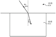
n1sinθ1=n2sinθ2 (1)n 1 sinθ 1 =n 2 sinθ 2 (1)
材料810可具有折射率n1,并且材料812可具有折射率n2,其中折射率n1可以不同于折射率n2。光线可以入射角θ1入射在材料810至材料812的界面处。由于两种材料之间的折射率差值,光线可折射并且可以不同于入射角θ1的折射角θ2进入材料812。如果材料810的折射率小于材料812的折射率,则可减小折射角θ2(即,接近法向入射)。Material 810 may have an index of refraction n 1 , and material 812 may have an index of refraction n 2 , where index of refraction n 1 may be different from index of refraction n 2 . Light rays may be incident at the interface of material 810 to material 812 at an angle of incidence θ 1 . Due to the difference in refractive index between the two materials, light rays are refracted and can enter material 812 at a refraction angle θ 2 that is different from the angle of incidence θ 1 . If the index of refraction of material 810 is less than the index of refraction of material 812, the angle of refraction [theta] 2 can be reduced (ie, near normal incidence).
采用足够高的光功率,光学器件单元可充当浸没物镜。浸没物镜可以是其中光学器件和样本被包围或浸没在具有对比折射率的介质中的系统。对比折射率可比非浸没(例如,光学器件和样本被空气所包围)系统导致降低的有效NA的更大变化。降低的有效NA的较大变化可导致更多的光折射,这可减小光学像差并且可得到更好的测量精度。光学浸没也可消除或减少系统的外部界面(例如,系统接触样本的界面)处的TIR,这可导致更多的光到达检测器。由于更多光到达检测器,系统中包括的光源可以较少的功率被驱动,因此系统可能需要较少的功率。With a sufficiently high optical power, the optics unit can act as an immersion objective. Immersion objectives can be systems in which the optics and sample are surrounded or immersed in a medium with a contrasting index of refraction. The contrast index can result in a larger change in reduced effective NA than a non-immersion (eg, optics and sample surrounded by air) system. Larger changes in reduced effective NA can result in more light refraction, which can reduce optical aberrations and result in better measurement accuracy. Optical immersion can also eliminate or reduce TIR at the external interface of the system (eg, the interface where the system contacts the sample), which can result in more light reaching the detector. Since more light reaches the detector, the light sources included in the system can be driven with less power, and thus the system may require less power.
此外,光学器件单元与样本的紧密接近度可允许系统采用良好限定的(即,明确的和有区别的)界面诸如系统的外部界面(例如,系统接触样本的界面)作为参考。系统可能需要准确地参考样本的“开始”或“边缘”以便重新成像和解析样本内的多个光学路径。当系统的外部界面(例如,系统接触样本的界面)作为参考时,可能需要较少的光学元件或部件(例如,单独的窗口),因为另外还可能需要另外的光学部件来形成良好限定的界面。较少的光学部件可得到更紧凑的系统。Furthermore, the close proximity of the optics unit to the sample may allow the system to take as a reference a well-defined (ie, unambiguous and distinct) interface such as the external interface of the system (eg, the interface where the system contacts the sample). The system may need to accurately reference the "start" or "edge" of the sample in order to re-image and resolve multiple optical paths within the sample. When the external interface of the system (eg, the interface where the system contacts the sample) is used as a reference, fewer optical elements or components (eg, separate windows) may be required, as additional optical components may be required to form a well-defined interface . Fewer optical components result in a more compact system.
除了将设备定位成靠近(例如,触摸)样本之外,样本的测量区域可影响系统的准确地重新成像和解析样本内的多个光学路径的能力。可影响准确重新成像和解析的一个因素可为测量路径长度。测量路径长度可基于目标(例如,预先确定的)路径长度来选择,该目标路径长度可为使得由检测器测得的光谱信号准确地表示样本的所需的一个或多个属性的路径长度。目标测量路径长度可基于样本的刻度长度来确定。样本的刻度长度可基于样本中的平均吸收长度和样本中的减小的散射长度。In addition to positioning the device close to (eg, touching) the sample, the measurement area of the sample can affect the system's ability to accurately re-image and resolve multiple optical paths within the sample. One factor that can affect accurate re-imaging and resolution can be the measurement path length. The measurement path length may be selected based on a target (eg, predetermined) path length, which may be a path length such that the spectral signal measured by the detector accurately represents the desired property or properties of the sample. The target measurement path length can be determined based on the scale length of the sample. The scale length of the sample may be based on the average absorption length in the sample and the reduced scattering length in the sample.
样本中的平均吸收长度可为光可在其上衰减的距离。如果测量路径长度大于平均吸收长度,则可减小剩余的信号(即,尚未散射的信号)或所测量的信号强度,而任何噪声源可能不会衰减相等的量。由于衰减的不平衡,SNR可以较低。平均吸收长度可由比尔-朗伯定律定义,该定律可数学描述在给定波长下样本中的物质对光的吸光度A:The average absorption length in a sample can be the distance over which light can attenuate. If the measured path length is greater than the average absorption length, the remaining signal (ie, the signal that has not been scattered) or the measured signal strength may be reduced, while any noise source may not attenuate by an equal amount. Due to the imbalance of attenuation, the SNR can be lower. The mean absorption length can be defined by the Beer-Lambert law, which mathematically describes the absorbance A of light by a substance in a sample at a given wavelength:
A=ecL (2)A=ecL (2)
其中e为摩尔吸光系数(其可随波长而变化),L为光需要行进穿过样本的路径长度,并且c为所关注物质的浓度。where e is the molar absorption coefficient (which can vary with wavelength), L is the path length that light needs to travel through the sample, and c is the concentration of the species of interest.
如果背景吸光度(即,与所关注物质不同的物质的吸光度)较高,则光需要行进穿过样本的路径长度可小于平均吸收长度。如果背景吸光度是可忽略的,则路径长度可与平均吸收长度相同。本领域的技术人员将理解,相同的路径长度可包括导致15%的偏差的公差。在一些示例中,可选择平均吸收长度,使得平均吸收长度大于或等于光需要行进穿过样本的路径长度。If the background absorbance (ie, the absorbance of a substance other than the substance of interest) is high, the path length that light needs to travel through the sample may be less than the average absorption length. If the background absorbance is negligible, the path length can be the same as the mean absorption length. Those skilled in the art will understand that the same path length may include a tolerance that results in a 15% deviation. In some examples, the average absorption length may be selected such that the average absorption length is greater than or equal to the path length that light needs to travel through the sample.
减小的散射长度可以是关于光学路径的信息在其上丢失的距离(即,随机的或不相关的)。减小的散射长度可通过下式来确定:The reduced scattering length may be the distance over which information about the optical path is lost (ie, random or uncorrelated). The reduced scattering length can be determined by:
μs'=μs(1-g) (3)μ s ′ = μ s (1-g) (3)
其中1/μs为散射事件之间的平均自由路径,并且g为散射各向异性。如果测量路径长度大于减小的散射长度,则测量精度可受到影响。在一些示例中,可选择测量路径长度,使得测量路径长度小于减小的散射长度。where 1/ μs is the mean free path between scattering events and g is the scattering anisotropy. If the measurement path length is greater than the reduced scattering length, the measurement accuracy can be affected. In some examples, the measurement path length may be selected such that the measurement path length is less than the reduced scattering length.
在一些示例中,平均吸收长度可不同于减小的散射长度,并且测量路径长度可基于平均吸收长度和减小的散射长度中的较小者来选择。在一些示例中,平均吸收长度可为短的,或者样本中光的吸光度可为强的,使得反射光的信号未被检测到,并且系统可被配置为增加光源的光功率或增加检测器用于补偿的灵敏度。在一些示例中,该补偿的量可基于功率消耗、对样本的光损伤、样本中不希望的热效应、对光子散粒噪声的效应、检测到的尚未透射穿过样本的杂散光或效应的任何组合。因此,测量路径长度的选择不仅可影响测量精度,而且还影响系统的功率消耗、可靠性以及寿命。In some examples, the average absorption length may be different from the reduced scattering length, and the measurement path length may be selected based on the lesser of the average absorption length and the reduced scattering length. In some examples, the average absorption length may be short, or the absorbance of light in the sample may be strong, such that the signal of reflected light is not detected, and the system may be configured to increase the optical power of the light source or increase the detector for Compensated sensitivity. In some examples, the amount of compensation may be based on any of power consumption, photodamage to the sample, unwanted thermal effects in the sample, effects on photon shot noise, detected stray light that has not yet transmitted through the sample, or effects combination. Therefore, the choice of measurement path length can affect not only the measurement accuracy, but also the power consumption, reliability, and lifetime of the system.
除此之外或另选地,例如,系统可被配置为利用当样本的光学参数随波长变化(例如,超过10%)时的有效刻度长度。有效刻度长度可通过计算每个波长的各个刻度长度来确定,并且对在所关注的波长范围内的各个刻度长度取平均值。在一些示例中,可计算每个波长的各个刻度长度以确定各个刻度长度的范围。系统可被配置为选择最小刻度长度(在各个刻度长度的范围内)、最大刻度长度(在各个刻度长度的范围内),或最小刻度长度和最大刻度长度之间的任何刻度长度。在一些示例中,测量路径长度可基于平均吸收长度、减少的散射长度、最小刻度长度、最大刻度长度或任何组合来选择。Additionally or alternatively, for example, the system may be configured to utilize the effective graticule length when the optical parameter of the sample varies with wavelength (eg, by more than 10%). The effective tick length can be determined by calculating the individual tick lengths for each wavelength, and averaging the individual tick lengths over the wavelength range of interest. In some examples, the individual tick lengths for each wavelength can be calculated to determine the range of the individual tick lengths. The system may be configured to select a minimum tick length (within a range of individual tick lengths), a maximum tick length (within a range of individual tick lengths), or any tick length between the minimum and maximum tick lengths. In some examples, the measurement path length may be selected based on an average absorption length, a reduced scattering length, a minimum scale length, a maximum scale length, or any combination.
如上所述,刻度长度可用于确定样本上测量区域的大小。测量区域外的光可为已经历过样本内的多次随机散射事件的光线,并且因此,这些光线可与在样本内行进的光学路径不相关。不相关的光线可能不会为准确测量提供有用信息,并且因此可被丢弃或忽略而不牺牲准确测量。As mentioned above, the scale length can be used to determine the size of the measurement area on the sample. Light outside the measurement area may be rays that have undergone multiple random scattering events within the sample and, thus, may be uncorrelated with the optical path traveled within the sample. Irrelevant rays may not provide useful information for accurate measurements, and can therefore be discarded or ignored without sacrificing accurate measurements.
例如,所关注的波长可在1500nm至2500nm之间(即,SWIR范围),并且在所关注波长上平均的平均吸收长度和减小的散射长度可为1mm,其可对应于1mm的刻度长度。该刻度长度可对应于直径为1至2mm的用于收集离开样本的光的样本区域。即,离开样本的大部分(例如,大于70%)光功率可在该1至2mm直径的区域内浓缩,并且该区域之外的离开样本的光线可被忽略。For example, the wavelength of interest may be between 1500 nm and 2500 nm (ie, the SWIR range), and the average absorption length and reduced scattering length averaged over the wavelength of interest may be 1 mm, which may correspond to a 1 mm scale length. The scale length may correspond to a sample area of 1 to 2 mm in diameter for collecting light exiting the sample. That is, most (eg, greater than 70%) of the optical power leaving the sample can be concentrated in this 1 to 2 mm diameter region, and light leaving the sample outside this region can be ignored.
刻度长度也可用于确定从输出耦合器发射的输入光束的大小。光束的大小可影响光功率(即,光学强度)和衍射效应。测量精度可有利于准直输入光束,以便系统以足够的光功率(例如,具有可被检测器检测到的足够高SNR的信号)和最小的衍射效应操作。例如,1mm的刻度长度可对应于光束直径在100μm至300μm之间的准直输入光束。在一些示例中,该输入光束可配置为具有小于175μm的光束直径。The scale length can also be used to determine the size of the input beam emitted from the output coupler. The size of the beam can affect optical power (ie, optical intensity) and diffraction effects. Measurement accuracy may facilitate collimating the input beam so that the system operates with sufficient optical power (eg, a signal with a sufficiently high SNR to be detected by the detector) and minimal diffraction effects. For example, a scale length of 1 mm may correspond to a collimated input beam with a beam diameter between 100 μm and 300 μm. In some examples, the input beam may be configured to have a beam diameter of less than 175 μm.
与输入光束的属性类似,光学器件单元的属性也可影响系统。光学器件单元可在单个衬底或层上形成,或者可在两个或多个衬底或层上形成。在一些示例中,光学器件单元、检测器阵列、光源或任何组合可安装到相同的光学平台上。在一些示例中,光学器件单元可具有接触样本的平的(即,平坦的)表面。用平的表面配置光学器件可减少晶片处理和制造复杂性。在一些示例中,另一表面(即,与样本相对的表面)可为凸面的以增强光学功率。在一些示例中,该另一表面可为单凸面折射表面。在一些示例中,光学器件单元的厚度可基于光弯曲的量。在一些示例中,该厚度可在100μm至300μm之间。Similar to the properties of the input beam, the properties of the optics unit can also affect the system. The optics unit may be formed on a single substrate or layer, or may be formed on two or more substrates or layers. In some examples, optics units, detector arrays, light sources, or any combination may be mounted on the same optical table. In some examples, the optics unit may have a flat (ie, flat) surface that contacts the sample. Configuring optics with flat surfaces reduces wafer handling and manufacturing complexity. In some examples, the other surface (ie, the surface opposite the sample) may be convex to enhance optical power. In some examples, the other surface may be a monoconvex refractive surface. In some examples, the thickness of the optics unit may be based on the amount of light bending. In some examples, the thickness may be between 100 μm and 300 μm.
图9A至图9B示出了根据本公开的示例的示例性光学器件单元的俯视图和透视图。组900可包括多个单元,每个单元包括至少三个区域:发射区域916、参考区域922和测量区域929。9A-9B illustrate top and perspective views of exemplary optics units according to examples of the present disclosure.
发射区域916可被配置为防止任何镜面反射到达检测器阵列。发射区域916可包括能够阻挡或吸收光的阻光器或光吸收器。在一些示例中,阻光器可包括防止入射光反射的任何材料(例如,防反射涂层)。在一些示例中,阻光器可包括在与检测器阵列的检测波长不同的波长下反射的任何材料。在一些示例中,发射区域可包括不透明掩模。The
参考区域922可包括被配置用于扩散入射光束的任何类型的光学器件(例如,负微透镜)。从光源发射的光可被引导到参考(例如,包括在系统200中的参考222),其可将光中继到参考区域922。参考区域922可扩散该光,使得一个或多个光束被引导到检测器阵列上的检测器像素。在一些示例中,参考区域922可包括负透镜或者说焦距为负的透镜。在一些示例中,参考区域922可包括棱镜。在一些示例中,参考区域922可包括用于检测器阵列中的每个检测器像素的不同棱镜楔。在一些示例中,参考区域922可包括分束器。在一些示例中,参考区域922可被配置为将光扩散成或分成多个光束。在一些示例中,参考区域922可被配置为均匀扩散光使得每个光束的一个或多个属性是相同的。本领域的技术人员将理解,相同的属性可包括导致15%的偏差的公差。在一些示例中,参考区域922可被配置为使光束扩散,使得至少两个光束的强度不同。在一些示例中,参考区域922可包括多个光学器件。在一些示例中,包括在参考区域922中的光学器件的大小和/或形状可基于检测器像素的数量和/或离开参考区域922的一个或多个光束的属性。在一些示例中,一个或多个孔隙层可位于参考区域922中以控制离开参考区域922的光的属性和/或方向。
测量区域929可包括一个或多个收集光学器件(例如,正微透镜)。收集光学器件可被配置为重新成像和解析样本中的多个光学路径,如上所述。该系统可被配置为在从光源发射光以入射在参考区域922上和从光源发射光以入射在测量区域929上之间切换或交替。收集光学器件的属性将在下文中讨论。
虽然图4A至图7示出了包括系统的单元,其中每个单元可包括来自输出耦合器的离开样本并由共轭光学系统和检测器阵列收集的一个光束,但是本公开的实施例包括具有多个单元的系统。图9C示出了根据本公开的实施例包括在系统中的多个组中的示例性光学器件单元和检测器阵列的俯视图。该系统可包括耦合到检测器阵列930的多个组900。在一些示例中,包括在测量区域929中的一个或多个光学器件可在相邻组900之间“共享”。在一些示例中,系统可配置有一个或多个具有光源的组,所述光源交替向共享光学器件发射光。在一些示例中,系统可配置有27个组900和9×3检测器阵列930。在一些示例中,每个组900可与另一个组900间隔开至少2mm。尽管图9A至图9B示出了布置有参考区域922的组900,该参考区域位于发射区域916和包括在测量区域929中的3×3光学器件的网格之间,但是本公开的示例可包括三个区域的任何布置和包括在测量区域929中的光学器件的任何布置。例如,发射区域916可位于组900的中心中,并且这些光学器件可围绕发射区域916的外边缘。While FIGS. 4A-7 show units comprising systems, where each unit may comprise one beam from an output coupler exiting the sample and collected by a conjugate optical system and detector array, embodiments of the present disclosure include having system of multiple units. 9C shows a top view of an exemplary optics unit and detector array included in multiple groups in a system according to an embodiment of the present disclosure. The system may include a plurality of
如上所述,光学器件单元中所包括的光学器件的配置和属性可基于多种因素。这些属性可包括有效焦距、工作距离、光学器件的材料、填充因子、孔径大小、间距、倾斜度(或偏心)以及取向(或旋转度),如将要讨论的。As mentioned above, the configuration and properties of the optics included in the optics unit may be based on a variety of factors. These properties may include effective focal length, working distance, material of the optics, fill factor, aperture size, spacing, tilt (or decentering), and orientation (or rotation), as will be discussed.
基于收集角度范围与光线入射到的检测器(或检测器像素)表面上的位置之间的关系,该系统可配置为具有有效焦距。该系统还可基于检测器阵列的集成配置。The system can be configured to have an effective focal length based on the relationship between the range of collection angles and the location on the detector (or detector pixel) surface where the light is incident. The system can also be based on an integrated configuration of detector arrays.
由于光学器件单元位于样本与检测器之间的路径中,光学器件的材料可影响所检测到的光的光学属性,进而影响测量精度。为了允许离开样本的光到达检测器阵列,该光学器件可被配置为具有在所关注的波长范围内透明的材料以使得可防止光被反射离开光学器件的表面。另外,在光学器件单元与样本接触的示例中,光学器件的材料可基于光学器件化学和物理暴露于样本时材料降解的抗性。此外,可以考虑其他考虑因素,诸如与用于产生光学器件单元的任何图案(例如,蚀刻轮廓)的晶片级处理的兼容性、材料的可用性和成本。Since the optics unit is in the path between the sample and the detector, the material of the optics can affect the optical properties of the detected light, which in turn affects the measurement accuracy. To allow light exiting the sample to reach the detector array, the optics can be configured with a material that is transparent in the wavelength range of interest so that light can be prevented from being reflected off the surface of the optics. Additionally, in examples where the optics unit is in contact with the sample, the material of the optics may be based on the resistance of the optics to degradation of the material upon chemical and physical exposure to the sample. Additionally, other considerations may be considered, such as compatibility with wafer-level processing for producing any pattern (eg, etch profile) of optical device cells, availability of materials, and cost.
也可基于样本的折射率来选择光学器件单元的材料。例如,当样本的折射率为1.42(或在10%以内)时,系统可被配置为具有折射率为3.4(或在10%以内)的光学器件单元(例如,硅透镜的单元)。入射光在系统的外部界面(例如,系统与样本接触的界面)处的入射角可为45°,从而可产生16.9°的折射角。以这种方式,可选择光学器件单元的材料,使得检测器阵列表面上的入射角可以更接近法向,这可使检测器接收更高的光功率,得到更好的测量精度,以及可被配置用于更低的功率消耗的系统。The material of the optics unit can also be selected based on the refractive index of the sample. For example, when the index of refraction of the sample is 1.42 (or within 10%), the system may be configured with an optics cell (eg, a cell of a silicon lens) having an index of refraction of 3.4 (or within 10%). The angle of incidence of the incident light at the external interface of the system (eg, the interface of the system in contact with the sample) may be 45°, resulting in a refraction angle of 16.9°. In this way, the material of the optics unit can be selected so that the angle of incidence on the detector array surface can be closer to the normal, which allows the detector to receive higher optical power, resulting in better measurement accuracy, and can be Configure the system for lower power consumption.
此外,可选择光学器件单元的材料,使得光线发生更少的“扩散”(即,系统的外部界面(例如,系统与样本接触的界面)和检测器的表面之间的光束的分散)。例如,入射到系统的外部界面(例如,系统与样本接触的界面)上且入射角为60°的光可得到20.9°的折射角。在光学器件单元和样本之间没有折射率对比的情况下,扩散将为15°(即,60°-45°),而在光学器件单元和样本之间有折射率对比的情况下,光线的扩散可为4°(即,20.9°-16.9°)。光线的较小扩散可产生较窄范围的收集角度,这可得到较小的光学器件和更紧凑的系统。In addition, the materials of the optics unit can be selected so that less "spread" of the light occurs (ie, the dispersion of the light beam between the external interface of the system (eg, the interface between the system and the sample) and the surface of the detector). For example, light incident on an external interface of the system (eg, the interface between the system and the sample) with an angle of incidence of 60° would result in a refraction angle of 20.9°. In the absence of refractive index contrast between the optics unit and the sample, the diffusion will be 15° (ie, 60°-45°), while with the refractive index contrast between the optics unit and the sample, the Diffusion may be 4° (ie, 20.9°-16.9°). Smaller spread of light can result in a narrower range of collection angles, which can result in smaller optics and a more compact system.
在一些示例中,感兴趣的波长范围可以是SWIR(即,1500nm-2500nm),并且光学器件单元可以包括单晶硅、蓝宝石、熔融二氧化硅、氧化物玻璃、硫属化物玻璃、砷化镓(GaAs)、硒化锌(ZnSe)、锗(Ge)或这些材料的任何组合。In some examples, the wavelength range of interest may be SWIR (ie, 1500nm-2500nm), and the optics unit may include monocrystalline silicon, sapphire, fused silica, oxide glass, chalcogenide glass, gallium arsenide (GaAs), zinc selenide (ZnSe), germanium (Ge), or any combination of these materials.
光学器件的直径可以基于从光源发射的光束的尺寸。例如,光束直径配置在100–300μm之间的系统也可以将光学器件单元的直径配置在100–300μm之间。The diameter of the optics may be based on the size of the light beam emitted from the light source. For example, systems with beam diameters configured between 100–300 μm can also have optics units configured with diameters between 100–300 μm.
光学器件单元的填充因子可以表示从收集的样本离开的光线的百分比或分数。通常,入射光束的扩散减少可导致光学器件单元处的填充因子变大(即,导向检测器的光的面积与光学器件的总面积的比率),并且因此可导致更高的光学效率。光学元件的填充因子可以通过以下方式确定:The fill factor of an optics cell can represent the percentage or fraction of light that exits the collected sample. In general, reduced spread of the incident beam can lead to a larger fill factor at the optics unit (ie, the ratio of the area of light directed to the detector to the total area of the optics), and thus can lead to higher optical efficiency. The fill factor of an optical element can be determined by:

其中AD是孔径尺寸。透镜或微透镜的填充因子FF可以表示从样本离开、折射到系统中然后通过孔径透射的光量。在一些示例中,与包括在光学器件单元中的光学器件相关联的孔径的孔径尺寸,可以基于入射光线的扩散。入射光线的扩散量较少时,可以减小孔径尺寸和光学器件间距,使得实现高填充因子而不损失包括相关信息(例如,可以有助于获得更好的测量精度的信息)的入射光线。在一些示例中,光学器件单元可以配置25%或更大的填充因子FF。在一些示例中,光学器件单元可以配置50%或更大的填充因子FF。在一些示例中,光学器件单元可以配置60%或更大的填充因子FF。where AD is the aperture size. The fill factor FF of a lens or microlens can represent the amount of light that leaves the sample, is refracted into the system, and then transmitted through the aperture. In some examples, the aperture size of the apertures associated with the optics included in the optics unit may be based on the spread of incident light rays. With less spread of incident light, aperture size and optics spacing can be reduced so that high fill factors are achieved without loss of incident light including relevant information (eg, information that may contribute to better measurement accuracy). In some examples, the optics unit may be configured with a fill factor FF of 25% or greater. In some examples, the optics unit may be configured with a fill factor FF of 50% or greater. In some examples, the optics unit may be configured with a fill factor FF of 60% or greater.
光学器件单元的间距可以是相邻光学器件之间的距离,对光学器件的尺寸有影响。在一些示例中,间距可以基于光学器件单元的填充因子。如等式4所示,光学器件单元的填充因子可以与孔径尺寸相关,因此光学器件单元的间距也可以基于孔径尺寸。为了增加填充因子和捕获从样本离开的光线的效率,间距可以大于孔径尺寸。例如,对于100μm–300μm之间的孔径尺寸,光学器件可以配置为具有125μm–500μm之间的间距。在一些示例中,孔径尺寸可以配置为直径175μm,间距可以是250μm,填充因子可以是38.4%。The pitch of the optical device units may be the distance between adjacent optical devices, which has an effect on the size of the optical devices. In some examples, the pitch may be based on the fill factor of the optics cells. As shown in Equation 4, the fill factor of the optics cells can be related to the aperture size, so the spacing of the optics cells can also be based on the aperture size. To increase the fill factor and the efficiency of capturing light exiting the sample, the spacing can be larger than the aperture size. For example, for aperture sizes between 100 μm–300 μm, the optics can be configured with a pitch between 125 μm–500 μm. In some examples, the aperture size may be configured to be 175 μm in diameter, the pitch may be 250 μm, and the fill factor may be 38.4%.
除此之外或另选地,光学器件间距和孔径尺寸可以基于收集角的范围。孔径尺寸可以确定从样本离开的光线中哪些被光学器件接受(即,穿过检测器传输),哪些被拒绝(即,被阻止到达检测器)。样本材料和样本中的物质可导致高散射各向异性。结果,集光效率(即,收集散射光的效率)可以基于收集角的范围。虽然收集角越宽可以导致收集的光越多(即,光学功率更高),但是收集的光会包括更大比例的不需要的光(例如,噪声或不相关的光)。不同角度的收集光线可以对精确测量有不同的重要性或相关性。在一些示例中,当光偏离检测器表面上的法向入射(例如,大于70°)时,光线的光功率可以更低。入射角偏离偏离法向入射的光线可以包括与光源发出的光具有较小交叉角的光线(这可以导致散射位置或路径长度的较大不确定性)和具有大量散射事件的光线。结果,入射角偏离法向入射的光线可能不大相关并且可能导致测量不大准确。此外,偏离法向入射的光线可包括从样本内浅处的位置散射的光。在一些应用中,在样本中关注的物质可以位于样本的深处,因此从样本内浅处位置散射的光线可能不会为测量提供相关信息。Additionally or alternatively, optics pitch and aperture size may be based on a range of collection angles. Aperture size can determine which of the light exiting the sample is accepted by the optics (ie, transmitted through the detector) and which is rejected (ie, prevented from reaching the detector). The sample material and species in the sample can cause high scattering anisotropy. As a result, the collection efficiency (ie, the efficiency of collecting scattered light) can be based on a range of collection angles. While wider collection angles may result in more light being collected (ie, higher optical power), the collected light may include a greater proportion of unwanted light (eg, noise or irrelevant light). Different angles of collected light can have different importance or relevance for accurate measurements. In some examples, the optical power of the light may be lower when the light is deviated from normal incidence on the detector surface (eg, greater than 70°). Incidence angle deviations Light rays that deviate from normal incidence can include rays that have a small angle of intersection with the light emitted by the light source (which can lead to large uncertainties in scattering position or path length) and rays that have a large number of scattering events. As a result, rays with angles of incidence that deviate from normal incidence may be less correlated and may result in less accurate measurements. Additionally, off-normal incidence light rays may include light scattered from shallow locations within the sample. In some applications, the species of interest in the sample may be located deep within the sample, so light scattered from shallow locations within the sample may not provide relevant information for the measurement.
受收集角范围影响的可以是孔径尺寸、光学或光学间距、收集效率、入射在检测器上的光功率,以及系统的功率。系统可以配置测量的收集角范围可以基于目标(例如,预定的)收集角范围。目标收集角范围可以基于几个因素来确定,诸如收集效率、几何路径不确定性、样本中可能发生的散射事件的数量、穿透深度和光学设计的限制,光学设计可以基于光线的路径长度确定。为了确定光线的路径长度,可以考虑存在的多个不确定性。总路径长度不确定性ΔPL可包括空间分辨率不确定性Δspatial、角分辨率不确定性Δangular、输入高斯角度发散度Δinput和低角度样本散射不确定性Δmultiple_scatter,可以定义为:Affected by the collection angle range can be aperture size, optical or optical spacing, collection efficiency, optical power incident on the detector, and system power. The collection angle range that the system may configure for the measurement may be based on a target (eg, predetermined) collection angle range. The target collection angle range can be determined based on several factors such as collection efficiency, geometric path uncertainty, number of possible scattering events in the sample, penetration depth and limitations of optical design, which can be determined based on the path length of the light rays . To determine the path length of a ray, a number of uncertainties exist that can be considered. The total path length uncertainty ΔPL can include the spatial resolution uncertainty Δspatial, the angular resolution uncertainty Δangular, the input Gaussian angle divergence Δinput, and the low-angle sample scattering uncertainty Δmultiple_scatter, and can be defined as:
ΔPL2=(Δspatial)2+(Δangular)2+(Δinput)2+(Δmultiple_scatter)2(5)ΔPL 2 =(Δspatial) 2 +(Δangular) 2 +(Δinput) 2 +(Δmultiple_scatter) 2 (5)
系统中的一个或多个光学器件和孔隙层的属性可以基于空间分辨率不确定性来配置。图10示出了根据本公开的示例的具有空间分辨率不确定性的光线的示例性配置。系统1000可以接触或靠近样本1020。光可以在位置1006处离开系统1000并且可以穿过样本1020行进长度d11,到达位置1010。位置1010处的光入射角可以是入射角θ1。一部分光可以以散射角θ4散射,穿过样本1020行进长度d12,并且可以到达位置1016处的系统的外部界面(例如,系统接触样本的界面)。位置1006和位置1016之间的距离可以称为距离x。另一部分光可以进一步行进到样本1020中,行进总长度d21,到达位置1040。在一些示例中,位置1040处的光的入射角也可以是入射角θ1并且光也可以以散射角θ- 4散射。散射光可以穿过样本1020行进长度d22,并且可以到达系统的外部界面(例如,系统接触样本的界面)的位置1046处。位置1016和位置1046之间的空间分辨率或距离可以称为空间分辨率或距离Δx。Properties of one or more optics and aperture layers in the system can be configured based on spatial resolution uncertainty. 10 illustrates an example configuration of rays with spatial resolution uncertainty according to an example of the present disclosure. The
空间分辨率不确定性Δspatial可以基于在位置1016处入射的散射光与在位置1046处入射的散射光之间的光学路径长度的差异,并且可以定义为:The spatial resolution uncertainty Δspatial can be based on the difference in optical path length between the scattered light incident at
Δspatial=d21+d22-d11-d12 (6)Δspatial=d 21 +d 22 -d 11 -d 12 (6)
根据正弦定律:According to the law of sine:


因此,空间分辨率不确定性Δspatial可以减小到:Therefore, the spatial resolution uncertainty Δspatial can be reduced to:

如等式12所示,空间分辨率不确定性Δspatial可以随入射角θ1而减小,散射角θ4可以增大。另外,空间分辨率不确定性Δspatial可以随着空间分辨率Δx(即,在位置1016处入射的光与在位置1046处入射的光之间的距离)而增大。在一些示例中,可以基于空间分辨率不确定性Δspatial来配置光学器件的孔径尺寸、倾斜度或取向,或它们的组合。在一些示例中,空间分辨率不确定性Δspatial可以在150μm-200μm之间,可以与入射角θ1=45°和45°的收集角(可以等于散射角θ4)相同。As shown in Equation 12, the spatial resolution uncertainty Δspatial can decrease with the incident angle θ 1 and the scattering angle θ 4 can increase. Additionally, the spatial resolution uncertainty Δspatial may increase with the spatial resolution Δx (ie, the distance between the light incident at
系统中的一个或多个光学器件的属性也可以基于空间分辨率不确定性来配置。图11示出了根据本公开的示例的具有角分辨率不确定性的光线的示例性配置。系统1100可以接触或靠近样本1120。光可以在位置1106处离开系统1100并且可以穿过样本1120行进长度d11,到达位置1110。位置1110处的入射角可以是入射角θ1。一部分光可以以散射角θ5从位置1110处散射,穿过样本920行进长度d12,并且可以到达系统的外部分界面(例如,系统接触样本的分界面)的位置1146处。系统的外部界面(例如,系统与样本接触的界面)处折射率的改变可导致折射角θ8。另一部分光可以进一步行进到样本1120中,行进总长度d21,到达位置1140。在一些示例中,位置1140处的光的入射角也可以是入射角θ1并且从位置1140处散射的光也可以具有散射角θ6。在一些示例中,散射角θ6可以与散射角θ1不同。从位置1140处散射的光可以穿过样本1120行进长度d22,并且可以到达系统的外部界面(例如,系统接触样本的界面)的位置1146处。系统的外部界面(例如,系统与样本接触的界面)处折射率的改变可导致折射角θ7。位置1106和位置1146之间的距离可以称为距离x。在一些示例中,折射角θ8可以与折射角θ7不同,差值为角分辨率Δθ。Properties of one or more optics in the system can also be configured based on spatial resolution uncertainty. 11 illustrates an exemplary configuration of rays with angular resolution uncertainty according to an example of the present disclosure. The system 1100 can be in contact with or near the sample 1120. Light may exit system 1100 at location 1106 and may travel length d 11 through sample 1120 to location 1110 . The angle of incidence at location 1110 may be the angle of incidence θ 1 . A portion of the light may be scattered from location 1110 at scattering angle θ 5 , travel length d 12 through sample 920 , and may reach location 1146 where the system's external interface (eg, the interface where the system contacts the sample). Changes in the refractive index at the external interface of the system (eg, the interface where the system contacts the sample) can result in a refraction angle θ 8 . Another portion of the light may travel further into sample 1120 , for a total length d 21 , to location 1140 . In some examples, the angle of incidence of the light at location 1140 may also be an angle of incidence θ 1 and light scattered from location 1140 may also have a scattering angle θ 6 . In some examples, the scattering angle θ 6 may be different from the scattering angle θ 1 . Light scattered from location 1140 may travel length d 22 through sample 1120 and may reach location 1146 where the system's external interface (eg, the interface where the system contacts the sample). Changes in refractive index at the external interface of the system (eg, the interface where the system contacts the sample) can result in a refraction angle θ 7 . The distance between location 1106 and location 1146 may be referred to as distance x. In some examples, the refraction angle θ 8 may be different from the refraction angle θ 7 by the angular resolution Δθ.
角分辨率的不确定性Δangular可以基于两个散射光束(例如,从位置1110处散射的光和从位置1140处散射的光)之间的折射角的差异,并且可以定义为:The uncertainty in angular resolution, Δangular, can be based on the difference in the angle of refraction between the two scattered beams (eg, the light scattered from location 1110 and the light scattered from location 1140 ), and can be defined as:
Δangular=d21+d22-d11-d12 (13)Δangular=d 21 +d 22 -d 11 -d 12 (13)
根据正弦定律和斯内尔定律:According to the law of sine and Snell's law:


因此,角分辨率不确定性Δangular可以减小到:Therefore, the angular resolution uncertainty Δangular can be reduced to:

如等式18所示,角分辨率不确定性Δangular随着从光源发出的光与出射位置之间的距离x的增大而增大。在一些示例中,系统可以配置为具有基于角分辨率不确定性Δangular的光源和包括在光学器件单元中的对应光学器件之间的距离。在一些示例中,系统可以配置为具有基于角分辨率不确定性Δangular的收集角范围(即,角度区间)。在一些示例中,可以基于空间分辨率不确定性Δspatial来配置光学器件的倾斜度、取向,或它们两者。在一些示例中,角度分辨率不确定性可以在40μm–100μm之间,收集角的范围可以在5°–10°之间。As shown in Equation 18, the angular resolution uncertainty Δangular increases as the distance x between the light emitted from the light source and the exit location increases. In some examples, the system may be configured to have a distance between a light source and a corresponding optics included in the optics unit based on the angular resolution uncertainty Δangular. In some examples, the system may be configured to have a collection angle range (ie, angular interval) based on the angular resolution uncertainty Δangular. In some examples, the tilt, orientation, or both of the optics may be configured based on the spatial resolution uncertainty Δspatial. In some examples, the angular resolution uncertainty may be between 40 μm - 100 μm and the collection angle may range between 5° - 10°.
可以基于高斯角度发散度来配置系统中光束的属性。图12示出了根据本公开的示例的具有高斯角度发散度的输入光束的示例性配置。系统1200可以接触或靠近样本1220。光可以在位置1206处离开系统1200并且可以具有入射角θ1(相对于半角发散度θ12测量)。在一些示例中,从光源发射的光的一部分可以在位置1210处以具有入射角θ10的一部分光发散,并穿过样本1220,行进长度d21,到达位置1210。从光源发射的光的另一部分也可以在位置1210处以入射角θ11发散,并穿过样本1220,行进长度d12,到达位置1210。光可以以散射角θ13从系统的外部界面(例如,系统接触样本的界面)上的位置1210处散射到位置1246处。一部分散射光可以穿过样本1220行进长度d 12,其他部分的散射光可以穿过样本1220行进长度d22。系统的外部界面(例如,系统与样本接触的界面)处折射率的改变可导致折射角θ14。The properties of the beams in the system can be configured based on the Gaussian angular divergence. 12 illustrates an exemplary configuration of an input beam with Gaussian angular divergence according to an example of the present disclosure. The system 1200 can be in contact with or near the sample 1220. Light may exit system 1200 at
高斯角度发散度Δinput可以基于发散光线之间光学路径长度的差异,可以定义为:The Gaussian angle divergence Δinput can be based on the difference in optical path length between divergent rays and can be defined as:
Δinput=d21+d22-d11-d12 (19)Δinput=d 21 +d 22 -d 11 -d 12 (19)
根据正弦定律:According to the law of sine:


随着高斯角度发散度Δinput的增大,路径长度不确定性ΔPL可变成由角分辨率不确定性Δangular主导。在一些示例中,空间分辨率不确定性可以贡献超过路径长度不确定性ΔPL的一半。在一些示例中,系统可以配置为具有包含5-10个角度区间的50°收集角范围。As the Gaussian angular divergence Δinput increases, the path length uncertainty ΔPL can become dominated by the angular resolution uncertainty Δangular. In some examples, the spatial resolution uncertainty may contribute more than half of the path length uncertainty ΔPL. In some examples, the system may be configured to have a 50° collection angle range containing 5-10 angular intervals.
可以基于集光效率来配置光学器件的倾斜度,光学器件的倾斜度可以影响测量精度和系统的功耗。通过倾斜光学器件(即,设置光轴取向)使得收集方向平行于入射光的轴(即,收集方向面向入射光方向),可以提高集光效率。例如,入射光的轴可以是45°,收集方向可以是-45°。在一些示例中,光学器件的倾斜度可基于收集角的范围。例如,收集角的范围可以是0°到-75°,收集方向可以是-37.5°。在一些示例中,收集角的范围可以是-25°到-70°,收集方向可以是-47.5°。在一些示例中,收集角的范围可以是-30°到-60°,收集方向可以是-45°。在一些示例中,光学器件可以包括凸表面,该凸表面可以是倾斜的(或偏心的)以解决收集角度范围内的任何不对称性(即偏置)。对任何不对称性进行补偿可以减小光学器件的光学像差的量值或影响。在一些示例中,所有光学器件可以在法向入射的相同方向上平铺。The tilt of the optics can be configured based on the collection efficiency, which can affect the measurement accuracy and the power consumption of the system. By tilting the optics (ie, orienting the optical axis) so that the collection direction is parallel to the axis of the incident light (ie, with the collection direction facing the incident light direction), light collection efficiency can be improved. For example, the axis of the incident light may be 45° and the collection direction may be -45°. In some examples, the tilt of the optics may be based on a range of collection angles. For example, the collection angle may range from 0° to -75° and the collection direction may be -37.5°. In some examples, the collection angle may range from -25° to -70° and the collection direction may be -47.5°. In some examples, the collection angle may range from -30° to -60° and the collection direction may be -45°. In some examples, the optics may include a convex surface, which may be sloped (or eccentric) to account for any asymmetry (ie, offset) in the collection angle range. Compensating for any asymmetry can reduce the magnitude or effect of optical aberrations of the optic. In some examples, all optics may be tiled in the same direction of normal incidence.
除光学器件外,系统性能还会受到系统中包括的一个或多个其他部件的属性的影响。在一些示例中,系统可包括位于光学器件单元和光学平台之间的间隔件。在一些示例中,光学器件单元和光学平台可包括单晶硅。在一些示例中,光源、光学迹线或两者可包括在光学平台上形成的硅波导。在一些示例中,耦合到检测器的ROIC可以在硅上制造。通过将光学器件单元、光学平台和ROIC中的一个或多个配置为包括硅,部件的热膨胀可以是类似的,这可以最小化任何机械弱点,并且可以提高系统的稳健性。另外,硅可以是具有许多所需属性的材料,诸如良好的机械强度、良好的导热性、低成本和良好的可靠性。In addition to optics, system performance can be affected by the properties of one or more other components included in the system. In some examples, the system may include a spacer between the optics unit and the optical table. In some examples, the optics unit and the optical table may comprise single crystal silicon. In some examples, the light source, optical traces, or both may include silicon waveguides formed on an optical table. In some examples, the ROIC coupled to the detector can be fabricated on silicon. By configuring one or more of the optics unit, optical table, and ROIC to include silicon, the thermal expansion of the components can be similar, which can minimize any mechanical weaknesses and can improve the robustness of the system. Additionally, silicon can be a material with many desirable properties, such as good mechanical strength, good thermal conductivity, low cost, and good reliability.
在一些示例中,系统可包括位于光学器件和样本之间的光学间隔件窗口。图13A示出了根据本公开的示例的示例性系统的剖视图,该系统包括光学间隔件窗口以及位于光学间隔件窗口和样本之间的孔隙层。系统1300可包括光源1302、光学器件单元1312、孔隙层1386和光学间隔件窗口1321,其中光学间隔件窗口1321可与样本1320接触。光源1302可发射光1352,从样本1320离开。被称为光1354的光可以在样本1320内从位置1357处反射离开,可以穿过孔隙层1386传输,并且可以到达光学器件单元1312。In some examples, the system can include an optical spacer window between the optics and the sample. 13A shows a cross-sectional view of an exemplary system including an optical spacer window and an aperture layer located between the optical spacer window and a sample, according to an example of the present disclosure.
如图13A所示,放置孔隙层1386可导致因边缘界面处散射和光学像差产生的杂散光,这可能降低光学器件单元1312的成像属性。图13B示出了根据本公开的示例的示例性系统的剖视图,该系统包括光学间隔件窗口以及位于光学间隔件窗口和光学器件单元之间的孔隙层。通过位于光学间隔件窗口1321和光学器件单元1312之间的孔隙层1387,光1354可传播到包括在光学器件单元1312中的适当光学器件,并且可减少或消除因边缘界面处散射产生的杂散光。As shown in FIG. 13A, placement of the
在一些示例中,光学间隔件窗口1321可为多功能的并且可以被配置为向光学器件提供机械支撑。光学器件单元1312的厚度可基于由光学器件单元1312执行的光弯曲的量以及分离不同折射角的能力来配置。随着光学器件单元1312的厚度减小,光学器件单元1312的性能增加。然而,光学器件单元1312的厚度的减小可导致光学器件单元易碎、昂贵,并且可能需要复杂的制造方案且产率低。该系统可配置成使得光学间隔件窗口1321补偿薄光学器件单元1312的易碎性而不损害光学性能。在一些示例中,光学间隔件窗口1321的厚度可在400μm至700μm之间。在一些示例中,光学间隔件窗口1321的厚度可为650μm。In some examples, the
在一些示例中,光学间隔件窗口1321可被配置为具有这样的厚度,使得可减少样本1320与有源部件(例如,检测器,光源和电子器件)之间的热交换效应。有源部件可产生热量并且还可对任何温度波动敏感,并且样本1320的温度可变化或者可与有源部件的操作温度不同。因此,样本1320温度和有源部件操作温度的差异可导致热交换效应,可降低测量精度。在一些示例中,样本1320可为皮肤,如不减轻热交换效应,则任何温度差异都可能引起不适。In some examples, the
在一些示例中,光学间隔件窗口1321可包括中间涂层(即,具有在样本1320的折射率和光学器件单元1312的折射率之间的折射率的介电材料)。在没有中间涂层的情况下,光学器件单元1312或设置在光学器件单元1312上的任何防反射涂层将被配置成使得光学器件单元1312和样本1320之间具有高折射率对比度或者系统中的折射角将减小。另一方面,包含中间涂层可降低复杂性并增大系统中的折射角。In some examples, the
在一些示例中,光学间隔件窗口1321可包括介电材料。在一些示例中,与光学器件相比,介电材料可具有更高的化学耐久性、更高的物理耐久性或二者皆有。在一些示例中,光学间隔件窗口1321可包括蓝宝石。通过在光学器件和样本之间包括光学间隔件窗口,该系统可具有更高的机械强度、更高的设备耐久性和更低的热交换。In some examples, the
包括光学间隔件窗口1321可改变光在检测器阵列中的光学器件和检测器像素之间分布的方式。然而,可以解释这种改变,并且入射到检测器阵列上的光仍然可以允许每个检测器像素描述样本中的轨迹或光学路径。图14A示出了根据本公开的示例的不包括光学间隔件窗口的示例性系统的剖视图以及相应地确定入射在系统的外部界面(例如,系统接触样本的界面)处的光的横向位置。系统1400可包括光源1402、光学器件单元1412、孔隙层1486和检测器阵列1430。光源1402可在位置1406处发射离开样本1420的光1452。光1453、光1454和光1455可在样本1420内的位置1457处反射离开并且可以在位置1446处入射到系统的外部界面(例如,系统接触样本的界面),该位置1446可距离位置1406处x距离。光1453,光1454和光1455可透射透过孔隙层1486并且可到达包括在光学器件单元1412中的光学器件1418。检测器阵列1430可包括检测器像素1433、检测器像素1435和检测器像素1437。光1453可入射在检测器像素1433上,光1454可入射在检测器像素1435上,并且光1455可入射在检测器像素1437上。因此,光学器件1418、检测器像素1433、检测器像素1435和检测器像素1437可与位置1446相关联。通过这种方式,入射光在系统的外部界面(例如,系统接触样本的界面)处的横向位置可与包括在光学器件单元中的光学器件相关联。The inclusion of
包含光学间隔件窗口可导致基于包括在光学器件单元中的光学器件和包括在检测器阵列中检测器像素确定入射光在系统外部界面(例如,系统接触样本的界面)处的横向位置。图14B示出了根据本公开的示例的示例性系统的剖视图,该系统包括光学间隔件窗口和入射光在系统外部界面(例如,系统接触样本的界面)处的对应确定的横向位置。系统1490可包括光源1402、光学器件单元1412、孔隙层1487、光学间隔件窗口1421和检测器阵列1430。光源1402可在位置1406处发射离开系统1490的光1452。光1452、光1451和光1453可反射离开样本1420内的位置1457,可透射穿过孔隙层1487,并且可穿过光学间隔件窗口1421行进。在一些示例中,光1452、光1451和光1453的散射角可不同。样本1420可包括多个位置,诸如位于系统外部界面(例如,系统接触样本的界面)处的位置1447、位置1448和位置1449。位置1447可位于距位置1406的x1距离处,位置1448可位于距位置1406的x2距离处,并且位置1449可以位于距位置1406的x3距离处。光1452可入射在位置1447处,光1451可入射在位置1448处,并且光1453可入射在位置1449处。检测器阵列1430可包括检测器像素1434、检测器像素1436和检测器像素1438。光1452可入射在检测器像素1434上。类似地,光1451和光1453可分别入射在检测器像素1436和检测器像素1438上。检测器像素1434可与位置1447相关联,检测器像素1436可与位置1448相关联,并且检测器像素1438可与位置1449相关联。每个位置(例如,位置1447,位置1448和位置1449)可具有不同的横向位置,该位置可与不同的散射角相关联。通过这种方式,入射光在系统的外部界面(例如,系统接触样本的界面)处的横向位置可与包括在光学器件单元中的光学器件以及包括在检测器阵列中的检测器像素相关联。Inclusion of an optical spacer window can result in determining the lateral position of incident light at an interface external to the system (eg, the interface where the system contacts the sample) based on the optics included in the optics unit and the detector pixels included in the detector array. 14B shows a cross-sectional view of an exemplary system including an optical spacer window and a corresponding determined lateral position of incident light at an interface external to the system (eg, the interface where the system contacts the sample), according to examples of the present disclosure. System 1490 may include
为了确定光学器件和检测器像素与系统外部界面(例如,系统接触样本的界面)处的入射光横向位置和光学路径的路径长度的关联,可简化具有光学间隔件窗口的示例性系统,如图14C所示。在位置1406处离开系统1450的光的角度可被称为出射角θ1,并且来自位置1457的散射光1451的角度可被称为散射角θ2。散射角θ2可定义为:In order to correlate the lateral position of the incident light and the path length of the optical path at the interface of the optics and detector pixels with the external interface of the system (eg, the interface where the system contacts the sample), an exemplary system with an optical spacer window can be simplified, as shown in Fig. 14C shown. The angle of light exiting

其中θCA1和θCA2为收集角度范围,j表示检测器阵列中包括的第j个检测器像素。间隔件-光学器件单元界面处的相应入射角θ3可定义为:where θ CA1 and θ CA2 are the collection angle ranges, and j denotes the jth detector pixel included in the detector array. The corresponding angle of incidence θ3 at the spacer-optics cell interface can be defined as:

其中nsample是样本1420的折射率,nspacer是光学间隔件窗口1421的折射率。位置1447和光学器件1418的中心之间的距离可定义为:where n sample is the refractive index of
δ(j)=t×tan(θ3) (26)δ(j)=t×tan(θ 3 ) (26)
其中t是光学间隔件窗口1421的厚度。距离x1(即光的横向位置)可定义为:where t is the thickness of the

其中m表示光学器件单元1412中的第m个光学器件,p是光学器件1418的间距。光线的光学路径长度PL(j,m)可定义为:where m represents the mth optic in

其中d11是光1452的路径长度,d12是光1451的路径长度。where d 11 is the path length of light 1452 and d 12 is the path length of light 1451.
例如,光学器件1418可被配置为收集角度范围θCA2等于75°且θCA1等于25°,并且包括在光学器件单元1412中的光学器件可被配置为具有150μm的间距。光学间隔件窗口1421可被配置为包括具有1.74折射率的蓝宝石,并且可被配置为500μm的厚度。光学间隔件窗口1421可与具有1.4折射率的样本接触。检测器阵列可被配置为具有耦接到光学器件单元1412中的相同光学器件的10个检测器像素。出射角θ1可为45°,这可以导致散射角为45°的光线散射。光学间隔件窗口1421和样本1420之间的折射率差可使光线入射到光学器件单元1412中的第8光学器件上,光学间隔件窗口-光学器件单元界面处的入射角θ3等于34.7°,距离δ为346μm。光线的横向位置x1(j,m)可等于779μm,并且光线的光学路径长度可为1.1mm。For example,
图14D至图14E示出了根据本公开的示例的包括光学间隔件窗口的示例性系统的剖视图。如14D图所示,在系统中包括光学间隔件窗口可允许光学器件单元中的单个光学器件收集散射角度范围。(不同的)散射角度的范围可导致光线入射到系统外部界面(例如,系统接触样本的界面)上的不同位置,一起形成范围长度。在一些示例中,可以基于总范围长度来配置光学间隔件窗口的厚度。光学器件单元中的光学器件可收集来自样本交叉部分的光线,并且因而光学器件单元中的光学器件聚合体可收集多个入射角和出射位置排列,且不影响光线或信息的损耗。14D-14E illustrate cross-sectional views of an example system including an optical spacer window according to examples of the present disclosure. As shown in Figure 14D, including an optical spacer window in the system may allow a single optic in the optics unit to collect a range of scattering angles. The range of (different) scattering angles can result in the incidence of light rays at different locations on the external interface of the system (eg, the interface where the system contacts the sample), together forming the range length. In some examples, the thickness of the optical spacer window can be configured based on the total extent length. The optics in the optics unit can collect light from the intersection of the sample, and thus the optics aggregate in the optics unit can collect multiple incidence angles and exit position arrangements without affecting the loss of light or information.
如图14E所示,在该系统中包括光学间隔件还可以允许在该系统的外部界面上的单个位置(例如,该系统接触样本的界面)将光发射到光学器件单元的多个光学器件中。尽管光线和信息可以在多个光学器件和多个检测器像素之间混合,但总和信息可以是相同的。As shown in Figure 14E, the inclusion of optical spacers in the system may also allow light to be emitted into multiple optics of an optics unit at a single location on the external interface of the system (eg, the interface where the system contacts the sample) . Although light and information can be mixed between multiple optics and multiple detector pixels, the summed information can be the same.
例如可通过存储在存储器中并由处理器或控制器执行的固件来执行上文所述的功能中的一个或多个功能。该固件也可以存储和/或输送于任何非暂态计算机可读存储介质内,以供指令执行系统、装置或设备诸如基于计算机的系统、包括处理器的系统或可以从指令执行系统、装置或设备获取指令并执行指令的其他系统使用或与其结合。在本文档的上下文中,“非暂态计算机可读存储介质”可以是可包含或存储程序以供指令执行系统、装置和设备使用或与其结合的任何介质(不包括信号)。非暂态计算机可读存储介质可包括但不限于电子、磁性、光学、电磁、红外或半导体系统、装置或设备,便携式计算机磁盘(磁性)、随机存取存储器(RAM)(磁性)、只读存储器(ROM)(磁性)、可擦除可编程只读存储器(EPROM)(磁性)、便携式光盘(诸如,CD、CD-R、CD-RW、DVD、DVD-R或DVD-RW)、或闪存存储器(诸如,紧凑型闪存卡、安全数字卡)、USB存储器设备、记忆棒等。在本文的上下文中,“传输介质”可以是可传送、传播或传输程序以供指令执行系统、装置或设备使用或与其结合的任何介质。传输可读介质可包括但不限于电子、磁性、光学、电磁或红外有线或无线传播介质。One or more of the functions described above may be performed, for example, by firmware stored in memory and executed by a processor or controller. The firmware may also be stored and/or transported within any non-transitory computer-readable storage medium for use by an instruction execution system, apparatus or device such as a computer-based system, a system including a processor or accessible from the instruction execution system, apparatus or device Used by or in conjunction with other systems where the device obtains instructions and executes them. In the context of this document, a "non-transitory computer-readable storage medium" can be any medium (excluding signals) that can contain or store a program for use by or in connection with the instruction execution system, apparatus, and apparatus. Non-transitory computer-readable storage media may include, but are not limited to, electronic, magnetic, optical, electromagnetic, infrared, or semiconductor systems, devices, or devices, portable computer disks (magnetic), random access memory (RAM) (magnetic), read-only Memory (ROM) (magnetic), Erasable Programmable Read Only Memory (EPROM) (magnetic), Portable Optical Disk (such as CD, CD-R, CD-RW, DVD, DVD-R, or DVD-RW), or Flash memory (such as compact flash cards, secure digital cards), USB memory devices, memory sticks, etc. In the context of this document, a "transmission medium" can be any medium that can convey, propagate, or transport a program for use by or in connection with an instruction execution system, apparatus, or device. Transmission-readable media may include, but are not limited to, electronic, magnetic, optical, electromagnetic or infrared wired or wireless propagation media.
公开了一种用于将样本中的多个光学路径重新成像的系统。该系统可以包括:一个或多个光源,每个光源被配置成发射第一光和第二光,第一光入射到样本上并且包括多个光学路径,并且第二光入射到参考对象上;调制器,其被配置为在调制第一光和第二光之间交替;一个或多个光学器件单元,其被配置为收集入射到样本上的第一光的反射的至少一部分;检测器阵列,其包括多个检测器像素并被配置为检测所收集的反射的第一光的至少一部分;以及逻辑器,其被配置为解析所述多个光学路径的光学路径长度和入射角中的至少一项,并且被配置为将检测器阵列中的检测器像素与包括在所述多个光学路径中的光学路径相关联。除此之外或另选地,在一些示例中,该系统还包括:多个单元,每个单元包括:发射区域,其被配置为反射或吸收与从一个或多个光源发射的光的波长不同的一个或多个波长;被配置为接收第二光的反射的参考区域;以及包括一个或多个光学器件单元的测量区域,其中所述多个单元中包括的每个单元耦合到样本的测量区域。除此之外或另选地,在一些示例中,参考区域包括一个或多个负透镜,其被配置为使第二光的反射扩散。除此之外或另选地,在一些示例中,每个单元与另一个单元间隔至少2mm。除此之外或另选地,在一些示例中,所述多个单元中包括的至少一个单元包括由所述多个单元中包括的另一个单元共享的测量区域的至少一部分。除此之外或另选地,在一些示例中,每个单元包括所述一个或多个光源中的至少一个,并且至少一个单元被配置为测量样本上的具有小于或等于2mm的直径或周长的区域,样本上的该区域包括第一光的反射的至少70%。除此之外或另选地,在一些示例中,所述一个或多个光学器件单元中的至少一个的第一表面是平坦的并且与样本的表面接触,并且所述一个或多个光学器件单元中的该至少一个的第二表面为凸形的。除此之外或另选地,在一些示例中,该系统还包括位于所述一个或多个光学器件单元和样本之间的间隔件。除此之外或另选地,在一些示例中,间隔件包括蓝宝石。除此之外或另选地,在一些示例中,间隔件具有400至700微米之间的厚度。除此之外或另选地,在一些示例中,该系统还包括位于间隔件和一个或多个光学器件单元之间的孔隙层。除此之外或另选地,在一些示例中,该系统还包括孔隙层,该孔隙层被配置为向一个或多个光学器件单元提供对一个或多个光学路径的访问,所述光学路径具有在第一路径长度范围中的路径长度和在第一角度范围中的入射角,并且还被配置为拒绝一个或多个光学路径,所述一个或多个光学路径具有在不同于第一路径长度范围的第二路径长度范围中的路径长度,并具有在不同于第一角度范围的第二角度范围中的入射角。除此之外或另选地,在一些示例中,孔隙层位于与至少所述一个或多个光学器件单元相同的层上。除此之外或另选地,在一些示例中,一个或多个光学器件单元包括多个凹入光学器件。除此之外或另选地,在一些示例中,该系统还包括位于所述一个或多个光源与样本之间并且还位于所述一个或多个光源与参考对象之间的接合件,该接合件被配置为将从所述一个或多个光源发射的光分成第一光和第二光,第一光的强度大于第二光的强度。除此之外或另选地,在一些示例中,该系统还包括:包括桥接器的第一输出耦合器,第一输出耦合器被配置为接收第一光并将第一光朝向样本重定向;和包括桥接器的第二输出耦合器,第二耦合器被配置为接收第二光并将第二光朝向参考对象重定向。除此之外或另选地,在一些示例中,该系统还包括耦合到第一输出耦合器和样本的一个或多个光学器件,所述一个或多个光学器件的第一表面与第一输出耦合器的表面接触。除此之外或另选地,在一些示例中,该系统还包括一个或多个集成式调谐元件、一个或多个复用器、光学布线、一个或多个波导以及包括在硅光子芯片中的集成电路中的至少一者。除此之外或另选地,在一些示例中,一个或多个光源中的至少一个的光束尺寸介于100至300微米之间。除此之外或另选地,在一些示例中,一个或多个光学器件单元中的至少一个的厚度介于100至300微米之间。除此之外或另选地,在一些示例中,该系统可以包括在尺寸小于1cm3的封装中。A system for re-imaging multiple optical paths in a sample is disclosed. The system may include: one or more light sources, each light source configured to emit a first light and a second light, the first light incident on the sample and including a plurality of optical paths, and the second light incident on the reference object; a modulator configured to alternate between modulating the first light and the second light; one or more optics units configured to collect at least a portion of the reflection of the first light incident on the sample; an array of detectors , which includes a plurality of detector pixels and is configured to detect at least a portion of the collected reflected first light; and a logic that is configured to resolve at least one of the optical path lengths and the angles of incidence of the plurality of optical paths and configured to associate detector pixels in the detector array with optical paths included in the plurality of optical paths. Additionally or alternatively, in some examples, the system further includes a plurality of units, each unit including an emission region configured to reflect or absorb wavelengths of light emitted from the one or more light sources different one or more wavelengths; a reference area configured to receive reflections of the second light; and a measurement area including one or more optics units, wherein each unit included in the plurality of units is coupled to a Measurement area. Additionally or alternatively, in some examples, the reference area includes one or more negative lenses configured to diffuse the reflection of the second light. Additionally or alternatively, in some examples, each cell is spaced from another cell by at least 2 mm. Additionally or alternatively, in some examples, at least one unit included in the plurality of units includes at least a portion of the measurement area shared by another unit included in the plurality of units. Additionally or alternatively, in some examples, each unit includes at least one of the one or more light sources, and the at least one unit is configured to measure a diameter or circumference on the sample having a diameter less than or equal to 2 mm A long area, the area on the sample comprising at least 70% of the reflection of the first light. Additionally or alternatively, in some examples, the first surface of at least one of the one or more optics units is flat and in contact with the surface of the sample, and the one or more optics units The second surface of the at least one of the cells is convex. Additionally or alternatively, in some examples, the system further includes a spacer between the one or more optics units and the sample. Additionally or alternatively, in some examples, the spacer includes sapphire. Additionally or alternatively, in some examples, the spacers have a thickness between 400 and 700 microns. Additionally or alternatively, in some examples, the system further includes an aperture layer between the spacer and the one or more optical device units. Additionally or alternatively, in some examples, the system further includes an aperture layer configured to provide the one or more optics units with access to one or more optical paths, the optical paths having a path length in a first range of path lengths and an angle of incidence in a first range of angles, and is further configured to reject one or more optical paths having a different path than the first path A path length in a second range of path lengths of the length range and having an angle of incidence in a second range of angles different from the first range of angles. Additionally or alternatively, in some examples, the aperture layer is on the same layer as at least the one or more optical device units. Additionally or alternatively, in some examples, the one or more optics units include a plurality of recessed optics. Additionally or alternatively, in some examples, the system further includes a joint between the one or more light sources and the sample and also between the one or more light sources and the reference object, the The joint is configured to separate light emitted from the one or more light sources into first light and second light, the first light having an intensity greater than the second light intensity. Additionally or alternatively, in some examples, the system further includes a first output coupler including a bridge, the first output coupler configured to receive the first light and redirect the first light toward the sample and a second output coupler including a bridge configured to receive the second light and redirect the second light toward the reference object. Additionally or alternatively, in some examples, the system further includes one or more optics coupled to the first output coupler and the sample, the first surface of the one or more optics being in contact with the first surface contact of the output coupler. Additionally or alternatively, in some examples, the system includes one or more integrated tuning elements, one or more multiplexers, optical wiring, one or more waveguides, and is included in a silicon photonics chip at least one of the integrated circuits. Additionally or alternatively, in some examples, the beam size of at least one of the one or more light sources is between 100 and 300 microns. Additionally or alternatively, in some examples, at least one of the one or more optics units has a thickness between 100 and 300 microns. Additionally or alternatively, in some examples, the system may be included in a package that is less than 1 cm 3 in size.
公开了一种系统。该系统可以包括:一个或多个光源,每个光源被配置为发射第一光和第二光,第一光被引导朝向该系统的外部界面并且包括多个光学路径,并且第二光入射到参考对象上;一个或多个第一光学器件,其被配置为收集入射到样本上的第一光的反射的至少一部分并改变第一光的角度;一个或多个第二光学器件,其被配置为接收来自一个或多个第一光学器件的第一光并将第一光聚焦到检测器阵列;并且检测器阵列包括多个检测器像素并且被配置为检测来自一个或多个第二光学器件的经聚焦的第一光的至少一部分。除此之外或另选地,在一些示例中,系统还包括:多个组,每个组包括:发射区域,其被配置为反射或吸收与从一个或多个光源发射的光的波长不同的一个或多个波长;被配置为接收第二光的反射的参考区域;以及包括一个或多个第一光学器件的测量区域。除此之外或另选地,在一些示例中,每个组包括一个发射区域、一个参考区域和多个测量区域。除此之外或另选地,在一些示例中,至少一个组与另一个组共享测量区域的至少一部分。除此之外或另选地,在一些示例中,至少一个第一光学器件的第一表面为平坦的并且位于该系统的外部界面处,并且所述至少一个光学器件的第二表面为凸形的。除此之外或另选地,在一些示例中,该系统还包括:孔隙层,其被配置为允许一个或多个第一光学路径穿过所述一个或多个第一光学器件、一个或多个第二光学器件或两者,所述一个或多个第一光学路径具有在第一路径长度范围中的路径长度,其中该孔隙层还被配置为拒绝一个或多个第二光学路径,所述一个或多个第二光学路径具有在不同于第一路径长度范围的第二路径长度范围中的路径长度。除此之外或另选地,在一些示例中,该系统还包括孔隙层,其被配置为允许一个或多个第一光学路径穿过所述一个或多个第一光学器件、第二层光学器件或两者,所述一个或多个第一光学路径具有在第一角度范围内的入射角,其中该孔隙层还被配置为拒绝一个或多个第二光学路径,所述一个或多个第二光学路径具有在不同于第一角度范围的第二角度范围中的入射角。除此之外或另选地,在一些示例中,该系统还包括位于所述一个或多个光源与该系统的外部界面之间的接合件,并且该接合件还位于所述一个或多个光源与参考对象之间,并且其中该接合件被配置为将从所述一个或多个光源发射的光分成第一光和第二光,其中第一光的强度大于第二光的强度。除此之外或另选地,在一些示例中,该系统还包括:包括桥接器的第一输出耦合器,第一输出耦合器被配置为接收第一光并将第一光朝向该系统的外部界面重定向;和包括桥接器的第二输出耦合器,第二耦合器被配置为接收第二光并将第二光朝向参考对象重定向。除此之外或另选地,在一些示例中,该系统还包括耦合到第一输出耦合器和该系统的外部界面的一个或多个第三光学器件,其中所述一个或多个第三光学器件的第一表面与第一输出耦合器的表面接触。除此之外或另选地,在一些示例中,所述系统还包括一个或多个集成式调谐元件、一个或多个复用器、光学布线、一个或多个波导以及集成电路中的至少一者,其中所述一个或多个集成式调谐元件包括在硅光子芯片中。除此之外或另选地,在一些示例中,每个检测器像素与第一光学器件和第二光学器件相关联。除此之外或另选地,在一些示例中,每个第一光学器件与第二光学件和所述多个检测器像素中的多个相关联。除此之外或另选地,在一些示例中,一个或多个第一光学器件包括与一个或多个第二光学器件中所包括的材料不同的材料。A system is disclosed. The system may include: one or more light sources, each light source configured to emit a first light and a second light, the first light being directed toward an external interface of the system and comprising a plurality of optical paths, and the second light being incident on on a reference object; one or more first optics configured to collect at least a portion of the reflection of the first light incident on the sample and change the angle of the first light; one or more second optics configured to receive first light from the one or more first optics and focus the first light onto a detector array; and the detector array includes a plurality of detector pixels and is configured to detect the first light from the one or more second optics At least a portion of the focused first light of the device. Additionally or alternatively, in some examples, the system further includes a plurality of groups, each group including an emission region configured to reflect or absorb a wavelength different from that of light emitted from the one or more light sources one or more wavelengths of the second light; a reference region configured to receive reflections of the second light; and a measurement region comprising one or more first optics. Additionally or alternatively, in some examples, each group includes an emission area, a reference area, and a plurality of measurement areas. Additionally or alternatively, in some examples, at least one group shares at least a portion of the measurement area with another group. Additionally or alternatively, in some examples, the first surface of the at least one first optic is flat and located at the external interface of the system, and the second surface of the at least one optic is convex of. Additionally or alternatively, in some examples, the system further includes an aperture layer configured to allow one or more first optical paths to pass through the one or more first optical devices, one or more a plurality of second optical devices or both, the one or more first optical paths having a path length in the first range of path lengths, wherein the aperture layer is further configured to reject the one or more second optical paths, The one or more second optical paths have path lengths in a second range of path lengths different from the first range of path lengths. Additionally or alternatively, in some examples, the system further includes an aperture layer configured to allow one or more first optical paths to pass through the one or more first optics, the second layer optics or both, the one or more first optical paths having an angle of incidence within a first angular range, wherein the apertured layer is further configured to reject one or more second optical paths, the one or more A second optical path has an angle of incidence in a second angular range different from the first angular range. Additionally or alternatively, in some examples, the system further includes an interface between the one or more light sources and an external interface of the system, and the interface is located between the one or more light sources between the light source and the reference object, and wherein the joint is configured to separate light emitted from the one or more light sources into first light and second light, wherein the intensity of the first light is greater than the intensity of the second light. Additionally or alternatively, in some examples, the system further includes a first output coupler including a bridge, the first output coupler configured to receive the first light and direct the first light toward the system's an external interface redirection; and a second output coupler including a bridge configured to receive the second light and redirect the second light toward the reference object. Additionally or alternatively, in some examples, the system further includes one or more third optics coupled to the first output coupler and an external interface of the system, wherein the one or more third optics The first surface of the optical device is in contact with the surface of the first output coupler. Additionally or alternatively, in some examples, the system further includes one or more integrated tuning elements, one or more multiplexers, optical wiring, one or more waveguides, and at least one of the integrated circuits One, wherein the one or more integrated tuning elements are included in a silicon photonics chip. Additionally or alternatively, in some examples, each detector pixel is associated with a first optics and a second optics. Additionally or alternatively, in some examples, each first optic is associated with a second optic and a plurality of the plurality of detector pixels. Additionally or alternatively, in some examples, the one or more first optics includes a different material than that included in the one or more second optics.
公开了一种用于确定样本的一个或多个属性的光学系统。在一些示例中,该光学系统包括:设置在第一衬底上并且被配置用于接收和重定向入射到样本上的第一光的反射的第一光学器件单元,该第一光学器件单元包括多个第一光学器件,每个第一光学器件耦合到包括在检测器阵列中的检测器像素和包括在多个光学路径中的光学路径。除此之外或另选地,在一些示例中,第一光学器件单元的表面与样本的表面接触,并且还被配置用于将第一光的反射朝向检测器阵列的表面聚焦。除此之外或另选地,在一些示例中,所述多个第一光学器件被配置为具有相对于法向入射在相同方向上取向的倾斜度。除此之外或另选地,在一些示例中,该系统还包括设置在第二衬底上并被配置用于接收和聚焦来自第一光学器件单元的第一光的第二光学器件单元,该第二光学器件单元包括多个第二光学器件,每个第二光学器件耦合到包括在第一光学器件单元中的第一光学器件。除此之外或另选地,在一些示例中,第一光学器件单元通过形成在第一光学器件单元、第二光学器件单元或两者上的多个机械配准特征附接到第二光学器件单元。除此之外或另选地,在一些示例中,每个第一光学器件包括棱镜并且被配置为具有不同于其他第一光学器件的一个或多个属性。除此之外或另选地,在一些示例中,第一光学器件中的至少一个包含硅。除此之外或另选地,在一些示例中,每个第一光学器件耦合到包括在检测器阵列中的多个检测器像素。除此之外或另选地,在一些示例中,所述多个第一光学器件中的至少一个被配置为具有等于50°的收集角范围,并且被配置为具有5至10个角度区间。除此之外或另选地,在一些示例中,所述多个第一光学器件中的至少一个被配置为具有以45°为中心的收集角范围。An optical system for determining one or more properties of a sample is disclosed. In some examples, the optical system includes a first optics unit disposed on the first substrate and configured to receive and redirect reflections of first light incident on the sample, the first optics unit comprising A plurality of first optical devices, each first optical device coupled to a detector pixel included in the detector array and an optical path included in the plurality of optical paths. Additionally or alternatively, in some examples, the surface of the first optics unit is in contact with the surface of the sample and is further configured to focus the reflection of the first light towards the surface of the detector array. Additionally or alternatively, in some examples, the plurality of first optics are configured to have inclinations oriented in the same direction with respect to normal incidence. Additionally or alternatively, in some examples, the system further includes a second optics unit disposed on the second substrate and configured to receive and focus the first light from the first optics unit, The second optics unit includes a plurality of second optics, each second optics being coupled to a first optics included in the first optics unit. Additionally or alternatively, in some examples, the first optics unit is attached to the second optics unit by a plurality of mechanical registration features formed on the first optics unit, the second optics unit, or both device unit. Additionally or alternatively, in some examples, each first optical device includes a prism and is configured to have one or more properties different from the other first optical devices. Additionally or alternatively, in some examples, at least one of the first optics includes silicon. Additionally or alternatively, in some examples, each first optical device is coupled to a plurality of detector pixels included in the detector array. Additionally or alternatively, in some examples, at least one of the plurality of first optics is configured to have a collection angle range equal to 50°, and is configured to have 5 to 10 angular intervals. Additionally or alternatively, in some examples, at least one of the plurality of first optics is configured to have a collection angle range centered at 45°.
公开了一种光学系统。该光学系统可以包括:设置在第一衬底上并被配置用于接收和重定向第一光的一个或多个第一光学器件;设置在第二衬底上并被配置用于接收来自一个或多个第一光学器件的第一光的一个或多个第二光学器件,所述一个或多个第二光学器件还被配置为聚焦所接收的第一光;以及包括一个或多个开口的孔隙层,其被配置为允许入射光的第一部分通过并阻止入射光的第二部分通过,其中该孔隙层位于与一个或多个第一光学器件或一个或多个第二光学器件相同的层上。除此之外或另选地,在一些示例中,孔隙层基于入射光的入射角允许入射光的第一部分通过。除此之外或另选地,在一些示例中,孔隙层基于路径长度允许入射光的第一部分通过。除此之外或另选地,在一些示例中,该系统还包括:位于与一个或多个第二光学器件相同的层上的第二孔隙层,其中第一孔隙层位于与一个或多个第一光学器件相同的层上。除此之外或另选地,在一些示例中,孔隙层是设置在所述一个或多个第一光学器件或一个或多个第二光学器件的表面上的光刻图案。除此之外或另选地,在一些示例中,该系统还包括:位于与所述一个或多个第二光学器件相同的层上的第三光学器件,其中第三光学器件被配置为接收来自该系统的第一表面的光并且将光引导至该系统的第二表面,其中所述一个或多个第一光学器件和一个或多个第二光学器件被配置为接收来自该系统的第二表面的第一光。An optical system is disclosed. The optical system may include: one or more first optics disposed on the first substrate and configured to receive and redirect the first light; disposed on the second substrate and configured to receive light from a one or more second optics of the first light of the first or more first optics, the one or more second optics further configured to focus the received first light; and including one or more openings an aperture layer configured to allow passage of a first portion of incident light and prevent passage of a second portion of incident light, wherein the aperture layer is located in the same area as the one or more first optics or the one or more second optics layer. Additionally or alternatively, in some examples, the apertured layer allows a first portion of the incident light to pass based on the incident angle of the incident light. Additionally or alternatively, in some examples, the aperture layer allows the first portion of incident light to pass based on the path length. Additionally or alternatively, in some examples, the system further includes a second aperture layer on the same layer as the one or more second optics, wherein the first aperture layer is located on the same layer as the one or more second optics on the same layer as the first optics. Additionally or alternatively, in some examples, the apertured layer is a lithographic pattern disposed on the surface of the one or more first optical devices or the one or more second optical devices. Additionally or alternatively, in some examples, the system further includes a third optical device on the same layer as the one or more second optical devices, wherein the third optical device is configured to receive Light from a first surface of the system and directs light to a second surface of the system, wherein the one or more first optics and the one or more second optics are configured to receive the first light from the system The first light of two surfaces.
公开了一种确定样本的一个或多个属性的方法。在一些示例中,该方法包括:确定第一光在第一界面处的第一入射角,第一界面包括样本和间隔件,第一光从光源发射;确定第二光在第一界面处的第二入射角,第二光是第一光的反射并且包括第一信息;确定第三光在第二界面处的第三入射角,第二界面包括间隔件和一个或多个光学器件单元;以及基于第一入射角、第二入射角和第三入射角确定光学路径的路径长度。除此之外或另选地,在一些示例中,该系统还包括:确定第四光在第一界面处的第四入射角,第四光是第一光的反射并且包括第二信息,第一光与第二光源自样本中的相同位置,其中第二光在沿第一界面的第一位置入射,并且第四光在沿第二界面的第二位置入射,第二位置与第一位置不同,另外其中第二光和第四光由第一光学器件收集;以及基于第一信息和第二信息的聚合来确定第三信息。除此之外或另选地,在一些示例中,该方法还包括:确定第四光在第一界面处的第四入射角,第四光是第一光的反射并且包括第二信息,其中第二光和第四光在沿第一界面的第一位置入射和在沿第二界面的第二位置入射,另外其中第二光和第四光由包括在所述一个或多个光学器件单元中的不同光学器件收集;以及基于第一信息和第二信息的聚合来确定第三信息。除此之外或另选地,在一些示例中,该方法还包括:将光学路径与包括在所述一个或多个光学器件单元中的光学器件和包括在检测器阵列中的检测器像素相关联,其中确定光学路径的路径长度还基于光学器件的收集角度范围和间隔件的厚度。除此之外或另选地,在一些示例中,所述光学路径包括在多个光学路径中,每个光学路径具有一组信息,这组信息包括路径长度、入射角和样本中的某个位置,其中每组信息与包括在所述多个光学路径中的其他组信息不同。A method of determining one or more properties of a sample is disclosed. In some examples, the method includes: determining a first angle of incidence of a first light at a first interface, the first interface including the sample and the spacer, the first light being emitted from a light source; determining an angle of incidence of the second light at the first interface a second angle of incidence, the second light being a reflection of the first light and including the first information; determining a third angle of incidence of the third light at a second interface, the second interface including the spacer and one or more optical device units; and determining a path length of the optical path based on the first angle of incidence, the second angle of incidence and the third angle of incidence. Additionally or alternatively, in some examples, the system further includes determining a fourth angle of incidence of the fourth light at the first interface, the fourth light being a reflection of the first light and including the second information, the A light and a second light source are incident from the same location in the sample, wherein the second light is incident at a first location along the first interface, and a fourth light is incident at a second location along the second interface, the second location being the same as the first location Different, additionally wherein the second light and the fourth light are collected by the first optics; and the third information is determined based on an aggregation of the first information and the second information. Additionally or alternatively, in some examples, the method further includes determining a fourth angle of incidence of the fourth light at the first interface, the fourth light being a reflection of the first light and including the second information, wherein The second light and the fourth light are incident at the first location along the first interface and at the second location along the second interface, wherein the second light and the fourth light are further included in the one or more optical device units and the third information is determined based on the aggregation of the first information and the second information. Additionally or alternatively, in some examples, the method further includes correlating optical paths with optics included in the one or more optics units and detector pixels included in the detector array , where determining the path length of the optical path is also based on the collection angle range of the optics and the thickness of the spacer. Additionally or alternatively, in some examples, the optical path is included in a plurality of optical paths, each optical path having a set of information including a path length, an angle of incidence, and some of the sample locations, wherein each set of information is distinct from other sets of information included in the plurality of optical paths.
虽然参照附图对公开的示例进行了全面的描述,但应注意,各种变化和修改对于本领域内的技术人员而言将变得显而易见。应当理解,此类变化和修改被认为包括在由所附权利要求所限定的所公开的示例的范围内。Although the disclosed examples have been fully described with reference to the accompanying drawings, it is to be noted that various changes and modifications will become apparent to those skilled in the art. It should be understood that such changes and modifications are considered to be included within the scope of the disclosed examples as defined by the appended claims.
Claims (20)
Priority Applications (2)
| Application Number | Priority Date | Filing Date | Title |
|---|---|---|---|
| CN202210973045.1A CN115342915A (en) | 2016-04-21 | 2017-04-13 | Optical system for reference switching |
| CN202210552203.6A CN114719977B (en) | 2016-04-21 | 2017-04-13 | Optical system for reference switching |
Applications Claiming Priority (3)
| Application Number | Priority Date | Filing Date | Title |
|---|---|---|---|
| US201662325908P | 2016-04-21 | 2016-04-21 | |
| US62/325,908 | 2016-04-21 | ||
| PCT/US2017/027353 WO2017184420A1 (en) | 2016-04-21 | 2017-04-13 | Optical system for reference switching |
Related Child Applications (2)
| Application Number | Title | Priority Date | Filing Date |
|---|---|---|---|
| CN202210973045.1A Division CN115342915A (en) | 2016-04-21 | 2017-04-13 | Optical system for reference switching |
| CN202210552203.6A Division CN114719977B (en) | 2016-04-21 | 2017-04-13 | Optical system for reference switching |
Publications (2)
| Publication Number | Publication Date |
|---|---|
| CN109073460A CN109073460A (en) | 2018-12-21 |
| CN109073460B true CN109073460B (en) | 2022-08-23 |
Family
ID=58641050
Family Applications (3)
| Application Number | Title | Priority Date | Filing Date |
|---|---|---|---|
| CN201780024955.2A Active CN109073460B (en) | 2016-04-21 | 2017-04-13 | Optical system for reference switching |
| CN202210552203.6A Active CN114719977B (en) | 2016-04-21 | 2017-04-13 | Optical system for reference switching |
| CN202210973045.1A Pending CN115342915A (en) | 2016-04-21 | 2017-04-13 | Optical system for reference switching |
Family Applications After (2)
| Application Number | Title | Priority Date | Filing Date |
|---|---|---|---|
| CN202210552203.6A Active CN114719977B (en) | 2016-04-21 | 2017-04-13 | Optical system for reference switching |
| CN202210973045.1A Pending CN115342915A (en) | 2016-04-21 | 2017-04-13 | Optical system for reference switching |
Country Status (6)
| Country | Link |
|---|---|
| US (4) | US10788366B2 (en) |
| EP (2) | EP3446084B1 (en) |
| KR (4) | KR102429843B1 (en) |
| CN (3) | CN109073460B (en) |
| AU (2) | AU2017253712B8 (en) |
| WO (1) | WO2017184420A1 (en) |
Families Citing this family (41)
| Publication number | Priority date | Publication date | Assignee | Title |
|---|---|---|---|---|
| WO2016106350A1 (en) | 2014-12-23 | 2016-06-30 | Bribbla Dynamics Llc | Confocal inspection system having non-overlapping annular illumination and collection regions |
| WO2016106368A1 (en) | 2014-12-23 | 2016-06-30 | Bribbla Dynamics Llc | Confocal inspection system having averaged illumination and averaged collection paths |
| AU2015374335B2 (en) | 2014-12-23 | 2018-03-29 | Apple Inc. | Optical inspection system and method including accounting for variations of optical path length within a sample |
| CN108449957B (en) | 2015-09-01 | 2021-03-09 | 苹果公司 | Reference switch architecture for non-contact sensing of a substance |
| WO2017184423A1 (en) * | 2016-04-21 | 2017-10-26 | Bribbla Dynamics Llc | Multiplexing and encoding for reference switching |
| CN109073460B (en) | 2016-04-21 | 2022-08-23 | 苹果公司 | Optical system for reference switching |
| CN111033194A (en) * | 2017-06-22 | 2020-04-17 | 艾迈斯传感器新加坡私人有限公司 | Small-sized spectrometer module |
| CN113725725B (en) | 2017-09-28 | 2025-05-02 | 苹果公司 | Laser architecture using quantum well intermixing techniques |
| EP3688446A2 (en) | 2017-09-29 | 2020-08-05 | Apple Inc. | Resolve path optical sampling architectures |
| WO2019067450A1 (en) | 2017-09-29 | 2019-04-04 | Masseta Technologies Llc | Connected epitaxial optical sensing systems |
| CN114545550B (en) * | 2018-02-13 | 2024-05-28 | 苹果公司 | Integrated photonic device with integrated edge outcoupler |
| US11644618B2 (en) | 2018-06-22 | 2023-05-09 | Apple Inc. | Discrete optical unit on a substrate of an integrated photonics chip |
| US12066702B1 (en) | 2018-09-25 | 2024-08-20 | Apple Inc. | Systems and methods for distinguishing between a user and an object |
| US11525967B1 (en) | 2018-09-28 | 2022-12-13 | Apple Inc. | Photonics integrated circuit architecture |
| US11171464B1 (en) | 2018-12-14 | 2021-11-09 | Apple Inc. | Laser integration techniques |
| WO2020187838A1 (en) * | 2019-03-15 | 2020-09-24 | ams Sensors Germany GmbH | Method and apparatus for determining or classifying the surface colour of at least partly translucent materials |
| US12055481B2 (en) * | 2019-08-01 | 2024-08-06 | Viavi Solutions Inc. | Sensor device |
| US11287317B2 (en) | 2019-08-27 | 2022-03-29 | Viavi Solutions Inc. | Optical measurement device including internal spectral reference |
| US11857298B1 (en) | 2019-09-06 | 2024-01-02 | Apple Inc. | Devices having matter differentiation detectors |
| US11231319B1 (en) | 2019-09-09 | 2022-01-25 | Apple Inc. | Athermal wavelength stability monitor using a detraction grating |
| US11506535B1 (en) | 2019-09-09 | 2022-11-22 | Apple Inc. | Diffraction grating design |
| US11525958B1 (en) | 2019-09-09 | 2022-12-13 | Apple Inc. | Off-cut wafer with a supported outcoupler |
| US11881678B1 (en) | 2019-09-09 | 2024-01-23 | Apple Inc. | Photonics assembly with a photonics die stack |
| US11835836B1 (en) | 2019-09-09 | 2023-12-05 | Apple Inc. | Mach-Zehnder interferometer device for wavelength locking |
| US11320718B1 (en) | 2019-09-26 | 2022-05-03 | Apple Inc. | Cantilever beam waveguide for silicon photonics device |
| US11500154B1 (en) | 2019-10-18 | 2022-11-15 | Apple Inc. | Asymmetric optical power splitting system and method |
| EP4105642A4 (en) * | 2020-02-12 | 2023-11-29 | MGI Tech Co., Ltd. | OPTICAL IMAGING SYSTEM AND SYSTEM FOR DETECTING BIOCHEMICAL SUBSTANCES THEREFROM |
| DE102020118432A1 (en) | 2020-07-13 | 2022-01-13 | Endress+Hauser Conducta Gmbh+Co. Kg | Arrangement for determining and/or monitoring at least one parameter of a medium |
| CN116134356A (en) | 2020-07-20 | 2023-05-16 | 苹果公司 | Photonic integrated circuits with controlled collapse chip connections |
| EP4176304A1 (en) | 2020-09-09 | 2023-05-10 | Apple Inc. | Optical system for noise mitigation |
| US12089931B1 (en) | 2020-09-11 | 2024-09-17 | Apple Inc. | Optical sensor for skin-contact detection and physiological parameter measurement at wearable electronic device |
| US12204289B1 (en) | 2020-09-11 | 2025-01-21 | Apple Inc. | Device removal indication using different object proximity thresholds |
| EP4211508B1 (en) * | 2020-09-14 | 2025-11-26 | Singular Genomics Systems, Inc. | Methods and systems for multidimensional imaging |
| US12164027B1 (en) | 2020-09-14 | 2024-12-10 | Apple Inc. | Multi-pathway distance measurements for optical sensors |
| US12372724B2 (en) | 2020-09-23 | 2025-07-29 | Apple Inc. | Light splitting device |
| US11852865B2 (en) | 2020-09-24 | 2023-12-26 | Apple Inc. | Optical system with phase shifting elements |
| US11561346B2 (en) | 2020-09-24 | 2023-01-24 | Apple Inc. | Tunable echelle grating |
| US11815719B2 (en) | 2020-09-25 | 2023-11-14 | Apple Inc. | Wavelength agile multiplexing |
| US11906778B2 (en) | 2020-09-25 | 2024-02-20 | Apple Inc. | Achromatic light splitting device with a high V number and a low V number waveguide |
| US11705471B2 (en) * | 2020-10-23 | 2023-07-18 | Raytheon Company | Close butted collocated variable technology imaging arrays on a single ROIC |
| US20250110043A1 (en) * | 2023-09-29 | 2025-04-03 | Apple Inc. | Optical measurement systems and methods |
Citations (4)
| Publication number | Priority date | Publication date | Assignee | Title |
|---|---|---|---|---|
| US6424416B1 (en) * | 1999-10-25 | 2002-07-23 | Textron Systems Corporation | Integrated optics probe for spectral analysis |
| CN102472664A (en) * | 2009-08-11 | 2012-05-23 | 皇家飞利浦电子股份有限公司 | Multi-spectral imaging |
| CN102803930A (en) * | 2009-06-24 | 2012-11-28 | 皇家飞利浦电子股份有限公司 | Optical biosensor with focusing optics |
| WO2015101992A2 (en) * | 2014-01-03 | 2015-07-09 | Verifood, Ltd. | Spectrometry systems, methods, and applications |
Family Cites Families (207)
| Publication number | Priority date | Publication date | Assignee | Title |
|---|---|---|---|---|
| US3013467A (en) | 1957-11-07 | 1961-12-19 | Minsky Marvin | Microscopy apparatus |
| US3861788A (en) | 1972-08-24 | 1975-01-21 | Neotec Corp | Optical analyzer for agricultural products |
| US3805074A (en) | 1973-01-02 | 1974-04-16 | Texas Instruments Inc | Spectral scan air monitor |
| US4082464A (en) | 1976-10-07 | 1978-04-04 | Neotec Corporation | Optical analysis system having rotating filters |
| US4195311A (en) | 1978-08-28 | 1980-03-25 | The United States Of America As Represented By The Secretary Of The Navy | Coherence length gated optical imaging system |
| DE2853458C3 (en) * | 1978-09-29 | 1981-04-02 | Gebrüder Bühler AG, 9240 Uzwil | Method and device for measuring the relative brightness of a sample |
| US4236076A (en) | 1979-02-26 | 1980-11-25 | Technicon Instruments Corporation | Infrared analyzer |
| US4286327A (en) | 1979-09-10 | 1981-08-25 | Trebor Industries, Inc. | Apparatus for near infrared quantitative analysis |
| US4300167A (en) | 1980-02-07 | 1981-11-10 | Circon Corporation | Automatic iris control system |
| HU192395B (en) | 1984-02-13 | 1987-06-29 | Gabor Kemeny | Optical reflexion concentration meter |
| GB8415709D0 (en) | 1984-06-20 | 1984-07-25 | Dubilier Scient Ltd | Scanning microscope |
| US4810077A (en) | 1986-02-13 | 1989-03-07 | Spectra-Tech, Inc. | Grazing angle microscope |
| US4956796A (en) | 1986-06-20 | 1990-09-11 | The University Of Michigan | Multiple sensor position locating system |
| US4827125A (en) | 1987-04-29 | 1989-05-02 | The United States Of America As Represented By The Secretary Of The Department Of Health And Human Services | Confocal scanning laser microscope having no moving parts |
| US4975581A (en) | 1989-06-21 | 1990-12-04 | University Of New Mexico | Method of and apparatus for determining the similarity of a biological analyte from a model constructed from known biological fluids |
| US5065008A (en) | 1989-10-18 | 1991-11-12 | Fuji Photo Film Co., Ltd. | Scanning microscope and scanning mechanism for the same |
| US5220403A (en) * | 1991-03-11 | 1993-06-15 | International Business Machines Corporation | Apparatus and a method for high numerical aperture microscopic examination of materials |
| US5483261A (en) | 1992-02-14 | 1996-01-09 | Itu Research, Inc. | Graphical input controller and method with rear screen image detection |
| US5488204A (en) | 1992-06-08 | 1996-01-30 | Synaptics, Incorporated | Paintbrush stylus for capacitive touch sensor pad |
| US5880411A (en) | 1992-06-08 | 1999-03-09 | Synaptics, Incorporated | Object position detector with edge motion feature and gesture recognition |
| US5430787A (en) | 1992-12-03 | 1995-07-04 | The United States Of America As Represented By The Secretary Of Commerce | Compton scattering tomography |
| JP3484543B2 (en) | 1993-03-24 | 2004-01-06 | 富士通株式会社 | Method of manufacturing optical coupling member and optical device |
| US5475235A (en) | 1993-08-09 | 1995-12-12 | Wyatt Technoloy Corporation | Control of laser light power output for use in light scattering instruments by inducing mode hopping and averaging result |
| JP3375203B2 (en) | 1994-08-08 | 2003-02-10 | シスメックス株式会社 | Cell analyzer |
| US5737084A (en) | 1995-09-29 | 1998-04-07 | Takaoka Electric Mtg. Co., Ltd. | Three-dimensional shape measuring apparatus |
| JP3012794B2 (en) | 1995-10-02 | 2000-02-28 | 日立ソフトウエアエンジニアリング株式会社 | Scanner device |
| JP3422398B2 (en) | 1995-12-07 | 2003-06-30 | 富士通株式会社 | Center-of-gravity wavelength monitoring method and apparatus, optical amplifier, and optical communication system |
| US5825352A (en) | 1996-01-04 | 1998-10-20 | Logitech, Inc. | Multiple fingers contact sensing method for emulating mouse buttons and mouse operations on a touch sensor pad |
| US5835079A (en) | 1996-06-13 | 1998-11-10 | International Business Machines Corporation | Virtual pointing device for touchscreens |
| US5652654A (en) | 1996-08-12 | 1997-07-29 | Asimopoulos; George | Dual beam spectrophotometer |
| JP3660761B2 (en) | 1996-10-03 | 2005-06-15 | 技術研究組合医療福祉機器研究所 | Method and apparatus for measuring absorption information of scatterers |
| US5936739A (en) | 1997-01-29 | 1999-08-10 | Sandia Corporation | Gated frequency-resolved optical imaging with an optical parametric amplifier |
| US6122042A (en) | 1997-02-07 | 2000-09-19 | Wunderman; Irwin | Devices and methods for optically identifying characteristics of material objects |
| US6198531B1 (en) | 1997-07-11 | 2001-03-06 | University Of South Carolina | Optical computational system |
| US6310610B1 (en) | 1997-12-04 | 2001-10-30 | Nortel Networks Limited | Intelligent touch display |
| US8479122B2 (en) | 2004-07-30 | 2013-07-02 | Apple Inc. | Gestures for touch sensitive input devices |
| US7663607B2 (en) | 2004-05-06 | 2010-02-16 | Apple Inc. | Multipoint touchscreen |
| KR100595926B1 (en) | 1998-01-26 | 2006-07-05 | 웨인 웨스터만 | Method and apparatus for integrating manual input |
| DE19811202C2 (en) | 1998-03-09 | 2002-01-17 | Gf Mestechnik Gmbh | Confocal scanning microscope |
| US6248988B1 (en) | 1998-05-05 | 2001-06-19 | Kla-Tencor Corporation | Conventional and confocal multi-spot scanning optical microscope |
| US6188391B1 (en) | 1998-07-09 | 2001-02-13 | Synaptics, Inc. | Two-layer capacitive touchpad and method of making same |
| US6236459B1 (en) | 1998-11-05 | 2001-05-22 | University Of Miami | Thin film measuring device and method |
| US6048755A (en) | 1998-11-12 | 2000-04-11 | Micron Technology, Inc. | Method for fabricating BGA package using substrate with patterned solder mask open in die attach area |
| US6999183B2 (en) | 1998-11-18 | 2006-02-14 | Kla-Tencor Corporation | Detection system for nanometer scale topographic measurements of reflective surfaces |
| US6353226B1 (en) | 1998-11-23 | 2002-03-05 | Abbott Laboratories | Non-invasive sensor capable of determining optical parameters in a sample having multiple layers |
| JP4542637B2 (en) | 1998-11-25 | 2010-09-15 | セイコーエプソン株式会社 | Portable information device and information storage medium |
| JP2000171403A (en) | 1998-12-08 | 2000-06-23 | Dainippon Printing Co Ltd | Surface inspection equipment |
| WO2001014929A1 (en) | 1999-08-23 | 2001-03-01 | The Arizona Board Of Regents Acting On Behalf Of The University Of Arizona | Integrated hybrid optoelectronic devices |
| DE60129387T2 (en) | 2000-03-06 | 2008-03-20 | Olympus Co. | Confocal microscope with pattern-forming rotation disk |
| US6587703B2 (en) | 2000-09-18 | 2003-07-01 | Photonify Technologies, Inc. | System and method for measuring absolute oxygen saturation |
| EP1312082A1 (en) | 2000-08-24 | 2003-05-21 | Thomson Licensing | Method for generating a corrected error signal, and corresponding apparatus |
| US20020028434A1 (en) | 2000-09-06 | 2002-03-07 | Guava Technologies, Inc. | Particle or cell analyzer and method |
| US6826424B1 (en) * | 2000-12-19 | 2004-11-30 | Haishan Zeng | Methods and apparatus for fluorescence and reflectance imaging and spectroscopy and for contemporaneous measurements of electromagnetic radiation with multiple measuring devices |
| JP3800984B2 (en) | 2001-05-21 | 2006-07-26 | ソニー株式会社 | User input device |
| CA2452693A1 (en) | 2001-06-06 | 2002-12-12 | Digital Optical Imaging Corporation | Light modulated microarray reader and methods relating thereto |
| US6519033B1 (en) | 2001-11-19 | 2003-02-11 | Point Source Technologies, Llc | Identification of particles in fluid |
| US6594090B2 (en) | 2001-08-27 | 2003-07-15 | Eastman Kodak Company | Laser projection display system |
| JP2003090798A (en) | 2001-09-19 | 2003-03-28 | Toppan Printing Co Ltd | Density unevenness observation device |
| JP2003173237A (en) | 2001-09-28 | 2003-06-20 | Ricoh Co Ltd | Information input / output system, program and storage medium |
| US20080044128A1 (en) | 2001-10-09 | 2008-02-21 | Infinera Corporation | TRANSMITTER PHOTONIC INTEGRATED CIRCUITS (TxPICs) AND OPTICAL TRANSPORT NETWORK SYSTEM EMPLOYING TxPICs |
| US20030108821A1 (en) | 2001-12-06 | 2003-06-12 | Wenhui Mei | Microlens array fabrication |
| US7072096B2 (en) | 2001-12-14 | 2006-07-04 | Digital Optics International, Corporation | Uniform illumination system |
| US6690387B2 (en) | 2001-12-28 | 2004-02-10 | Koninklijke Philips Electronics N.V. | Touch-screen image scrolling system and method |
| US7129508B2 (en) * | 2002-01-18 | 2006-10-31 | Honeywell International Inc. | Compact VCSEL sensor with multiple sensing capabilities |
| US8140147B2 (en) | 2002-04-04 | 2012-03-20 | Veralight, Inc. | Determination of a measure of a glycation end-product or disease state using a flexible probe to determine tissue fluorescence of various sites |
| GB0208100D0 (en) | 2002-04-09 | 2002-05-22 | Univ Strathclyde | Semiconductor diode laser spectrometer arrangement |
| DE10216043A1 (en) | 2002-04-11 | 2003-10-23 | Kabelschlepp Gmbh | Line routing unit for the active routing of lines, cables or the like |
| US6844554B2 (en) | 2002-06-28 | 2005-01-18 | Instrumentarium Corp. | Method and arrangement for determining the concentration of a gas component in a gas mixture |
| US11275405B2 (en) | 2005-03-04 | 2022-03-15 | Apple Inc. | Multi-functional hand-held device |
| US7282723B2 (en) | 2002-07-09 | 2007-10-16 | Medispectra, Inc. | Methods and apparatus for processing spectral data for use in tissue characterization |
| JP4012785B2 (en) | 2002-08-27 | 2007-11-21 | 日本板硝子株式会社 | Optical connection device |
| EP1403985A1 (en) | 2002-09-25 | 2004-03-31 | Agilent Technologies, Inc. - a Delaware corporation - | An optoelectronic assembly |
| US6963683B2 (en) | 2002-09-30 | 2005-11-08 | Intel Corporation | System and method for a packaging a monitor photodiode with a laser in an optical subassembly |
| US6892449B1 (en) | 2002-10-09 | 2005-05-17 | Cypress Semiconductor Corp. | Method of manufacturing electro-optical devices |
| US7170598B2 (en) | 2002-10-17 | 2007-01-30 | Direvo Biotech Ag | Multi-parameter fluorimetric analysis in a massively parallel multi-focal arrangement and the use thereof |
| US7339148B2 (en) | 2002-12-16 | 2008-03-04 | Olympus America Inc. | Confocal microscope |
| JP2004198719A (en) | 2002-12-18 | 2004-07-15 | Tdk Corp | Optical module and method of manufacturing the same |
| EP1576345B1 (en) | 2002-12-19 | 2008-12-17 | Koninklijke Philips Electronics N.V. | Optical analysis system |
| US7394551B2 (en) * | 2003-01-16 | 2008-07-01 | Metrosol, Inc. | Vacuum ultraviolet referencing reflectometer |
| JP2004222870A (en) | 2003-01-21 | 2004-08-12 | Pentax Corp | Endoscope probe |
| GB2399220B (en) | 2003-03-06 | 2005-07-13 | Toshiba Res Europ Ltd | Photonic quantum information system using unpolarised light |
| US7372985B2 (en) | 2003-08-15 | 2008-05-13 | Massachusetts Institute Of Technology | Systems and methods for volumetric tissue scanning microscopy |
| US7061623B2 (en) * | 2003-08-25 | 2006-06-13 | Spectel Research Corporation | Interferometric back focal plane scatterometry with Koehler illumination |
| US20050063431A1 (en) | 2003-09-19 | 2005-03-24 | Gallup Kendra J. | Integrated optics and electronics |
| CN1856702B (en) * | 2003-09-23 | 2010-05-26 | 迈特罗索尔公司 | Vacuum ultraviolet reference reflectometer and application method thereof |
| US7433042B1 (en) | 2003-12-05 | 2008-10-07 | Surface Optics Corporation | Spatially corrected full-cubed hyperspectral imager |
| US7720291B2 (en) | 2004-02-17 | 2010-05-18 | Corel Corporation | Iterative fisher linear discriminant analysis |
| US8634072B2 (en) | 2004-03-06 | 2014-01-21 | Michael Trainer | Methods and apparatus for determining characteristics of particles |
| US10620105B2 (en) * | 2004-03-06 | 2020-04-14 | Michael Trainer | Methods and apparatus for determining characteristics of particles from scattered light |
| JP2005257455A (en) * | 2004-03-11 | 2005-09-22 | Fuji Photo Film Co Ltd | Measuring apparatus and measuring unit |
| US7075046B2 (en) | 2004-07-28 | 2006-07-11 | University Of Vermont And State Agricultural College | Objective lens reference system and method |
| US8498681B2 (en) | 2004-10-05 | 2013-07-30 | Tomophase Corporation | Cross-sectional mapping of spectral absorbance features |
| US7428057B2 (en) * | 2005-01-20 | 2008-09-23 | Zygo Corporation | Interferometer for determining characteristics of an object surface, including processing and calibration |
| US20060172452A1 (en) * | 2005-01-31 | 2006-08-03 | Leica Microsystems Cms Gmbh | Detector |
| US20110184260A1 (en) | 2005-02-09 | 2011-07-28 | Robinson M Ries | Methods and Apparatuses for Noninvasive Determinations of Analytes |
| JP2008530536A (en) | 2005-02-09 | 2008-08-07 | インライト ソリューションズ,インク. | Method and apparatus for measuring non-invasiveness of specimen |
| EP1846738A2 (en) | 2005-02-09 | 2007-10-24 | Inlight Solutions, Inc. | Methods and apparatus for noninvasive determinations of analytes |
| US9597024B2 (en) | 2005-02-09 | 2017-03-21 | Medici Instruments Llc | Methods and apparatuses for noninvasive determinations of analytes |
| WO2006127967A2 (en) * | 2005-05-25 | 2006-11-30 | Massachusetts Institute Of Technology | Multifocal scanning microscopy systems and methods |
| US7203426B2 (en) | 2005-06-04 | 2007-04-10 | National Taiwan University | Optical subassembly of optical transceiver |
| US7675030B2 (en) | 2005-11-14 | 2010-03-09 | Schlumberger Technology Corporation | Logging system and method for in-situ fluids sensing through optical fiber with attenuation compensation |
| US7440659B2 (en) | 2006-02-27 | 2008-10-21 | Wisconsin Alumni Research Foundation | Depth-resolved reflectance instrument and method for its use |
| KR100786397B1 (en) | 2006-03-09 | 2007-12-17 | 김경철 | Area sensor system using laser beam |
| US7623233B2 (en) | 2006-03-10 | 2009-11-24 | Ometric Corporation | Optical analysis systems and methods for dynamic, high-speed detection and real-time multivariate optical computing |
| WO2007120745A2 (en) | 2006-04-11 | 2007-10-25 | Optiscan Biomedical Corporation | Noise reduction for analyte detection system |
| WO2007121593A1 (en) | 2006-04-26 | 2007-11-01 | Abb Research Ltd | Method for measurement and determination of concentration within a mixed medium |
| US7460248B2 (en) | 2006-05-15 | 2008-12-02 | Carestream Health, Inc. | Tissue imaging system |
| US20090087925A1 (en) | 2007-10-01 | 2009-04-02 | Zyomyx, Inc. | Devices and methods for analysis of samples with depletion of analyte content |
| TW200823595A (en) | 2006-11-28 | 2008-06-01 | Univ Nat Taiwan | Image capture device using programmable aperture |
| US8179526B2 (en) | 2007-01-25 | 2012-05-15 | Renishaw Plc | Spectroscopic apparatus with dispersive device for collecting sample data in synchronism with relative movement of a focus |
| WO2008095695A2 (en) | 2007-02-06 | 2008-08-14 | Carl Zeiss Smt Ag | Method and device for monitoring multiple mirror arrays in an illumination system of a microlithographic projection exposure apparatus |
| US8040495B2 (en) | 2007-02-26 | 2011-10-18 | Koninklijke Philips Electronics N.V. | Method and device for optical analysis of a tissue |
| US8597190B2 (en) | 2007-05-18 | 2013-12-03 | Optiscan Biomedical Corporation | Monitoring systems and methods with fast initialization |
| JP5023375B2 (en) | 2007-05-21 | 2012-09-12 | 株式会社リコー | Optical sensor and image forming apparatus |
| US8089522B2 (en) | 2007-09-07 | 2012-01-03 | Regents Of The University Of Minnesota | Spatial-temporal multi-resolution image sensor with adaptive frame rates for tracking movement in a region of interest |
| DE102007053574B4 (en) * | 2007-11-09 | 2019-05-02 | Byk Gardner Gmbh | colorimeter |
| CN101199413B (en) * | 2007-12-21 | 2010-04-14 | 北京高光科技有限公司 | Optical coherence tomography method and equipment therefor |
| US8228601B2 (en) | 2008-05-13 | 2012-07-24 | Applied Materials Israel, Ltd. | Scanning microscopy using inhomogeneous polarization |
| JP5473265B2 (en) * | 2008-07-09 | 2014-04-16 | キヤノン株式会社 | Multilayer structure measuring method and multilayer structure measuring apparatus |
| JP2010044004A (en) | 2008-08-18 | 2010-02-25 | Nec Corp | Apparatus, method and program for detecting transmitted light, and method of manufacturing sheet material |
| JP5667079B2 (en) * | 2008-12-18 | 2015-02-12 | アズビル株式会社 | Compact detector for simultaneous detection of particle size and fluorescence |
| CN102333478B (en) | 2008-12-24 | 2014-12-10 | 葡萄糖传感器公司 | Implantable optical glucose sensing |
| US20100220315A1 (en) * | 2009-02-27 | 2010-09-02 | Beckman Coulter, Inc. | Stabilized Optical System for Flow Cytometry |
| JP4935914B2 (en) | 2009-03-05 | 2012-05-23 | 横河電機株式会社 | Component measuring device |
| US7880888B2 (en) * | 2009-03-17 | 2011-02-01 | Rockwell Automation Technologies, Inc. | Photoelectric sensor for sensing a target |
| ATE551841T1 (en) | 2009-04-22 | 2012-04-15 | Raytrix Gmbh | DIGITAL IMAGING METHOD FOR SYNTHESIZING AN IMAGE USING DATA RECORDED BY A PLENOPTIC CAMERA |
| JP5645445B2 (en) * | 2009-05-22 | 2014-12-24 | キヤノン株式会社 | Imaging apparatus and imaging method |
| US8731638B2 (en) | 2009-07-20 | 2014-05-20 | Optiscan Biomedical Corporation | Adjustable connector and dead space reduction |
| US8515217B2 (en) | 2009-09-02 | 2013-08-20 | Alcatel Lucent | Vertical optically emitting photonic devices with electronic steering capability |
| TWI412940B (en) | 2009-10-06 | 2013-10-21 | 國立交通大學 | Image reconstruction method, device and computer program for diffuse optical tomography |
| DE102009049387B4 (en) | 2009-10-14 | 2016-05-25 | Fraunhofer-Gesellschaft zur Förderung der angewandten Forschung e.V. | Apparatus, image processing apparatus and method for optical imaging |
| JP4902721B2 (en) * | 2009-10-23 | 2012-03-21 | キヤノン株式会社 | Optical tomographic image generation apparatus and optical tomographic image generation method |
| US8436296B2 (en) | 2009-11-06 | 2013-05-07 | Precision Energy Services, Inc. | Filter wheel assembly for downhole spectroscopy |
| JP4973751B2 (en) | 2009-11-26 | 2012-07-11 | 横河電機株式会社 | Biological component measuring device |
| US8619237B2 (en) | 2009-12-04 | 2013-12-31 | The Trustees Of Columbia University In The City Of New York | Laser-scanning intersecting plane tomography such as for high speed volumetric optical imaging |
| KR101112144B1 (en) | 2009-12-30 | 2012-02-14 | 부산대학교 산학협력단 | Interference System and Measurement System Using Partial Reflection |
| US8518643B2 (en) | 2010-02-04 | 2013-08-27 | Pacific Biosciences Of California, Inc. | Method to improve single molecule analyses |
| US7884933B1 (en) | 2010-05-05 | 2011-02-08 | Revolutionary Business Concepts, Inc. | Apparatus and method for determining analyte concentrations |
| TW201222009A (en) | 2010-05-21 | 2012-06-01 | Corning Inc | Systems and methods for reducing speckle using diffusing surfaces |
| US8951472B2 (en) | 2010-07-19 | 2015-02-10 | Andalyze, Inc. | Portable fluorimetric apparatus, method and system |
| TWI418774B (en) | 2010-08-06 | 2013-12-11 | Large area optical test apparatus and operating method thereof | |
| US10292589B2 (en) | 2010-09-20 | 2019-05-21 | California Institute Of Technology | Acoustic-assisted iterative wave form optimization for deep tissue focusing |
| US8866107B2 (en) | 2011-01-19 | 2014-10-21 | Howard Hughes Medical Institute | Wavefront compensation for deep tissue optical microscopy |
| GB201107556D0 (en) | 2011-05-06 | 2011-06-22 | Sheblee Jafer | Spatial resolution enhancements in multibeam confocal scanning systems |
| JP6091500B2 (en) | 2011-06-07 | 2017-03-08 | メジャメント スペシャリティーズ, インコーポレイテッド | Photodetection device for fluid detection and method therefor |
| WO2013006716A1 (en) | 2011-07-06 | 2013-01-10 | Optiscan Biomedical Corporation | Sample cell for fluid analysis system |
| FR2978255B1 (en) | 2011-07-22 | 2014-02-21 | Horiba Jobin Yvon Sas | OPTICAL CONCOTICAL LIGHTING DEVICE WITH HOLLOW CONE FOR OPTICAL MICROSCOPE AND OPTICAL MICROSCOPY METHOD IN CONSCOPY |
| JP5882674B2 (en) | 2011-10-24 | 2016-03-09 | キヤノン株式会社 | Multi-wavelength interferometer, measuring apparatus and measuring method |
| WO2013065035A1 (en) | 2011-11-03 | 2013-05-10 | Verifood Ltd. | Low-cost spectrometry system for end-user food analysis |
| EP2600637A1 (en) | 2011-12-02 | 2013-06-05 | Fraunhofer-Gesellschaft zur Förderung der angewandten Forschung e.V. | Apparatus and method for microphone positioning based on a spatial power density |
| JP5948836B2 (en) | 2011-12-09 | 2016-07-06 | ソニー株式会社 | Measuring device, measuring method, program, and recording medium |
| CN102519976A (en) * | 2011-12-26 | 2012-06-27 | 上海大学 | Digital holographic detection device for subsurface defect of optical element |
| EP2629050B2 (en) | 2012-02-16 | 2017-02-15 | Sick AG | Triangulation sensor |
| US9036956B2 (en) | 2012-02-17 | 2015-05-19 | Haynes and Boone, LLP | Method of fabricating a polymer waveguide |
| US9024252B2 (en) | 2012-02-21 | 2015-05-05 | Entegris-Jetalon Solutions, Inc. | Optical sensor apparatus to detect light based on the refractive index of a sample |
| WO2013165888A2 (en) | 2012-04-30 | 2013-11-07 | Mayo Foundation For Medical Education And Research | Spectrometric systems and methods for improved focus localization of time-and space-varying measurements |
| US10132736B2 (en) | 2012-05-24 | 2018-11-20 | Abbvie Inc. | Methods for inspection of protein particles in a liquid beneficial agent |
| US9075015B2 (en) | 2012-06-04 | 2015-07-07 | Frederick W. Shapiro | Universal tool for automated gem and mineral identification and measurement |
| JP2014016235A (en) | 2012-07-09 | 2014-01-30 | Seiko Epson Corp | Apparatus for estimating optical absorption coefficient distribution, apparatus for measuring concentration and method for controlling apparatus for estimating optical absorption coefficient distribution |
| US20150018644A1 (en) | 2012-07-16 | 2015-01-15 | Sandeep Gulati | Multiplexed pathlength resolved noninvasive analyzer apparatus with non-uniform detector array and method of use thereof |
| US20150018642A1 (en) | 2013-07-12 | 2015-01-15 | Sandeep Gulati | Tissue pathlength resolved noninvasive analyzer apparatus and method of use thereof |
| US9585604B2 (en) * | 2012-07-16 | 2017-03-07 | Zyomed Corp. | Multiplexed pathlength resolved noninvasive analyzer apparatus with dynamic optical paths and method of use thereof |
| JP6212312B2 (en) | 2012-08-13 | 2017-10-11 | パナソニック株式会社 | Object interior estimation apparatus and method |
| JP2014075780A (en) | 2012-09-14 | 2014-04-24 | Ricoh Co Ltd | Imaging apparatus and imaging system |
| JP2014095688A (en) | 2012-10-09 | 2014-05-22 | Ricoh Co Ltd | Imaging device and imaging system |
| JP6091176B2 (en) | 2012-11-19 | 2017-03-08 | キヤノン株式会社 | Image processing method, image processing program, image processing apparatus, and imaging apparatus |
| JP6112909B2 (en) | 2013-02-27 | 2017-04-12 | キヤノン株式会社 | Shape measuring device and shape measuring method using Shack-Hartmann sensor |
| AU2013327811B2 (en) | 2013-05-10 | 2016-01-28 | Zhejiang University | One-dimensional global rainbow measurement device and measurement method |
| JP6101176B2 (en) | 2013-08-30 | 2017-03-22 | 富士フイルム株式会社 | Optical characteristic measuring apparatus and optical characteristic measuring method |
| JP6270214B2 (en) | 2013-11-25 | 2018-01-31 | 株式会社リガク | Optical axis adjustment method for X-ray analyzer and X-ray analyzer |
| JP2015119067A (en) | 2013-12-19 | 2015-06-25 | ソニー株式会社 | Solid-state image pickup device, photodetector and electronic device |
| US9647419B2 (en) | 2014-04-16 | 2017-05-09 | Apple Inc. | Active silicon optical bench |
| US9494535B2 (en) | 2014-04-21 | 2016-11-15 | Kla-Tencor Corporation | Scatterometry-based imaging and critical dimension metrology |
| AU2015274800A1 (en) | 2014-06-09 | 2017-01-05 | Stc.Unm | Integrated bound-mode spectral/angular sensors |
| US9348099B2 (en) | 2014-07-18 | 2016-05-24 | Intel Corporation | Optical coupler |
| US9804027B2 (en) * | 2014-09-29 | 2017-10-31 | Aurrion, Inc. | Heterogeneous spectroscopic transceiving photonic integrated circuit sensor |
| WO2016054079A1 (en) | 2014-09-29 | 2016-04-07 | Zyomed Corp. | Systems and methods for blood glucose and other analyte detection and measurement using collision computing |
| AU2015374335B2 (en) | 2014-12-23 | 2018-03-29 | Apple Inc. | Optical inspection system and method including accounting for variations of optical path length within a sample |
| WO2016106350A1 (en) | 2014-12-23 | 2016-06-30 | Bribbla Dynamics Llc | Confocal inspection system having non-overlapping annular illumination and collection regions |
| WO2016106368A1 (en) | 2014-12-23 | 2016-06-30 | Bribbla Dynamics Llc | Confocal inspection system having averaged illumination and averaged collection paths |
| US9395293B1 (en) | 2015-01-12 | 2016-07-19 | Verily Life Sciences Llc | High-throughput hyperspectral imaging with superior resolution and optical sectioning |
| CN104614084A (en) | 2015-01-20 | 2015-05-13 | 顾樵 | Photon detection device and use method thereof |
| CN107667306B (en) | 2015-04-20 | 2021-12-21 | 斯考皮欧技术有限公司 | Vertical output coupler for photonic devices |
| WO2016175859A1 (en) | 2015-04-30 | 2016-11-03 | Hewlett-Packard Development Company, L.P. | Optical spectrometer |
| JP2017017537A (en) | 2015-07-01 | 2017-01-19 | キヤノン株式会社 | Electronic apparatus and display control method |
| CN108449957B (en) | 2015-09-01 | 2021-03-09 | 苹果公司 | Reference switch architecture for non-contact sensing of a substance |
| CN105223163A (en) * | 2015-09-30 | 2016-01-06 | 上海理工大学 | A kind of device based on Gouy phase shift π measurement of converse rotation object fine structure |
| US11206989B2 (en) | 2015-12-10 | 2021-12-28 | Fitbit, Inc. | Light field management in an optical biological parameter sensor |
| CN105438912B (en) | 2016-01-28 | 2018-07-13 | 中国人民解放军信息工程大学 | A kind of position monitoring method and system |
| EP3414553B1 (en) | 2016-02-12 | 2022-09-28 | Massachusetts Institute of Technology | Method and apparatus for imaging unsectioned tissue specimens |
| WO2017151416A2 (en) | 2016-03-02 | 2017-09-08 | Corning Optical Communications LLC | Interposer assemblies and arrangements for coupling at least one optical fiber to at least one optoelectronic device |
| WO2017184423A1 (en) | 2016-04-21 | 2017-10-26 | Bribbla Dynamics Llc | Multiplexing and encoding for reference switching |
| CN109073460B (en) * | 2016-04-21 | 2022-08-23 | 苹果公司 | Optical system for reference switching |
| US20170328912A1 (en) | 2016-05-10 | 2017-11-16 | Regents Of The University Of Minnesota | Glycopolymer capture matrix for use with surface-enhanced raman spectroscopy detection and related systems and methods |
| KR102559580B1 (en) | 2016-08-17 | 2023-07-25 | 삼성전자주식회사 | OPA(Optical Phased Array) for beam steering, and LiDAR(Light Detection And Ranging) system comprising the same OPA |
| WO2018169974A1 (en) | 2017-03-14 | 2018-09-20 | Compound Photonics Limited | Laser illumination system with reduced speckle |
| ES3047127T3 (en) | 2017-04-06 | 2025-12-03 | Konstantin Roggatz | Augmented reality (ar) glasses and method for mixing virtual images into an image visible to a wearer of the glasses through at least one glasses lens |
| CN111788517B (en) | 2017-09-18 | 2023-06-27 | 先进微晶圆私人有限公司 | Optical phase arrays, methods of forming and operating optical phase arrays |
| EP3688446A2 (en) | 2017-09-29 | 2020-08-05 | Apple Inc. | Resolve path optical sampling architectures |
| CN114545550B (en) | 2018-02-13 | 2024-05-28 | 苹果公司 | Integrated photonic device with integrated edge outcoupler |
| US11206985B2 (en) | 2018-04-13 | 2021-12-28 | Hi Llc | Non-invasive optical detection systems and methods in highly scattering medium |
| US11378808B2 (en) | 2018-07-18 | 2022-07-05 | Idex Health & Science Llc | Laser systems and optical devices for laser beam shaping |
| DE102018211972B4 (en) | 2018-07-18 | 2020-04-23 | Trumpf Laser Gmbh | Optical arrangement for the variable generation of a multifocal profile, as well as methods for operating and using such an arrangement |
| WO2020065391A1 (en) | 2018-09-24 | 2020-04-02 | Ams Sensors Asia Pte, Ltd. | Improved illumination device |
| EP4176304A1 (en) | 2020-09-09 | 2023-05-10 | Apple Inc. | Optical system for noise mitigation |
| KR20220046168A (en) | 2020-10-07 | 2022-04-14 | 삼성전자주식회사 | Apparatus and method for estimating analyte concentration, apparatus for measuring signal |
| US20250110043A1 (en) | 2023-09-29 | 2025-04-03 | Apple Inc. | Optical measurement systems and methods |
-
2017
- 2017-04-13 CN CN201780024955.2A patent/CN109073460B/en active Active
- 2017-04-13 WO PCT/US2017/027353 patent/WO2017184420A1/en not_active Ceased
- 2017-04-13 KR KR1020217020249A patent/KR102429843B1/en active Active
- 2017-04-13 CN CN202210552203.6A patent/CN114719977B/en active Active
- 2017-04-13 AU AU2017253712A patent/AU2017253712B8/en active Active
- 2017-04-13 KR KR1020227026743A patent/KR102573739B1/en active Active
- 2017-04-13 EP EP17720342.9A patent/EP3446084B1/en active Active
- 2017-04-13 KR KR1020187030343A patent/KR102198313B1/en active Active
- 2017-04-13 KR KR1020207037693A patent/KR102272877B1/en active Active
- 2017-04-13 CN CN202210973045.1A patent/CN115342915A/en active Pending
- 2017-04-13 US US16/095,311 patent/US10788366B2/en active Active
- 2017-04-13 EP EP25180743.4A patent/EP4589271A3/en active Pending
-
2019
- 2019-09-06 AU AU2019226228A patent/AU2019226228B2/en active Active
-
2020
- 2020-09-23 US US17/030,328 patent/US11243115B2/en active Active
-
2022
- 2022-01-14 US US17/576,117 patent/US12007275B2/en active Active
-
2024
- 2024-05-06 US US18/655,689 patent/US12590837B2/en active Active
Patent Citations (4)
| Publication number | Priority date | Publication date | Assignee | Title |
|---|---|---|---|---|
| US6424416B1 (en) * | 1999-10-25 | 2002-07-23 | Textron Systems Corporation | Integrated optics probe for spectral analysis |
| CN102803930A (en) * | 2009-06-24 | 2012-11-28 | 皇家飞利浦电子股份有限公司 | Optical biosensor with focusing optics |
| CN102472664A (en) * | 2009-08-11 | 2012-05-23 | 皇家飞利浦电子股份有限公司 | Multi-spectral imaging |
| WO2015101992A2 (en) * | 2014-01-03 | 2015-07-09 | Verifood, Ltd. | Spectrometry systems, methods, and applications |
Also Published As
| Publication number | Publication date |
|---|---|
| AU2017253712A1 (en) | 2019-06-27 |
| US20240288306A1 (en) | 2024-08-29 |
| KR20210003948A (en) | 2021-01-12 |
| US10788366B2 (en) | 2020-09-29 |
| KR102272877B1 (en) | 2021-07-05 |
| AU2017253712B2 (en) | 2019-11-07 |
| KR20220114097A (en) | 2022-08-17 |
| CN109073460A (en) | 2018-12-21 |
| CN114719977B (en) | 2025-06-10 |
| KR102573739B1 (en) | 2023-08-31 |
| CN115342915A (en) | 2022-11-15 |
| US12007275B2 (en) | 2024-06-11 |
| US20210010860A1 (en) | 2021-01-14 |
| AU2017253712B8 (en) | 2019-11-21 |
| US11243115B2 (en) | 2022-02-08 |
| AU2019226228B2 (en) | 2021-08-05 |
| US20190128734A1 (en) | 2019-05-02 |
| KR102198313B1 (en) | 2021-01-05 |
| EP4589271A3 (en) | 2025-07-30 |
| US20220136899A1 (en) | 2022-05-05 |
| KR20210084665A (en) | 2021-07-07 |
| EP3446084B1 (en) | 2025-07-02 |
| WO2017184420A1 (en) | 2017-10-26 |
| AU2019226228A1 (en) | 2019-09-26 |
| EP3446084A1 (en) | 2019-02-27 |
| KR102429843B1 (en) | 2022-08-05 |
| CN114719977A (en) | 2022-07-08 |
| EP4589271A2 (en) | 2025-07-23 |
| US12590837B2 (en) | 2026-03-31 |
| KR20180123129A (en) | 2018-11-14 |
Similar Documents
| Publication | Publication Date | Title |
|---|---|---|
| US12590837B2 (en) | Optical system for reference switching | |
| US20240410822A1 (en) | Reference switch architectures for noncontact sensing of substances | |
| US8976357B2 (en) | Optical sensor and electronic apparatus utilizing an angle limiting filter | |
| JP2017520764A (en) | Integrated bound mode spectrum / angle sensor | |
| CN116893160A (en) | Path-resolved optical sampling architecture | |
| US20180166605A1 (en) | Optical analyzer and method for producing the same | |
| US11754793B2 (en) | Excitation light irradiation device and excitation light irradiation method | |
| US20220042847A1 (en) | Spectrometer Device and Method for Producing a Spectrometer Device |
Legal Events
| Date | Code | Title | Description |
|---|---|---|---|
| PB01 | Publication | ||
| PB01 | Publication | ||
| SE01 | Entry into force of request for substantive examination | ||
| SE01 | Entry into force of request for substantive examination | ||
| GR01 | Patent grant | ||
| GR01 | Patent grant |