JP2014056999A - Method for forming patterned organic electrode - Google Patents
Method for forming patterned organic electrode Download PDFInfo
- Publication number
- JP2014056999A JP2014056999A JP2012201989A JP2012201989A JP2014056999A JP 2014056999 A JP2014056999 A JP 2014056999A JP 2012201989 A JP2012201989 A JP 2012201989A JP 2012201989 A JP2012201989 A JP 2012201989A JP 2014056999 A JP2014056999 A JP 2014056999A
- Authority
- JP
- Japan
- Prior art keywords
- organic
- electrode
- toner
- solvent
- substrate
- Prior art date
- Legal status (The legal status is an assumption and is not a legal conclusion. Google has not performed a legal analysis and makes no representation as to the accuracy of the status listed.)
- Pending
Links
Images


Classifications
-
- H—ELECTRICITY
- H10—SEMICONDUCTOR DEVICES; ELECTRIC SOLID-STATE DEVICES NOT OTHERWISE PROVIDED FOR
- H10K—ORGANIC ELECTRIC SOLID-STATE DEVICES
- H10K71/00—Manufacture or treatment specially adapted for the organic devices covered by this subclass
- H10K71/60—Forming conductive regions or layers, e.g. electrodes
- H10K71/611—Forming conductive regions or layers, e.g. electrodes using printing deposition, e.g. ink jet printing
-
- H—ELECTRICITY
- H10—SEMICONDUCTOR DEVICES; ELECTRIC SOLID-STATE DEVICES NOT OTHERWISE PROVIDED FOR
- H10K—ORGANIC ELECTRIC SOLID-STATE DEVICES
- H10K71/00—Manufacture or treatment specially adapted for the organic devices covered by this subclass
- H10K71/621—Providing a shape to conductive layers, e.g. patterning or selective deposition
-
- H—ELECTRICITY
- H10—SEMICONDUCTOR DEVICES; ELECTRIC SOLID-STATE DEVICES NOT OTHERWISE PROVIDED FOR
- H10K—ORGANIC ELECTRIC SOLID-STATE DEVICES
- H10K10/00—Organic devices specially adapted for rectifying, amplifying, oscillating or switching; Organic capacitors or resistors having potential barriers
- H10K10/40—Organic transistors
- H10K10/46—Field-effect transistors, e.g. organic thin-film transistors [OTFT]
- H10K10/462—Insulated gate field-effect transistors [IGFETs]
- H10K10/466—Lateral bottom-gate IGFETs comprising only a single gate
-
- H—ELECTRICITY
- H10—SEMICONDUCTOR DEVICES; ELECTRIC SOLID-STATE DEVICES NOT OTHERWISE PROVIDED FOR
- H10K—ORGANIC ELECTRIC SOLID-STATE DEVICES
- H10K10/00—Organic devices specially adapted for rectifying, amplifying, oscillating or switching; Organic capacitors or resistors having potential barriers
- H10K10/80—Constructional details
- H10K10/82—Electrodes
- H10K10/84—Ohmic electrodes, e.g. source or drain electrodes
-
- H—ELECTRICITY
- H10—SEMICONDUCTOR DEVICES; ELECTRIC SOLID-STATE DEVICES NOT OTHERWISE PROVIDED FOR
- H10K—ORGANIC ELECTRIC SOLID-STATE DEVICES
- H10K85/00—Organic materials used in the body or electrodes of devices covered by this subclass
- H10K85/10—Organic polymers or oligomers
- H10K85/111—Organic polymers or oligomers comprising aromatic, heteroaromatic, or aryl chains, e.g. polyaniline, polyphenylene or polyphenylene vinylene
- H10K85/113—Heteroaromatic compounds comprising sulfur or selene, e.g. polythiophene
- H10K85/1135—Polyethylene dioxythiophene [PEDOT]; Derivatives thereof
Landscapes
- Engineering & Computer Science (AREA)
- Manufacturing & Machinery (AREA)
- Thin Film Transistor (AREA)
- Electroluminescent Light Sources (AREA)
- Electrodes Of Semiconductors (AREA)
Abstract
Description
本発明の実施形態は、パターニングされた有機電極を形成する方法に関するものである。 Embodiments of the invention relate to a method of forming a patterned organic electrode.
有機トランジスタは、可撓性、軽量性、薄さ、大面積での製造性、低コスト性といった種々の要因から、注目されている。有機トランジスタでは、一般的に、半導体層及び絶縁体層が、可溶性の有機材料を塗布、例えば、印刷することにより形成され、ゲート、ソース、及びドレインといった電極が、Auといった金属の蒸着により形成される。上記半導体層に用いられる有機材料としては、アモルファスシリコンの移動度と同程度の材料、例えば、ペンタセンが知られている。 Organic transistors are attracting attention because of various factors such as flexibility, lightness, thinness, manufacturability over a large area, and low cost. In an organic transistor, in general, a semiconductor layer and an insulator layer are formed by applying, for example, printing a soluble organic material, and electrodes such as a gate, a source, and a drain are formed by vapor deposition of a metal such as Au. The As an organic material used for the semiconductor layer, a material having the same degree of mobility as amorphous silicon, for example, pentacene is known.
近年、有機トランジスタにおける電極を、有機材料を用いて形成する技術の研究が行われている。このような技術は、例えば、特許文献1に記載されている。特許文献1に記載された技術では、PEDOT(ポリ(3,4−エチレンジオキシチオフェン))の液滴を基板上に滴下すること、又はPEDOT溶液をインクジェット印刷することにより、有機電極のパターニングを行っている。 In recent years, research on techniques for forming electrodes in organic transistors using organic materials has been conducted. Such a technique is described in Patent Document 1, for example. In the technique described in Patent Document 1, a PEDOT (poly (3,4-ethylenedioxythiophene)) droplet is dropped on a substrate, or an organic electrode is patterned by inkjet printing of a PEDOT solution. Is going.
しかしながら、インクジェット印刷では、ノズルから吐出する材料の粘性やpHの調整等が必要となるので、有機材料が有する特性を十分に利用することができない。また、リソグラフィ技術を用いて、有機材料をパターニングすることも考えられるが、レジスト剥離液に電極用の有機材料が曝される結果、電極の電気伝導率が劣化し得る。 However, ink jet printing requires adjustment of the viscosity and pH of the material discharged from the nozzle, so that the characteristics of the organic material cannot be fully utilized. In addition, patterning of an organic material using a lithography technique may be considered, but the electrical conductivity of the electrode may be deteriorated as a result of exposing the organic material for the electrode to the resist stripping solution.
このような背景から、本技術分野においては、パターニングされた有機電極の電気伝導率の劣化を抑制し且つ当該電気伝導率を向上させて、形成する方法が要請されている。 Against this background, in this technical field, there is a demand for a method for forming a patterned organic electrode by suppressing deterioration of the electrical conductivity and improving the electrical conductivity.
本願発明者は、レーザプリンタを用いて基板上にトナーのパターンを形成し、当該トナーのパターンをマスクとして、PEDOT/PSSを含有する溶液を基板上に供給し、トナー除去用の溶媒を含む剥離液を用いてトナーを剥離することにより、パターニングされた有機電極を形成する研究を行っている。この研究において、本願発明者は、剥離液に、トナー除去用の溶媒と共に、PSSを選択的に除去し得る溶媒(以下、「高導電化溶媒」という)を加えることで、トナーの剥離と有機電極の高電気伝導率化を同時に達成し得るという知見を得た。 The inventor forms a toner pattern on a substrate using a laser printer, supplies a solution containing PEDOT / PSS onto the substrate using the toner pattern as a mask, and includes a solvent for removing the toner. We are researching the formation of patterned organic electrodes by removing the toner using a liquid. In this research, the inventor of the present application added a solvent capable of selectively removing PSS (hereinafter referred to as “highly conductive solvent”) together with a solvent for removing toner to the peeling solution, thereby removing toner and organically. We have obtained the knowledge that high electrical conductivity of the electrode can be achieved at the same time.
一側面においては、上記知見に基づく方法であり、パターニングされた有機電極を形成する方法が提供される。この方法は、(a)レーザプリンタにより、基板上にトナーのパターンを形成する工程と、(b)PEDOT及びPSSを含有する溶液を前記基板上に供給する工程と、(c)トナーを、トナー除去用の第1溶媒及びPSSを選択的に除去する第2溶媒を含有する剥離液により剥離する工程と、を含む。 In one aspect, a method based on the above knowledge is provided, and a method for forming a patterned organic electrode is provided. This method includes: (a) a step of forming a toner pattern on a substrate by a laser printer; (b) a step of supplying a solution containing PEDOT and PSS onto the substrate; And a step of stripping with a stripper containing a first solvent for removal and a second solvent that selectively removes PSS.
本方法では、マスクとして機能するトナーが印刷された基板上に、PEDOT及びPSSを含有する溶液を供給することにより、パターニングされた有機電極が形成され、その後にトナーが剥離液により剥離される。有機電極が剥離液に曝されると、PEDOTに結合しているPSSが当該剥離液中の第2溶媒、即ち高導電化溶媒により部分的に除去される。ここで、PEDOTは導電性高分子材料であり、PSS(ポリ(4−スチレンスルホン酸))は絶縁性のドーパントである。したがって、この方法によれば、剥離液に有機電極が曝されて絶縁性のドーパントであるPSSが高導電化溶媒により選択的に除去される結果、有機電極の電気伝導率の低下が抑制され且つ当該電気伝導率が向上される。また、トナーの除去と有機電極の電気伝導率の向上が一工程で同時に実現される。 In this method, a patterned organic electrode is formed by supplying a solution containing PEDOT and PSS onto a substrate on which toner functioning as a mask is printed, and then the toner is peeled off by a peeling liquid. When the organic electrode is exposed to the stripping solution, PSS bonded to PEDOT is partially removed by the second solvent in the stripping solution, that is, the highly conductive solvent. Here, PEDOT is a conductive polymer material, and PSS (poly (4-styrenesulfonic acid)) is an insulating dopant. Therefore, according to this method, as a result of the organic electrode being exposed to the stripping solution and the insulating dopant PSS being selectively removed by the highly conductive solvent, a decrease in the electrical conductivity of the organic electrode is suppressed and The electrical conductivity is improved. In addition, the removal of toner and the improvement of the electrical conductivity of the organic electrode can be realized simultaneously in one step.
一実施形態において、剥離液は、第1溶媒として、トルエンを含み、第2溶媒として、エチレングリコールを含んでいてもよい。 In one embodiment, the stripping solution may contain toluene as the first solvent and ethylene glycol as the second solvent.
一実施形態において、剥離液は、10質量%以上40質量%以下のエチレングリコールを含んでいてもよい。かかる濃度で剥離液中にエチレングリコールが含まれていることにより、有機電極は、剥離液に曝される前の電気伝導率よりも相当に高い電気伝導率を有するようになる。 In one embodiment, the stripping solution may contain 10% by mass or more and 40% by mass or less of ethylene glycol. By including ethylene glycol in the stripping solution at such a concentration, the organic electrode has an electrical conductivity substantially higher than the electrical conductivity before being exposed to the stripping solution.
一実施形態において、剥離液は、10質量%以上30質量%以下のエチレングリコールを含んでいてもよい。剥離液中のエチレングリコールの濃度が約20質量%であるときに、有機電極の電気伝導率は、剥離液中のエチレングリコールの濃度と電気伝導率との関係において、ピークを有するようになる。したがって、剥離液中のエチレングリコールの濃度を10質量%以上30質量%以下の範囲で調整することにより、有機電極の電気伝導率をピークに近づけることが可能となる。 In one embodiment, the stripping solution may contain 10% by mass or more and 30% by mass or less of ethylene glycol. When the concentration of ethylene glycol in the stripping solution is about 20% by mass, the electrical conductivity of the organic electrode has a peak in the relationship between the concentration of ethylene glycol in the stripping solution and the electrical conductivity. Therefore, by adjusting the concentration of ethylene glycol in the stripping solution in the range of 10% by mass or more and 30% by mass or less, the electric conductivity of the organic electrode can be brought close to the peak.
以上説明したように、本発明の一側面及び実施形態によれば、パターニングされた有機電極の電気伝導率の劣化を抑制し且つ当該電気伝導率を向上させて形成する方法が提供される。 As described above, according to one aspect and embodiment of the present invention, there is provided a method of forming a patterned organic electrode by suppressing deterioration of the electric conductivity and improving the electric conductivity.
以下、図面を参照して種々の実施形態について詳細に説明する。なお、各図面において同一又は相当の部分に対しては同一の符号を附すこととする。 Hereinafter, various embodiments will be described in detail with reference to the drawings. In the drawings, the same or corresponding parts are denoted by the same reference numerals.
図1は、一実施形態に係るパターニングされた有機電極を形成する方法を示す流れ図である。図2は、図1に示す方法の各工程で作成される製造物を示す図である。図1に示すように、一実施形態に係る方法では、工程S1において、レーザプリンタにより、基板10上にトナーのパターンが印刷される。
FIG. 1 is a flow diagram illustrating a method of forming a patterned organic electrode according to one embodiment. FIG. 2 is a diagram showing a product produced in each step of the method shown in FIG. As shown in FIG. 1, in the method according to one embodiment, a toner pattern is printed on a
この工程S1により、図2の(a)に示すように、基板10上にトナー12のパターンが形成される。基板10は、有機電極を基板10上に設けるための下地を提供する。この基板10は、絶縁性のベース基板であってもよい。或いは、基板10は、ベース基板上に設けられた有機半導体層又は有機絶縁体層を含んでいてもよい。
By this step S1, a pattern of the
工程S1によって形成されるトナー12のパターンは、作成する有機電極のパターンの反転パターンである。図3は、図1に示す方法の工程S1で形成されるパターンの一例を示す平面図である。図3に示すトナー12のパターンの一例は、有機電極の本体部を作成するための開口12a及び有機電極のパッド部を作成するための開口12bを含んでいる。工程S1によって基板10上に設けられるトナーは、限定されるものではないが、例えば、酸化鉄、スチレン・アクリル酸エステル共重合体、非結晶シリカ等を含み得る。また、トナーは、酸化鉄の代わりにカーボンブラックを含んでいてもよい。
The pattern of the
次いで、本方法では、工程S2において、基板10上にPEDOT(ポリ(3,4−(エチレンジオキシ)チオフェン)及びPSS(ポリスチレンスルホン酸)を含有する溶液14が供給される。溶液14において、PEDOTは導電性高分子材料として含まれており、PSSが絶縁性のドーパントとして含まれている。この溶液14の供給方法は、限定されるものではないが、PEDOT及びPSSを含有する溶液のインクジェット印刷、スピンコートといった方法であってもよい。
Next, in the present method, in step S2, a
工程S2では、トナー12と基板10の表面の撥水性の差異を利用して、溶液14が基板10上に供給される。トナー12は、基板10の表面よりも、高い撥水性を有する。即ち、基板10は、トナー12よりも高い親水性を有する。したがって、工程S2により、基板10の表面の一部領域であってトナー12に覆われていない領域上に、PEDOT及びPSSを含有する溶液14が供給される。
In step S <b> 2, the
一実施形態において、トナー12と基板10との間の撥水性の差異を増加させるために、工程S1の前、又は、工程S1と工程S2との間に、基板10の表面に対してオゾン処理が施されてもよい。オゾンは、酸素ガスに紫外線を照射することにより発生させることが可能である。
In one embodiment, in order to increase the difference in water repellency between the
図1に示す方法では、溶液14を乾燥させた後、工程S3においてトナー12が剥離される。この工程S3により、図2の(c)に示すようにパターニングされた有機電極ELが形成される。
In the method shown in FIG. 1, after the
工程S3で用いられる剥離液は、トナー除去用の第1溶媒、及び、PSSを選択的に除去する第2溶媒を含有する。工程S3では、トナー12は、当該剥離液を用いた超音波洗浄により除去され得る。なお、トナー12の除去方法は、剥離液を用いる限り、超音波洗浄に限定されるものではない。この工程S3では、剥離されるべきトナー12と共に、有機電極ELも剥離液に曝される。第2溶媒を含有する剥離液に有機電極ELが曝されると、PEDOTに結合しているPSSが当該剥離液中の第2溶媒により部分的に除去される。したがって、剥離液に曝されても、絶縁性のPSSが選択的に除去される結果、有機電極ELの電気伝導率の劣化が抑制され、且つ、当該電気伝導率が向上され得る。また、工程S3によれば、単一の工程により、トナー12の除去と有機電極ELの高電気伝導率化が同時に達成され得る。
The stripping solution used in step S3 contains a first solvent for removing toner and a second solvent for selectively removing PSS. In step S3, the
ここで、上述した第1溶媒としては、トルエン、アセトンが例示される。第2溶媒としては、エチレングリコール(EG)、ジメチルスルホキシド(DMSO)、ジメチルホルムアミド(DMF)、N−メチル−2−ピロリドン(NMP)、水、エタノール、イソプロパノール、アセトニトリルが例示される。なお、第2溶媒は、第1溶媒に均一に混合され得る溶媒であってもよく、或いは、第1溶媒に均一に混合できない、即ち、第1溶媒に対して分離した状態で剥離液に含められる溶媒であってもよい。 Here, examples of the first solvent described above include toluene and acetone. Examples of the second solvent include ethylene glycol (EG), dimethyl sulfoxide (DMSO), dimethylformamide (DMF), N-methyl-2-pyrrolidone (NMP), water, ethanol, isopropanol, and acetonitrile. The second solvent may be a solvent that can be uniformly mixed with the first solvent, or may not be uniformly mixed with the first solvent, that is, included in the stripping solution in a state separated from the first solvent. The solvent may be used.
一実施形態において、剥離液は、第1溶媒としてトルエンを含み、第2溶媒として、エチレングリコールを含んでいてもよい。エチレングリコールは、架橋反応によりPEDOT/PSSの結晶化を促進させ得るので、有機電極ELの高電気伝導率化を促進するものと考えられる。また、一実施形態において、剥離液は、10質量%以上40質量%以下のエチレングリコールを含んでいてもよい。かかる濃度で剥離液中にエチレングリコールが含まれていることにより、有機電極ELは、剥離液に曝される前の電気伝導率よりも相当に高い電気伝導率を有するようになる。 In one embodiment, the stripping solution may contain toluene as the first solvent and ethylene glycol as the second solvent. Since ethylene glycol can promote the crystallization of PEDOT / PSS by a crosslinking reaction, it is considered to promote the high electrical conductivity of the organic electrode EL. Moreover, in one Embodiment, stripping solution may contain 10 to 40 mass% ethylene glycol. When ethylene glycol is contained in the stripping solution at such a concentration, the organic electrode EL has an electrical conductivity substantially higher than the electrical conductivity before being exposed to the stripping solution.
また、一実施形態において、剥離液は、10質量%以上30質量%以下のエチレングリコールを含んでいてもよい。剥離液中のエチレングリコールの濃度が約20質量%であるときに、有機電極ELの電気伝導率は、剥離液中のエチレングリコールの濃度と電気伝導率との関係において、ピークを有するようになる。したがって、剥離液中のエチレングリコールの濃度を10質量%以上30質量%以下の範囲で調整することにより、有機電極ELの電気伝導率をピーク値に近づけることが可能となる。 Moreover, in one Embodiment, stripping solution may contain 10 to 30 mass% ethylene glycol. When the concentration of ethylene glycol in the stripping solution is about 20% by mass, the electrical conductivity of the organic electrode EL has a peak in the relationship between the concentration of ethylene glycol in the stripping solution and the electrical conductivity. . Therefore, by adjusting the concentration of ethylene glycol in the stripping solution in the range of 10% by mass or more and 30% by mass or less, the electric conductivity of the organic electrode EL can be brought close to the peak value.
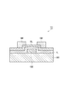
以下、上述した実施形態の方法により形成される有機電極を備え得る有機トランジスタについて説明する。図4〜図7は、上述した実施形態の方法により形成される有機電極を備え得る有機トランジスタを示す断面図である。図4〜図7に示す有機トランジスタは、電界効果トランジスタであり、それぞれ、ボトムゲート・ボトムコンタクト型、ボトムゲート・トップコンタクト型、トップゲート・ボトムコンタクト型、トップゲート・トップコンタクト型の有機トランジスタである。図4〜図7に示す有機トランジスタT1〜T4は各々、ベース基板BS、ゲート電極GE、ソース電極SE、ドレイン電極DE、絶縁体層IL、及び、半導体層SLを備えている。 Hereinafter, an organic transistor that can include an organic electrode formed by the method of the above-described embodiment will be described. 4-7 is sectional drawing which shows the organic transistor which may be equipped with the organic electrode formed by the method of embodiment mentioned above. The organic transistors shown in FIGS. 4 to 7 are field effect transistors, which are bottom-gate / bottom-contact, bottom-gate / top-contact, top-gate / bottom-contact, and top-gate / top-contact organic transistors, respectively. is there. Each of the organic transistors T1 to T4 illustrated in FIGS. 4 to 7 includes a base substrate BS, a gate electrode GE, a source electrode SE, a drain electrode DE, an insulator layer IL, and a semiconductor layer SL.
図4に示すボトムゲート・ボトムコンタクト型の有機トランジスタT1では、ゲート電極GEは、ベース基板BSの一主面上に設けられている。絶縁体層ILは、ゲート電極GE及びベース基板BSの一主面を覆うように設けられている。半導体層SLは、ゲート電極の上方において、絶縁体層IL上に設けられている。ソース電極SE及びドレイン電極DEは、それらの間に、ゲート電極GE上の半導体層SLと絶縁体層ILの界面が介在するように、絶縁体層IL上に設けられている。 In the bottom-gate / bottom-contact type organic transistor T1 shown in FIG. 4, the gate electrode GE is provided on one main surface of the base substrate BS. The insulator layer IL is provided so as to cover one main surface of the gate electrode GE and the base substrate BS. The semiconductor layer SL is provided on the insulator layer IL above the gate electrode. The source electrode SE and the drain electrode DE are provided on the insulator layer IL so that an interface between the semiconductor layer SL on the gate electrode GE and the insulator layer IL is interposed therebetween.
図5に示すボトムゲート・トップコンタクト型の有機トランジスタT2では、ゲート電極GEは、ベース基板BSの一主面上に設けられている。絶縁体層ILは、ゲート電極GE及びベース基板BSの一主面を覆うように設けられている。半導体層SLは、絶縁体層IL上に一様に設けられている。ソース電極SE及びドレイン電極DEは、それらの間に、ゲート電極GE上の半導体層SLと絶縁体層ILの界面が介在するように、絶縁体層IL上に設けられている。 In the bottom gate / top contact type organic transistor T2 shown in FIG. 5, the gate electrode GE is provided on one main surface of the base substrate BS. The insulator layer IL is provided so as to cover one main surface of the gate electrode GE and the base substrate BS. The semiconductor layer SL is provided uniformly on the insulator layer IL. The source electrode SE and the drain electrode DE are provided on the insulator layer IL so that an interface between the semiconductor layer SL on the gate electrode GE and the insulator layer IL is interposed therebetween.
図6に示すトップゲート・ボトムコンタクト型の有機トランジスタT3では、半導体層SLは、ベース基板BSの一主面上に設けられている。ソース電極SE及びドレイン電極DEは、それらの間に半導体層SLが介在するように、ベース基板BS上に設けられている。絶縁体層ILは、ソース電極SE、ドレイン電極DE、及び半導体層SLを覆うように設けられている。ゲート電極GEは、ソース電極SEとドレイン電極DEの間に介在する絶縁体層ILと半導体層SLの界面の上方において、絶縁体層IL上に設けられている。 In the top gate / bottom contact type organic transistor T3 shown in FIG. 6, the semiconductor layer SL is provided on one main surface of the base substrate BS. The source electrode SE and the drain electrode DE are provided on the base substrate BS so that the semiconductor layer SL is interposed therebetween. The insulator layer IL is provided so as to cover the source electrode SE, the drain electrode DE, and the semiconductor layer SL. The gate electrode GE is provided on the insulator layer IL above the interface between the insulator layer IL and the semiconductor layer SL interposed between the source electrode SE and the drain electrode DE.
また、図7に示すトップゲート・トップコンタクト型の有機トランジスタT4では、半導体層SLは、ベース基板BSの一主面を覆うように設けられている。ソース電極SE及びドレイン電極DEは、互いに離間するよう、半導体層SL上に設けられている。絶縁体層ILは、ソース電極SE、ドレイン電極DE、及び半導体層SLを覆うように設けられている。ゲート電極GEは、ソース電極SEとドレイン電極DEの間、且つ、絶縁体層ILと半導体層SLの界面の上方において、絶縁体層IL上に設けられている。 In the top gate / top contact type organic transistor T4 shown in FIG. 7, the semiconductor layer SL is provided so as to cover one main surface of the base substrate BS. The source electrode SE and the drain electrode DE are provided on the semiconductor layer SL so as to be separated from each other. The insulator layer IL is provided so as to cover the source electrode SE, the drain electrode DE, and the semiconductor layer SL. The gate electrode GE is provided on the insulator layer IL between the source electrode SE and the drain electrode DE and above the interface between the insulator layer IL and the semiconductor layer SL.
図4〜図7に示す有機トランジスタにおいて、ベース基板BSは、絶縁性の基板であり、例えば、ガラス、石英、単結晶シリコン、多結晶シリコン、アモルファスシリコン、又は、合成樹脂等から構成され得る。合成樹脂としては、ポリエチレンテレフタレート(PET)、ポリエチレンナフタレート、ポリエーテルスルホン、ポリエーテルイミド、ポリエーテルエーテルケトン、ポリフェニレンスルフィド、ポリアリレート、ポリイミド、ボリカーボネート、環状ポリオレフィン等が例示される。 4 to 7, the base substrate BS is an insulating substrate and can be made of, for example, glass, quartz, single crystal silicon, polycrystalline silicon, amorphous silicon, or synthetic resin. Examples of the synthetic resin include polyethylene terephthalate (PET), polyethylene naphthalate, polyethersulfone, polyetherimide, polyetheretherketone, polyphenylene sulfide, polyarylate, polyimide, polycarbonate, and cyclic polyolefin.
また、図4〜図7に示す有機トランジスタにおいて、半導体層SLは、有機半導体層である。有機半導体層を形成するための有機半導体材料としては、所望の半導体特性を備えた材料、例えば、芳香族化合物、鎖式化合物、有機顔料、有機ケイ素化合物等が例示される。より具体的には、有機半導体材料としては、ペンタセン等の低分子有機化合物、ポリピロール類、ポリチオフェン類、ポリイソチアナフテン類、ポリチェニレンビニレン類、ポリ(p−フェニレンビニレン)類、ポリアニリン類、ポリアセチレン類、ポリアズレン類等の高分子有機化合物が例示される。 In the organic transistors shown in FIGS. 4 to 7, the semiconductor layer SL is an organic semiconductor layer. Examples of the organic semiconductor material for forming the organic semiconductor layer include materials having desired semiconductor characteristics, such as aromatic compounds, chain compounds, organic pigments, and organic silicon compounds. More specifically, examples of the organic semiconductor material include low molecular organic compounds such as pentacene, polypyrroles, polythiophenes, polyisothianaphthenes, polychenylene vinylenes, poly (p-phenylene vinylenes), polyanilines, High molecular organic compounds such as polyacetylenes and polyazulenes are exemplified.
図4〜図7に示す有機トランジスタの絶縁体層ILには、有機トランジスタに一般的に用いられる無機絶縁材料又は有機絶縁材料を用いることができる。無機絶縁材料としては、ガラス、酸化ケイ素(SiO2)、窒化ケイ素、窒化アルミニウム等のほか、金属酸化物である酸化アルミニウム、酸化タンタル、酸化チタン、酸化スズ、酸化バナジウム、チタン酸ストロンチウム、チタン酸バリウムストロンチウム、ジルコニウム酸チタン酸バリウム、ジルコニウム酸チタン酸鉛、チタン酸鉛ランタン、チタン酸バリウム、フッ化バリウムマグネシウム、チタン酸ビスマス、チタン酸ストロンチウムビスマス、タンタル酸ストロンチウムビスマス、タンタル酸ニオブ酸ビスマス、トリオキサイドイットリウム、酸化ハフニウム等が例示される。 For the insulator layer IL of the organic transistor shown in FIGS. 4 to 7, an inorganic insulating material or an organic insulating material generally used for the organic transistor can be used. Examples of inorganic insulating materials include glass, silicon oxide (SiO2), silicon nitride, aluminum nitride, and other metal oxides such as aluminum oxide, tantalum oxide, titanium oxide, tin oxide, vanadium oxide, strontium titanate, and barium titanate. Strontium, barium zirconate titanate, lead zirconate titanate, lead lanthanum titanate, barium titanate, magnesium barium fluoride, bismuth titanate, strontium bismuth titanate, strontium bismuth tantalate, bismuth tantalate niobate, trioxide Examples include yttrium and hafnium oxide.
有機絶縁材料としては、例えば、ポリイミド、ポリアミド、ポリエステル、ポリアクリレート、フェノール系樹脂、フッ素系樹脂、エポキシ系樹脂、ノボラック系樹脂、ビニル系樹脂等の高分子材料が例示される。 Examples of the organic insulating material include polymer materials such as polyimide, polyamide, polyester, polyacrylate, phenol resin, fluorine resin, epoxy resin, novolac resin, and vinyl resin.
また、図4〜図7に示す有機トランジスタの各々のゲート電極GE、ソース電極SE、及びドレイン電極DEの全て、又はその一部に、上述した実施形態の方法により形成される有機電極ELを用いることができる。また、図4〜図7に示す有機トランジスタの各々のゲート電極GE、ソース電極SE、及びドレイン電極DEのうち他の一部は、例えば、Ag、Au、Ta、Ti、Al、Zr、Cr、Nb、Hf、Mo、これらの合金、酸化インジウムスズ合金(ITO)、酸化インジウム亜鉛(IZO)等の金属材料、シリコン単結晶、多結晶シリコン、アモルファスシリコン等のシリコン系材料、カーボンブラック、グラファイト等の炭素材料等の導電性材料から構成されていてもよい。 Further, the organic electrode EL formed by the method of the above-described embodiment is used for all or a part of the gate electrode GE, the source electrode SE, and the drain electrode DE of each of the organic transistors shown in FIGS. be able to. In addition, the other part of the gate electrode GE, the source electrode SE, and the drain electrode DE of each of the organic transistors illustrated in FIGS. 4 to 7 includes, for example, Ag, Au, Ta, Ti, Al, Zr, Cr, Nb, Hf, Mo, alloys thereof, metal materials such as indium tin oxide alloy (ITO), indium zinc oxide (IZO), silicon-based materials such as silicon single crystal, polycrystalline silicon, amorphous silicon, carbon black, graphite, etc. You may comprise from electroconductive materials, such as these carbon materials.
図4〜図7の有機トランジスタの各部は、以下に説明するように作成され得る。絶縁体層ILは、無機絶縁材料によって構成される場合には、ドライプロセス又はウェットプロセスにより形成され得る。また、絶縁体層ILは、有機絶縁材料から構成される場合には、ウェットプロセスにより形成され得る。ドライプロセスとしては、例えば、真空蒸着法、分子線エピタキシャル成長法、イオンクラスタービーム法、低エネルギーイオンビーム法、イオンプレーティング法、CVD法、スパッタリング法、大気圧プラズマ法等を用いることができる。また、ウェットプロセスとしては、例えば、スピンコート法、ダイコート法、ロールコート法、バーコート法、LB法、ディップコート法、スプレーコート法、ブレードコート法、キャスト法等の塗布方法や、インクジェット法、スクリーン印刷法、パッド印刷法、フレキソ印刷法、マイクロコンタクトプリンティング法、グラビア印刷法、オフセット印刷法、グラビア・オフセット印刷法等を用いることができる。 Each part of the organic transistor of FIGS. 4 to 7 can be created as described below. The insulator layer IL can be formed by a dry process or a wet process when it is made of an inorganic insulating material. In addition, when the insulator layer IL is made of an organic insulating material, it can be formed by a wet process. As the dry process, for example, a vacuum deposition method, a molecular beam epitaxial growth method, an ion cluster beam method, a low energy ion beam method, an ion plating method, a CVD method, a sputtering method, an atmospheric pressure plasma method, or the like can be used. Examples of the wet process include spin coating methods, die coating methods, roll coating methods, bar coating methods, LB methods, dip coating methods, spray coating methods, blade coating methods, and casting methods, inkjet methods, Screen printing, pad printing, flexographic printing, microcontact printing, gravure printing, offset printing, gravure / offset printing, and the like can be used.
半導体層SLは、ドライプロセス又はウェットプロセスにより形成され得る。ドライプロセスとしては、例えば、真空蒸着法、分子線エピタキシャル成長法、イオンクラスタービーム法、低エネルギーイオンビーム法、イオンプレーティング法、CVD法、スパッタリング法、大気圧プラズマ法等を用いることができる。また、ウェットプロセスとしては、例えば、スピンコート法、ダイコート法、ロールコート法、バーコート法、LB法、ディップコート法、スプレーコート法、ブレードコート法、キャスト法等の塗布方法や、インクジェット法、スクリーン印刷法、パッド印刷法、フレキソ印刷法、マイクロコンタクトプリンティング法、グラビア印刷法、オフセット印刷法、グラビア・オフセット印刷法等を用いることができる。 The semiconductor layer SL can be formed by a dry process or a wet process. As the dry process, for example, a vacuum deposition method, a molecular beam epitaxial growth method, an ion cluster beam method, a low energy ion beam method, an ion plating method, a CVD method, a sputtering method, an atmospheric pressure plasma method, or the like can be used. Examples of the wet process include spin coating methods, die coating methods, roll coating methods, bar coating methods, LB methods, dip coating methods, spray coating methods, blade coating methods, and casting methods, inkjet methods, Screen printing, pad printing, flexographic printing, microcontact printing, gravure printing, offset printing, gravure / offset printing, and the like can be used.
ゲート電極GE、ソース電極SE、及びドレイン電極DEのうち一部又は全ては、上述した実施形態のパターニングされた有機電極を形成する方法により形成され得る。また、ゲート電極GE、ソース電極SE、及びドレイン電極DEのうち他の一部は、下地上に導電性材料を一様に設けた後に、当該導電性材料をフォトリソグラフィー技術によりパターニングすることにより形成してもよく、スクリーン印刷法、インクジェット法、蒸着法等によって導電性材料をパターニングすることにより形成してもよい。 Some or all of the gate electrode GE, the source electrode SE, and the drain electrode DE may be formed by the method for forming the patterned organic electrode of the above-described embodiment. The other part of the gate electrode GE, the source electrode SE, and the drain electrode DE is formed by uniformly providing a conductive material on the base and then patterning the conductive material by a photolithography technique. Alternatively, it may be formed by patterning a conductive material by a screen printing method, an ink jet method, a vapor deposition method or the like.
以下、実施例を挙げて本発明について更に詳しく説明をするが、本発明はこれらの実施例に限定されるものではない。 EXAMPLES Hereinafter, although an Example is given and this invention is demonstrated in more detail, this invention is not limited to these Examples.
(実施例1、及び、比較例1) (Example 1 and Comparative Example 1)
図1に示した方法に従い、ポリエチレンテレフタレート製の基板上にトナーのパターンを形成し、PEDOT及びPSSを含有する溶液を基板上に滴下し、当該溶液を乾燥させた後に、20質量%のポリエチレングリコール及び80質量%のトルエンを含む剥離液によりトナーを剥離することで作成した有機電極を、実施例1とした。実施例1では、トナーのパターンの形成にキャノン社製レーザプリンタ LBP B10を用いた。また、トナーの剥離前の実施例1の有機電極を比較例1とした。また、トルエンのみを含む剥離液を用いた点において実施例1の作成条件とは相違する作成条件の下で製造した有機電極を、比較例2とした。 According to the method shown in FIG. 1, a toner pattern is formed on a polyethylene terephthalate substrate, a solution containing PEDOT and PSS is dropped onto the substrate, and the solution is dried, and then 20% by mass of polyethylene glycol. An organic electrode prepared by peeling off the toner with a peeling solution containing 80% by mass of toluene was defined as Example 1. In Example 1, a Canon laser printer LBP B10 was used to form a toner pattern. Further, the organic electrode of Example 1 before the toner peeling was used as Comparative Example 1. Moreover, the organic electrode manufactured under the production conditions different from the production conditions of Example 1 in the point which used the stripping solution containing only toluene was made into the comparative example 2.
実施例1の有機電極、比較例1の有機電極、また、比較例2の有機電極のそれぞれの組成をXPS(X線光電子分光)で分析した。具体的には、硫黄の2p軌道に着目してXPSの出力データを取得し、取得した出力データに含まれる強度(任意単位)を、波形分離によりPEDOTに起因する強度とPSSに起因する強度とに分離し、PSSに起因する強度の積分値に対するPEDOTに起因する強度の積分値の比を求めた。その結果を、図8に示す。 The compositions of the organic electrode of Example 1, the organic electrode of Comparative Example 1, and the organic electrode of Comparative Example 2 were analyzed by XPS (X-ray photoelectron spectroscopy). Specifically, XPS output data is acquired by paying attention to the 2p orbit of sulfur, and the intensity (arbitrary unit) included in the acquired output data is determined by the waveform separation and the intensity caused by PEDOT and the intensity caused by PSS. The ratio of the integral value of the intensity caused by PEDOT to the integral value of the intensity caused by PSS was determined. The result is shown in FIG.
図8に示すように、トナー剥離前の状態、即ち、比較例1の有機電極のPSSの量に対するPEDOTの量の比に対して、トルエンのみを含む剥離液を用いて作成した比較例2の有機電極では、PSSの量に対するPEDOTの量の比は、低下していた。一方、実施例1の有機電極のPSSの量に対するPEDOTの量の比は、トナー剥離前、即ち、比較例1の有機電極のPSSの量に対するPEDOTの量の比に対して、増加していた。このことから、実施例1の有機電極では、剥離液に曝されたことにより、PEDOTの量に対してPSSの量が相対的に減少していることが確認された。したがって、トナーの剥離液にエチレングリコールを含めることにより、有機電極から選択的にPSSを除去して、有機電極の電気伝導率の劣化を抑制し且つ当該電気伝導率を向上し得ることが確認された。 As shown in FIG. 8, in the state before toner peeling, that is, the ratio of the amount of PEDOT to the amount of PSS of the organic electrode in Comparative Example 1 was compared with Comparative Example 2 prepared using a stripping solution containing only toluene. In the organic electrode, the ratio of the amount of PEDOT to the amount of PSS was decreased. On the other hand, the ratio of the amount of PEDOT to the amount of PSS of the organic electrode of Example 1 was increased with respect to the ratio of the amount of PEDOT to the amount of PSS of the organic electrode of Comparative Example 1 before toner peeling. . From this, it was confirmed that in the organic electrode of Example 1, the amount of PSS was decreased relative to the amount of PEDOT by being exposed to the stripping solution. Therefore, it was confirmed that by including ethylene glycol in the toner stripping solution, PSS can be selectively removed from the organic electrode to suppress deterioration of the electrical conductivity of the organic electrode and improve the electrical conductivity. It was.
(実施例2〜7、及び、比較例3〜10) (Examples 2-7 and Comparative Examples 3-10)
図1に示した方法により、ポリエチレンテレフタレート製の基板上にトナーのパターンを形成し、PEDOT及びPSSを含有する溶液を基板上に滴下し、当該溶液を乾燥させた後に、ポリエチレングリコール及びトルエンを含む剥離液によりトナーを剥離することで作成した有機電極を実施例2〜7とした。実施例2〜7では、剥離液に含まれるエチレングリコールの量を、10質量%〜60質量%の間で10質量%ずつ変化させた。また、トルエンのみを含む剥離液を用いた点において実施例2〜7の作成条件とは相違する作成条件の下で製造した有機電極を、比較例3とした。また、トナーの剥離前の比較例3及び実施例2〜7の有機電極を比較例4〜10とした。これら実施例2〜7及び比較例3〜10では、トナーのパターンの形成にキャノン社製レーザプリンタ LBP B10を用いた。 A toner pattern is formed on a polyethylene terephthalate substrate by the method shown in FIG. 1, a solution containing PEDOT and PSS is dropped on the substrate, and the solution is dried, and then contains polyethylene glycol and toluene. Examples 2 to 7 were organic electrodes prepared by peeling the toner with a peeling solution. In Examples 2 to 7, the amount of ethylene glycol contained in the stripping solution was changed by 10% by mass between 10% by mass and 60% by mass. Moreover, the organic electrode manufactured under the production conditions different from the production conditions of Examples 2-7 in the point which used the stripping solution containing only toluene was made into the comparative example 3. Further, the organic electrodes of Comparative Example 3 and Examples 2 to 7 before toner separation were referred to as Comparative Examples 4 to 10. In Examples 2 to 7 and Comparative Examples 3 to 10, a laser printer LBP B10 manufactured by Canon Inc. was used to form a toner pattern.
実施例2〜7及び比較例4〜10の有機電極のそれぞれの電気伝導率を測定した。また、実施例2〜7及び比較例4〜10の有機電極のそれぞれの厚みを測定した。図9に電気伝導率の測定結果を、図10に有機電極の厚みの測定結果を示す。 The electric conductivity of each of the organic electrodes of Examples 2 to 7 and Comparative Examples 4 to 10 was measured. Moreover, each thickness of the organic electrode of Examples 2-7 and Comparative Examples 4-10 was measured. FIG. 9 shows the measurement result of electrical conductivity, and FIG. 10 shows the measurement result of the thickness of the organic electrode.
図9に示すように、剥離液に含まれるエチレングリコールの濃度が10質量%以上且つ40質量%以下である場合に、有機電極の電気伝導率が、トナー剥離前の有機電極の電気伝導率よりも相当に高くなることが確認された。また、剥離液に含まれるエチレングリコールの濃度が20質量%であるときに、有機電極の電気伝導率が、トナー剥離前の有機電極の電気伝導率の約1.5倍の値を有してピーク値となることが確認された。そして、エチレングリコールの濃度を10質量%から30質量%の間で調整することにより、有機電極の電気伝導率をピーク値に近づけることが可能であることが確認された。 As shown in FIG. 9, when the concentration of ethylene glycol contained in the stripping solution is 10% by mass or more and 40% by mass or less, the electrical conductivity of the organic electrode is higher than the electrical conductivity of the organic electrode before toner peeling. Was also confirmed to be considerably higher. Further, when the concentration of ethylene glycol contained in the stripping solution is 20% by mass, the electrical conductivity of the organic electrode has a value about 1.5 times the electrical conductivity of the organic electrode before toner stripping. The peak value was confirmed. It was confirmed that the electrical conductivity of the organic electrode can be brought close to the peak value by adjusting the concentration of ethylene glycol between 10% by mass and 30% by mass.
また、図10に示すように、トルエン及びエチレングリコールを含む剥離液によりトナーを剥離した実施例の有機電極の厚みは、トナー剥離前、即ち、比較例の有機電極の厚みより、小さくなっていた。この結果は、トルエン及びエチレングリコールを含む剥離液によりトナーを剥離すると、剥離液に曝されることにより、有機電極中のPSSが選択的に除去されたことによるものと推測される。 Further, as shown in FIG. 10, the thickness of the organic electrode of the example in which the toner was peeled off with the peeling solution containing toluene and ethylene glycol was smaller than that of the organic electrode of the comparative example before the toner peeling. . This result is presumed to be due to the PSS in the organic electrode being selectively removed when the toner is peeled off with a stripping solution containing toluene and ethylene glycol and exposed to the stripping solution.
10…基板、12…トナー、14…溶液、EL…有機電極、T1,T2,T3,T4…有機トランジスタ、BS…ベース基板、SE…ソース電極、DE…ドレイン電極、GE…ゲート電極、IL…絶縁体層、SL…半導体層。
DESCRIPTION OF
Claims (4)
レーザプリンタにより、基板上にトナーのパターンを形成する工程と、
PEDOT及びPSSを含有する溶液を前記基板上に供給する工程と、
前記トナーを、前記トナー除去用の第1溶媒及び前記PSSを選択的に除去する第2溶媒を含有する剥離液により剥離する工程と、
を含む方法。 A method of forming a patterned organic electrode, comprising:
Forming a toner pattern on a substrate by a laser printer;
Supplying a solution containing PEDOT and PSS onto the substrate;
Removing the toner with a remover containing a first solvent for removing the toner and a second solvent for selectively removing the PSS;
Including methods.
Priority Applications (2)
| Application Number | Priority Date | Filing Date | Title |
|---|---|---|---|
| JP2012201989A JP2014056999A (en) | 2012-09-13 | 2012-09-13 | Method for forming patterned organic electrode |
| US14/026,796 US20140070197A1 (en) | 2012-09-13 | 2013-09-13 | Method for forming patterned organic electrode |
Applications Claiming Priority (1)
| Application Number | Priority Date | Filing Date | Title |
|---|---|---|---|
| JP2012201989A JP2014056999A (en) | 2012-09-13 | 2012-09-13 | Method for forming patterned organic electrode |
Publications (1)
| Publication Number | Publication Date |
|---|---|
| JP2014056999A true JP2014056999A (en) | 2014-03-27 |
Family
ID=50232330
Family Applications (1)
| Application Number | Title | Priority Date | Filing Date |
|---|---|---|---|
| JP2012201989A Pending JP2014056999A (en) | 2012-09-13 | 2012-09-13 | Method for forming patterned organic electrode |
Country Status (2)
| Country | Link |
|---|---|
| US (1) | US20140070197A1 (en) |
| JP (1) | JP2014056999A (en) |
Families Citing this family (1)
| Publication number | Priority date | Publication date | Assignee | Title |
|---|---|---|---|---|
| US10676809B2 (en) | 2018-06-20 | 2020-06-09 | Lockheed Martin Corporation | Methods and systems for generating patterns on flexible substrates |
Family Cites Families (4)
| Publication number | Priority date | Publication date | Assignee | Title |
|---|---|---|---|---|
| TWI258317B (en) * | 2002-01-25 | 2006-07-11 | Semiconductor Energy Lab | A display device and method for manufacturing thereof |
| US20120268338A1 (en) * | 2006-09-25 | 2012-10-25 | Seunghyup Yoo | Conducting polymer antenna |
| US8173046B2 (en) * | 2007-06-18 | 2012-05-08 | Hideo Yoshido | Method of producing a conductive polymer film |
| WO2010119503A1 (en) * | 2009-04-14 | 2010-10-21 | 富士電機ホールディングス株式会社 | Organic electroluminescent element and manufacturing method thereof |
-
2012
- 2012-09-13 JP JP2012201989A patent/JP2014056999A/en active Pending
-
2013
- 2013-09-13 US US14/026,796 patent/US20140070197A1/en not_active Abandoned
Also Published As
| Publication number | Publication date |
|---|---|
| US20140070197A1 (en) | 2014-03-13 |
Similar Documents
| Publication | Publication Date | Title |
|---|---|---|
| US10312375B2 (en) | Thin-film transistor, method for producing thin-film transistor and image display apparatus using thin-film transistor | |
| TWI544629B (en) | Method of forming a semiconductor device | |
| US20100264408A1 (en) | Organic Thin Film Transistors, Active Matrix Organic Optical Devices and Methods of Making the Same | |
| JP2010153794A (en) | Manufacturing method of active channel region utilizing improved drop cast print, and device provided with the same active channel region | |
| JP6887806B2 (en) | Thin film transistor and its manufacturing method | |
| JP5833439B2 (en) | Field effect transistor, manufacturing method thereof, and electronic device using the same | |
| CN102867915A (en) | Semiconductor device and method of manufacturing the same, and method of manufacturing image display device | |
| WO2008093854A1 (en) | Thin film semiconductor device fabrication method and thin film semiconductor device | |
| WO2013011257A1 (en) | Method of forming a top gate transistor | |
| JP2014056999A (en) | Method for forming patterned organic electrode | |
| JP5810650B2 (en) | Organic semiconductor device manufacturing method and organic semiconductor device | |
| Kim et al. | Low-leakage polymeric thin-film transistors fabricated by laser assisted lift-off technique | |
| JP5659567B2 (en) | Organic transistor and method for manufacturing organic transistor | |
| JP5630364B2 (en) | Organic semiconductor device manufacturing method and organic semiconductor device | |
| JP7672648B2 (en) | Inorganic/organic hybrid complementary semiconductor device and method for manufacturing same | |
| JP5757142B2 (en) | Method for manufacturing organic semiconductor element | |
| JP2011258777A (en) | Method of manufacturing semiconductor element | |
| JP2015185789A (en) | Thin film transistor and manufacturing method thereof | |
| JP2017098489A (en) | Organic semiconductor layer forming solution, organic semiconductor layer, and organic thin film transistor | |
| JP2019096727A (en) | Thin film transistor, manufacturing method of thin film transistor and image display unit | |
| JP2010062241A (en) | Manufacturing method for organic thin film transistor, organic thin film transistor, and display device | |
| JP2018186131A (en) | Electrode pattern, electrode pattern forming method, thin film transistor, thin film transistor manufacturing method, and image display device | |
| WO2012121279A1 (en) | Method of manufacturing organic semiconductor layer, method of manufacturing organic transistor, organic transistor, and display device | |
| JP2011165778A (en) | P-type organic thin film transistor, method of manufacturing the same, and coating solution | |
| JP2017195315A (en) | Thin film transistor |