JP2011170914A - Semiconductor device - Google Patents
Semiconductor device Download PDFInfo
- Publication number
- JP2011170914A JP2011170914A JP2010033196A JP2010033196A JP2011170914A JP 2011170914 A JP2011170914 A JP 2011170914A JP 2010033196 A JP2010033196 A JP 2010033196A JP 2010033196 A JP2010033196 A JP 2010033196A JP 2011170914 A JP2011170914 A JP 2011170914A
- Authority
- JP
- Japan
- Prior art keywords
- chip
- signal
- product
- package
- circuit
- Prior art date
- Legal status (The legal status is an assumption and is not a legal conclusion. Google has not performed a legal analysis and makes no representation as to the accuracy of the status listed.)
- Withdrawn
Links
Images


Classifications
-
- G—PHYSICS
- G11—INFORMATION STORAGE
- G11C—STATIC STORES
- G11C7/00—Arrangements for writing information into, or reading information out from, a digital store
- G11C7/10—Input/output [I/O] data interface arrangements, e.g. I/O data control circuits, I/O data buffers
- G11C7/1015—Read-write modes for single port memories, i.e. having either a random port or a serial port
- G11C7/1045—Read-write mode select circuits
-
- G—PHYSICS
- G11—INFORMATION STORAGE
- G11C—STATIC STORES
- G11C5/00—Details of stores covered by group G11C11/00
- G11C5/06—Arrangements for interconnecting storage elements electrically, e.g. by wiring
- G11C5/066—Means for reducing external access-lines for a semiconductor memory clip, e.g. by multiplexing at least address and data signals
-
- G—PHYSICS
- G11—INFORMATION STORAGE
- G11C—STATIC STORES
- G11C2207/00—Indexing scheme relating to arrangements for writing information into, or reading information out from, a digital store
- G11C2207/10—Aspects relating to interfaces of memory device to external buses
- G11C2207/105—Aspects related to pads, pins or terminals
-
- H—ELECTRICITY
- H10—SEMICONDUCTOR DEVICES; ELECTRIC SOLID-STATE DEVICES NOT OTHERWISE PROVIDED FOR
- H10W—GENERIC PACKAGES, INTERCONNECTIONS, CONNECTORS OR OTHER CONSTRUCTIONAL DETAILS OF DEVICES COVERED BY CLASS H10
- H10W20/00—Interconnections in chips, wafers or substrates
- H10W20/40—Interconnections external to wafers or substrates, e.g. back-end-of-line [BEOL] metallisations or vias connecting to gate electrodes
- H10W20/49—Adaptable interconnections, e.g. fuses or antifuses
- H10W20/491—Antifuses, i.e. interconnections changeable from non-conductive to conductive
-
- H—ELECTRICITY
- H10—SEMICONDUCTOR DEVICES; ELECTRIC SOLID-STATE DEVICES NOT OTHERWISE PROVIDED FOR
- H10W—GENERIC PACKAGES, INTERCONNECTIONS, CONNECTORS OR OTHER CONSTRUCTIONAL DETAILS OF DEVICES COVERED BY CLASS H10
- H10W20/00—Interconnections in chips, wafers or substrates
- H10W20/40—Interconnections external to wafers or substrates, e.g. back-end-of-line [BEOL] metallisations or vias connecting to gate electrodes
- H10W20/49—Adaptable interconnections, e.g. fuses or antifuses
- H10W20/493—Fuses, i.e. interconnections changeable from conductive to non-conductive
-
- H—ELECTRICITY
- H10—SEMICONDUCTOR DEVICES; ELECTRIC SOLID-STATE DEVICES NOT OTHERWISE PROVIDED FOR
- H10W—GENERIC PACKAGES, INTERCONNECTIONS, CONNECTORS OR OTHER CONSTRUCTIONAL DETAILS OF DEVICES COVERED BY CLASS H10
- H10W70/00—Package substrates; Interposers; Redistribution layers [RDL]
- H10W70/60—Insulating or insulated package substrates; Interposers; Redistribution layers
- H10W70/62—Insulating or insulated package substrates; Interposers; Redistribution layers characterised by their interconnections
- H10W70/65—Shapes or dispositions of interconnections
-
- H—ELECTRICITY
- H10—SEMICONDUCTOR DEVICES; ELECTRIC SOLID-STATE DEVICES NOT OTHERWISE PROVIDED FOR
- H10W—GENERIC PACKAGES, INTERCONNECTIONS, CONNECTORS OR OTHER CONSTRUCTIONAL DETAILS OF DEVICES COVERED BY CLASS H10
- H10W72/00—Interconnections or connectors in packages
- H10W72/90—Bond pads, in general
- H10W72/941—Dispositions of bond pads
- H10W72/944—Dispositions of multiple bond pads
- H10W72/9445—Top-view layouts, e.g. mirror arrays
-
- H—ELECTRICITY
- H10—SEMICONDUCTOR DEVICES; ELECTRIC SOLID-STATE DEVICES NOT OTHERWISE PROVIDED FOR
- H10W—GENERIC PACKAGES, INTERCONNECTIONS, CONNECTORS OR OTHER CONSTRUCTIONAL DETAILS OF DEVICES COVERED BY CLASS H10
- H10W90/00—Package configurations
- H10W90/701—Package configurations characterised by the relative positions of pads or connectors relative to package parts
- H10W90/751—Package configurations characterised by the relative positions of pads or connectors relative to package parts of bond wires
- H10W90/754—Package configurations characterised by the relative positions of pads or connectors relative to package parts of bond wires between a chip and a stacked insulating package substrate, interposer or RDL
Landscapes
- Dram (AREA)
- Semiconductor Memories (AREA)
Abstract
【課題】単一の半導体メモリチップを互いに異なるピン配列を備えたパッケージに実装する場合に、半導体メモリチップのパッド数の増加を防止する。
【解決手段】製品指定情報が、ボンディンク回路、ヒューズ回路等の製品指定情報回路228から与えられる。デコーダ回路224は、この製品指定情報をデコードして、該デコード結果に応じて複数の信号回路220の1つを選択的にチップ・パッド210に接続する。
【選択図】図10An object of the present invention is to prevent an increase in the number of pads of a semiconductor memory chip when a single semiconductor memory chip is mounted on a package having different pin arrangements.
Product designation information is provided from a product designation information circuit 228 such as a bonding circuit or a fuse circuit. The decoder circuit 224 decodes the product designation information and selectively connects one of the plurality of signal circuits 220 to the chip pad 210 according to the decoding result.
[Selection] Figure 10
Description
本発明は、半導体装置に係り、特に、半導体チップのパッケージ技術に関する。 The present invention relates to a semiconductor device, and more particularly to a semiconductor chip packaging technique.
現在、半導体装置は、高容量化および高速化が進んでいるだけでなく、パッケージのサイズも同時に縮小化されている。DRAM(Dinamic Random Access Memory)は、高機能なメモリとして、携帯電話、サーバ、PC(Personal Computer)等、様々な用途に使用されているため、少品種、且つ、大量生産が求められている。したがって、1つのチップで、4、8、16、32ビット等、異なるデータ幅で動作可能なDRAMチップが開発されている。このようなDRAMチップは、4ビット構成品、8ビット構成品、16ビット構成品、32ビット構成品(以下、×4品、×8品、16品、×32品と記載)のいずれか一つとして使用可能である。また、一般製品は、JEDEC(Joint Electronic Device Engineering Council)と呼ばれる組織により標準化されている。この規格では、DRAMチップおよびデータ幅に応じて、パッケージのピン配置、ピンの信号の割り当て等が定められている。 Currently, semiconductor devices are not only increasing in capacity and speed, but also being reduced in package size. DRAM (Dynamic Random Access Memory) is used for various purposes such as a mobile phone, a server, and a PC (Personal Computer) as a high-performance memory. Accordingly, DRAM chips that can operate with different data widths such as 4, 8, 16, and 32 bits have been developed. Such a DRAM chip is any one of a 4-bit component, an 8-bit component, a 16-bit component, and a 32-bit component (hereinafter referred to as x4 product, x8 product, 16 product, and x32 product). It can be used as one. Further, general products are standardized by an organization called JEDEC (Joint Electronic Device Engineering Council). In this standard, package pin arrangement, pin signal assignment, and the like are determined according to the DRAM chip and data width.
引用文献1では、×16品として動作させる際に、DQ系上位ビット側パッドとして用いられる複数のパッド(パッケージパッド)が配列形成されるパッケージのDQ系上位ビット側パッド領域に、DQ系上位ビット側パッド以外の
追加のパッドを形成させた半導体装置が開示されている。該追加のパッドは、×4品又は×8品として動作させる際に使用される。すなわち、パッドを追加することにより、×4品、×8品および×16品のいずれのビット構成品としても動作可能な半導体装置を得ている。また、引用文献1に示された半導体装置は、DDR3 SDRAMチップとして使用されることが前提となっており、DDR2 SDRAMチップについては何ら記載されていない。パッケージのピン配置およびピンの信号の割り当ては、DDR2 SDRAMチップとDDR3 SDRAMチップでは全く異なるため、DDR2 SDRAMチップでは、DDR3 SDRAMチップとは異なる配慮が必要である。
In
上述のように、半導体メモリチップおよびデータ幅の種類により、パッケージのピン配置およびピンの信号の割り当てが異なる。また、異なるビット構成品を同一のチップで構成するには、専用のチップパッドが必要となるため、チップサイズが増大する。 As described above, the package pin arrangement and pin signal allocation differ depending on the type of semiconductor memory chip and data width. In addition, in order to configure different bit components on the same chip, a dedicated chip pad is required, which increases the chip size.
本発明の一態様によれば、所定数のチップパッドからなるパッド配列を備え、×8品、×16品および×32品のいずれか一つで動作可能な半導体メモリチップと、複数のピンからなるピン配列とを備えたパッケージとを有し、前記チップパッド配列は、少なくとも2列に配列されると共に、前記半導体メモリチップは、所定のチップパッドに接続するピンの信号に応じて、前記所定のチップパッドに接続させる信号回路を、切り替える切り替え回路を備え、前記切り替え回路により、前記パッケージが×8品の場合、前記所定のチップパッドはリードデータストローブ信号用の信号回路に接続され、前記パッケージが×16品の場合、前記所定のチップパッドはデータ信号用の信号回路に接続されることを特徴とする半導体装置が得られる。 According to one aspect of the present invention, a semiconductor memory chip having a pad array composed of a predetermined number of chip pads and operable in any one of x8 products, x16 products, and x32 products, and a plurality of pins The chip pad array is arranged in at least two rows, and the semiconductor memory chip is arranged in accordance with a signal of a pin connected to a predetermined chip pad. A switching circuit for switching a signal circuit to be connected to the chip pad, and when the package is × 8 products, the predetermined chip pad is connected to a signal circuit for a read data strobe signal by the switching circuit, and the package Is a × 16 product, the predetermined chip pad is connected to a signal circuit for data signals, thereby obtaining a semiconductor device.
本発明の別の態様によれば、所定数のチップパッドと、前記チップパッドのうち、特定のチップパッドの信号を切り替える切り替え回路を備え、×8品、×16品および×32品のいずれか一つのDDR2 SDRAMチップとして動作可能であることを特徴とする半導体メモリチップが得られる。 According to another aspect of the present invention, there is provided a predetermined number of chip pads and a switching circuit for switching a signal of a specific chip pad among the chip pads, and any of x8 products, x16 products and x32 products is provided. A semiconductor memory chip can be obtained which can operate as one DDR2 SDRAM chip.
本発明のさらに別の態様によれば、所定数のチップパッドからなるパッド配列を備え、×8品、×16品および×32品のいずれか一つとして動作可能な半導体メモリチップと、複数のピンからなるピン配列とを備えたパッケージとを用意し、前記パッケージが×8品の場合、所定のチップパッドはリードデータストローブ信号用の信号回路に接続され、前記パッケージが×16品の場合、前記所定のチップパッドはデータ信号用の信号回路に接続され、前記パッケージが×32品の場合、前記所定のチップパッドはデータストローブ信号用の信号回路に接続されることにより、×8品、×16品および×32品のDDR2 SDRAMを個別に製造することを特徴とする半導体装置の製造方法が得られる。 According to still another aspect of the present invention, a semiconductor memory chip having a pad array composed of a predetermined number of chip pads and operable as any one of x8 products, x16 products, and x32 products, A package having a pin arrangement of pins, and when the package is x8 product, a predetermined chip pad is connected to a signal circuit for a read data strobe signal, and when the package is x16 product, When the predetermined chip pad is connected to a signal circuit for data signals and the package is x32 products, the predetermined chip pad is connected to a signal circuit for data strobe signals, so that x8 products, x A method for manufacturing a semiconductor device, characterized in that 16 DDR2 SDRAMs and 32 DDR2 SDRAMs are individually manufactured.
本発明によると、×8品、×16品および×32品のいずれか一つで動作可能な半導体メモリチップは、半導体メモリチップのビット構成品に応じて、チップパッドに接続させる信号回路を切り替える。これにより、専用のチップパッドが不要となり、チップサイズの増大を防止することができる。 According to the present invention, a semiconductor memory chip capable of operating in any one of x8 products, x16 products, and x32 products switches a signal circuit to be connected to a chip pad according to the bit configuration product of the semiconductor memory chip. . This eliminates the need for a dedicated chip pad and prevents an increase in chip size.
以下、図面を参照して、本発明の実施の形態について詳細に説明する。 Hereinafter, embodiments of the present invention will be described in detail with reference to the drawings.
本発明の実施の形態に係る半導体装置は、×8品、×16品および×32品のいずれか一つで動作可能な半導体メモリチップと複数のピン110からなるピン配列とを備えたパッケージ100を有する。ここで、半導体メモリチップは、DDR2 SDRAMチップ200であるとする。
A semiconductor device according to an embodiment of the present invention includes a
理解を容易にするために、先ず、DDR2 SDRAMチップ200のパッケージ100について説明する。
In order to facilitate understanding, first, the
図1〜図3に、JEDECにより標準化されたDDR2 SDRAMチップ200における×8品、×16品および×32品のパッケージ100のピン配置が示されている。パッケージ100のピン110の配置および信号は、JEDECにより定められている。尚、図1〜図3に示されたピン110は、ピン110に付された信号を送受する。ここで、各ピン110で送受される信号について説明すると、Aが冒頭に付された信号はアドレス信号群、BAが冒頭に付された信号はバンクアドレス信号群、DQが冒頭に付された信号はデータ信号群、RASBはロウアドレスストローブ信号、CASBはカラムアドレスストローブ信号、DQS、UDQSおよびLDQSはデータストローブ信号群、DQSB、UDQSBおよびLDQSBは反転データストローブ信号群、RDQSはリードデータストローブ信号、RDQSBは反転リードデータストローブ信号である。また、CSはチップセレクト信号、CSBは反転チップセレクト信号、CKEはクロックイネーブル信号、CKはクロック信号、CKBは反転クロック信号、VDDは内部回路の電源信号、VSSは内部回路のグランド信号、VDDQはデータ回路の電源信号、VSSQはデータ回路のグランド信号、VDDLはDDL回路の電源信号、VSSLはDDL回路のグランド信号、VREFは参照電圧信号、DMが付された信号はデータマスク信号群である。WEBはライトイネーブル信号、ODTはオンダイターミネーション信号である。
FIG. 1 to FIG. 3 show pin arrangements of
即ち、アドレス信号群、バンクアドレス信号群、データ信号群、ロウアドレスストローブ信号、カラムアドレスストローブ信号、データストローブ信号群、DQSB、反転データストローブ信号群、リードデータストローブ信号、反転リードデータストローブ信号、チップセレクト信号、反転チップセレクト信号、クロックイネーブル信号、クロック信号、反転クロック信号、内部回路の電源信号、内部回路のグランド信号、データ回路の電源信号、データ回路のグランド信号、DDL回路の電源信号、DDL回路のグランド信号、参照電圧信号、データマスク信号群、ライトイネーブル信号、オンダイターミネーション信号は、互いに異なる機能を有する信号である。 That is, address signal group, bank address signal group, data signal group, row address strobe signal, column address strobe signal, data strobe signal group, DQSB, inverted data strobe signal group, read data strobe signal, inverted read data strobe signal, chip Select signal, inverted chip select signal, clock enable signal, clock signal, inverted clock signal, internal circuit power signal, internal circuit ground signal, data circuit power signal, data circuit ground signal, DDL circuit power signal, DDL The circuit ground signal, reference voltage signal, data mask signal group, write enable signal, and on-die termination signal are signals having different functions.
以下、DDR2 SDRAMチップ200における×8品、×16品および×32品のパッケージ100のピン配置を具体的に説明する。
Hereinafter, the pin arrangement of the
図1に示すように、DDR2 SDRAMチップ200における×8品のパッケージ100は、60個のピン110を備えている。また、パッケージ100は、データ幅が8ビットであることから8本のデータ信号DQ0〜DQ7、1つのデータストローブ信号対(DQS、DQSB)および1つのリードデータストローブ対(RDQS、RDQSB)を備えている。パッケージ100は、縦方向にA〜Lで示され、横方向に1〜9で示された部分領域に区分されている。パッケージ100は、縦横方向の一点鎖線で表したパッケージ100の中心線により、4つのブロック、すなわち、左下(1〜5、A〜F)、左上(1〜5、F〜L)、右下(5〜9、A〜F)、右上(5〜9、F〜L)のブロックに分けられている。(DQS、DQSB)は、右下のブロックに配置され、(RDQS、RDQSB)は、左下のブロックに配置されている。
As shown in FIG. 1, the × 100
図2に示すように、DDR2 SDRAMチップ200における×16品のパッケージ100は、84個のピン110を備えている。また、パッケージ100は、データ幅が16ビットであることから16本のデータ信号DQ0〜DQ15と、2つのデータストローブ信号対(LDQS、LDQSB)および(UDQS、UDQSB)を備えている。パッケージ100は、縦方向にA〜Rで示され、横方向に1〜9で示された部分領域に区分されている。パッケージ100は、縦横方向の一点鎖線で表したパッケージ100の中心線により、4つのブロック、すなわち、左下(1〜5、A〜H)、左上(1〜5、H〜R)、右下(5〜9、A〜H)、右上(5〜9、H〜R)のブロックに分けると、2つのデータストローブ信号対(LDQS、LDQSB)および(UDQS、UDQSB)ともに、右下のブロックに配置されている。
As shown in FIG. 2, the × 100
図3に示すように、DDR2 SDRAMチップ200における×32品のパッケージ100は、128個のピン110を備えている。パッケージ100は、データ幅が32ビットであることから32本のデータ信号DQ0〜DQ31と、4つのデータストローブ信号対(DQS0〜3、DQS0〜3B)を備えている。パッケージ100は、縦方向にA〜Sで示され、横方向に1〜12で示された部分領域に区分されている。パッケージ100は、縦横方向の一点鎖線で表したパッケージ100の中心線により、4つのブロック、左下(1〜5、A〜H)、左上(1〜5、H〜S)、右下(5〜9、A〜H)、右上(5〜9、H〜S)のブロックに分けると、4つのデータストローブ信号対(DQS0〜3、DQS0〜3B)は、4つのブロックに別々に配置されている。
As shown in FIG. 3, the × 100
上記のように、×8品のパッケージ100は、×16品および×32品のいずれのパッケージ100にもない1つのリードデータストローブ信号対(RDQS、RDQSB)を有し、これらはリードデータストローブ信号用の信号である。データ信号(DQ0〜7)をDDR2 SDRAMチップ200から読み出すとき、すなわち、DDR2 SDRAMチップ200がデータ信号をメモリチップコントローラに出力するときに機能し、データ信号をDDR2 SDRAMチップ200に書き込むときには機能しない。
As described above, the
一方、×8品のパッケージ100における1つのデータストローブ信号対(DQS、DQSB)と、×16品のパッケージ100における2つのデータストローブ信号対(LDQS、LDQSB)、(UDQS、UDQSB)と、×32品のパッケージ100における4つのデータストローブ信号対(DQS0〜3、DQS0〜3B)は、データストローブ信号用の信号であり、DDR2 SDRAMチップ200の読み書きの両方において機能する。
On the other hand, one data strobe signal pair (DQS, DQSB) in the
具体的には、×8品のパッケージ100における1つのデータストローブ信号対(DQS、DQSB)は、DQ0〜7の読み書きのときに機能する。また、×16品のパッケージ100における2つのデータストローブ信号対(LDQS、LDQSB)、(UDQS、UDQSB)は、それぞれDQ0〜7、DQ8〜15の読み書きのときに機能する。×32品のパッケージ100では、4つのデータストローブ信号対(DQS0、DQSB0)、(DQS1、DQSB1)、(DQS2、DQSB2)、(DQS3、DQSB3)は、それぞれDQ0〜7、DQ8〜15、DQ16〜23、DQ24〜31の読み書きのときに機能する。
Specifically, one data strobe signal pair (DQS, DQSB) in the × 8
次に、DDR2 SDRAMチップ200におけるチップパッド210の配置について説明する。
Next, the arrangement of the
図4に示されたDDR2 SDRAMチップ200のチップパッド210は、DDR2 SDRAMチップ200の略中央部分に2列に配置されている。このように、1列よりも2列に配置するほうが、チップの面積を減少させることができるため、本実施の形態では、チップパッド210を2列に配列した場合を例にとって説明する。また、DDR2 SDRAMチップ200は、133個のチップパッド210を有している。
The
ここで、DDR2 SDRAMチップ200における×8品、×16品および×32品のチップパッド210への信号の割り当てについて説明する。
Here, allocation of signals to the
図5を参照すると、チップパッド210の個数は133個であるのに対し、ピン110の個数は、最も多いビット構成品である×32品においても128個であり、チップパッド210の個数のほうが、ピン110の個数より多くなっている。これは、DDR2 SDRAMチップ200には、パッケージ100のピン110には接続されないがテスト動作等のためのチップパッド210が必要であるためである。マイナス記号は不使用又はテスト用、NCは不使用を表す。
Referring to FIG. 5, the number of
次に、パッケージ100に搭載されたチップパッド210について具体的に説明する。
Next, the
図6は、DDR2 SDRAMチップ200における×8品のピン110とチップパッド210間の配線図である。パッケージ100の表面(紙面裏側)には、DDR2 SDRAMチップ200が搭載されている。DDR2 SDRAMチップ200の所定数のチップパッド210からなるチップパッド配列は、パッケージ100の裏面(紙面前側)に向けて、パッケージ100の開口部(図示せず)に配置されている。該開口部を通して、パッケージ100のピン110とDDR2 SDRAMチップ200のチップパッド210が接続される。尚、開口部は、パッケージ100における数字4〜6で示された領域の一部が切り取られることにより形成される。
FIG. 6 is a wiring diagram between the
続いて、パッケージ100のピン110とDDR2 SDRAMチップ200のチップパッド210の接続方法について詳細に説明する。図6に示すように、パッケージ100の裏面には、外部との接続端子となるピン110と、ボンディングフィンガ(図示せず)と、配線120とを備えている。ボンディングフィンガは、チップパッド210とピン110の間に配置される。配線120により、ピン110とボンディングフィンガとが接続される。さらに、ボンディングフィンガと、DDR2 SDRAMチップ200のチップパッド210とが配線120により接続される。このようにパッケージ100のピン110とDDR2 SDRAMチップ200のチップパッド210とが接続された後、配線120を含む開口部を樹脂等で封止することで半導体装置が形成される。
Next, a method for connecting the
図6に示された×8品のパッケージ100における部分領域(3、B)のRDQS信号のピン110は、番号53のチップパッド210に、部分領域(2、A)のRDQSB信号のピン110は、番号54のチップパッド210に接続されている。
The
図7は、DDR2 SDRAMチップ200における×16品の、パッケージ100のピン110とチップパッド210間の配線図である。図示されているように、部分領域(F,1)のDQ6信号のピン110は、番号53のチップパッド210に、部分領域(D,1)のDQ12信号のピン110は、番号54のチップパッド210に接続されている。
FIG. 7 is a wiring diagram between the
図8は、DDR2 SDRAMチップ200における×32品の、パッケージ100のピン110とチップパッド210間の配線図である。図示されているように、部分領域(D,3)のDQS0信号のピン110は、番号53のチップパッド210に、部分領域(C,4)のDQS0B信号のピン110は、番号54のチップパッド210に接続されている。
FIG. 8 is a wiring diagram between the
上記したように、本発明に係る実施形態では、DDR2 SDRAMチップ200では、番号53および54で示されたチップパッド210に割り当てられる信号が×8品、×16品、および、×32品で異なる。しかし、特定のチップパッド210(ここでは、番号53、54)に対して、×8品、×16品、および×32品に応じた信号を切り替える切り替え回路を設けている。
As described above, in the embodiment according to the present invention, in the
ここで、図5に戻ると、図5の点線で囲まれた領域からも理解できるように、番号53のチップパッド210は、×8品の場合はRDQS信号に、×16品の場合はDQ6信号に、×32品の場合はDQS0信号に割り当てられている。同様に、番号54のチップパッド210は、×8品の場合はRDQSB信号に、×16品の場合はDQ12信号に、×32品の場合はDQS0B信号に割り当てられている。即ち、本発明の一実施形態は、番号53および/又は54のチップパッド210の信号の割り当てを切り替えることを特徴としている。後述するが、本発明に係るDDR2 SDRAMチップ200は、チップパッド210に接続する信号回路を切り替える切り替え回路を有することによって特徴付けられる。
Here, referring back to FIG. 5, as can be understood from the region surrounded by the dotted line in FIG. 5, the
これにより、×8品、×16品および×32品を同一のチップで構成する際、×16品および×32品になく、×8品にのみ有するRDQS信号およびRDQSB信号のための専用のチップパッド210を別途設ける必要がなくなり、チップパッド210の増加によるチップサイズの増大を防止することができる。
As a result, when the x8 product, the x16 product and the x32 product are configured with the same chip, the dedicated chip for the RDQS signal and the RDQSB signal which only the x8 product does not have in the x16 product and the x32 product It is not necessary to provide the
図5に示すようにチップパッド210の信号の割り当てを定めた場合、上記以外のチップパッド210のうち切り替えが必要なチップパッド210として、例えば、番号38、39、51、60、94、96、98〜100、111、117、119、120、126のチップパッド210を挙げることができる。例えば、番号120のチップパッド210については、×16品の場合はDQ13信号、×32品の場合はDQS1B信号に切り替える必要がある。×8品の場合は不使用であるため、DQ13信号、DQS1B信号のどちらに接続されても、開放していてもよい。
When the signal allocation of the
その他の番号のチップパッド210については、異なるビット構成品間で同一機能の信号となるように割り当てているため、切り替えは必要ない。例えば、番号92のチップパッド210は、×8品の場合はA11信号、×16品の場合はA11信号、×32品の場合はA4信号の割り当てであるため、切り替えが必要ない。
Since the other numbered
上記のように、×8品〜×32品間で、チップパッド210に同一の機能を有する信号回路を割り当てることにより、異なる機能を有する信号回路同士の切り替えを行う切り替え回路の数を少なくしている。これにより、余分なチップパッド210、切り替え回路、信号回路を省略することができる。
As described above, by assigning signal circuits having the same function to the
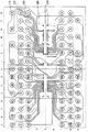
図9および図10に、ビット構成品に応じて、チップパッド210に接続させる信号回路220を、切り替える切り替え回路の実施例を示す。
9 and 10 show an embodiment of a switching circuit for switching the
図9を参照すると、切り替え回路として、ヒューズ222を含むヒューズ回路を用いた例が示されている。図9に示された例では、×8品、×16品および×32品の信号回路220(8)、220(16)および220(32)は、それぞれヒューズ222(8)、222(16)および222(32)を介して、番号54のチップパッド210に設けられている。
Referring to FIG. 9, an example using a fuse circuit including a
図示されたヒューズ222の選択的な切断により、番号54のチップパッド210と信号回路220の接続を切り替える。実線は接続状態、点線は開放状態を示す。この例の場合、番号54のチップパッド210と、×16品および×32品のヒューズの両方が切断されており、×8品のヒューズは接続した状態である。図9に示された切り替え回路は、DDR2 SDRAMチップ200の製造の際は、番号54のチップパッド210に、×8品、×16品および×32品の信号回路220の全てを接続した状態で製造される。組み立て工程の際に、上記のように、ビット構成品に応じてヒューズ222を選択的に切断する。また、ボンディングによって切り替えを行う場合、切り替え回路として、ヒューズ222の代わりにアンチヒューズを含むボンディング回路を用いれば良い。この場合は、DDR2 SDRAMチップ200の製造のときは、×8品、×16品および×32品の信号回路220(8)、220(16)および220(32)と番号54のチップパッド210を、アンチヒューズを介することにより開放しておき、組み立て工程でアンチヒューズを短絡させる。これによって、ビット構成品に応じた信号回路220のいずれか一つを番号54のチップパッド210に接続させることができる。
By selectively cutting the
図10を参照すると、デコーダ回路224と、デコーダ回路224によって制御されるトライステートバッファ226とを組み合わせた回路が切り替え回路として用いられている。図10に示された例では、×8品、×16品および×32品の信号回路220(8)、220(16)および220(32)が、それぞれトライステートバッファ226(8)、226(16)および226(32)を介して、番号54のチップパッド210に設けられている。各トライステートバッファ226は、番号54のチップパッドと各信号回路220の間を流れる方向において反対向きに向いた2つのトライステートバッファ(以下、サブトライステートバッファと記載)から構成される。更に、図示されたデコーダ回路224には、×8品、×16品および×32品のビット構成品に応じた2ビットの製品指定情報が、ボンディング回路、ヒューズ回路、又は、別の回路等の製品指定情報回路228から与えられる。この例においても、番号54のチップパッド210に設けられた信号回路220を切り替え回路によって切り替える場合が示されている。
Referring to FIG. 10, a circuit in which a
図示されたデコーダ回路224は、製品指定情報回路228から2ビットの製品指定情報が与えられると、当該製品指定情報に応じ、トライステートバッファ226のそれぞれに対して、1ビットの制御信号が供給される。
In the illustrated
トライステートバッファ226の各々は、制御信号が、例えば、論理“1”の場合、2つのサブトライステートバッファで信号が入力から出力へ流れることが可能になることにより、番号54のチップパッド210とトライステートバッファ226に対応する信号回路220の間で双方向に信号を流すことができる。このトライステートバッファ226の各々の状態をハイ/ロウ状態と呼ぶ。他方、制御信号が、論理“0”の場合、トライステートバッファ226の各々は、ハイインピーダンス状態となることにより、番号54のチップパッド210と対応する信号回路220が絶縁される。
Each of the
この構成では、製品指定情報回路228から製品指定情報がデコーダ回路224に与えられると、デコーダ回路224は、製品指定情報に応じ、論理“1”の制御信号を単一のトライステートバッファ(例えば、226(8))に出力し、残りの2つのトライステートバッファ(226(16),226(32))には、論理“0”の制御信号を出力する。この結果、論理“1”の制御信号を受けた単一のトライステートバッファ226(8)のみがハイ/ロウ状態となり、信号が入力から出力へ流れることにより、番号54のチップパッドと信号回路220を双方向に信号を流すことができる。論理“0”の制御信号を受けた他のトライステートバッファ228(16)、226(32)は、ハイインピーダンス状態となり、番号54のチップパッドと信号回路220(8)、220(16)、220(32)が絶縁される。このように、図9の場合と同様に、この構成によっても、ビット構成品に応じた信号回路220のいずれか一つをチップパッド54に接続することができる。
In this configuration, when product designation information is given from the product
尚、トライステートバッファ226の各々は、番号54のチップパッド210とトライステートバッファ226に対応する信号回路220の間で一方向にのみ信号を流す場合には、1つのサブトライステートバッファを省略することができる。
Each of the
図2および図3に戻ると、×16品では、2つのデータストローブ信号対(LDQS、LDQSB)および(UDQS、UDQSB)は、右下のブロックに配置されている。一方、×32品では、4つのデータストローブ信号対(DQS0〜3、DQS0〜3B)は、4つのブロックに別々に配置されている。したがって、×32品と×16品を1チップで実現するには、配線120や配線の引き回しが困難であり、専用のチップパッド210が必要であるという問題があった。
Returning to FIG. 2 and FIG. 3, in the x16 product, two data strobe signal pairs (LDQS, LDQSB) and (UDQS, UDQSB) are arranged in the lower right block. On the other hand, in the x32 product, four data strobe signal pairs (DQS0-3, DQS0-3B) are separately arranged in four blocks. Therefore, in order to realize the x32 product and the x16 product with one chip, there is a problem that it is difficult to route the
本実施形態では、図5に示すように、×8品、×16品および×32品のうち、少なくとも2つで共用されるチップパッド210(例えば、番号117、126、128等)を設け、これらチップパッド210近傍に、ビット構成品に応じた信号回路220を設置すると共に、これらチップパッド210と信号回路220との間に、切り替え回路を設けた構成を備えている。この構成によれば、ビット構成品に応じた信号回路220を切り替え回路により選択的にチップパッド210に接続することにより、前述した実施形態と同様な効果を得ることができる。
In the present embodiment, as shown in FIG. 5, chip pads 210 (for example,
100 パッケージ
110 ピン
120 配線
200 DDR2 SDRAMチップ
210 チップパッド
220 信号回路
220(8) ×8品の信号回路
220(16) ×16品の信号回路
220(32) ×32品の信号回路
222 ヒューズ
222(8) ×8品のヒューズ
222(16) ×16品のヒューズ
222(32) ×32品のヒューズ
224 デコーダ回路
226 トライステートバッファ
226(8) ×8品のトライステートバッファ
226(16) ×16品のトライステートバッファ
226(32) ×32品のトライステートバッファ
228 製品指定情報回路
100
Claims (7)
Priority Applications (2)
| Application Number | Priority Date | Filing Date | Title |
|---|---|---|---|
| JP2010033196A JP2011170914A (en) | 2010-02-18 | 2010-02-18 | Semiconductor device |
| US12/801,151 US8238133B2 (en) | 2010-02-18 | 2010-05-25 | Semiconductor device with a selection circuit selecting a specific pad |
Applications Claiming Priority (1)
| Application Number | Priority Date | Filing Date | Title |
|---|---|---|---|
| JP2010033196A JP2011170914A (en) | 2010-02-18 | 2010-02-18 | Semiconductor device |
Publications (1)
| Publication Number | Publication Date |
|---|---|
| JP2011170914A true JP2011170914A (en) | 2011-09-01 |
Family
ID=44369536
Family Applications (1)
| Application Number | Title | Priority Date | Filing Date |
|---|---|---|---|
| JP2010033196A Withdrawn JP2011170914A (en) | 2010-02-18 | 2010-02-18 | Semiconductor device |
Country Status (2)
| Country | Link |
|---|---|
| US (1) | US8238133B2 (en) |
| JP (1) | JP2011170914A (en) |
Families Citing this family (1)
| Publication number | Priority date | Publication date | Assignee | Title |
|---|---|---|---|---|
| US12033945B2 (en) * | 2020-03-27 | 2024-07-09 | Micron Technology, Inc. | Microelectronic device interface configurations, and associated methods, devices, and systems |
Family Cites Families (5)
| Publication number | Priority date | Publication date | Assignee | Title |
|---|---|---|---|---|
| JP3083547B2 (en) * | 1990-07-12 | 2000-09-04 | 株式会社日立製作所 | Semiconductor integrated circuit device |
| TW231343B (en) * | 1992-03-17 | 1994-10-01 | Hitachi Seisakusyo Kk | |
| JP2006278805A (en) * | 2005-03-30 | 2006-10-12 | Elpida Memory Inc | Semiconductor device |
| JP2007095911A (en) | 2005-09-28 | 2007-04-12 | Elpida Memory Inc | Semiconductor device |
| WO2008076790A2 (en) * | 2006-12-14 | 2008-06-26 | Rambus Inc. | Multi-die memory device |
-
2010
- 2010-02-18 JP JP2010033196A patent/JP2011170914A/en not_active Withdrawn
- 2010-05-25 US US12/801,151 patent/US8238133B2/en active Active
Also Published As
| Publication number | Publication date |
|---|---|
| US20110199803A1 (en) | 2011-08-18 |
| US8238133B2 (en) | 2012-08-07 |
Similar Documents
| Publication | Publication Date | Title |
|---|---|---|
| KR100485547B1 (en) | Semiconductor memory device adaptable to various types of packages | |
| US8637998B2 (en) | Semiconductor chip and semiconductor device | |
| US10014037B2 (en) | Semiconductor memory package including memory device with inverting circuit | |
| JP5559507B2 (en) | Semiconductor device and information processing system including the same | |
| JP5490482B2 (en) | Semiconductor device | |
| JP4309368B2 (en) | Semiconductor memory device | |
| JP2011082449A (en) | Semiconductor device | |
| WO2018084909A1 (en) | Wiring with external terminal | |
| JP5635924B2 (en) | Semiconductor device and test method thereof | |
| US10156893B1 (en) | Wiring with external terminal | |
| JP2013114416A (en) | Memory module | |
| US11475940B2 (en) | Semiconductor device layout for a plurality of pads and a plurality of data queue circuits | |
| US7956470B2 (en) | Semiconductor device | |
| JP2011170914A (en) | Semiconductor device | |
| JP2010123203A (en) | Semiconductor device and module device | |
| JP2014096197A (en) | Semiconductor device and testing method thereof | |
| US9226398B1 (en) | Printed circuit board and package substrate having additional conductive pathway space | |
| KR100476393B1 (en) | Semiconductor memory device for reducing package test time | |
| CN115966224B (en) | Multi-die package | |
| JP2011082451A (en) | Package substrate for semiconductor and semiconductor device equipped with the same | |
| KR100306967B1 (en) | Arrangement of data input/output circuits for use in a semiconductor memory integrated circuit device | |
| JP2006024663A (en) | Semiconductor device and semiconductor chip | |
| WO2025084440A1 (en) | Semiconductor device and semiconductor chip | |
| WO2014115599A1 (en) | Semiconductor device | |
| JP2006140466A (en) | Semiconductor memory device |
Legal Events
| Date | Code | Title | Description |
|---|---|---|---|
| A300 | Application deemed to be withdrawn because no request for examination was validly filed |
Free format text: JAPANESE INTERMEDIATE CODE: A300 Effective date: 20130507 |