JP2007287346A - Organic EL display device and method of manufacturing organic EL display device - Google Patents
Organic EL display device and method of manufacturing organic EL display device Download PDFInfo
- Publication number
- JP2007287346A JP2007287346A JP2006109976A JP2006109976A JP2007287346A JP 2007287346 A JP2007287346 A JP 2007287346A JP 2006109976 A JP2006109976 A JP 2006109976A JP 2006109976 A JP2006109976 A JP 2006109976A JP 2007287346 A JP2007287346 A JP 2007287346A
- Authority
- JP
- Japan
- Prior art keywords
- organic
- pixel
- insulating film
- separation partition
- forming
- Prior art date
- Legal status (The legal status is an assumption and is not a legal conclusion. Google has not performed a legal analysis and makes no representation as to the accuracy of the status listed.)
- Granted
Links
Images

Landscapes
- Electroluminescent Light Sources (AREA)
- Devices For Indicating Variable Information By Combining Individual Elements (AREA)
Abstract
【課題】有機EL層の被膜性が安定して、画素電極と対向電極との短絡を抑制した有機EL表示装置を提供する。
【解決手段】有機EL表示装置は、表面に電気回路が形成された基板1と、基板1の上側に形成された層間絶縁膜11とを備える。層間絶縁膜11の上側に形成された画素電極を備える。層間絶縁膜11の上側に形成され、それぞれの画素同士の間に配置された画素分離隔壁21を備える。層間絶縁膜11は、少なくとも一部が画素同士の間に配置されるように形成された窪み部61を有する。画素分離隔壁21は、外縁部が窪み部61の内面の領域に配置されている。
【選択図】図1An organic EL display device in which the film property of an organic EL layer is stable and a short circuit between a pixel electrode and a counter electrode is suppressed is provided.
An organic EL display device includes a substrate having an electric circuit formed on a surface thereof, and an interlayer insulating film formed on the upper side of the substrate. A pixel electrode formed on the upper side of the interlayer insulating film 11 is provided. A pixel isolation partition wall 21 is provided above the interlayer insulating film 11 and disposed between the respective pixels. The interlayer insulating film 11 has a depression 61 formed so that at least a part thereof is disposed between pixels. The pixel separation partition wall 21 is arranged in the region of the inner surface of the recessed portion 61 at the outer edge portion.
[Selection] Figure 1
Description
本発明は、有機EL表示装置および有機EL表示装置の製造方法に関する。 The present invention relates to an organic EL display device and a method for manufacturing the organic EL display device.
有機材料のエレクトロルミネッセンス(Electro Luminescence:略してELと言う)を利用した有機EL素子は、有機正孔輸送層や有機発光層等が積層された有機EL層が陽極と陰極との間に挟まれている構成を含む。有機EL素子は、低電圧の直流駆動による高輝度の発光が可能な発光素子として注目されている。 An organic EL element using electroluminescence (Electro Luminescence: abbreviated as EL) of an organic material has an organic EL layer in which an organic hole transport layer, an organic light emitting layer, etc. are laminated, sandwiched between an anode and a cathode. Including configurations. An organic EL element has attracted attention as a light emitting element capable of emitting light with high luminance by DC driving at a low voltage.
有機EL層を表示素子として用いた表示装置のうち、有機EL素子を駆動するための薄膜トランジスタ(Thin Film Transistor:以下、略してTFTと言う)が画素ごとに形成されたアクティブマトリックス型の表示装置は、基板の表面に形成されたTFTや配線などの電気回路を備える。 Among display devices using an organic EL layer as a display element, an active matrix type display device in which a thin film transistor (hereinafter referred to as TFT for short) for driving the organic EL element is formed for each pixel. An electric circuit such as a TFT or wiring formed on the surface of the substrate is provided.
TFTや配線などの電気回路が形成された基板の上側には、電気回路の表面の凹凸を平坦化するために、少なくとも1層の層間絶縁膜が形成される。この層間絶縁膜は、平坦化絶縁膜とも言われ、電気的な絶縁性を有する。この平坦化絶縁膜としては、たとえば有機膜が形成されている。平坦化絶縁膜の上側には、有機EL素子の陽極となる画素電極が形成される。画素電極の表面には有機EL層が形成される。画素電極は、平坦化絶縁膜に形成されたコンタクトを介してTFTに接続される。 On the upper side of the substrate on which the electric circuit such as TFT and wiring is formed, at least one interlayer insulating film is formed in order to flatten the unevenness on the surface of the electric circuit. This interlayer insulating film is also called a planarization insulating film and has electrical insulation. As this planarization insulating film, for example, an organic film is formed. A pixel electrode serving as an anode of the organic EL element is formed on the planarization insulating film. An organic EL layer is formed on the surface of the pixel electrode. The pixel electrode is connected to the TFT through a contact formed in the planarization insulating film.
有機EL層の上側には、有機EL素子の陰極となる対向電極が形成される。対向電極は、たとえば接地されている。有機EL表示装置は、画素を備えるものがある。有機EL表示装置は、複数の画素が集まることにより、映像や画像などを表示するように形成されている。TFTおよび画素電極は、それぞれの画素ごとに形成され、それぞれの画素を駆動するように形成される。有機EL層は、たとえば、それぞれの画素毎に形成されている。対向電極は、たとえば、複数の画素の有機EL層を覆うように、共通する電極が形成される。 On the upper side of the organic EL layer, a counter electrode serving as a cathode of the organic EL element is formed. The counter electrode is grounded, for example. Some organic EL display devices include pixels. The organic EL display device is formed to display a video, an image, and the like by collecting a plurality of pixels. The TFT and the pixel electrode are formed for each pixel, and are formed so as to drive each pixel. The organic EL layer is formed for each pixel, for example. As the counter electrode, for example, a common electrode is formed so as to cover the organic EL layers of a plurality of pixels.
それぞれの画素は、互いに分離されている。それぞれの画素同士の間には、画素同士を分離するための画素分離隔壁が形成される場合がある。画素分離隔壁は、それぞれの画素を取囲むように形成され、互いに隣り合う画素同士を分離する。 Each pixel is separated from each other. A pixel separation partition for separating the pixels may be formed between the pixels. The pixel separating partition is formed so as to surround each pixel, and separates adjacent pixels.
特許第3691313号公報においては、陽極、発光素子層および陰極を積層して発光領域を形成する表示装置であって、陽極の端部において、陽極と発光素子層および陰極とを離間する平坦化絶縁膜を備える表示装置が開示されている。この表示装置は、平坦化絶縁膜によって陰極の表面が平坦であるとともに、発光素子層は、発光領域および平坦化絶縁膜を覆って設けられており、かつ平坦化絶縁膜の開口部によって発光領域が規定されている。平坦化絶縁膜は、陽極上にその端部を有し、該端部が傾斜を有する。この表示装置によれば、陽極の厚さによる発光素子層の断線に起因して、陰極が陽極と短絡することを防止するとともに、陽極エッジの電界集中による発光層の劣化を抑制できると開示されている。 Japanese Patent No. 3691313 discloses a display device in which a light emitting region is formed by laminating an anode, a light emitting element layer, and a cathode, and planarization insulation that separates the anode from the light emitting element layer and the cathode at the end of the anode. A display device comprising a film is disclosed. In this display device, the surface of the cathode is flat by the planarization insulating film, the light emitting element layer is provided to cover the light emitting region and the planarization insulating film, and the light emitting region is formed by the opening of the planarization insulating film. Is stipulated. The planarization insulating film has an end portion on the anode, and the end portion has an inclination. According to this display device, it is disclosed that the cathode can be prevented from being short-circuited with the anode due to the disconnection of the light emitting element layer due to the thickness of the anode, and the deterioration of the light emitting layer due to the electric field concentration at the anode edge can be suppressed. ing.
特開2002−164181号公報においては、陽極上に絶縁膜を形成し、絶縁膜上にEL膜、陰極を形成したEL素子において、絶縁膜の下端部、上端部を曲面形状とした表示装置が開示されている。また、絶縁膜の中央部のテーパ角を35°以上70°以下とすることが開示されている。この表示装置によれば、EL膜、陰極の断線を防止して、EL膜に局所的に電界が集中することを防ぐことができると開示されている。 Japanese Patent Laid-Open No. 2002-164181 discloses a display device in which an insulating film is formed on an anode, an EL film and a cathode are formed on the insulating film, and the lower end and upper end of the insulating film are curved. It is disclosed. Further, it is disclosed that the taper angle of the central portion of the insulating film is 35 ° or more and 70 ° or less. According to this display device, it is disclosed that disconnection of the EL film and the cathode can be prevented, and an electric field can be prevented from being locally concentrated on the EL film.
特開2001−351787号公報においては、基板上に第1電極、有機LED媒体および第2電極が順次形成され、基板上または第1電極上にテーパ状の隔壁が形成された有機LED素子が開示されている。この有機LED素子においては、隔壁が基板または第1電極の近傍に裾部を有し、裾部の表面が凹面であることが開示されている。この有機LED素子によれば、電極同士の短絡がなく、安価で表示品位の優れたフルカラー表示可能な有機LED素子を提供することができると開示されている。 Japanese Patent Application Laid-Open No. 2001-351787 discloses an organic LED element in which a first electrode, an organic LED medium, and a second electrode are sequentially formed on a substrate, and a tapered partition is formed on the substrate or the first electrode. Has been. In this organic LED element, it is disclosed that the partition has a skirt near the substrate or the first electrode, and the surface of the skirt is concave. According to this organic LED element, it is disclosed that there is no short circuit between electrodes, and an organic LED element capable of full color display which is inexpensive and excellent in display quality can be provided.
特開2003−217855号公報においては、TFTアレイ基板上に平坦化膜が形成され、平坦化膜上には有機EL素子が形成されているエレクトロルミネッセンス表示装置が開示されている。有機EL素子は、陽極である画素電極と画素電極上に形成された発光層と発光層上に形成された陰極とを備えている。画素電極の周部は、絶縁部材で被膜されており、絶縁部材は画素電極の表面との接合先端に向かって厚みが減少するように形成されている。このエレクトロルミネッセンス表示装置によれば、寿命を向上させるとともに製造時の歩留りを向上させることができると開示されている。 Japanese Patent Application Laid-Open No. 2003-217855 discloses an electroluminescence display device in which a planarizing film is formed on a TFT array substrate and an organic EL element is formed on the planarizing film. The organic EL element includes a pixel electrode as an anode, a light emitting layer formed on the pixel electrode, and a cathode formed on the light emitting layer. The peripheral part of the pixel electrode is coated with an insulating member, and the insulating member is formed so that the thickness decreases toward the joint tip with the surface of the pixel electrode. According to this electroluminescence display device, it is disclosed that the lifetime can be improved while the lifetime can be improved.
特開2002−83691号公報においては、TFTによってLED素子の印加電流または印加電圧を制御することができ、画素電極と接続配線とが独立に形成されているアクティブマトリックス駆動型有機LED表示装置が開示されている。また、この公報においては、画素間にテーパ状の絶縁膜を形成することが開示されている。これにより、画素電極のエッジ部での電界集中による素子の劣化を防止することができ、かつ絶縁膜をテーパ状にすることにより、後工程における印刷法による有機LED層を形成した場合にも、印刷機の転写基板が完全に基板に密着するので有機LED層が転写されない部分を生ずることを防止することができると開示されている。 Japanese Patent Application Laid-Open No. 2002-83691 discloses an active matrix driving type organic LED display device in which an applied current or applied voltage of an LED element can be controlled by a TFT, and a pixel electrode and a connection wiring are formed independently. Has been. Further, this publication discloses forming a tapered insulating film between pixels. Thereby, deterioration of the element due to electric field concentration at the edge portion of the pixel electrode can be prevented, and when the organic LED layer is formed by a printing method in a later process by forming the insulating film in a tapered shape, It is disclosed that since the transfer substrate of the printing press is completely in close contact with the substrate, it is possible to prevent a portion where the organic LED layer is not transferred.
特開2001−356711号公報においては、基板上の配線による凹凸を覆う状態で基板上に設けられた層間絶縁膜と、層間絶縁膜上に設けられた有機EL素子とを備えてなる表示装置において、層間絶縁膜は配線を埋込む状態で形成された平坦化絶縁層と、平坦化絶縁層の表面を覆う状態で形成されたコート層とで構成された表示装置が開示されている。この表示装置によれば、平坦化絶縁層とコート層との多層構造からなる層間絶縁膜上に表示素子を設けた構成により、配線による凹凸を有する基板上にあっても、表示素子の表示特性の安定化を図るとともに吸湿による劣化を防止することが可能になると開示されている。
たとえば、上記の特許第3691313号公報、特開2002−164181号公報、特開2001−351787号公報、または特開2003−217855号公報においては、有機EL層や対向電極の被膜性を向上させて、画素電極と対向電極との電気的な短絡、または、有機EL層における電界集中を防止することが図られている。これらの特許文献においては、画素分離隔壁の外縁部の形状や、外縁部の傾斜角度などについては検討されているものの、その角度を得るための方法は製造方法に依存しており、構造上の対策はなされていなかった。 For example, in Japanese Patent No. 3691313, Japanese Patent Application Laid-Open No. 2002-164181, Japanese Patent Application Laid-Open No. 2001-351787, or Japanese Patent Application Laid-Open No. 2003-217855, the coating properties of the organic EL layer and the counter electrode are improved. An attempt is made to prevent electrical short circuit between the pixel electrode and the counter electrode or electric field concentration in the organic EL layer. In these patent documents, although the shape of the outer edge of the pixel separation partition and the inclination angle of the outer edge are studied, the method for obtaining the angle depends on the manufacturing method and is structurally No measures were taken.
従来の技術においては、基板の表面に層間絶縁膜を形成することによって、配線やコンタクトによって生じる表面の凹凸の平坦化を行なう。しかし、TFTなどの電気回路の形成条件や層間絶縁膜の形成条件のばらつきなどに起因して、表面の凹凸が十分に平坦化されていない場合があった。 In the conventional technique, the surface irregularities caused by wiring and contacts are flattened by forming an interlayer insulating film on the surface of the substrate. However, due to variations in the formation conditions of electrical circuits such as TFTs and the formation conditions of interlayer insulating films, surface irregularities may not be sufficiently flattened.
層間絶縁膜の上側に画素電極が形成され、さらに、それぞれの画素同士を区切るための画素分離隔壁が形成される有機EL表示装置においては、基板の電気回路に起因する凹凸やコンタクトに起因する凹凸が、層間絶縁膜の表面に発現する場合がある。 In an organic EL display device in which a pixel electrode is formed on the upper side of the interlayer insulating film and a pixel separation partition for separating each pixel is formed, the unevenness caused by the electrical circuit of the substrate and the unevenness caused by the contact May appear on the surface of the interlayer insulating film.
この凹凸が発現した部分に、画素分離隔壁の外縁部が形成された場合においては、画素分離隔壁の外縁部の傾斜角度が設計値から外れてしまうという問題がある。たとえば、層間絶縁膜の凹凸の凹部に、画素分離隔壁の外縁が配置されている場合には、外縁部が厚くなる。または、層間絶縁膜の凹凸の凸部に、画素分離隔壁の外縁が配置されている場合には、外縁部が薄くなる。この結果、画素分離隔壁の外縁部の傾斜角度が設計値から大きく外れてしまう。たとえば、層間絶縁膜を形成した後の表面の凹凸は、少なくとも0.1μm以上の高低差がある。ここで、層間絶縁膜の表面の凹凸の深さまたは高さが0.1μm変化することにより、画素分離隔壁の外縁部の傾斜角度が、±(10°以上30°以下)の範囲でばらついてしまう。 In the case where the outer edge portion of the pixel separation partition wall is formed in the portion where the unevenness appears, there is a problem that the inclination angle of the outer edge portion of the pixel separation partition wall deviates from the design value. For example, when the outer edge of the pixel separation partition is arranged in the concave and convex portions of the interlayer insulating film, the outer edge becomes thicker. Alternatively, when the outer edge of the pixel separation partition is arranged on the uneven protrusion of the interlayer insulating film, the outer edge becomes thin. As a result, the inclination angle of the outer edge portion of the pixel separation partition is greatly deviated from the design value. For example, the unevenness of the surface after forming the interlayer insulating film has a height difference of at least 0.1 μm or more. Here, when the depth or height of the unevenness on the surface of the interlayer insulating film is changed by 0.1 μm, the inclination angle of the outer edge of the pixel separation partition varies within a range of ± (10 ° to 30 °). End up.
このばらつきは、たとえば特開2001−351787号公報に開示の、60度以下が望ましいとする画素分離隔壁の傾斜角度に対して十分な影響を与えるばらつきである。画素電極の上側および画素分離隔壁の外縁部の上側に形成される有機EL層は、たとえば、約200nmと薄い膜である。画素分離隔壁の外縁部の表面に凹凸が生じることにより、有機EL層の被膜性が悪化して有機EL層が薄くなる場合がある。この結果、画素電極と対向電極とが短絡してしまう場合があるという問題があった。 This variation is, for example, a variation that has a sufficient influence on the inclination angle of the pixel separation partition that is desirably 60 degrees or less, as disclosed in Japanese Patent Application Laid-Open No. 2001-351787. The organic EL layer formed on the upper side of the pixel electrode and the outer edge of the pixel separation partition is a thin film of about 200 nm, for example. When unevenness is generated on the surface of the outer edge of the pixel separation partition wall, the film property of the organic EL layer may deteriorate and the organic EL layer may become thin. As a result, there has been a problem that the pixel electrode and the counter electrode may be short-circuited.
画素電極と対向電極との電気的な短絡を防止する観点から、画素分離隔壁の外縁部においては、傾斜角度の小さな傾斜面を安定的に形成することが好ましい。画素分離隔壁の外縁部の傾斜角度は、画素分離隔壁を形成するための処理を行なう条件に敏感に左右される。安定して画素分離隔壁の外縁部を形成しようとすると、画素分離隔壁を形成するための処理条件が限定的となってしまって製造時の余裕(マージン)が狭くなってしまう。加えて画素分離隔壁を形成する下地の膜に、TFTなどの影響を受けた凹凸やそれに類するうねりが発生することで、通常でも安定に得ることが難しい画素分離隔壁の外縁部の形成をさらに困難にしている問題があった。 From the viewpoint of preventing an electrical short circuit between the pixel electrode and the counter electrode, it is preferable to stably form an inclined surface with a small inclination angle at the outer edge portion of the pixel separation partition wall. The inclination angle of the outer edge of the pixel separation partition is sensitively influenced by the conditions for performing the process for forming the pixel separation partition. If it is attempted to stably form the outer edge of the pixel separation partition, the processing conditions for forming the pixel separation partition are limited, resulting in a narrow manufacturing margin. In addition, it is more difficult to form the outer edge of the pixel separation barrier, which is difficult to obtain normally, because irregularities affected by TFTs or similar undulations occur in the underlying film forming the pixel separation barrier. There was a problem with.
このように、従来の技術においては、画素分離隔壁の外縁部の形状が安定して得られないという問題があった。 As described above, the conventional technique has a problem that the shape of the outer edge portion of the pixel separation partition cannot be stably obtained.
画素分離隔壁の外縁部の下側にTFTや配線などの層間絶縁膜の表面に凹凸が発現する物を配置しないことが考えられる。しかし、たとえば配線は、表示領域内において横方向および縦方向に、画素を跨って形成する必要があるため、画素分離隔壁のすべての外縁部の下側に配線を配置しないことは困難であるという問題がある。TFTにおいても、TFTを配置する領域に制約が生じて、画素の開口率や画素集積率が悪化するという問題があった。 It is conceivable that an object having irregularities on the surface of an interlayer insulating film such as a TFT or a wiring is not disposed below the outer edge of the pixel separation partition. However, for example, since the wiring needs to be formed across the pixels in the horizontal and vertical directions in the display area, it is difficult to dispose the wiring below all the outer edge portions of the pixel separation partition wall. There's a problem. Even in the TFT, there is a problem that the area where the TFT is disposed is restricted, and the aperture ratio and the pixel integration rate of the pixel are deteriorated.
本発明は、有機EL層の被膜性が安定して、画素電極と対向電極との短絡を抑制した有機EL表示装置および有機EL表示装置の製造方法を提供することを目的とする。 An object of the present invention is to provide an organic EL display device in which the film property of an organic EL layer is stable and a short circuit between a pixel electrode and a counter electrode is suppressed, and a method for manufacturing the organic EL display device.
本発明に基づく一の局面における有機EL表示装置は、表面に電気回路が形成された基板を備える。上記基板の上側に形成された絶縁膜を備える。上記絶縁膜の上側に形成され、それぞれの画素ごとに形成された画素電極を備える。上記絶縁膜の上側に形成され、それぞれの上記画素同士の間に配置された画素分離隔壁を備える。上記画素電極の表面に配置された有機EL層を備える。上記有機EL層の表面に形成された対向電極を備える。上記絶縁膜は、少なくとも一部が上記画素同士の間に配置されるように形成された窪み部を有する。上記窪み部は、上記画素に沿って形成されている。上記画素分離隔壁は、外縁部が上記窪み部の内面の領域に配置されている。 The organic EL display device in one aspect based on this invention is equipped with the board | substrate with which the electric circuit was formed in the surface. An insulating film is provided on the upper side of the substrate. A pixel electrode is formed on the insulating film and formed for each pixel. A pixel separation partition is formed on the insulating film and disposed between the pixels. An organic EL layer is provided on the surface of the pixel electrode. A counter electrode is provided on the surface of the organic EL layer. The insulating film has a recess formed so that at least a part thereof is disposed between the pixels. The recess is formed along the pixel. The pixel separation partition has an outer edge arranged in an area on the inner surface of the depression.
本発明に基づく他の局面における有機EL表示装置は、表面に電気回路が形成された基板を備える。上記基板の上側に形成された絶縁膜を備える。上記絶縁膜の上側に形成され、それぞれの画素ごとに形成された画素電極を備える。上記絶縁膜の上側に形成され、それぞれの上記画素同士の間に配置された画素分離隔壁を備える。上記画素電極の表面に形成された有機EL層を備える。上記有機EL層の表面に形成された対向電極を備える。上記絶縁膜は、少なくとも一部が上記画素同士の間に配置されるように形成された隆起部を有する。上記隆起部は、上記画素に沿って形成されている。上記画素分離隔壁は、外縁部が上記隆起部の外面の領域に配置されている。 An organic EL display device according to another aspect of the present invention includes a substrate on which an electric circuit is formed. An insulating film is provided on the upper side of the substrate. A pixel electrode is formed on the insulating film and formed for each pixel. A pixel separation partition is formed on the insulating film and disposed between the pixels. An organic EL layer formed on the surface of the pixel electrode is provided. A counter electrode is provided on the surface of the organic EL layer. The insulating film has a raised portion formed so that at least a part thereof is disposed between the pixels. The raised portion is formed along the pixel. The pixel separation partition wall has an outer edge portion disposed in a region on the outer surface of the raised portion.
本発明に基づく一の局面における有機EL表示装置の製造方法は、基板の表面に電気回路を形成する工程を含む。上記基板の上側に絶縁膜を形成する絶縁膜形成工程を含む。上記絶縁膜の上側において、画素ごとに画素電極を形成する画素電極形成工程を含む。上記絶縁膜の上側の上記画素同士の間に画素分離隔壁を形成する分離隔壁形成工程を含む。上記画素電極の表面に有機EL層を形成する工程を含む。上記有機EL層の表面に対向電極を形成する工程を含む。上記絶縁膜形成工程は、上記画素同士の間の少なくとも一部を含むように、上記画素に沿って窪み部を形成する工程を含む。上記分離隔壁形成工程は、上記窪み部の内面の領域に外縁部が配置されるように上記画素分離隔壁を形成する工程を含む。 The manufacturing method of the organic EL display device in one aspect based on this invention includes the process of forming an electrical circuit on the surface of a board | substrate. An insulating film forming step of forming an insulating film on the upper side of the substrate; A pixel electrode forming step of forming a pixel electrode for each pixel on the upper side of the insulating film is included. A separating partition forming step of forming a pixel separating partition between the pixels on the insulating film. Forming an organic EL layer on the surface of the pixel electrode; Forming a counter electrode on the surface of the organic EL layer; The insulating film forming step includes a step of forming a depression along the pixel so as to include at least a part between the pixels. The separation partition forming step includes a step of forming the pixel separation partition so that an outer edge portion is disposed in a region of the inner surface of the recess.
本発明に基づく他の局面における有機EL表示装置の製造方法は、基板の表面に電気回路を形成する工程を含む。上記基板の上側に絶縁膜を形成する絶縁膜形成工程を含む。上記絶縁膜の上側において、画素ごとに画素電極を形成する画素電極形成工程を含む。上記絶縁膜の上側の上記画素同士の間に画素分離隔壁を形成する分離隔壁形成工程を含む。上記画素電極の表面に有機EL層を形成する工程を含む。上記有機EL層の表面に対向電極を形成する工程を含む。上記絶縁膜形成工程は、上記画素同士の間の少なくとも一部を含むように、上記画素に沿って隆起部を形成する工程を含む。上記分離隔壁形成工程は、上記隆起部の外面の領域に外縁部が配置されるように上記画素分離隔壁を形成する工程を含む。 The manufacturing method of the organic electroluminescence display in the other situation based on this invention includes the process of forming an electrical circuit on the surface of a board | substrate. An insulating film forming step of forming an insulating film on the upper side of the substrate; A pixel electrode forming step of forming a pixel electrode for each pixel on the upper side of the insulating film is included. A separating partition forming step of forming a pixel separating partition between the pixels on the insulating film. Forming an organic EL layer on the surface of the pixel electrode; Forming a counter electrode on the surface of the organic EL layer; The insulating film forming step includes a step of forming a raised portion along the pixel so as to include at least a part between the pixels. The separation partition forming step includes a step of forming the pixel separation partition so that an outer edge portion is disposed in a region of the outer surface of the raised portion.
本発明によれば、有機EL層の被膜性が安定して、画素電極と対向電極との短絡を抑制した有機EL表示装置および有機EL表示装置の製造方法を提供することができる。 ADVANTAGE OF THE INVENTION According to this invention, the coating property of an organic electroluminescent layer is stabilized, and the manufacturing method of the organic electroluminescence display which suppressed the short circuit with a pixel electrode and a counter electrode, and an organic electroluminescence display can be provided.
(実施の形態1)
図1から図16を参照して、本発明に基づく実施の形態1における有機EL表示装置および有機EL表示装置の製造方法について説明する。本実施の形態における有機EL表示装置は、発光した有機EL層の光をTFTが形成された基板と反対側から取出すいわゆるトップエミッション構造の有機EL表示装置である。また、本実施の形態においては、アクティブマトリックス駆動を行なう有機EL表示装置を、例に採り上げて説明する。
(Embodiment 1)
With reference to FIGS. 1 to 16, an organic EL display device and a method for manufacturing the organic EL display device according to the first embodiment of the present invention will be described. The organic EL display device in this embodiment is a so-called top emission structure organic EL display device that takes out light of the emitted organic EL layer from the side opposite to the substrate on which the TFT is formed. In this embodiment, an organic EL display device that performs active matrix driving will be described as an example.
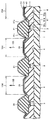
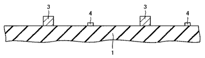
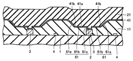
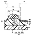
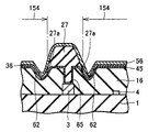
図1は、本実施の形態における第1の有機EL表示装置の一の概略断面図である。図1は、表示面に略垂直な面で切断したときの概略断面図である。本実施の形態における有機EL表示装置は、基板1を備える。基板1は、たとえば、ガラス材料で形成されている。
FIG. 1 is a schematic cross-sectional view of one first organic EL display device in the present embodiment. FIG. 1 is a schematic cross-sectional view taken along a plane substantially perpendicular to the display surface. The organic EL display device in the present embodiment includes a
基板1の表面には、電気回路としてのTFT4が形成されている。また、基板1の表面には、電気回路としての配線3が形成されている。配線3は、TFT4と電気的に接続されている。矢印154に示す領域が、それぞれの画素の領域である。TFT4は、それぞれの画素を個別に駆動するように形成されている。
A
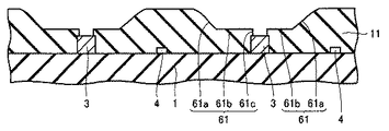
基板1の表面には、絶縁膜としての層間絶縁膜11が形成されている。層間絶縁膜11は、TFT4および配線3などの基板1の表面に形成されている電気回路を覆うように形成されている。本実施の形態における層間絶縁膜11は、有機樹脂で形成されている。層間絶縁膜は、アクリル系樹脂、ポリイミド系樹脂、エポキシ系樹脂などの有機材料のほかに、たとえば、SiO2(酸化シリコン)、PSG,BSG(リンシリカガラス)(ボロンシリカガラス)、SIN4(窒化シリコン系化合物)、Ta2O5(酸化タンタル)などの無機材料を用いることができる。絶縁膜は、この形態に限られず、有機膜と無機膜との積層体、有機膜と有機膜との積層体、または、無機膜と無機膜との積層体であっても構わない。
An interlayer insulating
本実施の形態における層間絶縁膜11は、窪み部61を有する。窪み部61は、層間絶縁膜11の表面から凹むように形成されている。窪み部61は、少なくとも一部が画素同士の間に配置されている。窪み部61は、断面形状がほぼ台形になるように形成されている。窪み部61は、中央部に向かうにつれて、徐々に層間絶縁膜11の厚さが薄くなるように形成されている。窪み部61は、画素を取り囲むように形成されている。窪み部61は、画素に沿って形成されている。
窪み部61は、内面を有する。本実施の形態における窪み部61の内面は、側面61aおよび底面61bを有する。側面61aは、基板1の表面に対して傾斜するように形成されている。側面61aは、基板1に向かって開口が小さくなるようにテーパ状に形成されている。
The
窪み部61は、コンタクトホール61cを有する。コンタクトホール61cは、配線3の表面を層間絶縁膜11の内部から露出するように形成されている。コンタクトホール61cは、底面61bに形成されている。底面61bは、平面状に形成されている。
The
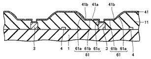
本実施の形態における有機EL表示装置は、層間絶縁膜11の表面に形成された画素電極41を有する。画素電極41は、矢印154に示す画素の領域全体を覆うように形成されている。画素電極41は、不連続部41aを有する。不連続部41aは、それぞれの画素同士の間に配置されている。不連続部41aは、それぞれの画素の画素電極41同士が電気的に不連続になるように形成されている。
The organic EL display device in the present embodiment has a
本実施の形態においては、画素電極41が有機EL素子の陽極になる。画素電極41は、窪み部61の表面に沿って形成されている。画素電極41は、コンタクトホール61cの内面および配線3の表面に形成されている、画素電極41は、配線3と接触することにより、配線3に電気的に導通してコンタクト2が形成されている。
In the present embodiment, the
本実施の形態における有機EL表示装置は、層間絶縁膜11の上側に形成された画素分離隔壁21を有する。画素分離隔壁21は、矢印154に示す画素の領域を取囲むように形成されている。画素分離隔壁21は、突起するように形成されている。画素分離隔壁21は、画素電極41と後述する対向電極51とを引離すように形成されている。本実施の形態における画素分離隔壁21は、層間絶縁膜11の窪み部61の内部に形成されている。画素分離隔壁21は、窪み部61のほぼ中央部に配置されている。
The organic EL display device in the present embodiment has a pixel
画素分離隔壁21は、外縁部を含む。外縁部は、縁21aを有する。外縁部は、窪み部61の内面の領域に配置されるように形成されている。本実施の形態における画素分離隔壁21は、縁21aが側面61aの領域に配置されている。本実施の形態においては、平面視したときに縁21a全体が窪み部61の領域に配置されている。画素分離隔壁21は、外縁部が、縁21aに向かって厚さが徐々に薄くなるように形成されている。すなわち、外縁部は、先端に向かって、徐々に薄くなるように形成されている。
The
本実施の形態における有機EL表示装置は、有機EL層31を含む。本実施の形態における有機EL層31は、矢印154に示す画素の領域を覆うように形成されている。有機EL層31は、画素電極41の表面に形成されている。有機EL層31は、それぞれの画素毎に形成されている。
The organic EL display device in the present embodiment includes an
有機EL層31は、たとえば、正孔注入層、正孔輸送層、電子輸送層および電子注入層を有する。有機EL表示装置がカラー表示を行なう場合には、たとえば、それぞれの画素が赤色、緑色、または青色を発光するように、それぞれの画素に対して異なる有機EL層を形成する。この場合には、3つの画素が1組となってカラー表示を行なうことができる。
The
本実施の形態における有機EL表示装置は、対向電極51を有する。対向電極51は、有機EL層31および画素分離隔壁21の表面に形成されている。本実施の形態における対向電極51は、複数の画素に跨って形成されている。本実施の形態においては、対向電極51が、有機EL素子の陰極になる。
The organic EL display device in the present embodiment has a
有機EL層31は、画素電極41と対向電極51とに挟まれている。それぞれの画素において、TFT4が駆動することにより、配線3を通じて画素電極41に電圧が印加される。この結果、矢印154に示す画素の領域において有機EL層31が発光する。光は、矢印153に示す向きに放出される。
The
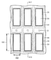
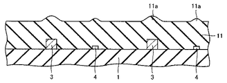
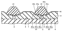
図2に、本実施の形態における有機EL表示装置の他の概略断面図を示す。図2は、表示面にほぼ平行な面で切断したときの概略断面図である。図1は、図2におけるI−I線に関する矢視断面図である。本実施の形態における有機EL表示装置は、複数の画素を有する。矢印151に示す長さおよび矢印152に示す幅を有する領域が1個の画素の領域である。図2においては、6個の画素が記載されている。
FIG. 2 shows another schematic cross-sectional view of the organic EL display device in the present embodiment. FIG. 2 is a schematic cross-sectional view when cut along a plane substantially parallel to the display surface. 1 is a cross-sectional view taken along the line II in FIG. The organic EL display device in the present embodiment has a plurality of pixels. A region having a length indicated by an
それぞれの画素は、平面形状がほぼ長方形になるように形成されている。それぞれの画素は、対向電極51に覆われている。画素電極41、対向電極51および有機EL層31は、それぞれが画素よりも大きくなるように形成されている。
Each pixel is formed so that the planar shape is substantially rectangular. Each pixel is covered with the
有機EL表示装置においては、封止膜や封止基板などの表示装置を封止するために用いられる部材が配置されていても構わない。さらに、封止された内部に、乾燥剤が配置されていても構わない。また、直線偏光板や(1/4)λ板などを組合せた偏光板とそれと同等の光学的機能を有するフィルムが配置されていても構わない。 In the organic EL display device, members used for sealing the display device such as a sealing film and a sealing substrate may be arranged. Furthermore, a desiccant may be disposed inside the sealed interior. Further, a polarizing plate combining a linear polarizing plate, a (1/4) λ plate, and the like and a film having an optical function equivalent to the polarizing plate may be disposed.
ここで、TFT、画素電極、封止部材、または有機EL層などについては、特許第3691313号公報、特開2001−351787号公報または特開2002−83691号公報に開示される公知の材料や製造方法によって形成することができる。また、層間絶縁膜においては、特開2001−356711号公報、特開2002−83691号公報などに開示される公知の材料や製造方法によって形成することができる。 Here, as for TFTs, pixel electrodes, sealing members, organic EL layers, etc., known materials and production disclosed in Japanese Patent No. 3691313, Japanese Patent Laid-Open No. 2001-351787, or Japanese Patent Laid-Open No. 2002-83691 are disclosed. It can be formed by a method. The interlayer insulating film can be formed by known materials and manufacturing methods disclosed in Japanese Patent Application Laid-Open Nos. 2001-356711 and 2002-83691.
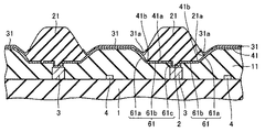
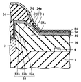
図3に、本実施の形態における第1の有機EL表示装置の画素分離隔壁の部分の拡大概略断面図を示す。本実施の形態における有機EL層31は、端部が画素分離隔壁21の縁21aを含む外縁部に乗り上げるように形成されている。有機EL層31は、曲がり部31aを有する。曲がり部31aは、断面において有機EL層31が曲がるように形成されている。曲がり部31aは、画素分離隔壁21の縁21aの部分に形成されている。対向電極51は、画素分離隔壁21の縁21aの部分に形成された曲がり部51aを有する。
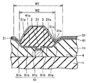
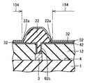
FIG. 3 shows an enlarged schematic cross-sectional view of a pixel separation partition portion of the first organic EL display device in the present embodiment. The
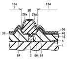
本実施の形態においては、層間絶縁膜11の窪み部61の幅W1は、画素分離隔壁21の幅W2よりも大きくなるように形成されている。窪み部61の幅W1は、製造するときの精度の観点から、画素分離隔壁21の幅W2よりも、0.2μm以上大きくなるように形成されていることが好ましい。
In the present embodiment, the
層間絶縁膜の表面の凹凸およびそれに類するうねりに比べて、桁違いに大きな窪み部を形成することによって、層間絶縁膜の表面の凹凸およびこれに類するうねりを実質的に吸収することができ、画素分離隔壁の外縁部における形状への影響を小さくすることができる。 By forming an indentation that is many orders of magnitude larger than the irregularities on the surface of the interlayer insulating film and the undulations similar thereto, the irregularities on the surface of the interlayer insulating film and the undulations similar thereto can be substantially absorbed. The influence on the shape at the outer edge of the separation partition wall can be reduced.
たとえば、層間絶縁膜の表面の凹凸およびそれに類するうねりの最大高低差の10倍以上の深さを有する窪み部を形成することにより、表面の凹凸を小さくできる。または、たとえば、窪み部を形成しない場合に生じる層間絶縁膜の表面の凹凸およびこれに類するうねりの最大高低差は、層間絶縁膜の厚さの0.1以上5%以下である。層間絶縁膜11においては、窪み部61の底面61bの領域における厚さが、窪み部61が形成されていない部分の厚さの10%以上90%以下が好ましい。
For example, the surface unevenness can be reduced by forming a recess having a depth of 10 times or more the maximum height difference between the surface unevenness of the interlayer insulating film and the swell. Alternatively, for example, the maximum height difference between the unevenness of the surface of the interlayer insulating film and the undulation similar to this when the recess is not formed is 0.1 to 5% of the thickness of the interlayer insulating film. In the
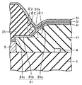
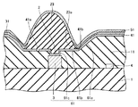
図4に、本実施の形態における第1の有機EL表示装置の画素分離隔壁の外縁部の拡大概略断面図を示す。本実施の形態においては、基板1の表面に対する側面61aの傾斜角度θ1が30°になるように層間絶縁膜11が形成されている。側面61aの傾斜角度θ1は、3°以上80°以下の範囲内で形成されていることが好ましい。
FIG. 4 shows an enlarged schematic cross-sectional view of the outer edge portion of the pixel separation partition of the first organic EL display device in the present embodiment. In the present embodiment,
本実施の形態における画素分離隔壁21は、外縁部の表面が基板1の表面に対して傾斜している。本実施の形態においては、基板1の表面に対する画素分離隔壁21の外縁部の表面の傾斜角度θ2が、50°になるように、画素分離隔壁21が形成されている。画素分離隔壁21の外縁部の表面の傾斜角度θ2は、3°以上60°以下の範囲内で形成することが好ましい。
In the pixel
本実施の形態においては、画素分離隔壁21の外縁部の角度θ3は、傾斜角度θ1と傾斜角度θ2との和である80°になるように形成されている。
In the present embodiment, the angle θ3 of the outer edge portion of the pixel
図5から図11を参照して、本実施の形態における第1の有機EL表示装置の製造方法について説明する。図5から図11は、製造方法のそれぞれの工程を説明する概略断面図である。 With reference to FIG. 5 to FIG. 11, a method for manufacturing the first organic EL display device in the present embodiment will be described. 5 to 11 are schematic cross-sectional views for explaining respective steps of the manufacturing method.
図5に示すように、基板1の表面に、TFT4や配線3などの電気回路を形成する。本実施の形態においては、配線3がTFT4に接続されるように、電気回路を形成する。基板の表面には電気回路の凹凸が生じている。
As shown in FIG. 5, an electric circuit such as
次に、基板の上側に絶縁膜を形成する絶縁膜形成工程を行なう。
図6に示すように、TFT4および配線3などの電気回路全体を覆うように、層間絶縁膜11を形成する。層間絶縁膜11を、スパッタ法、CVD(Chemical Vapor Deposition)法、または塗布法などの公知の方法により形成する。層間絶縁膜は、前述のように無機材料や有機材料を用いることができる。
Next, an insulating film forming step for forming an insulating film on the upper side of the substrate is performed.
As shown in FIG. 6, an
本実施の形態においては、層間絶縁膜11として、感光性を有する公知のアクリル樹脂を用いている。層間絶縁膜11の表面には、電気回路の凹凸に対応して凹凸が発現する。本実施の形態においては、凸部11aが発現する。
In the present embodiment, a known acrylic resin having photosensitivity is used as the
次に、図7に示すように、フォトリソグラフィ法により、層間絶縁膜11に窪み部61を形成する。本実施の形態においては、延びる方向に対して垂直な面で切断したときの断面形状が台形になるように窪み部61を形成する。画素を取り囲むように窪み部61を形成する。画素同士の間の少なくとも一部を含むように窪み部61を形成する。さらに、窪み部61の底面61bにコンタクトホール61cを形成する。コンタクトホール61cを配線3の表面が露出するように形成する。
Next, as shown in FIG. 7, a
基板1の表面に形成された電気回路により、層間絶縁膜11の表面にも凹凸が発現する場合がある。または、層間絶縁膜11には、TFTと配線とを繋ぐコンタクト(図示せず)や、配線と画素電極とを繋ぐコンタクトが形成されている場合がある。これらの電気回路により、層間絶縁膜11の表面にも凹凸が発現する場合がある。しかしながら、層間絶縁膜11に窪み部61を形成することによって、この凹凸の高低差を小さくすることができ、窪み部の内面を平坦化することができる。すなわち、窪み部61の側面61aと底面61bの表面を平坦にすることができる。
Due to the electric circuit formed on the surface of the
本実施の形態においては、ポジ型の感光性樹脂を用いて層間絶縁膜11を形成している。窪み部61の形成においては、窪み部61の領域に他の領域よりも多くの露光を行なう。露光量の多い部分においては、層間絶縁膜の現像量が多くなる。このときに、現像処理が等方的に進行するとはいえ、露光量の増大や現像時間の長時間化等により、表面の凹凸が小さくなる。このように、層間絶縁膜11の表面に発現する凹凸を小さくすることができる。この結果、後の工程にて形成する画素電極の表面に発現する凹凸を小さくすることができる。
In the present embodiment, the
窪み部61の傾斜する側面61aの形成においては、1度のフォトリソグラフィ処理によって形成できるように、フォトマスクを工夫することによって形成することができる。本実施の形態においては、ハーフトーンマスクを用いることにより、基板1の表面にほぼ平行な領域から、連続して傾斜した側面61aを形成できるように露光を行なっている。または、窪み部61が形成される領域において、感光性樹脂に露光を行なう露光条件を制御して露光量を調整することによって、窪み部61を形成することができる。
The
層間絶縁膜の窪み部の形成においては、前述の通り、層間絶縁膜の表面に発現する小さな凹凸に対して十分に深い窪み部を形成することが好ましい。この方法により、表面に発現する小さな凹凸を十分に小さくすることができる。 In the formation of the recess portion of the interlayer insulating film, as described above, it is preferable to form a recess portion that is sufficiently deep with respect to small irregularities that appear on the surface of the interlayer insulating film. By this method, small irregularities appearing on the surface can be made sufficiently small.
次に、層間絶縁膜11に形成されたコンタクトホール61cの内部の配線3の表面に薄く残存する層間絶縁膜11、フォトリソグラフィ法において用いたレジストの残渣物、または、それらの再付着物などの配線3と画素電極41との電気的な接続を阻害する残渣物を除去する。
Next, the
残渣物の除去においては、たとえば、アッシングや清浄化処理を表面全体に対して行なう。アッシングまたは清浄化処理においては、主に公知の有機絶縁物を除去する方法を採用することができる。たとえば、酸素プラズマ処理、紫外線照射オゾン処理、フッ素系プラズマ処理、アルゴンプラズマ処理またはアルカリ溶液処理などを用いることができる。 In removing the residue, for example, ashing or cleaning is performed on the entire surface. In the ashing or cleaning treatment, a known method of removing an organic insulator can be mainly employed. For example, oxygen plasma treatment, ultraviolet irradiation ozone treatment, fluorine plasma treatment, argon plasma treatment, alkaline solution treatment, or the like can be used.
次に、層間絶縁膜の上側に、画素電極を形成する画素電極形成工程を行なう。
図8に示すように、層間絶縁膜11の表面および配線3の表面に、画素電極41を形成する。画素電極41を一様な厚さで形成した後に、画素電極41のパターニングを行なう。
Next, a pixel electrode forming step for forming a pixel electrode is performed on the upper side of the interlayer insulating film.
As shown in FIG. 8, the
本実施の形態においては、クロムを材料として画素電極41を形成している。画素電極41は、たとえば、スパッタ法などで形成することができる。画素電極としては、この形態に限られず、導電性を有する薄膜であれば構わない。たとえば、画素電極41は、金属膜や金属膜の表面に透光性を有する導電膜を積層した膜でも構わない。
In the present embodiment, the
次に、フォトリソグラフィ法により、画素電極41のパターニングを行なう。パターニングにより、画素電極41に不連続部41aを形成する。不連続部41aを形成することにより、それぞれの画素における画素電極41同士が電気的に分離される。
Next, the
次に、絶縁膜の上側に、画素分離隔壁を形成する分離隔壁形成工程を行なう。画素分離隔壁21は、層間絶縁膜11と同様の方法で形成することができる。
Next, a separation partition wall forming step for forming a pixel separation partition is performed on the insulating film. The
図9に示すように、画素電極41の表面にほぼ一様な厚さの画素分離隔壁21を形成する。
As shown in FIG. 9, the pixel
次に、図10に示すように、パターニングを行なって、層間絶縁膜11の窪み部61が形成されている領域に画素分離隔壁21を形成する。パターニングは、公知のフォトリソグラフィ法やエッチング法などにより行なうことができる。画素分離隔壁21を、外側に突出した形状で形成する。外縁部の先端である縁21aに向かって厚さが薄くなるように、画素分離隔壁21を形成する。
Next, as shown in FIG. 10, patterning is performed to form the
本実施の形態においては、画素分離隔壁21の縁21aが、窪み部61の側面61aの領域に配置されるようにパターニングを行なう。画素分離隔壁21の外縁部は、窪み部61の内面の領域に配置される。
In the present embodiment, patterning is performed so that the
画素分離隔壁の形成においては、層間絶縁膜と同様に、有機絶縁膜または無機絶縁膜をそれぞれ単層で形成することができる。または、無機絶縁膜の表面に有機絶縁膜を積層したり、有機絶縁膜の表面に無機絶縁膜を積層したりしても構わない。いずれの積層膜においても、公知のフォトリソグラフィ法やエッチング法などによって形成することができる。 In the formation of the pixel separation partition, each of the organic insulating film and the inorganic insulating film can be formed as a single layer similarly to the interlayer insulating film. Alternatively, an organic insulating film may be stacked on the surface of the inorganic insulating film, or an inorganic insulating film may be stacked on the surface of the organic insulating film. Any laminated film can be formed by a known photolithography method, etching method, or the like.
次に、図11に示すように、有機EL層31を形成する。有機EL層31は、公知の真空蒸着法などにより形成することができる。有機EL層31の形成においては、有機EL層31の端部が画素分離隔壁21の外縁部を覆うように形成する。すなわち、有機EL層31の端部が、画素分離隔壁21の縁21aに乗り上げるように有機EL層31を形成する。有機EL層31には、曲がり部31aが形成される。
Next, as shown in FIG. 11, an
次に、有機EL層31の上側に対向電極を形成する。本実施の形態においては、有機EL層31および画素分離隔壁21を覆うように対向電極を形成することにより、図1に示す有機EL表示装置を製造することができる。
Next, a counter electrode is formed on the upper side of the
本実施の形態においては、絶縁膜形成工程において、少なくとも一部が画素同士の間に配置されるように窪み部を形成する工程を含む。この工程において、層間絶縁膜の表面に発現する凹凸を小さくすることができる。この結果、画素電極の表面に発現する凹凸を画素分離隔壁の外縁部の形状に影響させない程度まで小さくすることができる。 In the present embodiment, the insulating film forming step includes a step of forming the depression so that at least a part is disposed between the pixels. In this step, unevenness appearing on the surface of the interlayer insulating film can be reduced. As a result, the unevenness appearing on the surface of the pixel electrode can be reduced to such an extent that the shape of the outer edge portion of the pixel separation partition is not affected.
たとえば、画素分離隔壁の外縁部の下側に、配線などが横切るように配置されている場合には、画素分離隔壁の外縁部と配線などとが交差する部分で凹凸が生じて、画素分離隔壁の外縁部の角度が大きくなり(外縁部の斜面が急峻になり)、有機EL層の被膜性が悪化する場合がある。この結果、画素電極と対向電極とが短絡して、画素欠陥が生じる場合があった。本発明においては、画素分離隔壁の外縁部の領域における凹凸を小さくすることができ、画素欠陥を抑制することができる。 For example, in the case where wirings and the like are arranged across the outer edge of the pixel separation partition, unevenness occurs at a portion where the outer edge of the pixel separation partition intersects with the wiring, and the pixel separation partition The angle of the outer edge portion becomes larger (the slope of the outer edge portion becomes steeper), and the film property of the organic EL layer may deteriorate. As a result, the pixel electrode and the counter electrode may be short-circuited to cause a pixel defect. In the present invention, unevenness in the region of the outer edge of the pixel separation partition can be reduced, and pixel defects can be suppressed.
本実施の形態における有機EL表示装置においては、画素分離隔壁が、縁に向かって厚さが徐々に薄くなるように形成された外縁部を含む。画素分離隔壁の外縁部が徐々に薄くなると、層間絶縁膜の凹凸の影響が顕著に生じるが、本発明を適用することにより、効果的に画素欠陥を抑制することができる。 In the organic EL display device according to the present embodiment, the pixel separation partition includes an outer edge portion formed so that the thickness gradually decreases toward the edge. When the outer edge of the pixel separation partition wall becomes gradually thinner, the influence of the unevenness of the interlayer insulating film is remarkably generated. However, by applying the present invention, pixel defects can be effectively suppressed.
図12に、本実施の形態における第2の有機EL表示装置の概略断面図を示す。第2の有機EL表示装置は、画素分離隔壁23を有する。画素分離隔壁23は、縁23aを有する外縁部を含む。縁23aは、層間絶縁膜11に形成された窪み部61のうち、側面61aと底面61bとの境界部に配置されている。すなわち、縁23aは、画素電極41の曲がり部41bの部分に配置されるように形成されている。
FIG. 12 is a schematic cross-sectional view of the second organic EL display device in the present embodiment. The second organic EL display device has a
このように、第1の有機EL表示装置においては、画素分離隔壁の縁が層間絶縁膜の窪み部の側面の領域に配置されているが、この形態に限られず、画素分離隔壁の縁が窪み部が形成されている領域であれば同様の作用および効果を得ることができる。たとえば、画素分離隔壁は、縁が窪み部の底面の領域に配置されていても構わない。 As described above, in the first organic EL display device, the edge of the pixel separation partition is disposed in the region of the side surface of the recess portion of the interlayer insulating film. However, the present invention is not limited to this configuration, and the edge of the pixel isolation partition is recessed. Similar operations and effects can be obtained as long as the region is formed with the portion. For example, the pixel separation partition may be arranged in the region of the bottom surface of the recessed portion.
本実施の形態においては、層間絶縁膜の窪み部が平面状の底面を有するように形成されているが、この形態に限られず、窪み部は平面状の底面を有さなくても構わない。たとえば、窪み部の断面形状が円弧状に形成されていても構わない。 In the present embodiment, the recess of the interlayer insulating film is formed to have a planar bottom surface, but the present invention is not limited to this configuration, and the recess may not have a planar bottom surface. For example, the cross-sectional shape of the recess may be formed in an arc shape.
次に、本発明における効果を確認するための試験について説明する。
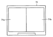
図13に、効果を確認する試験に用いたテストパネルの模式平面図を示す。テストパネル71は、第1領域71aと第2領域71bとを有する。第1領域71aにおいては、本実施の形態における第1の有機EL表示装置を形成する。すなわち、第1領域71aには、層間絶縁膜に窪み部を形成した有機EL表示装置を形成する。第2領域71bには、比較例としての有機EL表示装置を形成する。
Next, the test for confirming the effect in this invention is demonstrated.
FIG. 13 shows a schematic plan view of a test panel used in a test for confirming the effect. The
図14に、比較例としての有機EL表示装置の概略断面図を示す。比較例としての有機EL表示装置は、基板1の表面に形成された層間絶縁膜12を備える。層間絶縁膜12の表面には、窪み部は形成されていない。層間絶縁膜12の表面は、平面状に形成されている。層間絶縁膜12の表面には、画素電極42が形成されている。
FIG. 14 is a schematic cross-sectional view of an organic EL display device as a comparative example. The organic EL display device as a comparative example includes an
画素電極42は、コンタクトホール62cを介して配線3に接続されている。矢印154は画素領域を示す。画素領域同士の間には、画素分離隔壁22が形成されている。画素分離隔壁22の縁22aは、画素電極42の平面状の部分に配置されている。画素電極42の表面には、有機EL層32が配置されている。有機EL層32の端部は、画素分離隔壁22の外縁部に乗り上げている。有機EL層32および画素分離隔壁22の表面には、対向電極52が形成されている。
The
図13を参照して、第1領域71aにおいて本実施の形態における第1の有機EL表示装置を製造して、第2領域71bにおいて比較例の有機EL表示装置を形成することにより、同じ製造処理で比較すべき2種類の有機EL表示装置を製造することができる。また、それぞれの製造工程における処理のばらつきの影響を受けずに、2種類の有機EL表示装置を製造することができる。
Referring to FIG. 13, the same manufacturing process is performed by manufacturing the first organic EL display device according to the present embodiment in the
2種類の有機EL表示装置の比較においては、それぞれの領域に形成した有機EL表示装置の点灯検査を行なって、非点灯の画素の割合を比較した。さらに、製造したテストパネルを長時間連続で動作させることによって、それぞれの有機EL表示装置の信頼性についても確認を行なった。 In the comparison of the two types of organic EL display devices, the lighting test of the organic EL display devices formed in the respective regions was performed, and the ratio of non-lighted pixels was compared. Furthermore, the reliability of each organic EL display device was also confirmed by operating the manufactured test panel continuously for a long time.
図1、図4、図13および図14を参照して、本実施の形態におけるテストパネルの製造方法においては、TFTなどの電気回路を形成した基板の表面に層間絶縁膜を形成する。層間絶縁膜としては、公知の感光性を有するアクリル樹脂を用いて、厚さが2μmになるように形成した。 Referring to FIGS. 1, 4, 13 and 14, in the test panel manufacturing method in the present embodiment, an interlayer insulating film is formed on the surface of a substrate on which an electric circuit such as a TFT is formed. The interlayer insulating film was formed using a known photosensitive acrylic resin so as to have a thickness of 2 μm.
次に、フォトリソグラフィ法によって、配線と画素電極とを電気的に接続するためのコンタクトホールなどのパターンを形成する。このフォトリソグラフィ法においては、第1領域71aにおいて、所定のパターンに加えて、層間絶縁膜の表面に、断面形状が台形の窪み部を形成した。第1領域71aの製造においては、層間絶縁膜の窪み部を、1回のフォトリソグラフィ処理で形成できるように、フォトマスクとしてのハーフトーンマスクを用いて露光量を最適化することにより、窪み部を形成した。
Next, a pattern such as a contact hole for electrically connecting the wiring and the pixel electrode is formed by photolithography. In this photolithography method, in addition to a predetermined pattern, a depression having a trapezoidal cross-sectional shape was formed on the surface of the interlayer insulating film in the
また、第1領域71aにおいて、窪み部の底面の領域における層間絶縁膜の厚さが、窪み部が形成されていない領域の厚さの10%以上90%以下が好ましいが、テストパネルにおいては、窪み部の底面での層間絶縁膜の厚さが、窪み部の周りの領域の厚さの50%になるように窪み部を形成した。
In the
図4を参照して、テストパネルの第1領域71aにおいては、窪み部61の側面61aと基板1の表面(または底面61b)とのなす傾斜角度θ1が、30°になるように形成した。第2領域71bにおいては、窪み部を形成せずにコンタクトホールなどの所定のパターンを形成した。
Referring to FIG. 4, in the
次に、アルカリ溶液処理によって、コンタクトホールの内側の残渣物を除去した。次に、スパッタ法によってCrの画素電極を形成した。画素電極の厚さは、200nmとした。第1領域71aにおいて、スパッタ法によるCrの画素電極を形成すると、層間絶縁膜の窪み部の形状に沿って、一様な厚さで導電膜が形成される。このため、層間絶縁膜に形成した窪み部の形状が維持される。
Next, the residue inside the contact hole was removed by an alkali solution treatment. Next, a Cr pixel electrode was formed by sputtering. The thickness of the pixel electrode was 200 nm. When a Cr pixel electrode is formed by sputtering in the
次に、画素電極の表面に、感光性ポリイミドを用いて画素分離隔壁を形成した。画素分離隔壁の形成においては、感光性ポリイミドをほぼ一様な厚さで配置した後に、フォトリソグラフィ法によって、断面形状がほぼ台形の画素分離隔壁を形成した。第1領域においては、窪み部のほぼ中央部分に画素分離隔壁を形成した。テストパネル71の第2領域71bにおいては、層間絶縁膜に窪み部のような段差のある形状を形成しないで、画素電極や画素分離隔壁などを形成した。
Next, a pixel separation partition was formed on the surface of the pixel electrode using photosensitive polyimide. In the formation of the pixel separation partition, after the photosensitive polyimide was disposed with a substantially uniform thickness, the pixel separation partition having a substantially trapezoidal cross section was formed by photolithography. In the first region, a pixel separation partition was formed in the substantially central portion of the recess. In the
画素分離隔壁の形成においては、画素電極の表面に、基板全体に渡って、厚さが2μmとなるようにポリイミド膜を塗工した。第1領域71aの層間絶縁膜の窪み部が形成された領域においては、傾斜する側面に沿って、ポリイミド膜が画素分離隔壁の中央部分に近づくに従って、徐々に厚さを増しながら形成される。窪み部の底面のほぼ中央部分においては、ポリイミド膜の厚さは、3μmであった。
In forming the pixel separation partition, a polyimide film was applied to the surface of the pixel electrode so that the thickness was 2 μm over the entire substrate. In the region of the
次に、ポリイミドを130℃でプリベークした。次に、フォトマスクを用いて露光を行なった。ポリイミド膜を現像することによって露光された部分が除去されて、所望の画素分離隔壁のパターンを得ることができた。 Next, the polyimide was pre-baked at 130 ° C. Next, exposure was performed using a photomask. The exposed portion was removed by developing the polyimide film, and a desired pixel separation partition pattern could be obtained.
画素分離隔壁の形成においては、層間絶縁膜と同様に、フォトマスクや露光量などの条件を調整することによって傾斜面を形成することができる。第1領域71aにおいては、縁が窪み部の側面の領域に配置されるように画素分離隔壁を形成した。また、図4を参照して、基板1の表面と画素分離隔壁21の外縁部の外面とのなす傾斜角度θ2が、50°になるように画素分離隔壁を形成した。画素分離隔壁の外縁部の断面における角度θ3が、80°になるように画素分離隔壁を形成した。
In the formation of the pixel separation barrier, an inclined surface can be formed by adjusting conditions such as a photomask and an exposure amount as in the case of the interlayer insulating film. In the
図3を参照して、第1領域71aにおいては、窪み部61の幅W1は、画素分離隔壁21の幅W2よりも、0.2μm以上大きくなるように形成することが好ましいが、テストパネルにおいては、片側において1μm大きくなるように形成した。すなわち、窪み部61の幅W1が、画素分離隔壁21の幅W2よりも2μm大きくなるように形成した。
Referring to FIG. 3, in the
ここで、画素分離隔壁まで製造したテストパネルを顕微鏡により観察した。観察は、それぞれの領域に対して行なった。 Here, the test panel manufactured up to the pixel separation partition was observed with a microscope. Observations were made on each area.
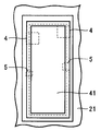
図15に、テストパネルの第1領域における1個の画素の拡大概略平面図を示す。図16に、テストパネルの第2領域における1個の画素の拡大概略平面図を示す。図15および図16は、有機EL層を形成する前の段階におけるそれぞれの画素の概略平面図である。すなわち、画素電極の表面に、画素分離隔壁を形成したときの拡大概略平面図である。 FIG. 15 shows an enlarged schematic plan view of one pixel in the first region of the test panel. FIG. 16 shows an enlarged schematic plan view of one pixel in the second region of the test panel. FIG. 15 and FIG. 16 are schematic plan views of respective pixels in a stage before forming the organic EL layer. That is, it is an enlarged schematic plan view when a pixel separation partition is formed on the surface of the pixel electrode.
図15に示すように、テストパネルの第1領域においては、画素電極41の露出している部分の周りにおいては、画素分離隔壁21の外縁部が配置されている。この領域に、TFT4や、コンタクト5が形成されている領域においても、凹凸などの形状は観察されなかった。
As shown in FIG. 15, in the first region of the test panel, the outer edge portion of the pixel
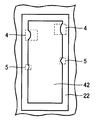
これに対して、図16に示すように、テストパネルの第2領域においては、層間絶縁膜に窪み部が形成されていないため、画素電極42の露出している部分の周りに、凹凸またはこれに類するうねりが観察された。凹凸またはうねりは、TFT4やコンタクト5が形成されている領域に発現した。このように、画素電極に凹凸が発現している部分においては、画素分離隔壁22の外縁部の厚さが他の部分と異なっていた。すなわち、外縁部にも凹凸が生じていた。
On the other hand, as shown in FIG. 16, in the second region of the test panel, no depression is formed in the interlayer insulating film. A similar swell was observed. Irregularities or waviness appeared in the region where the
顕微鏡による観察により、本実施の形態における第1の有機EL表示装置においては、画素分離隔壁の外縁部で凹凸などを観察することはできず、画素分離隔壁の形状が安定して形成されていた。 By observation with a microscope, in the first organic EL display device according to the present embodiment, it was impossible to observe irregularities at the outer edge of the pixel separation partition, and the shape of the pixel separation partition was stably formed. .
次に、画素電極の表面に、有機EL層を形成する。有機EL層は、画素領域全体を覆うように形成する。有機EL層は、端部が画素分離隔壁の外縁部に乗り上げるように形成する。次に、有機EL層の表面および画素分離隔壁の表面に対向電極を形成して、有機EL表示装置を製造する。この製造方法により、第1領域および第2領域を有する同一のテストパネルを10個製造した。テストパネルにおいては、それぞれの領域に1000個の画素を形成した。 Next, an organic EL layer is formed on the surface of the pixel electrode. The organic EL layer is formed so as to cover the entire pixel region. The organic EL layer is formed so that the end portion runs over the outer edge portion of the pixel separation partition wall. Next, a counter electrode is formed on the surface of the organic EL layer and the surface of the pixel separation partition wall to manufacture an organic EL display device. Ten identical test panels having the first region and the second region were manufactured by this manufacturing method. In the test panel, 1000 pixels were formed in each region.
次に、発光試験を行なった。発光試験においては、それぞれの領域毎に表示欠陥の数を数えた。また、表示欠陥の詳細な原因を確認した。 Next, a light emission test was performed. In the light emission test, the number of display defects was counted for each region. Moreover, the detailed cause of the display defect was confirmed.
層間絶縁膜に窪み部を形成したテストパネルの第1領域においては、0.5%以上2%以下の表示欠陥の画素が確認された。この画素を顕微鏡で詳細に観察したところ、そのすべてにおいて、画素電極の表面に残存する異物によって、画素電極と対向電極とが電気的に短絡していることが分かった。画素分離隔壁の外縁部における有機EL層の被膜性に起因する欠陥は観察されなかった。 In the first region of the test panel in which the depressions were formed in the interlayer insulating film, pixels having display defects of 0.5% or more and 2% or less were confirmed. When these pixels were observed in detail with a microscope, it was found that in all of them, the pixel electrode and the counter electrode were electrically short-circuited by foreign matters remaining on the surface of the pixel electrode. Defects due to the coating properties of the organic EL layer at the outer edge of the pixel separation partition were not observed.
テストパネルの第2領域においては、約10%以上15%以下の表示欠陥の画素が確認された。この表示欠陥の画素のうち、200画素について顕微鏡で詳細に観察したところ、23箇所においては、画素電極の表面に残存する異物が確認された。その他の箇所については、画素電極の表面に残存する異物を確認することはできなかった。 In the second region of the test panel, display defect pixels of about 10% to 15% were confirmed. Of these display defective pixels, 200 pixels were observed in detail with a microscope. As a result, in 23 locations, foreign matter remaining on the surface of the pixel electrode was confirmed. In other places, foreign matters remaining on the surface of the pixel electrode could not be confirmed.
さらに、10個のテストパネル中から2個の異物が確認されなかった表示欠陥を有するテストパネルについて抜き取った。それぞれの表示欠陥の画素について、画素分離隔壁の外縁部を中心に、電子顕微鏡でより詳細に断面の観察を行なった。この結果、画素分離隔壁の外縁部の外面が基板の表面に対して傾斜する角度が約70°と大きくなっている箇所があり、加えてこの部分においては、有機EL層の被膜性が悪いために、画素電極と対向電極とが短絡していることが分かった。 Further, a test panel having a display defect in which two foreign substances were not confirmed from the ten test panels was extracted. For each display defect pixel, the cross section was observed in more detail with an electron microscope, centering on the outer edge of the pixel separation partition wall. As a result, there is a portion where the angle at which the outer surface of the outer edge of the pixel separation partition wall is inclined with respect to the surface of the substrate is as large as about 70 °. Further, it was found that the pixel electrode and the counter electrode are short-circuited.
このように、本実施の形態の有機EL表示装置においては、有機EL層の被膜性が向上して、画素電極と対向電極との短絡を抑制することができた。 Thus, in the organic EL display device of the present embodiment, the film property of the organic EL layer was improved, and a short circuit between the pixel electrode and the counter electrode could be suppressed.
次に、製造した10個のテストパネルのうち8個について、1000時間の連続点灯試験を行なった。この結果、テストパネルの第2領域においては、表示欠陥の画素が約20%以上25%以下まで増加した。すなわち、連続点灯を行なうことにより、表示欠陥が約10%増加した。これに対して、第1領域においては、連続点灯を行なっても、顕微鏡で観察される異物による原因以外の表示欠陥を確認することはできなかった。この連続点灯試験の結果により、有機EL表示装置の信頼性が向上することについても確認することができた。 Next, a continuous lighting test for 1000 hours was performed on 8 of 10 manufactured test panels. As a result, in the second region of the test panel, the number of display defect pixels increased from about 20% to 25%. In other words, display defects increased by about 10% by performing continuous lighting. On the other hand, in the first region, even if continuous lighting was performed, display defects other than the cause due to the foreign matter observed with a microscope could not be confirmed. From the result of this continuous lighting test, it was confirmed that the reliability of the organic EL display device was improved.
本実施の形態においては、アクティブマトリックス駆動を行なう能動素子として、基板の表面にTFTが形成された例に採り上げて説明したが、この形態に限られず、アクティブマトリックス駆動を行なう能動素子については、任意の素子を用いることができる。 In the present embodiment, the active element for performing active matrix driving has been described as an example of an active element that performs TFT driving on the surface of the substrate. However, the present invention is not limited to this form, and any active element for performing active matrix driving may be used. These elements can be used.
本実施の形態においては、トップエミッション構造を有する有機EL表示装置を例に採り上げて説明したが、この形態に限られず、有機EL層にて発光した光を基板の下面より取出すいわゆるボトムエミッション構造を有する有機EL表示装置にも本発明を適用することができる。 In this embodiment, an organic EL display device having a top emission structure has been described as an example. However, the present invention is not limited to this form, and a so-called bottom emission structure in which light emitted from the organic EL layer is extracted from the lower surface of the substrate. The present invention can also be applied to an organic EL display device having the same.
(実施の形態2)
図17から図19を参照して、本発明に基づく実施の形態2における有機EL表示装置および有機EL表示装置の製造方法について説明する。
(Embodiment 2)
With reference to FIGS. 17 to 19, an organic EL display device and a method for manufacturing the organic EL display device according to the second embodiment of the present invention will be described.
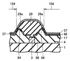
図17は、本実施の形態における第1の有機EL表示装置の概略断面図である。図17は、それぞれの画素同士に挟まれる領域の部分における概略断面図である。有機EL表示装置が、基板1を備え、基板1の表面にTFT4や配線3などの電気回路が形成されていることは、実施の形態1と同様である。本実施の形態においては、窪み部の代わりに隆起部が層間絶縁膜に形成されている。
FIG. 17 is a schematic cross-sectional view of the first organic EL display device in the present embodiment. FIG. 17 is a schematic cross-sectional view of a region sandwiched between the pixels. The organic EL display device includes the
本実施の形態における有機EL表示装置は、基板1の上側に形成された絶縁膜として層間絶縁膜14を有する。層間絶縁膜14は、少なくとも一部が矢印154に示す画素の領域同士の間に配置されるように形成された隆起部83を有する。
The organic EL display device in the present embodiment has an
本実施の形態における隆起部83は、それぞれの画素同士の間の領域を含むように形成されている。隆起部83は、外側に突出するように形成されている。隆起部83は、断面形状がほぼ台形に形成されている。隆起部83は、中央部に向かうにつれて、徐々に層間絶縁膜11の厚さが厚くなるように形成されている。隆起部83は、画素を取り囲むように形成されている。隆起部83は、画素に沿って形成されている。
The raised
隆起部83は、外面を有する。外面は、側面83aおよび頂面83bを有する。側面83aは、基板1の表面に対して傾斜するように形成されている。隆起部83は、側面83aの部分の厚さが頂面83bに向かって徐々に厚くなるように形成されている。隆起部83は、コンタクトホール83cを有する。
The raised
有機EL表示装置は、層間絶縁膜14の上側に形成され、それぞれの画素毎に電気的に分離されて形成された画素電極44を有する。
The organic EL display device has a
本実施の形態における有機EL表示装置は、層間絶縁膜14の上側に形成され、それぞれの画素同士の間に配置された画素分離隔壁24を有する。本実施の形態における画素分離隔壁24は、断面形状がほぼ台形になるように形成されている。画素分離隔壁24は、隆起部83のほぼ中央に形成されている。画素分離隔壁24は、隆起部83が形成されている範囲内に形成されている。
The organic EL display device in the present embodiment has a pixel
画素分離隔壁24は、外縁部を含む。画素分離隔壁24の外縁部は、隆起部83の外面の領域に配置されている。外縁部は、縁24aを有する。画素分離隔壁24は、外縁部が縁24aに向かって厚さが徐々に薄くなるように形成されている。縁24aは、層間絶縁膜14の隆起部83の外面のうち側面83aの領域に配置されている。
The
有機EL表示装置は、画素電極44の表面に形成された有機EL層34を有する。有機EL層34は、層間絶縁膜14の平面的な部分から、隆起部83の側面83aの領域まで形成されている。有機EL層34は、端部が隆起部83に乗り上げている。有機EL層34および画素分離隔壁24の表面には、対向電極54が形成されている。
The organic EL display device has an
図18に、本実施の形態における画素分離隔壁の外縁部の部分の拡大概略断面図を示す。有機EL層34は、曲がり部34aを有する。本実施の形態における隆起部83は、基板1の主表面に対する側面83aの傾斜角度θ4が、30°になるように形成されている。基板1の表面に対する傾斜角度θ4は、3°以上80°以下が好ましい。
FIG. 18 is an enlarged schematic cross-sectional view of the outer edge portion of the pixel separation partition wall in the present embodiment. The
また、本実施の形態における隆起部83は、基板1の表面に対する画素分離隔壁24の外縁部の外面の傾斜角度θ5は、50°になるように形成されている。基板1の表面に対する画素分離隔壁24の外縁部の傾斜角度θ5は、3°以上50°以下の範囲内で形成することが好ましい。本実施の形態においては、層間絶縁膜14の隆起部83の側面83aが傾斜して、画素分離隔壁24の外縁部の外面が傾斜している。これらのそれぞれの傾斜面が互いになす角度θ6は、20°になるように形成されている。
Further, the raised
図17を参照して、隆起部83の幅W1は、画素分離隔壁24の幅W2よりも大きくなるように形成されている。実施の形態1と同様に、隆起部83の幅W1は、製造精度の観点から、画素分離隔壁24の幅W2よりも、0.2μm以上大きくなるように形成されることが好ましい。
With reference to FIG. 17, the width W <b> 1 of the raised
本実施の形態における有機EL表示装置においては、層間絶縁膜14に隆起部83が形成され、隆起部83の外面の領域に、画素分離隔壁24の外縁部が配置されている。この構成により、実施の形態1と同様に、画素分離隔壁24の外縁部における有機EL層34の被膜性を向上することができる。この結果、画素電極44と対向電極54との短絡を抑制することができる。
In the organic EL display device according to the present embodiment, the raised
層間絶縁膜の表面の凹凸およびそれに類するうねりに比べて、桁違いに大きな隆起部を形成することによって、層間絶縁膜の表面の凹凸およびこれに類するうねりを実質的に吸収することができ、画素分離隔壁の外縁部における形状への影響を小さくすることができる。たとえば、層間絶縁膜の表面の凹凸およびそれに類するうねりの最大高低差の10倍以上の高さを有する隆起部を形成することにより表面の凹凸を小さくできる。 Compared to the unevenness on the surface of the interlayer insulating film and the undulations similar to that, it is possible to substantially absorb the unevenness on the surface of the interlayer insulating film and the similar undulations by forming an extremely large ridge. The influence on the shape at the outer edge of the separation partition wall can be reduced. For example, the surface unevenness can be reduced by forming a raised portion having a height of 10 times or more of the maximum height difference between the surface unevenness of the interlayer insulating film and the undulation similar thereto.
または、隆起部を形成しないときの層間絶縁膜の表面の凹凸およびこれに類するうねりの最大高低差は、層間絶縁膜の厚さの0.1%以上5%以下である。層間絶縁膜の隆起部においては、隆起部83の頂面83bの部分における厚さが、隆起部83が形成されていない領域の厚さの120%以上190%以下が好ましい。
Alternatively, the unevenness on the surface of the interlayer insulating film and the undulation similar to this when the raised portion is not formed are 0.1% or more and 5% or less of the thickness of the interlayer insulating film. In the raised portion of the interlayer insulating film, the thickness of the
本実施の形態においては、隆起部が頂面および側面を有するが、この形態に限られず、隆起部は、頂面を有しなくても構わない。たとえば、隆起部の断面形状が、円弧状に形成されていても構わない。 In the present embodiment, the raised portion has a top surface and a side surface, but the present invention is not limited to this configuration, and the raised portion may not have the top surface. For example, the cross-sectional shape of the raised portion may be formed in an arc shape.
また、本実施の形態における第1の有機EL表示装置においては、画素分離隔壁24の縁24aが、隆起部83の側面83aの領域に配置されているが、この形態に限られず、画素分離隔壁は、縁が隆起部の形成されている領域に配置されていれば構わない。
Further, in the first organic EL display device according to the present embodiment, the
図19に、本実施の形態における第2の有機EL表示装置の概略断面図を示す。第2の有機EL表示装置は、画素分離隔壁25を有する。画素分離隔壁25の縁25aは、隆起部83の頂面83bと側面83aとの境界部分に配置されている。この構成を採用することによっても、有機EL層34の被膜性が向上して、画素電極44と対向電極54との短絡を抑制することができる。
FIG. 19 is a schematic cross-sectional view of the second organic EL display device in the present embodiment. The second organic EL display device has a
本実施の形態における有機EL表示装置の製造方法においては、基板の上側に絶縁膜としての層間絶縁膜を形成する絶縁膜形成工程と、層間絶縁膜の上側の画素同士の間に分離隔壁を形成する分離隔壁形成工程とを含む。絶縁膜形成工程は、画素同士の間の少なくとも一部を含むように、画素に沿って隆起部を形成する工程を含む。分離隔壁形成工程は、隆起部の外面の領域に外縁部が配置されるように、画素分離隔壁を形成する工程を含む。この製造方法により、実施の形態1と同様に、画素欠陥を抑制した有機EL表示装置の製造方法を提供することができる。 In the manufacturing method of the organic EL display device according to the present embodiment, an isolation partition is formed between the insulating film forming step of forming an interlayer insulating film as an insulating film on the upper side of the substrate and the pixels on the upper side of the interlayer insulating film. Separating partition forming step. The insulating film forming step includes a step of forming a raised portion along the pixel so as to include at least a part between the pixels. The separation partition forming step includes a step of forming the pixel separation partition so that the outer edge portion is disposed in the region of the outer surface of the raised portion. By this manufacturing method, a method for manufacturing an organic EL display device in which pixel defects are suppressed can be provided as in the first embodiment.
本実施の形態においては、絶縁膜形成工程において、実施の形態1の窪み部の代わりに隆起部を形成する。隆起部は、実施の形態1と同様に、たとえば、フォトリソグラフィ法において、ハーフトーンマスクを用いることにより形成することができる。また、分離隔壁形成工程において、隆起部の外面に外縁部が配置されるように画素分離隔壁を形成する。 In the present embodiment, in the insulating film forming step, a raised portion is formed instead of the recessed portion in the first embodiment. Similar to the first embodiment, the raised portion can be formed by using a halftone mask in, for example, a photolithography method. Further, in the separation partition forming step, the pixel separation partition is formed so that the outer edge portion is disposed on the outer surface of the raised portion.
次に、実施の形態1と同様にテストパネルを製造して試験を行なった。図13を参照して、テストパネル71の第1領域71aに、本実施の形態における第1の有機EL表示装置を形成した。第2領域71bに、実施の形態1と同じ比較例の有機EL表示装置(図14参照)を形成した。
Next, a test panel was manufactured and tested in the same manner as in the first embodiment. Referring to FIG. 13, the first organic EL display device according to the present embodiment was formed in
基板の表面に、TFTなどの電気回路を形成した。次に、基板の表面に絶縁膜としての層間絶縁膜を形成する絶縁膜形成工程を行なう。本実施の形態においては、公知の感光性を有するアクリル樹脂を用いて、厚さが2μmになるように一様のアクリル樹脂膜を形成した。 An electric circuit such as a TFT was formed on the surface of the substrate. Next, an insulating film forming step for forming an interlayer insulating film as an insulating film on the surface of the substrate is performed. In the present embodiment, a uniform acrylic resin film is formed so as to have a thickness of 2 μm using a known photosensitive acrylic resin.
次に、フォトリソグラフィ法によって、層間絶縁膜にコンタクトホールなどのパターンを形成する。このときに、テストパネル71の第1領域71aにおいては、層間絶縁膜の隆起部を形成する。本実施の形態においては、画素同士の間の領域を含むように隆起部を形成する。隆起部は、平面的な部分から連続して隆起する部分を形成する。
Next, a pattern such as a contact hole is formed in the interlayer insulating film by photolithography. At this time, a raised portion of the interlayer insulating film is formed in the
隆起部の形成においては、実施の形態1と同様に、ハーフトーンマスクを用いて露光量を最適化する、または、露光条件を制御して露光量を調整することによって形成することができる。本実施の形態においては、図18を参照して傾斜角度θ4が、30°になるように層間絶縁膜14を形成した。
In the formation of the raised portion, similarly to the first embodiment, the exposure amount can be optimized by using a halftone mask, or the exposure amount can be adjusted by controlling the exposure conditions. In the present embodiment, referring to FIG. 18,
次に、アクリル処理溶液で、コンタクトホールの内部に残存する残渣物を除去した。次に、画素電極を形成する画素電極形成工程を行なった。画素電極の形成においては、スパッタ法によって、厚さが200nmのCr膜を形成した。フォトリソグラフィ法によりCr膜のパターニングを行なって不連続部等を形成した。この工程においては、隆起部の形状に沿って一様な厚さのCr膜を形成することができた。 Next, the residue remaining inside the contact hole was removed with an acrylic treatment solution. Next, a pixel electrode forming step for forming a pixel electrode was performed. In forming the pixel electrode, a Cr film having a thickness of 200 nm was formed by sputtering. The Cr film was patterned by photolithography to form discontinuities and the like. In this step, a Cr film having a uniform thickness could be formed along the shape of the raised portion.
次に、画素分離隔壁を形成する分離隔壁形成工程を行なう。本実施の形態においては、感光性を有するポリイミド膜を一様な厚さで形成した後に、フォトリソグラフィ法によりパターニングを行なう。画素分離隔壁は、層間絶縁膜に形成した隆起部と同様に、フォトマスクおよび処理条件等を調整することにより、画素分離隔壁の外縁部が徐々に薄くなるように形成する。 Next, a separation partition forming step for forming a pixel separation partition is performed. In this embodiment mode, after forming a photosensitive polyimide film with a uniform thickness, patterning is performed by a photolithography method. Similar to the raised portion formed in the interlayer insulating film, the pixel separating partition is formed such that the outer edge of the pixel separating partition is gradually thinned by adjusting the photomask and processing conditions.
本実施の形態における分離隔壁形成工程においては、画素電極の表面に、厚さがほぼ2μmになるようにポリイミド膜を塗工した。ここで、テストパネル71の第1領域71aにおいては、厚さが2μmになるように画素分離隔壁となるポリイミドを塗工しているが、層間絶縁膜の隆起部の断面形状に沿って、ポリイミドが画素分離隔壁の中央部に近づくにつれて徐々に薄く形成される。本実施の形態においては、隆起部の頂面となるべき部分のポリイミド膜の厚さは1μmであった。
In the separation partition wall forming step in the present embodiment, a polyimide film was applied on the surface of the pixel electrode so that the thickness was approximately 2 μm. Here, in the
次に、ポリイミド膜を、130℃でプリベークした。次に、フォトマスクを用いて露光を行なった。次に、現像処理によって露光されたパターンが除去されて、所望の形状の画素分離隔壁を得た。画素分離隔壁は、隆起部のほぼ中央部分に形成した。 Next, the polyimide film was pre-baked at 130 ° C. Next, exposure was performed using a photomask. Next, the exposed pattern was removed by development processing to obtain a pixel separation partition wall having a desired shape. The pixel separation partition was formed at the substantially central portion of the raised portion.
図18を参照して、テストパネル71の第1領域71aにおいては、画素分離隔壁の外縁部における傾斜角度θ5が、50°になるように形成した。また、図17を参照して、隆起部83の幅W1が、画素分離隔壁の幅W2よりも2μm大きくなるように形成した。すなわち、片側が1μmの差を有するように形成した。また、第1領域71aの隆起部83の頂面83bの部分の厚さが、隆起部83の周りの部分の厚さの150%になるように隆起部を形成した。
Referring to FIG. 18, the
このように画素分離隔壁まで製造したテストパネル71において、実施の形態1と同様に、顕微鏡により観察を行なったところ、第2領域71bにおいては、TFTやコンタクトなどの電気回路の凹凸に対応して、画素分離隔壁の外縁部において、凹凸やそれに類するうねりが観察された。一方で、テストパネル71の第1領域71aについて顕微鏡観察を行なったところ、第2領域71bで観察された凹凸などは観察されなかった。画素分離隔壁は、形状が安定して形成されていた。
In the
本実施の形態においては、実施の形態1と同様に、層間絶縁膜の表面の段差が、配線やコンタクトホールに起因する層間絶縁膜表面の凹凸に比べて大きいため、層間絶縁膜の表面の凹凸やうねりの影響が小さくなったと考えられる。 In this embodiment, since the step on the surface of the interlayer insulating film is larger than the unevenness on the surface of the interlayer insulating film caused by wiring and contact holes, the surface unevenness on the surface of the interlayer insulating film is the same as in the first embodiment. It is thought that the influence of swell was reduced.
次に、本実施の形態におけるテストパネルの第1領域および第2領域に、有機EL層および対向電極などを公知の方法により形成して、有機EL表示装置を製造した。この製造方法により、同じテストパネルを10個製造した。テストパネルにおいては、それぞれの領域に1000個の画素を形成した。 Next, an organic EL display device was manufactured by forming an organic EL layer, a counter electrode, and the like in the first region and the second region of the test panel according to the present embodiment by a known method. Ten same test panels were manufactured by this manufacturing method. In the test panel, 1000 pixels were formed in each region.
次に、発光試験を行なった。発光試験においては、それぞれの領域毎に表示欠陥の数を数えた。また、表示欠陥の詳細な原因を確認した。 Next, a light emission test was performed. In the light emission test, the number of display defects was counted for each region. Moreover, the detailed cause of the display defect was confirmed.
層間絶縁膜に隆起部を形成したテストパネルの第1領域においては、1%以上3%以下の表示欠陥の画素が確認された。この画素を顕微鏡で詳細に観察したところ、そのすべてにおいて、画素電極の表面に残存する異物によって、画素電極と対向電極とが電気的に短絡していることが分かった。画素分離隔壁の外縁部における有機EL層の被膜性に起因する欠陥は観察されなかった。 In the first region of the test panel in which the raised portion is formed in the interlayer insulating film, pixels having display defects of 1% or more and 3% or less were confirmed. When this pixel was observed in detail with a microscope, it was found that in all of the pixels, the pixel electrode and the counter electrode were electrically short-circuited by foreign matters remaining on the surface of the pixel electrode. Defects due to the coating properties of the organic EL layer at the outer edge of the pixel separation partition were not observed.
一方で、第2領域においては、1000画素中の約8%以上14%以下で表示欠陥の画素が確認された。この表示欠陥の画素のうち、300画素を顕微鏡で詳細に観察したところ、32箇所においては、画素電極の表面に残存する異物が確認されたが、その他の箇所については異物は確認されなかった。 On the other hand, in the second region, display defective pixels were confirmed in about 8% to 14% of the 1000 pixels. Of these display defect pixels, 300 pixels were observed in detail with a microscope. As a result, foreign matter remaining on the surface of the pixel electrode was confirmed in 32 locations, but no foreign matter was confirmed in other locations.
さらに、異物が確認されなかった表示欠陥画素について、画素分離隔壁の外縁部を中心に、顕微鏡でより詳細な断面の観察を行なったところ、実施の形態1と同様に、基板の表面に対して画素分離隔壁の外縁部の外面の傾斜角度が約70°と高くなっている箇所があった。さらに、この部分においては、有機EL層の被膜性が悪いために、画素電極と対向電極とが接触している箇所があった。 Further, for the display defective pixel in which no foreign matter was confirmed, a more detailed cross-section was observed with a microscope centering on the outer edge of the pixel separation partition wall. There was a portion where the inclination angle of the outer surface of the outer edge of the pixel separation partition wall was as high as about 70 °. Further, in this portion, the pixel electrode and the counter electrode are in contact with each other because the coating property of the organic EL layer is poor.
このように、本実施の形態における有機EL表示装置においては、有機EL層の被膜性が向上して、画素電極と対向電極との短絡を抑制することができた。 Thus, in the organic EL display device according to the present embodiment, the film property of the organic EL layer was improved, and a short circuit between the pixel electrode and the counter electrode could be suppressed.
次に、製造した10個のテストパネルのうち8個について、1000時間の連続点灯試験を行なったところ、第2領域での表示欠陥の画素は、約20%まで増加した。これに対して、第1領域においては、連続点灯を行なっても顕微鏡で観察される異物による原因以外の表示欠陥を確認することはできなかった。 Next, a continuous lighting test for 1000 hours was performed on 8 of 10 manufactured test panels. As a result, the number of display defect pixels in the second region increased to about 20%. On the other hand, in the first region, it was not possible to confirm display defects other than the cause due to the foreign matter observed with a microscope even if continuous lighting was performed.
この連続点灯試験の結果により、本実施の形態における有機EL表示装置の信頼性が向上することについても確認することができた。 From the result of this continuous lighting test, it was confirmed that the reliability of the organic EL display device in this embodiment is improved.
上記以外の構成、作用、効果および製造方法については、実施の形態1と同様であるのでここでは説明を繰返さない。 Since the configuration, operation, effect, and manufacturing method other than those described above are the same as those in the first embodiment, description thereof will not be repeated here.
(実施の形態3)
図20から図27を参照して、本発明に基づく実施の形態3における有機EL表示装置について説明する。本実施の形態においては、層間絶縁膜に、様々な隆起部または窪み部を形成した有機EL表示装置について説明する。本実施の形態においては、互いに隣り合う画素同士の間に、隆起部および突起部のうち少なくとも一方が、複数形成されている。
(Embodiment 3)
With reference to FIGS. 20 to 27, an organic EL display device according to a third embodiment of the present invention will be described. In the present embodiment, an organic EL display device in which various raised portions or recessed portions are formed in an interlayer insulating film will be described. In the present embodiment, a plurality of at least one of the raised portion and the protruding portion is formed between adjacent pixels.
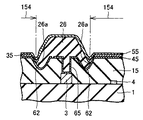
図20は、本実施の形態における第1の有機EL表示装置の概略断面図である。第1の有機EL表示装置は、層間絶縁膜15を有する。層間絶縁膜15は、コンタクトホール65を有する。層間絶縁膜15は、窪み部62を有する。窪み部62は、コンタクトホール65を挟むように形成されている。窪み部62は、断面においてコンタクトホール65の両側に形成されている。窪み部62は、それぞれの画素に沿うように延びている。窪み部62は、画素の側の傾斜面(画素の中心に向かう傾斜面)および窪み部62同士が対向する側の傾斜面を有する。層間絶縁膜15の表面には、画素電極45が形成されている。
FIG. 20 is a schematic cross-sectional view of the first organic EL display device in the present embodiment. The first organic EL display device has an
第1の有機EL表示装置は、画素分離隔壁26を有する。画素分離隔壁26は、複数の窪み部62で挟まれる領域に形成されている。画素分離隔壁26は、縁26aを有する。縁26aは、窪み部62の内面に配置されている。画素分離隔壁26の縁26aは、窪み部62の画素の側の傾斜面に配置されている。
The first organic EL display device has a
画素電極45の表面には、有機EL層35が配置されている。有機EL層35は、端部が、画素分離隔壁26の縁26aの部分の表面に乗り上げるように形成されている。有機EL層35および画素分離隔壁26の表面には、対向電極55が形成されている。
An
図21に、本実施の形態における第2の有機EL表示装置の概略断面図を示す。第2の有機EL表示装置は、画素分離隔壁の縁の位置が、第1の有機EL表示装置と異なる。第2の有機EL表示装置は、層間絶縁膜16を有する。層間絶縁膜16は、窪み部62を有する。
FIG. 21 is a schematic cross-sectional view of the second organic EL display device in the present embodiment. The second organic EL display device is different from the first organic EL display device in the position of the edge of the pixel separation partition. The second organic EL display device has an
第2の有機EL表示装置は、画素分離隔壁27を有する。画素分離隔壁27は、縁27aを有する。縁27aは、窪み部62同士が対向する側の傾斜面および画素の側の傾斜面のうち、窪み部62同士が対向する側の傾斜面に配置されている。
The second organic EL display device has a
第2の有機EL表示装置は、有機EL層36を有する。有機EL層36は、窪み部62の一部の領域に配置されている。有機EL層36は、端部が画素分離隔壁27に乗り上げるように形成されている。第2の有機EL表示装置は、有機EL層36の表面に形成された対向電極56を有する。
The second organic EL display device has an
本発明においては、本実施の形態における第1の有機EL表示装置および第2の有機EL表示装置のように、それぞれの画素同士の間に、複数の窪み部が形成されていても構わない。また、第1の有機EL表示装置および第2の有機EL表示装置においては、窪み部の傾斜面に、画素分離隔壁の縁が配置されるように画素分離隔壁が形成されているが、この形態に限られず、それぞれの窪み部の底点または底面に、画素分離隔壁の外縁部が配置されていても構わない。 In the present invention, as in the first organic EL display device and the second organic EL display device in the present embodiment, a plurality of depressions may be formed between the respective pixels. Further, in the first organic EL display device and the second organic EL display device, the pixel separation partition is formed so that the edge of the pixel separation partition is disposed on the inclined surface of the recess. However, the outer edge portion of the pixel separation partition may be arranged at the bottom or bottom surface of each recess.
図22に、本実施の形態における第3の有機EL表示装置の概略断面図を示す。第3の有機EL表示装置は、層間絶縁膜16を有する。層間絶縁膜16は、隆起部84を有する。層間絶縁膜16は、コンタクトホール66を有する。コンタクトホール66は、それぞれの画素同士の間に配置されている。隆起部84は、画素同士の間に2個形成されている。隆起部84は、コンタクトホール66と画素との間の領域に配置されている。層間絶縁膜16の表面には、画素電極46が形成されている。
FIG. 22 is a schematic cross-sectional view of the third organic EL display device in the present embodiment. The third organic EL display device has an
第3の有機EL表示装置は、画素分離隔壁28を有する。画素分離隔壁28は、断面において、2個の隆起部84で挟まれる領域に形成されている。画素分離隔壁28は、縁28aを有する。隆起部84は、画素の側の傾斜面および隆起部84同士が対向する側の傾斜面を有する。画素分離隔壁28の縁28aは、傾斜面のうち、隆起部84同士が対向する側の傾斜面に配置されている。
The third organic EL display device has a
画素電極46の表面には、有機EL層36が配置されている。有機EL層36は、隆起部84の傾斜面のうち、画素の側の傾斜面および隆起部同士が対向する側の傾斜面の一部に配置されている。有機EL層36の端部は、画素分離隔壁28の外縁部に乗り上げるように形成されている。有機EL層36および画素分離隔壁28の表面には、対向電極56が配置されている。
An
図23に、本実施の形態における第4の有機EL表示装置の概略断面図を示す。第4の有機EL表示装置は、本実施の形態における第3の有機EL表示装置と、画素分離隔壁の部分が異なる。 FIG. 23 is a schematic cross-sectional view of the fourth organic EL display device in the present embodiment. The fourth organic EL display device is different from the third organic EL display device in the present embodiment in the pixel separation partition.
第4の有機EL表示装置は、層間絶縁膜17を有する。層間絶縁膜17は、隆起部84を有する。第4の有機EL表示装置は、画素分離隔壁29を有する。画素分離隔壁29は、外縁部に縁29aを有する。縁29aは、隆起部84の画素の側の傾斜面および隆起部84同士が対向する側の傾斜面のうち、画素の側の傾斜面に配置されている。
The fourth organic EL display device has an interlayer insulating film 17. The interlayer insulating film 17 has a raised
第4の有機EL表示装置は、有機EL層37を有する。有機EL層37は、端部が、画素分離隔壁29の外縁部に乗り上げるように形成されている。有機EL層37および画素分離隔壁29の表面には対向電極57が形成されている。
The fourth organic EL display device has an organic EL layer 37. The organic EL layer 37 is formed so that the end portion runs over the outer edge portion of the pixel
本発明においては、第3の有機EL表示装置および第4の有機EL表示装置のように、それぞれの画素同士の間に、複数の隆起部が形成されていても構わない。また、第3の有機EL表示装置および第4の有機EL表示装置においては、隆起部の傾斜面に画素分離隔壁の縁が配置されるように画素分離隔壁が形成されているが、この形態に限られず、それぞれの隆起部の頂点または頂面に、画素分離隔壁の外縁部が配置されていても構わない。 In the present invention, like the third organic EL display device and the fourth organic EL display device, a plurality of raised portions may be formed between the respective pixels. Further, in the third organic EL display device and the fourth organic EL display device, the pixel separation partition is formed so that the edge of the pixel separation partition is disposed on the inclined surface of the raised portion. The outer edge portion of the pixel separation partition may be arranged at the apex or top surface of each raised portion.
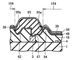
図24に、本実施の形態における第5の有機EL表示装置の概略断面図を示す。第5の有機EL表示装置は、層間絶縁膜18を有する。層間絶縁膜18は隆起部84を有する。層間絶縁膜18は、窪み部62を有する。本実施の形態においては、互いに隣り合う画素同士の間に、隆起部84および窪み部62が形成されている。隆起部84および窪み部62は、画素の側の傾斜面および窪み部と隆起部が対向する側の傾斜面を有する。層間絶縁膜18は、コンタクトホール67を有する。層間絶縁膜18の表面には、画素電極48が形成されている。
FIG. 24 is a schematic cross-sectional view of the fifth organic EL display device in the present embodiment. The fifth organic EL display device has an
第5の有機EL表示装置は、画素分離隔壁95を有する。画素分離隔壁95は、縁95a,95bを有する。縁95aは、隆起部84の傾斜面のうち、窪み部と隆起部が対向する側の傾斜面に配置されている。縁95bは、窪み部62の傾斜面のうち、画素の側の傾斜面に配置されている。
The fifth organic EL display device has a
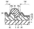
第5の有機EL表示装置は、有機EL層38を有する。有機EL層38は、画素分離隔壁95の縁95a,95bを含む外縁部に、端部が乗り上げるように形成されている。有機EL層38および画素分離隔壁95の表面には、対向電極58が形成されている。
The fifth organic EL display device has an
図25に、本実施の形態における第6の有機EL表示装置の概略断面図を示す。第6の有機EL表示装置は、画素分離隔壁の形状が第5の有機EL表示装置と異なる。 FIG. 25 is a schematic sectional view of a sixth organic EL display device in the present embodiment. The sixth organic EL display device is different from the fifth organic EL display device in the shape of the pixel separation partition.
第6の有機EL表示装置は、画素分離隔壁96を有する。画素分離隔壁96は、縁96a,96bを有する。縁96aは、隆起部84の傾斜面のうち、窪み部と隆起部とが対向する側の傾斜面に配置されている。縁96bは、窪み部62の傾斜面のうち、窪み部と隆起部とが対向する側の傾斜面に配置されている。画素電極48の表面には、有機EL層39が形成されている。有機EL層39および画素分離隔壁96の表面には、対向電極59が形成されている。
The sixth organic EL display device has a
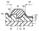
図26に、本実施の形態における第7の有機EL表示装置の概略断面図を示す。第7の有機EL表示装置は、画素分離隔壁の形状が第5の有機EL表示装置と異なる。 FIG. 26 shows a schematic cross-sectional view of a seventh organic EL display device in the present embodiment. The seventh organic EL display device is different from the fifth organic EL display device in the shape of the pixel separation partition.
第7の有機EL表示装置は、画素分離隔壁97を有する。画素分離隔壁97は、縁97a,97bを有する。縁97aは、隆起部84の傾斜面のうち、画素の側の傾斜面に配置されている。縁97bは、窪み部62の傾斜面のうち、画素の側の傾斜面に配置されている。画素電極48の表面には、有機EL層121が形成されている。有機EL層121および画素分離隔壁97の表面には、対向電極106が形成されている。
The seventh organic EL display device has a
図27に、本実施の形態における第8の有機EL表示装置の概略断面図を示す。第8の有機EL表示装置は、画素分離隔壁の形状が第5の有機EL表示装置と異なる。 FIG. 27 shows a schematic cross-sectional view of the eighth organic EL display device in the present embodiment. The eighth organic EL display device is different from the fifth organic EL display device in the shape of the pixel separation partition.
第8の有機EL表示装置は、画素分離隔壁98を有する。画素分離隔壁98は、縁98a,98bを有する。縁98aは、隆起部84の傾斜面のうち、画素の側の傾斜面に配置されている。縁98bは、窪み部62の傾斜面のうち、窪み部と隆起部とが対向する側の傾斜面に配置されている。画素電極48の表面には、有機EL層122が形成されている。有機EL層122および画素分離隔壁98の表面には、対向電極107が形成されている。
The eighth organic EL display device has a
本発明においては、第5から第8の有機EL表示装置のように、それぞれの画素同士の間に、窪み部および隆起部が形成されていても構わない。 In the present invention, as in the fifth to eighth organic EL display devices, recesses and ridges may be formed between the respective pixels.
本実施の形態におけるそれぞれの有機EL表示装置においても、画素分離隔壁の外縁部において、画素電極と対向電極とが短絡して画像欠陥が生じることを抑制できる。 Also in each organic EL display device in the present embodiment, it is possible to suppress the occurrence of an image defect due to a short circuit between the pixel electrode and the counter electrode at the outer edge portion of the pixel separation partition.
その他の構成、作用、効果および製造方法については、実施の形態1または実施の形態2と同様であるのでここでは説明を繰返さない。 Other configurations, functions, effects, and manufacturing methods are the same as those in the first embodiment or the second embodiment, and therefore description thereof will not be repeated here.
上述のそれぞれの図において、同一または相当する部分には同一の符号を付している。また、本発明において、「上」または「下」などの記載は、鉛直方向の絶対的な上下を示すものではなく、部品や部位の相対的な位置関係を示すものである。 In the respective drawings described above, the same or corresponding parts are denoted by the same reference numerals. In the present invention, descriptions such as “upper” or “lower” do not indicate absolute top and bottom in the vertical direction, but indicate relative positional relationships between components and parts.
なお、今回開示した上記実施の形態はすべての点で例示であって制限的なものではない。本発明の範囲は上記した説明ではなくて特許請求の範囲によって示され、特許請求の範囲と均等の意味および範囲内でのすべての変更を含むものである。 In addition, the said embodiment disclosed this time is an illustration in all the points, Comprising: It is not restrictive. The scope of the present invention is defined by the terms of the claims, rather than the description above, and includes all modifications within the scope and meaning equivalent to the terms of the claims.
1 基板、2,5 コンタクト、3 配線、4 TFT、11,12,14〜18 層間絶縁膜、11a 凸部、21〜29,95〜98 画素分離隔壁、21a,22a,23a,24a,25a,26a,27a,28a,29a,95a,95b,96a,96b,97a,97b,98a,98b 縁、31,32,34〜39,121,122 有機EL層、31a,34a 曲がり部、41,42,44〜46,48 画素電極、41a 不連続部、41b 曲がり部、51,52,54〜59,106,107 対向電極、51a 曲がり部、61,62 窪み部、61a 側面、61b 底面、61c,62c コンタクトホール、65〜67 コンタクトホール、71 テストパネル、71a 第1領域、71b 第2領域、83,84 隆起部、83a 側面、83b 頂面、83c コンタクトホール、151〜154 矢印。
DESCRIPTION OF
Claims (10)
前記基板の上側に形成された絶縁膜と、
前記絶縁膜の上側に形成され、それぞれの画素ごとに形成された画素電極と、
前記絶縁膜の上側に形成され、それぞれの前記画素同士の間に配置された画素分離隔壁と、
前記画素電極の表面に配置された有機EL層と、
前記有機EL層の表面に形成された対向電極と
を備え、
前記絶縁膜は、少なくとも一部が前記画素同士の間に配置されるように形成された窪み部を有し、
前記窪み部は、前記画素に沿って形成され、
前記画素分離隔壁は、外縁部が前記窪み部の内面の領域に配置された、有機EL表示装置。 A substrate with an electrical circuit formed on the surface;
An insulating film formed on the substrate;
A pixel electrode formed on the insulating film and formed for each pixel;
A pixel separation partition formed on the insulating film and disposed between the pixels;
An organic EL layer disposed on the surface of the pixel electrode;
A counter electrode formed on the surface of the organic EL layer,
The insulating film has a recess formed so that at least a part thereof is disposed between the pixels,
The recess is formed along the pixel,
The pixel separation partition is an organic EL display device in which an outer edge portion is disposed in a region on the inner surface of the recess.
前記内面は、底面および傾斜する側面のうち少なくとも一方を含む、請求項1に記載の有機EL表示装置。 The recess is formed so that the cross-sectional shape is substantially trapezoidal,
The organic EL display device according to claim 1, wherein the inner surface includes at least one of a bottom surface and an inclined side surface.
前記基板の上側に形成された絶縁膜と、
前記絶縁膜の上側に形成され、それぞれの画素ごとに形成された画素電極と、
前記絶縁膜の上側に形成され、それぞれの前記画素同士の間に配置された画素分離隔壁と、
前記画素電極の表面に形成された有機EL層と、
前記有機EL層の表面に形成された対向電極と
を備え、
前記絶縁膜は、少なくとも一部が前記画素同士の間に配置されるように形成された隆起部を有し、
前記隆起部は、前記画素に沿って形成され、
前記画素分離隔壁は、外縁部が前記隆起部の外面の領域に配置された、有機EL表示装置。 A substrate with an electrical circuit formed on the surface;
An insulating film formed on the substrate;
A pixel electrode formed on the insulating film and formed for each pixel;
A pixel separation partition formed on the insulating film and disposed between the pixels;
An organic EL layer formed on the surface of the pixel electrode;
A counter electrode formed on the surface of the organic EL layer,
The insulating film has a raised portion formed so that at least a part thereof is disposed between the pixels,
The raised portion is formed along the pixel,
The pixel separation partition is an organic EL display device in which an outer edge portion is arranged in a region on the outer surface of the raised portion.
前記外面は、頂面および傾斜する側面のうち少なくとも一方を含む、請求項3に記載の有機EL表示装置。 The raised portion is formed so that the cross-sectional shape is substantially trapezoidal,
The organic EL display device according to claim 3, wherein the outer surface includes at least one of a top surface and an inclined side surface.
前記基板の上側に絶縁膜を形成する絶縁膜形成工程と、
前記絶縁膜の上側において、画素ごとに画素電極を形成する画素電極形成工程と、
前記絶縁膜の上側の前記画素同士の間に画素分離隔壁を形成する分離隔壁形成工程と、
前記画素電極の表面に有機EL層を形成する工程と、
前記有機EL層の表面に対向電極を形成する工程と
を含み、
前記絶縁膜形成工程は、前記画素同士の間の少なくとも一部を含むように、前記画素に沿って窪み部を形成する工程を含み、
前記分離隔壁形成工程は、前記窪み部の内面の領域に外縁部が配置されるように前記画素分離隔壁を形成する工程を含む、有機EL表示装置の製造方法。 Forming an electrical circuit on the surface of the substrate;
An insulating film forming step of forming an insulating film on the upper side of the substrate;
A pixel electrode forming step of forming a pixel electrode for each pixel on the insulating film;
A separation partition wall forming step of forming a pixel separation partition wall between the pixels on the insulating film;
Forming an organic EL layer on the surface of the pixel electrode;
Forming a counter electrode on the surface of the organic EL layer,
The insulating film forming step includes a step of forming a depression along the pixel so as to include at least a part between the pixels,
The method of forming the separation partition includes a step of forming the pixel separation partition so that an outer edge portion is disposed in a region of the inner surface of the depression.
前記分離隔壁形成工程は、前記外縁部が前記窪み部の底面および傾斜する側面のうち少なくとも一方に配置されるように前記画素分離隔壁を形成する工程を含む、請求項6に記載の有機EL表示装置の製造方法。 The insulating film forming step includes a step of forming the recess so that a cross-sectional shape is substantially trapezoidal,
The organic EL display according to claim 6, wherein the separation partition forming step includes a step of forming the pixel separation partition so that the outer edge portion is disposed on at least one of a bottom surface and an inclined side surface of the recess portion. Device manufacturing method.
前記基板の上側に絶縁膜を形成する絶縁膜形成工程と、
前記絶縁膜の上側において、画素ごとに画素電極を形成する画素電極形成工程と、
前記絶縁膜の上側の前記画素同士の間に画素分離隔壁を形成する分離隔壁形成工程と、
前記画素電極の表面に有機EL層を形成する工程と、
前記有機EL層の表面に対向電極を形成する工程と
を含み、
前記絶縁膜形成工程は、前記画素同士の間の少なくとも一部を含むように、前記画素に沿って隆起部を形成する工程を含み、
前記分離隔壁形成工程は、前記隆起部の外面の領域に外縁部が配置されるように前記画素分離隔壁を形成する工程を含む、有機EL表示装置の製造方法。 Forming an electrical circuit on the surface of the substrate;
An insulating film forming step of forming an insulating film on the upper side of the substrate;
A pixel electrode forming step of forming a pixel electrode for each pixel on the insulating film;
A separation partition wall forming step of forming a pixel separation partition wall between the pixels on the insulating film;
Forming an organic EL layer on the surface of the pixel electrode;
Forming a counter electrode on the surface of the organic EL layer,
The insulating film forming step includes a step of forming a raised portion along the pixel so as to include at least a part between the pixels,
The method for forming an isolation partition includes a step of forming the pixel isolation partition so that an outer edge portion is disposed in an outer surface region of the raised portion.
前記分離隔壁形成工程は、前記外縁部が前記隆起部の頂面および傾斜する側面のうち少なくとも一方に配置されるように前記画素分離隔壁を形成する工程を含む、請求項8に記載の有機EL表示装置の製造方法。 The insulating film forming step includes a step of forming the raised portion so that a cross-sectional shape is substantially trapezoidal,
The organic EL according to claim 8, wherein the separation partition forming step includes a step of forming the pixel separation partition such that the outer edge portion is disposed on at least one of a top surface and an inclined side surface of the raised portion. Manufacturing method of display device.
Priority Applications (1)
| Application Number | Priority Date | Filing Date | Title |
|---|---|---|---|
| JP2006109976A JP4864520B2 (en) | 2006-04-12 | 2006-04-12 | Organic EL display device and method of manufacturing organic EL display device |
Applications Claiming Priority (1)
| Application Number | Priority Date | Filing Date | Title |
|---|---|---|---|
| JP2006109976A JP4864520B2 (en) | 2006-04-12 | 2006-04-12 | Organic EL display device and method of manufacturing organic EL display device |
Publications (2)
| Publication Number | Publication Date |
|---|---|
| JP2007287346A true JP2007287346A (en) | 2007-11-01 |
| JP4864520B2 JP4864520B2 (en) | 2012-02-01 |
Family
ID=38758954
Family Applications (1)
| Application Number | Title | Priority Date | Filing Date |
|---|---|---|---|
| JP2006109976A Expired - Fee Related JP4864520B2 (en) | 2006-04-12 | 2006-04-12 | Organic EL display device and method of manufacturing organic EL display device |
Country Status (1)
| Country | Link |
|---|---|
| JP (1) | JP4864520B2 (en) |
Cited By (14)
| Publication number | Priority date | Publication date | Assignee | Title |
|---|---|---|---|---|
| JP2009231090A (en) * | 2008-03-24 | 2009-10-08 | Casio Comput Co Ltd | El panel and method for manufacturing el panel |
| JP2010020311A (en) * | 2008-07-11 | 2010-01-28 | Samsung Mobile Display Co Ltd | Organic luminescent display and method of manufacturing the same |
| WO2011101918A1 (en) * | 2010-02-22 | 2011-08-25 | パナソニック株式会社 | Light-emitting device and method for producing same |
| US8299478B2 (en) | 2009-02-05 | 2012-10-30 | Samsung Display Co., Ltd. | Organic light emitting diode display device having a pixel defining layer and method of fabricating the same |
| JP2012234748A (en) * | 2011-05-06 | 2012-11-29 | Jsr Corp | Organic el display element and manufacturing method for the same |
| WO2013124916A1 (en) * | 2012-02-21 | 2013-08-29 | パナソニック株式会社 | Organic light-emitting device and method for producing same |
| WO2013150560A1 (en) * | 2012-04-02 | 2013-10-10 | パナソニック株式会社 | Organic el device manufacturing method and organic el device |
| JP2015138612A (en) * | 2014-01-21 | 2015-07-30 | 株式会社ジャパンディスプレイ | Organic electroluminescence display device |
| KR101753773B1 (en) | 2016-10-12 | 2017-07-05 | 삼성디스플레이 주식회사 | Organic light emitting display apparatus and method of manufacturing thereof |
| EP3211683A4 (en) * | 2014-10-22 | 2018-07-04 | Boe Technology Group Co. Ltd. | Top emission oled device and manufacturing method thereof, and display device |
| JP2018186102A (en) * | 2013-12-26 | 2018-11-22 | 株式会社Joled | Display device, method for manufacturing display device, and method for designing display device |
| WO2019180878A1 (en) * | 2018-03-22 | 2019-09-26 | シャープ株式会社 | Display device and method for producing display device |
| CN114203890A (en) * | 2021-12-10 | 2022-03-18 | Tcl华星光电技术有限公司 | Display panel and preparation method thereof |
| WO2022137342A1 (en) * | 2020-12-22 | 2022-06-30 | シャープ株式会社 | Display device and method for manufacturing display device |
Citations (9)
| Publication number | Priority date | Publication date | Assignee | Title |
|---|---|---|---|---|
| JP2003151770A (en) * | 2001-11-08 | 2003-05-23 | Toshiba Corp | Self-luminous display |
| WO2003060858A1 (en) * | 2002-01-16 | 2003-07-24 | Seiko Epson Corporation | Display device |
| JP2004335470A (en) * | 2003-05-07 | 2004-11-25 | Lg Electron Inc | Organic EL device and manufacturing method thereof |
| JP2004362792A (en) * | 2003-06-02 | 2004-12-24 | Mitsubishi Electric Corp | Organic light emitting display and method of manufacturing the same |
| JP2005093421A (en) * | 2003-08-08 | 2005-04-07 | Toshiba Matsushita Display Technology Co Ltd | Organic el display device |
| JP2005242339A (en) * | 2004-01-26 | 2005-09-08 | Semiconductor Energy Lab Co Ltd | Light emitting device |
| JP2005331665A (en) * | 2004-05-19 | 2005-12-02 | Seiko Epson Corp | ELECTRO-OPTICAL DEVICE, MANUFACTURING METHOD THEREOF, AND ELECTRONIC DEVICE |
| JP2005340011A (en) * | 2004-05-27 | 2005-12-08 | Seiko Epson Corp | Electro-optical device and electronic apparatus |
| JP2007207962A (en) * | 2006-02-01 | 2007-08-16 | Seiko Epson Corp | LIGHT EMITTING DEVICE, LIGHT EMITTING DEVICE MANUFACTURING METHOD, AND ELECTRONIC DEVICE |
-
2006
- 2006-04-12 JP JP2006109976A patent/JP4864520B2/en not_active Expired - Fee Related
Patent Citations (9)
| Publication number | Priority date | Publication date | Assignee | Title |
|---|---|---|---|---|
| JP2003151770A (en) * | 2001-11-08 | 2003-05-23 | Toshiba Corp | Self-luminous display |
| WO2003060858A1 (en) * | 2002-01-16 | 2003-07-24 | Seiko Epson Corporation | Display device |
| JP2004335470A (en) * | 2003-05-07 | 2004-11-25 | Lg Electron Inc | Organic EL device and manufacturing method thereof |
| JP2004362792A (en) * | 2003-06-02 | 2004-12-24 | Mitsubishi Electric Corp | Organic light emitting display and method of manufacturing the same |
| JP2005093421A (en) * | 2003-08-08 | 2005-04-07 | Toshiba Matsushita Display Technology Co Ltd | Organic el display device |
| JP2005242339A (en) * | 2004-01-26 | 2005-09-08 | Semiconductor Energy Lab Co Ltd | Light emitting device |
| JP2005331665A (en) * | 2004-05-19 | 2005-12-02 | Seiko Epson Corp | ELECTRO-OPTICAL DEVICE, MANUFACTURING METHOD THEREOF, AND ELECTRONIC DEVICE |
| JP2005340011A (en) * | 2004-05-27 | 2005-12-08 | Seiko Epson Corp | Electro-optical device and electronic apparatus |
| JP2007207962A (en) * | 2006-02-01 | 2007-08-16 | Seiko Epson Corp | LIGHT EMITTING DEVICE, LIGHT EMITTING DEVICE MANUFACTURING METHOD, AND ELECTRONIC DEVICE |
Cited By (30)
| Publication number | Priority date | Publication date | Assignee | Title |
|---|---|---|---|---|
| JP2009231090A (en) * | 2008-03-24 | 2009-10-08 | Casio Comput Co Ltd | El panel and method for manufacturing el panel |
| JP2010020311A (en) * | 2008-07-11 | 2010-01-28 | Samsung Mobile Display Co Ltd | Organic luminescent display and method of manufacturing the same |
| US8164252B2 (en) | 2008-07-11 | 2012-04-24 | Samsung Mobile Display Co., Ltd. | Organic light emitting diode display apparatus and method of manufacturing the same |
| JP2013175487A (en) * | 2008-07-11 | 2013-09-05 | Samsung Display Co Ltd | Organic light-emitting display device and method for manufacturing the same |
| CN101626029B (en) * | 2008-07-11 | 2015-02-18 | 三星显示有限公司 | Organic light emitting display apparatus and method of manufacturing thereof |
| US8299478B2 (en) | 2009-02-05 | 2012-10-30 | Samsung Display Co., Ltd. | Organic light emitting diode display device having a pixel defining layer and method of fabricating the same |
| CN102334384B (en) * | 2010-02-22 | 2015-01-28 | 松下电器产业株式会社 | Light-emitting device and method for producing same |
| WO2011101918A1 (en) * | 2010-02-22 | 2011-08-25 | パナソニック株式会社 | Light-emitting device and method for producing same |
| CN102334384A (en) * | 2010-02-22 | 2012-01-25 | 松下电器产业株式会社 | Light-emitting device and method for producing same |
| US8519425B2 (en) | 2010-02-22 | 2013-08-27 | Panasonic Corporation | Light-emitting device and manufacturing method thereof |
| KR101567114B1 (en) * | 2010-02-22 | 2015-11-06 | 가부시키가이샤 제이올레드 | Light-emitting device and method for manufacturing the same |
| JP2012234748A (en) * | 2011-05-06 | 2012-11-29 | Jsr Corp | Organic el display element and manufacturing method for the same |
| JPWO2013124916A1 (en) * | 2012-02-21 | 2015-05-21 | 株式会社Joled | Organic light emitting device and manufacturing method thereof |
| JP2018029074A (en) * | 2012-02-21 | 2018-02-22 | 株式会社Joled | Organic light-emitting device and method for manufacturing the same |
| CN104126332A (en) * | 2012-02-21 | 2014-10-29 | 松下电器产业株式会社 | Organic light-emitting device and method for producing same |
| US9722006B2 (en) | 2012-02-21 | 2017-08-01 | Joled Inc. | Organic light-emitting device and method for producing same |
| WO2013124916A1 (en) * | 2012-02-21 | 2013-08-29 | パナソニック株式会社 | Organic light-emitting device and method for producing same |
| TWI560870B (en) * | 2012-02-21 | 2016-12-01 | Joled Inc | |
| CN104126332B (en) * | 2012-02-21 | 2016-12-07 | 株式会社日本有机雷特显示器 | Organic luminescent device and manufacture method thereof |
| WO2013150560A1 (en) * | 2012-04-02 | 2013-10-10 | パナソニック株式会社 | Organic el device manufacturing method and organic el device |
| JP2018186102A (en) * | 2013-12-26 | 2018-11-22 | 株式会社Joled | Display device, method for manufacturing display device, and method for designing display device |
| JP2015138612A (en) * | 2014-01-21 | 2015-07-30 | 株式会社ジャパンディスプレイ | Organic electroluminescence display device |
| EP3211683A4 (en) * | 2014-10-22 | 2018-07-04 | Boe Technology Group Co. Ltd. | Top emission oled device and manufacturing method thereof, and display device |
| KR101753773B1 (en) | 2016-10-12 | 2017-07-05 | 삼성디스플레이 주식회사 | Organic light emitting display apparatus and method of manufacturing thereof |
| WO2019180878A1 (en) * | 2018-03-22 | 2019-09-26 | シャープ株式会社 | Display device and method for producing display device |
| US11626449B2 (en) | 2018-03-22 | 2023-04-11 | Sharp Kabushiki Kaisha | Display device and method for producing display device |
| WO2022137342A1 (en) * | 2020-12-22 | 2022-06-30 | シャープ株式会社 | Display device and method for manufacturing display device |
| CN116569239A (en) * | 2020-12-22 | 2023-08-08 | 夏普株式会社 | Display device and method for manufacturing display device |
| CN114203890A (en) * | 2021-12-10 | 2022-03-18 | Tcl华星光电技术有限公司 | Display panel and preparation method thereof |
| CN114203890B (en) * | 2021-12-10 | 2024-01-26 | Tcl华星光电技术有限公司 | Display panel and preparation method of display panel |
Also Published As
| Publication number | Publication date |
|---|---|
| JP4864520B2 (en) | 2012-02-01 |
Similar Documents
| Publication | Publication Date | Title |
|---|---|---|
| JP4864520B2 (en) | Organic EL display device and method of manufacturing organic EL display device | |
| JP4554289B2 (en) | Dual panel type organic electroluminescent device and manufacturing method thereof | |
| JP4057517B2 (en) | Organic electroluminescent device and manufacturing method thereof | |
| TWI683375B (en) | Light emitting device | |
| US20120161118A1 (en) | Semiconductor device and method of manufacturing the same | |
| KR20050051076A (en) | Flat panel display | |
| JP5258412B2 (en) | LIGHT EMITTING ELEMENT, DISPLAY DEVICE USING LIGHT EMITTING ELEMENT AND LIGHT EMITTING ELEMENT MANUFACTURING METHOD | |
| CN101728374A (en) | Dual panel type organic electroluminescent display device and method of fabricating the same | |
| US20250374815A1 (en) | Method of manufacturing display device | |
| WO2022262367A1 (en) | Display panel and method for manufacturing same | |
| KR100852252B1 (en) | Display Device and Manufacturing Method Thereof | |
| CN111276492A (en) | Display device, OLED panel thereof, and manufacturing method of OLED panel | |
| JP4453385B2 (en) | Manufacturing method of display device | |
| JP4706401B2 (en) | EL device and manufacturing method thereof | |
| US11937488B2 (en) | Manufacturing method of display device having a lower portion of a partition between first and second apertures | |
| US12484433B2 (en) | Method of manufacturing a display device in which a partition is arranged on a boundary between adjacent sub-pixels | |
| CN116782700A (en) | A display panel and its preparation method and display device | |
| JP2006261058A (en) | ORGANIC EL ELEMENT, DISPLAY DEVICE, ORGANIC EL ELEMENT MANUFACTURING METHOD | |
| JP2008010275A (en) | Image display device | |
| JP2010225416A (en) | Organic EL device manufacturing method, organic EL device, and electronic apparatus | |
| JP4618497B2 (en) | Display device and manufacturing method of display device | |
| JP4501666B2 (en) | Contact formation method | |
| KR100742642B1 (en) | Organic electroluminescent display panels, panel arrays and methods of manufacturing the same | |
| JP2008108680A (en) | Manufacturing method of organic EL element | |
| TW202517126A (en) | A method for manufacturing an organic light-emitting display device |
Legal Events
| Date | Code | Title | Description |
|---|---|---|---|
| A621 | Written request for application examination |
Free format text: JAPANESE INTERMEDIATE CODE: A621 Effective date: 20081203 |
|
| A977 | Report on retrieval |
Free format text: JAPANESE INTERMEDIATE CODE: A971007 Effective date: 20110308 |
|
| A131 | Notification of reasons for refusal |
Free format text: JAPANESE INTERMEDIATE CODE: A131 Effective date: 20110628 |
|
| A521 | Request for written amendment filed |
Free format text: JAPANESE INTERMEDIATE CODE: A523 Effective date: 20110826 |
|
| TRDD | Decision of grant or rejection written | ||
| A01 | Written decision to grant a patent or to grant a registration (utility model) |
Free format text: JAPANESE INTERMEDIATE CODE: A01 Effective date: 20111101 |
|
| A01 | Written decision to grant a patent or to grant a registration (utility model) |
Free format text: JAPANESE INTERMEDIATE CODE: A01 |
|
| A61 | First payment of annual fees (during grant procedure) |
Free format text: JAPANESE INTERMEDIATE CODE: A61 Effective date: 20111109 |
|
| FPAY | Renewal fee payment (event date is renewal date of database) |
Free format text: PAYMENT UNTIL: 20141118 Year of fee payment: 3 |
|
| R150 | Certificate of patent or registration of utility model |
Free format text: JAPANESE INTERMEDIATE CODE: R150 |
|
| LAPS | Cancellation because of no payment of annual fees |