JP2007279719A - Image display system - Google Patents
Image display system Download PDFInfo
- Publication number
- JP2007279719A JP2007279719A JP2007080632A JP2007080632A JP2007279719A JP 2007279719 A JP2007279719 A JP 2007279719A JP 2007080632 A JP2007080632 A JP 2007080632A JP 2007080632 A JP2007080632 A JP 2007080632A JP 2007279719 A JP2007279719 A JP 2007279719A
- Authority
- JP
- Japan
- Prior art keywords
- liquid crystal
- crystal display
- substrate
- white
- subpixel
- Prior art date
- Legal status (The legal status is an assumption and is not a legal conclusion. Google has not performed a legal analysis and makes no representation as to the accuracy of the status listed.)
- Granted
Links
- 239000004973 liquid crystal related substance Substances 0.000 claims abstract description 96
- 239000003990 capacitor Substances 0.000 claims abstract description 57
- 239000000758 substrate Substances 0.000 claims abstract description 54
- 230000005540 biological transmission Effects 0.000 abstract description 12
- 239000010409 thin film Substances 0.000 abstract description 11
- 239000003086 colorant Substances 0.000 abstract description 5
- 239000004020 conductor Substances 0.000 description 4
- 238000010586 diagram Methods 0.000 description 4
- 239000011159 matrix material Substances 0.000 description 2
- 230000000903 blocking effect Effects 0.000 description 1
- 230000007423 decrease Effects 0.000 description 1
- 230000005684 electric field Effects 0.000 description 1
- 238000005868 electrolysis reaction Methods 0.000 description 1
- 239000012212 insulator Substances 0.000 description 1
- 239000002184 metal Substances 0.000 description 1
- 238000000034 method Methods 0.000 description 1
- 230000003287 optical effect Effects 0.000 description 1
- 125000006850 spacer group Chemical group 0.000 description 1
- 238000002834 transmittance Methods 0.000 description 1
Images


Classifications
-
- G—PHYSICS
- G02—OPTICS
- G02F—OPTICAL DEVICES OR ARRANGEMENTS FOR THE CONTROL OF LIGHT BY MODIFICATION OF THE OPTICAL PROPERTIES OF THE MEDIA OF THE ELEMENTS INVOLVED THEREIN; NON-LINEAR OPTICS; FREQUENCY-CHANGING OF LIGHT; OPTICAL LOGIC ELEMENTS; OPTICAL ANALOGUE/DIGITAL CONVERTERS
- G02F1/00—Devices or arrangements for the control of the intensity, colour, phase, polarisation or direction of light arriving from an independent light source, e.g. switching, gating or modulating; Non-linear optics
- G02F1/01—Devices or arrangements for the control of the intensity, colour, phase, polarisation or direction of light arriving from an independent light source, e.g. switching, gating or modulating; Non-linear optics for the control of the intensity, phase, polarisation or colour
- G02F1/13—Devices or arrangements for the control of the intensity, colour, phase, polarisation or direction of light arriving from an independent light source, e.g. switching, gating or modulating; Non-linear optics for the control of the intensity, phase, polarisation or colour based on liquid crystals, e.g. single liquid crystal display cells
- G02F1/133—Constructional arrangements; Operation of liquid crystal cells; Circuit arrangements
- G02F1/1333—Constructional arrangements; Manufacturing methods
- G02F1/1335—Structural association of cells with optical devices, e.g. polarisers or reflectors
- G02F1/133553—Reflecting elements
- G02F1/133555—Transflectors
-
- G—PHYSICS
- G02—OPTICS
- G02F—OPTICAL DEVICES OR ARRANGEMENTS FOR THE CONTROL OF LIGHT BY MODIFICATION OF THE OPTICAL PROPERTIES OF THE MEDIA OF THE ELEMENTS INVOLVED THEREIN; NON-LINEAR OPTICS; FREQUENCY-CHANGING OF LIGHT; OPTICAL LOGIC ELEMENTS; OPTICAL ANALOGUE/DIGITAL CONVERTERS
- G02F1/00—Devices or arrangements for the control of the intensity, colour, phase, polarisation or direction of light arriving from an independent light source, e.g. switching, gating or modulating; Non-linear optics
- G02F1/01—Devices or arrangements for the control of the intensity, colour, phase, polarisation or direction of light arriving from an independent light source, e.g. switching, gating or modulating; Non-linear optics for the control of the intensity, phase, polarisation or colour
- G02F1/13—Devices or arrangements for the control of the intensity, colour, phase, polarisation or direction of light arriving from an independent light source, e.g. switching, gating or modulating; Non-linear optics for the control of the intensity, phase, polarisation or colour based on liquid crystals, e.g. single liquid crystal display cells
- G02F1/133—Constructional arrangements; Operation of liquid crystal cells; Circuit arrangements
- G02F1/136—Liquid crystal cells structurally associated with a semi-conducting layer or substrate, e.g. cells forming part of an integrated circuit
- G02F1/1362—Active matrix addressed cells
- G02F1/136213—Storage capacitors associated with the pixel electrode
Landscapes
- Physics & Mathematics (AREA)
- Nonlinear Science (AREA)
- Optics & Photonics (AREA)
- Crystallography & Structural Chemistry (AREA)
- Chemical & Material Sciences (AREA)
- General Physics & Mathematics (AREA)
- Mathematical Physics (AREA)
- Engineering & Computer Science (AREA)
- Liquid Crystal (AREA)
- Power Engineering (AREA)
- Microelectronics & Electronic Packaging (AREA)
- Liquid Crystal Display Device Control (AREA)
- Control Of Indicators Other Than Cathode Ray Tubes (AREA)
- Devices For Indicating Variable Information By Combining Individual Elements (AREA)
Abstract
Description
本発明は、画像表示システムに関し、特に、微反射透過型液晶ディスプレイ(micro-reflective transmission liquid crystal displays)に関するものである。 The present invention relates to an image display system, and more particularly to a micro-reflective transmission liquid crystal display.
液晶ディスプレイ(LCD)は幅広く情報ディスプレイに使用される。一般に、液晶ディスプレイは液晶ディスプレイパネルアセンブリからなり、二片の対向基板間に液晶層を挟置する。二片の対向基板上にそれぞれ電極構造、例えば、画素電極とコモン電極を有する。電場の生成される電極間の電圧差の変化、即ち、電極により生成される電解の強度の変化は、光線が液晶ディスプレイを透過する時の透過率を変化させる。よって、電極間の電圧変化を制御することにより、表示したい画像を表示する。 Liquid crystal displays (LCDs) are widely used for information displays. In general, a liquid crystal display includes a liquid crystal display panel assembly, and a liquid crystal layer is sandwiched between two opposing substrates. Each of the two opposing substrates has an electrode structure, for example, a pixel electrode and a common electrode. Changes in the voltage difference between the electrodes where the electric field is generated, i.e., changes in the intensity of the electrolysis generated by the electrodes, change the transmissivity as the light passes through the liquid crystal display. Therefore, the image to be displayed is displayed by controlling the voltage change between the electrodes.
公知の三原色液晶ディスプレイは複数の画素からなり、各画素中に画素電極、赤(R)、緑(G)、青(B)カラーフィルターを有する。各画素がそれぞれ駆動されて、ディスプレイ信号ラインにより提供される信号によりディスプレイ操作を実行する。上述の信号ラインは、スキャン信号を運ぶゲートライン(或いは、スキャン信号ライン)と、データ信号を運ぶデータラインと、を含む。各画素は薄膜トランジスタ(TFT)を有し、ゲートラインの一つとデータラインの一つに連接して、画素電極に供給されるデータ信号を制御する。しかし、公知の三原色液晶ディスプレイは光学効率が悪く、白色画素スペーサを追加して、三原色画素を透過型液晶ディスプレイ装置に配置する必要がある。 A known three primary color liquid crystal display is composed of a plurality of pixels, and each pixel has a pixel electrode, a red (R), a green (G), and a blue (B) color filter. Each pixel is driven to perform a display operation according to a signal provided by a display signal line. The signal line includes a gate line (or a scan signal line) that carries a scan signal and a data line that carries a data signal. Each pixel has a thin film transistor (TFT) and is connected to one of the gate lines and one of the data lines to control a data signal supplied to the pixel electrode. However, the known three primary color liquid crystal display has poor optical efficiency, and it is necessary to add a white pixel spacer to arrange the three primary color pixels in the transmissive liquid crystal display device.
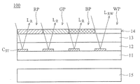
図1Aは、公知の液晶ディスプレイのRGBW四色の画素を有する空間的配置を示す図である。公知のRGBW四色液晶ディスプレイ10は複数の画素領域からなり、それぞれ、赤(RP)、緑(GP)、青(BP)、及び、白(WP)画素領域である。白画素(WP)はカラーフィルターがない。図1Bは、微反射透過型液晶ディスプレイの断面図である。図1B中、微反射透過型液晶ディスプレイ装置100は、液晶ディスプレイパネルアセンブリからなり、ストレージキャパシタCST と薄膜トランジスタ(図示しない)をその上に有する下基板11と、上基板13、及び、上基板13と下基板11間に挟置される液晶層12と、を有する。カラーフィルター14は上基板13上に設置される。バックライトユニット(BLU)15からの環境光の反射により、ディスプレイ装置100は反射画像を提供する。
FIG. 1A is a diagram showing a spatial arrangement having RGBW four-color pixels of a known liquid crystal display. The known RGBW four-color
図2は公知の微反射透過型液晶ディスプレイを示す図である。微反射透過型液晶ディスプレイ装置100は、液晶ディスプレイパネルアセンブリ30、パネルアセンブリ30に連接されるゲートドライバ40とデータドライバ50、各素子を制御する信号コントローラーを含む。
FIG. 2 is a diagram showing a known micro-reflection transmissive liquid crystal display. The slightly reflective / transmissive liquid
液晶ディスプレイパネル30は、その構造が1Bで示され、下基板11、上基板13、及び、その間の液晶層12を含む。液晶ディスプレイパネル30は、複数のディスプレイ信号線G1-Gn と D1-Dm、及び、接続された複数の画素を含む。画素領域全体はマトリクス形式で、図1Aで示される。
The structure of the liquid
ディスプレイ信号線G1-Gnと D1-Dmは下基板11上に設置され、ゲート信号を伝送する複数のゲートラインG1-Gn(又は、スキャン信号)、及び、データ信号を伝送する複数のデータラインD1-Dm伝送データ信号からなる。ゲートラインG1-Gnは、互いが平行で、列方向に延伸し、データラインD1-Dmは、互いが平行で、行方向に延伸する。
The display signal lines G 1 -G n and D 1 -D m are installed on the
各画素は、ディスプレイ信号線G1-GnとD1-Dmに接続されるスイッチ素子Tを有し、スイッチ素子Tに接続される液晶層キャパシタCLCとストレージキャパシタCSを含む。スイッチ素子Tは、例えば、薄膜トランジスタ(TFT)で、下基板11上に提供され、三端子を有し、ゲートラインG1-Gnの一つに連接される制御端と、データラインD1-Dmの一つに連接される入力端と、液晶キャパシタCLC とストレージキャパシタ CSTに連接される出力端と、である。
Each pixel has a switching element T which is connected to the display signal lines G 1 -G n and D 1 -D m, and a liquid crystal layer capacitor C LC and the storage capacitor C S which are connected to the switch element T. The switch element T is, for example, a thin film transistor (TFT), is provided on the
ストレージキャパシタ CSTは液晶キャパシタCLC の補助キャパシタである。ストレージキャパシタ CSTは所定の電圧、例えば、コモン電圧Vcomにより供給される。 The storage capacitor CST is an auxiliary capacitor for the liquid crystal capacitor CLC . The storage capacitor CST is supplied with a predetermined voltage, for example, a common voltage Vcom .
しかし、公知の四色液晶ディスプレイ10は以下のような欠点と困難があり、例えば、反射率と反射コントラスト比(RCR)を改善しなければならない。微反射透過型液晶ディスプレイにとって、バックライトユニットからの反射は外部反射であると定義され、ストレージキャパシタ CST、或いは、金属信号、及び、データラインからの反射は内部反射と定義される。内部反射は微反射透過型液晶ディスプレイにノイズを生成し、反射コントラスト比は減少する。各画素に対応するストレージキャパシタ CSTは内部で環境光を反射し、LRで表示される。白色サブピクセルWPの内部反射LRWはカラーフィルターのブロックが不足なので、白色サブピクセルWPの内部、外部反射共に反射品質を悪化させて、公知の四色液晶ディスプレイは反射コントラスト比を悪化させるので、良好な反射画像を表示することができない。
However, the known four-color
本発明は、RGBW四色サブピクセル領域を有する微反射透過型液晶ディスプレイを提供し、白色画素領域に対応するストレージキャパシタを三色のサブピクセル領域の一つに設置して、上述の問題を解決することを目的とする。 The present invention provides a micro-reflection transmissive liquid crystal display having RGBW four-color sub-pixel areas, and a storage capacitor corresponding to a white pixel area is installed in one of the three-color sub-pixel areas to solve the above-mentioned problem The purpose is to do.
本発明は画像表示システムを提供する。本システムの具体例は液晶ディスプレイパネルを含む。LCDパネルは、三原色サブピクセル領域と白サブピクセル領域のアレイを有する第一基板と、第二基板と、第一基板と第二基板間の液晶層を含む。各サブピクセル領域は、トランジスタと、トランジスタに対応するストレージキャパシタを含む。白サブピクセル領域のトランジスタに対応するストレージキャパシタは、三原色のサブピクセルの一領域内に設置される。 The present invention provides an image display system. Specific examples of the system include a liquid crystal display panel. The LCD panel includes a first substrate having an array of three primary color subpixel regions and a white subpixel region, a second substrate, and a liquid crystal layer between the first substrate and the second substrate. Each sub-pixel region includes a transistor and a storage capacitor corresponding to the transistor. Storage capacitors corresponding to the transistors in the white subpixel region are disposed in one region of the three primary color subpixels.
本発明のもう一つの実施例によると、本発明は画像表示システムを提供し、液晶ディスプレイパネルを含む。LCDパネルは三原色サブピクセル領域、及び、白サブピクセル領域を有する第一基板を含む。各サブピクセル領域は、トランジスタと、トランジスタに対応するストレージキャパシタ、からなる。第二基板は、三原色のサブピクセルに対応する三原色のカラーフィルターを有する。液晶層は第一基板と第二基板間に位置する。三色のカラーフィルターの一領域は、対応するサブピクセル領域の一領域より大きい。よって、白画素のストレージキャパシタは、三原色フィルターの大領域内に配置される。 According to another embodiment of the present invention, the present invention provides an image display system and includes a liquid crystal display panel. The LCD panel includes a first substrate having three primary color subpixel regions and a white subpixel region. Each subpixel region includes a transistor and a storage capacitor corresponding to the transistor. The second substrate has three primary color filters corresponding to the three primary color sub-pixels. The liquid crystal layer is located between the first substrate and the second substrate. One area of the three-color filter is larger than one area of the corresponding sub-pixel area. Therefore, the storage capacitor of the white pixel is arranged in a large area of the three primary color filters.
本発明の長所は、白色画素領域に対応するストレージキャパシタを三色サブピクセル領域の一つに設置して、白色サブピクセル領域に対応するストレージキャパシタが信号干渉を生じるのを防止し、効果的に微反射透過型液晶ディスプレイの反射模式下のノイズ干渉問題を解決し、反射率と反射コントラスト比を改善する。 The advantage of the present invention is that a storage capacitor corresponding to the white pixel region is installed in one of the three color sub-pixel regions to prevent the storage capacitor corresponding to the white sub-pixel region from causing signal interference and effectively. It solves the noise interference problem under the reflection model of the micro-reflection liquid crystal display and improves the reflectance and reflection contrast ratio.
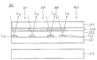
図3は本発明の実施例による微反射透過型液晶ディスプレイの断面図である。微反射透過型液晶ディスプレイ200は四原色のRGBWサブピクセル領域を有する。各サブピクセル領域は、上にストレージキャパシタCSTと薄膜トランジスタ(図示しない)を配置する下基板211、上基板213、下基板211と上基板213間に位置し、誘電異方性を有する液晶層212を含む。白色サブピクセル領域WPに対応するストレージキャパシタCST’は三原色サブピクセルの一つに設置される。例えば、白色サブピクセル領域WPの薄膜トランジスタに対応するストレージキャパシタCST’は、内部反射を阻止できるので、青サブピクセルBP領域内に設置される。
FIG. 3 is a cross-sectional view of a micro-reflection transmissive liquid crystal display according to an embodiment of the present invention. The micro-reflection transmissive
カラーフィルター214は上基板上213に設置される。白色サブピクセル領域WPはフィルターがない。入射光を分極する一対の偏光板(図示しない)が、微反射透過型液晶ディスプレイ200の上下基板211、213の外側表面に設置される。
The
環境光がパネルに入射し、バックライトユニット215から外部反射するので、微反射透過型液晶ディスプレイ200は反射画像を提供することができる。
Since ambient light is incident on the panel and is externally reflected from the
図4は、本発明の実施例による四原色微反射透過型液晶ディスプレイを示す図である。微反射透過型液晶ディスプレイ200は、液晶ディスプレイパネルアセンブリ230と、液晶ディスプレイパネルアセンブリ230に連接されるゲートドライバ240とデータドライバ250と、各素子を制御するコントローラー(図示しない)を含む。
FIG. 4 is a view showing a four-primary-color slightly reflective transmissive liquid crystal display according to an embodiment of the present invention. The micro-reflection transmissive
液晶ディスプレイパネルアセンブリ230は、その構造が図3で示され、下基板211、上基板213、及び、その間に挟置された液晶層212を含む。液晶ディスプレイパネルアセンブリ230は、複数のディスプレイ信号線G1-GnとD1-Dmと、これらに接続されてマトリクスに配置される複数の画素を含む。
The structure of the liquid crystal
ディスプレイ信号線G1-GnとD1-Dmは下基板211上に設置され、ゲート信号を伝送する複数のゲートラインG1-Gn(又は、スキャン信号)、及び、データ信号を伝送する複数のデータラインD1-Dに区分される。ゲートラインG1-Gnは、互いが平行で、列方向に延伸し、データラインD1-Dmは、互いが平行で、行方向に延伸する。 The display signal lines G 1 -G n and D 1 -D m are installed on the lower substrate 211 and transmit a plurality of gate lines G 1 -G n (or scan signals) for transmitting gate signals and data signals. Is divided into a plurality of data lines D 1 -D. The gate lines G 1 -G n are parallel to each other and extend in the column direction, and the data lines D 1 -D m are parallel to each other and extend in the row direction.
各画素は、ディスプレイ信号線G1-Gnと D1-Dmに接続されるスイッチ素子Tと、スイッチ素子Tに接続される液晶キャパシタCLCとストレージキャパシタCSTを含む。 Each pixel includes a switching element T which is connected to the display signal lines G 1 -G n and D 1 -D m, the liquid crystal capacitor C LC and the storage capacitor C ST that are connected to the switch element T.
スイッチ素子Tは、例えば、薄膜トランジスタ(TFT)で、下基板211に提供され、三端子を有し、それぞれ、ゲートラインG1-Gnの一つに連接される制御端と、データラインD1-Dmの一つに連接される入力端と、液晶キャパシタCLC とストレージキャパシタ CSTに連接される出力端と、である。 The switch element T is, for example, a thin film transistor (TFT), which is provided on the lower substrate 211, has three terminals, and is connected to one of the gate lines G 1 -G n and the data line D 1. an input terminal which is connected to one -D m, and an output terminal which is connected to the liquid crystal capacitor C LC and the storage capacitor C ST, is.
液晶キャパシタCLCは、下基板上の画素電極と上基板上のコモン電極とその間の液晶層から構成される。液晶層の作用はキャパシタの誘電層である。画素電極はスイッチ素子Tに連接され、且つ、コモン電極は上基板領域を被覆する。 The liquid crystal capacitor C LC includes a pixel electrode on the lower substrate, a common electrode on the upper substrate, and a liquid crystal layer therebetween. The action of the liquid crystal layer is the dielectric layer of the capacitor. The pixel electrode is connected to the switch element T, and the common electrode covers the upper substrate region.
ストレージキャパシタ CSTは液晶キャパシタCLC の補助キャパシタである。又は、ストレージキャパシタ CSTは、画素電極190と隣接する前ゲートラインと称するゲートラインを有し、絶縁体により画素電極を被覆する。各サブピクセル領域は薄膜トランジスタT、及び、対応するストレージキャパシタ CSTを有する。白色サブピクセル領域WPのトランジスタTに対応するストレージキャパシタ CST’は、三原色サブピクセル領域の一つに設置される。更に特定すると、白色サブピクセルWPの薄膜トランジスタTに対応するストレージキャパシタCST’は青サブピクセル領域BP内に設置される。
The storage capacitor CST is an auxiliary capacitor for the liquid crystal capacitor CLC . Alternatively, the storage capacitor CST has a gate line called a previous gate line adjacent to the
カラーフィルターは内部反射に対する阻止能力が良いので、微反射透過型液晶ディスプレイのノイズを減少させる。特に、白色サブピクセル領域WP内のストレージキャパシタCST’が三原色サブピクセル領域内に設置されるので、ストレージキャパシタCSTからの環境光の内部反射は、カラーフィルターによりブロックされる。 Since the color filter has a good blocking ability against internal reflection, it reduces the noise of the micro-reflection transmissive liquid crystal display. In particular, since the storage capacitor C ST ′ in the white subpixel region WP is installed in the three primary color subpixel regions, the internal reflection of ambient light from the storage capacitor CST is blocked by the color filter.
本発明の実施例による液晶ディスプレイのTFTアレイパネルの詳細構造は以下で説明し、図5と図6を参照する。 The detailed structure of the TFT array panel of the liquid crystal display according to an embodiment of the present invention will be described below and refer to FIGS. 5 and 6.
図5は、本発明の実施例による微反射透過型液晶ディスプレイのTFTアレイ基板の配置図である。図6は図5中のV−V’に沿った断面図である。 FIG. 5 is a layout view of a TFT array substrate of a micro-reflection transmissive liquid crystal display according to an embodiment of the present invention. FIG. 6 is a cross-sectional view taken along V-V ′ in FIG. 5.
ストレージキャパシタ導体177はゲートライン121の延伸部分127を被覆する。本発明の実施例によると、白色サブピクセル領域WPに対応するストレージキャパシタ導体177’は、ゲートライン121の延伸部分127を青色サブピクセル領域BPにおいて被覆する。
The
白色サブピクセル領域WPのトランジスタTに対応するストレージキャパシタCST’が青色サブピクセル領域BP範囲内に設置されるので、環境光の内部反射は、青色フィルターによりブロックされる。これにより、反射画像品質と反射コントラスト比が共に改善される。 Since the storage capacitor C ST ′ corresponding to the transistor T in the white subpixel region WP is disposed within the blue subpixel region BP, internal reflection of ambient light is blocked by the blue filter. This improves both the reflection image quality and the reflection contrast ratio.
更に、本発明のもう一つの実施例は、三原色フィルターの一つを対応するサブピクセル領域より大きく製作し、例えば、青色フィルターが、白色サブピクセル領域WPとの一部を被覆するように形成され、つまり、白色サブピクセル領域WPに対応するストレージキャパシタCST’は、青色フィルターの範囲内に位置する。 Furthermore, another embodiment of the present invention makes one of the three primary color filters larger than the corresponding subpixel region, for example, a blue filter is formed to cover a part with the white subpixel region WP. That is, the storage capacitor C ST ′ corresponding to the white subpixel region WP is located within the blue filter.
図7は本発明のもう一つの実施例による微反射透過型液晶ディスプレイ300の断面図である。三原色フィルターの一つは、白色サブピクセル領域に延伸し、白色サブピクセルWPに対応するストレージキャパシタCSTを被覆する。例えば、青色サブピクセルBP’は、白色サブピクセル領域WP’に延伸して、且つ、ストレージキャパシタCSTを被覆するように製作する。白色サブピクセル領域は、高透過度の透明フィルター、白色フィルター、或いは、無フィルターの一つに対応する。青色フィルターは内部反射を効率よく遮断するので、微反射透過型液晶ディスプレイパネルのノイズは減少し、反射率と反射コントラスト比は改善される。
FIG. 7 is a cross-sectional view of a micro-reflection transmissive
図8Aは青色サブピクセルの配置図で、青カラーフィルターBP’は白色サブピクセル領域WP’に延伸し、ストレージキャパシタCSTを被覆する。図8Bは微反射透過型液晶ディスプレイパネル300の白色サブピクセル領域WP’の配置図である。
FIG. 8A is an arrangement diagram of blue subpixels, and a blue color filter BP ′ extends to a white subpixel region WP ′ and covers a storage capacitor CST . FIG. 8B is a layout view of the white sub-pixel region WP ′ of the micro-reflection transmissive liquid
図9は画像表示システムのもう一つの具体例を示す図で、この場合、本発明の微反射透過型液晶ディスプレイパネル1を含むディスプレイ装置3として実行され、よって、ディスプレイパネル200、300は、図3と図7で示される。微反射透過型液晶ディスプレイパネル1はコントローラー2に結合されて、図9で示されるディスプレイ装置3を構成する。コントローラー2は、ソース、ゲート駆動回路(図示しない)を有し、微反射透過型液晶ディスプレイパネル1を制御して、入力に従って画像を表示する。
FIG. 9 is a diagram showing another specific example of the image display system. In this case, the image display system is executed as the
図10は画像表示システムのもう一つの具体例を示し、この場合、電子装置5として実行し、本発明の微反射透過型液晶ディスプレイパネル1を含むディスプレイ装置を組み込む。入力素子4は、図10で示されるように、ディスプレイ装置3のコントローラー2に結合され、マイクロプロセッサを有し、データをコントローラー2に入力し、画像を表示する。電子装置5は、PDA、携帯電話、ノート型パソコン、タブレットPC、或いは、その他の携帯式電子装置である。
FIG. 10 shows another specific example of the image display system. In this case, the display device is implemented as the
本発明では好ましい実施例を前述の通り開示したが、これらは決して本発明に限定するものではなく、当該技術を熟知する者なら誰でも、本発明の精神と領域を脱しない範囲内で各種の変動や潤色を加えることができ、従って本発明の保護範囲は、特許請求の範囲で指定した内容を基準とする。 In the present invention, preferred embodiments have been disclosed as described above. However, the present invention is not limited to the present invention, and any person who is familiar with the technology can use various methods within the spirit and scope of the present invention. Variations and moist colors can be added, so the protection scope of the present invention is based on what is specified in the claims.
10 公知のRGBW四色液晶ディスプレイ
RP 赤色サブピクセル領域
GP 緑色サブピクセル領域
BP 青色サブピクセル領域
WP 白色サブピクセル領域
100 微反射透過型液晶ディスプレイ装置
11 下基板
12 液晶層
13 上基板
14 カラーフィルター
15 バックライトユニット(BLU)
LR 内部反射
LRW 内部反射
30 液晶ディスプレイパネルアセンブリ
40 ゲートドライバ
50 データドライバ
G1-Gn ゲートライン
D1-Dm データライン
T スイッチ素子
CLC 液晶キャパシタ
CST ストレージキャパシタ
200 微反射透過型液晶ディスプレイ
300 微反射透過型液晶ディスプレイ
RP 赤色サブピクセル領域
GP 緑色サブピクセル領域
BP 青色サブピクセル領域
BP’ 青色サブピクセル領域
WP 青色サブピクセル領域
WP’ 青色サブピクセル領域
211 下基板
311 下基板
212 液晶層
312 液晶層
213 上基板
313 上基板
214 カラーフィルター
314 カラーフィルター
215 バックライトモジュール(BLU)
315 バックライトモジュール(BLU)
LR 内部反射
230 液晶ディスプレイパネル
240 ゲートドライバ
250 データドライバ
G1-Gn ゲートライン
D1-Dm データライン
T スイッチ素子
CLC 液晶キャパシタ
CST バックライトモジュール(BLU)
CST’ ストレージキャパシタ
190 画素電極
177 ストレージキャパシタ導体
177’ ストレージキャパシタ導体
121 ゲートライン
127 延伸部分
1 微反射透過型液晶ディスプレイ
2 コントローラー
3 ディスプレイ装置
4 入力素子
5 電子装置
10 Known RGBW four-color liquid crystal display
RP red sub-pixel area
GP green sub-pixel area
BP Blue subpixel area
WP white sub-pixel area
100 Low reflection transmission type liquid crystal display device
11 Lower board
12 Liquid crystal layer
13 Upper substrate
14 Color filter
15 Backlight unit (BLU)
L R Internal reflection
L RW internal reflection
30 LCD panel assembly
40 Gate driver
50 Data driver
G 1 -G n gate line
D 1 -D m data line
T switch element
C LC liquid crystal capacitor
C ST storage capacitor
200 Low reflection transmission type liquid crystal display
300 Low reflection transmission type liquid crystal display
RP red sub-pixel area
GP green sub-pixel area
BP Blue subpixel area
BP 'Blue subpixel area
WP blue subpixel area
WP 'Blue sub-pixel area
211 Lower board
311 Lower board
212 Liquid crystal layer
312 Liquid crystal layer
213 Upper substrate
313 Upper substrate
214 Color filter
314 Color filter
215 Backlight module (BLU)
315 Backlight module (BLU)
L R Internal reflection
230 LCD panel
240 gate driver
250 Data driver
G 1 -G n gate line
D 1 -D m data line
T switch element
C LC liquid crystal capacitor
C ST backlight module (BLU)
C ST ' storage capacitor
190 pixel electrode
177 Storage capacitor conductor
177 'storage capacitor conductor
121 Gate line
127 stretched part
1 Low reflection transmission type liquid crystal display
2 Controller
3 Display device
4 Input element
5 Electronic equipment
Claims (19)
前期液晶ディスプレイパネルは、
三原色サブピクセル領域と白サブピクセル領域のアレイを有し、各サブピクセル領域がトランジスタと前記トランジスタに対応するストレージキャパシタを有する第一基板、
第二基板、及び
前記第一基板と前記第二基板間の液晶層
を含み、前記白色サブピクセル領域の前記トランジスタに対応する前記ストレージキャパシタは、前記三原色のサブピクセルの一領域内に設置されることを特徴とするシステム。 An image display system including a liquid crystal display panel,
The LCD panel for the previous term
A first substrate having an array of three primary color subpixel regions and a white subpixel region, each subpixel region having a transistor and a storage capacitor corresponding to the transistor;
The storage capacitor corresponding to the transistor in the white subpixel region is disposed in one region of the three primary color subpixels, and includes a second substrate and a liquid crystal layer between the first substrate and the second substrate. A system characterized by that.
前記液晶ディスプレイパネルは、
三原色サブピクセル領域と白サブピクセル領域のアレイを有し、各サブピクセル領域がトランジスタと、前記トランジスタに対応するストレージキャパシタを含む第一基板、
前記三原色画素領域に対応する三カラーフィルターを有する第二基板、及び
前記第一基板と前記第二基板間の液晶層、
を含み、前記三原色フィルターの一つは対応するサブピクセル領域より大きく、これにより、前記白色サブピクセル領域の前記ストレージキャパシタを被覆することを特徴とするシステム。 An image display system including a liquid crystal display panel,
The liquid crystal display panel is
A first substrate having an array of three primary color subpixel regions and a white subpixel region, each subpixel region including a transistor and a storage capacitor corresponding to the transistor;
A second substrate having three color filters corresponding to the three primary color pixel regions, and a liquid crystal layer between the first substrate and the second substrate,
And wherein one of the three primary color filters is larger than a corresponding subpixel area, thereby covering the storage capacitor of the white subpixel area.
Applications Claiming Priority (2)
| Application Number | Priority Date | Filing Date | Title |
|---|---|---|---|
| US11/402,586 | 2006-04-11 | ||
| US11/402,586 US7499116B2 (en) | 2006-04-11 | 2006-04-11 | Systems for displaying images having micro-reflective transmission liquid crystal display with particular storage capacitor arrangement |
Publications (2)
| Publication Number | Publication Date |
|---|---|
| JP2007279719A true JP2007279719A (en) | 2007-10-25 |
| JP4956786B2 JP4956786B2 (en) | 2012-06-20 |
Family
ID=38574826
Family Applications (1)
| Application Number | Title | Priority Date | Filing Date |
|---|---|---|---|
| JP2007080632A Expired - Fee Related JP4956786B2 (en) | 2006-04-11 | 2007-03-27 | Image display system |
Country Status (3)
| Country | Link |
|---|---|
| US (1) | US7499116B2 (en) |
| JP (1) | JP4956786B2 (en) |
| CN (1) | CN101055386B (en) |
Cited By (4)
| Publication number | Priority date | Publication date | Assignee | Title |
|---|---|---|---|---|
| JP2009180961A (en) * | 2008-01-31 | 2009-08-13 | Epson Imaging Devices Corp | Display device |
| US8084939B2 (en) | 2009-02-02 | 2011-12-27 | Samsung Electronics Co., Ltd. | Organic light emitting display and fabricating method thereof |
| JP2012185992A (en) * | 2011-03-04 | 2012-09-27 | Dainippon Printing Co Ltd | Color filter and organic el display device |
| WO2014002982A1 (en) * | 2012-06-28 | 2014-01-03 | 東レ株式会社 | Color filter, and display device |
Families Citing this family (10)
| Publication number | Priority date | Publication date | Assignee | Title |
|---|---|---|---|---|
| US7746294B2 (en) * | 2006-04-14 | 2010-06-29 | University Of Central Florida Research Foundation, Inc. | Transflective liquid crystal display |
| KR101225192B1 (en) * | 2009-11-23 | 2013-01-22 | 에스케이텔레콤 주식회사 | Color electronic paper using RGBW color particles and Driving method of the same |
| TWI390315B (en) | 2009-12-23 | 2013-03-21 | Au Optronics Corp | Pixel array |
| CN102156371B (en) * | 2010-01-15 | 2013-09-25 | 友达光电股份有限公司 | pixel array |
| KR101113345B1 (en) * | 2010-03-24 | 2012-02-29 | 삼성모바일디스플레이주식회사 | Plate panel display device and making method for the same |
| US9165526B2 (en) * | 2012-02-28 | 2015-10-20 | Shenzhen Yunyinggu Technology Co., Ltd. | Subpixel arrangements of displays and method for rendering the same |
| KR102390962B1 (en) | 2015-08-05 | 2022-04-27 | 삼성디스플레이 주식회사 | Display device |
| CN112433561A (en) * | 2018-06-29 | 2021-03-02 | 中兴通讯股份有限公司 | Display screen module, terminal, control method of terminal and computer storage medium |
| US20220352481A1 (en) * | 2019-10-08 | 2022-11-03 | Sharp Kabushiki Kaisha | Light-emitting device |
| KR102741338B1 (en) * | 2020-07-07 | 2024-12-13 | 삼성디스플레이 주식회사 | Display device |
Citations (1)
| Publication number | Priority date | Publication date | Assignee | Title |
|---|---|---|---|---|
| JP2005316416A (en) * | 2004-04-27 | 2005-11-10 | Au Optronics Corp | Liquid crystal panel and liquid crystal display |
Family Cites Families (6)
| Publication number | Priority date | Publication date | Assignee | Title |
|---|---|---|---|---|
| JP4011292B2 (en) * | 2001-01-15 | 2007-11-21 | 株式会社日立製作所 | LIGHT EMITTING ELEMENT AND DISPLAY DEVICE |
| US6816355B2 (en) * | 2001-09-13 | 2004-11-09 | Seiko Epson Corporation | Capacitor, semiconductor device, electro-optic device, method of manufacturing capacitor, method of manufacturing semiconductor device, and electronic apparatus |
| US7365722B2 (en) * | 2002-09-11 | 2008-04-29 | Samsung Electronics Co., Ltd. | Four color liquid crystal display and driving device and method thereof |
| KR100997965B1 (en) * | 2003-09-25 | 2010-12-02 | 삼성전자주식회사 | Liquid crystal display |
| US20060139522A1 (en) * | 2004-12-27 | 2006-06-29 | Toppoly Optoelectronics Corp. | Transflective liquid crystal display device with balanced chromaticity |
| US20070063192A1 (en) * | 2005-09-20 | 2007-03-22 | Toppoly Optoelectronics Corp. | Systems for emitting light incorporating pixel structures of organic light-emitting diodes |
-
2006
- 2006-04-11 US US11/402,586 patent/US7499116B2/en not_active Expired - Fee Related
-
2007
- 2007-03-26 CN CN2007100900344A patent/CN101055386B/en not_active Expired - Fee Related
- 2007-03-27 JP JP2007080632A patent/JP4956786B2/en not_active Expired - Fee Related
Patent Citations (1)
| Publication number | Priority date | Publication date | Assignee | Title |
|---|---|---|---|---|
| JP2005316416A (en) * | 2004-04-27 | 2005-11-10 | Au Optronics Corp | Liquid crystal panel and liquid crystal display |
Cited By (6)
| Publication number | Priority date | Publication date | Assignee | Title |
|---|---|---|---|---|
| JP2009180961A (en) * | 2008-01-31 | 2009-08-13 | Epson Imaging Devices Corp | Display device |
| US8674904B2 (en) | 2008-01-31 | 2014-03-18 | Japan Display West Inc. | Color display device with a non-rectangle display |
| US8084939B2 (en) | 2009-02-02 | 2011-12-27 | Samsung Electronics Co., Ltd. | Organic light emitting display and fabricating method thereof |
| JP2012185992A (en) * | 2011-03-04 | 2012-09-27 | Dainippon Printing Co Ltd | Color filter and organic el display device |
| WO2014002982A1 (en) * | 2012-06-28 | 2014-01-03 | 東レ株式会社 | Color filter, and display device |
| JPWO2014002982A1 (en) * | 2012-06-28 | 2016-06-02 | 東レ株式会社 | Color filter and display device |
Also Published As
| Publication number | Publication date |
|---|---|
| JP4956786B2 (en) | 2012-06-20 |
| US7499116B2 (en) | 2009-03-03 |
| US20070236621A1 (en) | 2007-10-11 |
| CN101055386B (en) | 2010-05-26 |
| CN101055386A (en) | 2007-10-17 |
Similar Documents
| Publication | Publication Date | Title |
|---|---|---|
| JP4956786B2 (en) | Image display system | |
| US7561239B2 (en) | Liquid crystal device and electronic apparatus | |
| CN101408702B (en) | Liquid crystal display device | |
| JP4111180B2 (en) | Liquid crystal display device and electronic device | |
| JP4717672B2 (en) | Liquid crystal device and electronic device | |
| US7477347B2 (en) | Liquid crystal device and electronic apparatus | |
| JP4167085B2 (en) | Liquid crystal display | |
| JP4607158B2 (en) | Liquid crystal display device and electronic device | |
| JPH11295717A (en) | Liquid crystal display | |
| CN100520505C (en) | Four-color liquid crystal display | |
| KR20180049297A (en) | Liquid Crystal Display Having Light Valve | |
| US20060139527A1 (en) | Liquid crystal display device with transmission and reflective display modes and method of displaying balanced chromaticity image for the same | |
| JP2006139058A (en) | Liquid crystal display device and electronic device | |
| JP2007148347A (en) | Liquid crystal display device and terminal using the same | |
| JP2007058007A (en) | Liquid crystal device and electronic apparatus | |
| JP2009075421A (en) | Liquid crystal device and electronic equipment | |
| JP2007094089A (en) | Electrooptical device and electronic equipment | |
| CN100476540C (en) | Electro-optical device and electronic apparatus | |
| JP2007139948A (en) | Electro-optical device and electronic apparatus | |
| JP5076781B2 (en) | Transmission type liquid crystal display device and electronic apparatus | |
| JP2008180929A (en) | Liquid crystal display device and driving method of the same | |
| JP2008233312A (en) | Liquid crystal device and electronic equipment | |
| JP2013054385A (en) | Liquid crystal display device | |
| JP2008070734A (en) | Liquid crystal display and electronic equipment | |
| JP2007121326A (en) | Electrooptical device and electronic appliance |
Legal Events
| Date | Code | Title | Description |
|---|---|---|---|
| A621 | Written request for application examination |
Free format text: JAPANESE INTERMEDIATE CODE: A621 Effective date: 20100315 |
|
| A977 | Report on retrieval |
Free format text: JAPANESE INTERMEDIATE CODE: A971007 Effective date: 20120125 |
|
| TRDD | Decision of grant or rejection written | ||
| A01 | Written decision to grant a patent or to grant a registration (utility model) |
Free format text: JAPANESE INTERMEDIATE CODE: A01 Effective date: 20120131 |
|
| A01 | Written decision to grant a patent or to grant a registration (utility model) |
Free format text: JAPANESE INTERMEDIATE CODE: A01 |
|
| A711 | Notification of change in applicant |
Free format text: JAPANESE INTERMEDIATE CODE: A712 Effective date: 20120227 |
|
| A61 | First payment of annual fees (during grant procedure) |
Free format text: JAPANESE INTERMEDIATE CODE: A61 Effective date: 20120227 |
|
| FPAY | Renewal fee payment (event date is renewal date of database) |
Free format text: PAYMENT UNTIL: 20150330 Year of fee payment: 3 |
|
| R150 | Certificate of patent or registration of utility model |
Free format text: JAPANESE INTERMEDIATE CODE: R150 |
|
| R250 | Receipt of annual fees |
Free format text: JAPANESE INTERMEDIATE CODE: R250 |
|
| R250 | Receipt of annual fees |
Free format text: JAPANESE INTERMEDIATE CODE: R250 |
|
| R250 | Receipt of annual fees |
Free format text: JAPANESE INTERMEDIATE CODE: R250 |
|
| LAPS | Cancellation because of no payment of annual fees |