KR101113345B1 - Plate panel display device and making method for the same - Google Patents
Plate panel display device and making method for the same Download PDFInfo
- Publication number
- KR101113345B1 KR101113345B1 KR1020100026262A KR20100026262A KR101113345B1 KR 101113345 B1 KR101113345 B1 KR 101113345B1 KR 1020100026262 A KR1020100026262 A KR 1020100026262A KR 20100026262 A KR20100026262 A KR 20100026262A KR 101113345 B1 KR101113345 B1 KR 101113345B1
- Authority
- KR
- South Korea
- Prior art keywords
- pixels
- pixel
- white
- blue
- green
- Prior art date
- Legal status (The legal status is an assumption and is not a legal conclusion. Google has not performed a legal analysis and makes no representation as to the accuracy of the status listed.)
- Expired - Fee Related
Links
Images


Classifications
-
- G—PHYSICS
- G09—EDUCATION; CRYPTOGRAPHY; DISPLAY; ADVERTISING; SEALS
- G09G—ARRANGEMENTS OR CIRCUITS FOR CONTROL OF INDICATING DEVICES USING STATIC MEANS TO PRESENT VARIABLE INFORMATION
- G09G3/00—Control arrangements or circuits, of interest only in connection with visual indicators other than cathode-ray tubes
- G09G3/20—Control arrangements or circuits, of interest only in connection with visual indicators other than cathode-ray tubes for presentation of an assembly of a number of characters, e.g. a page, by composing the assembly by combination of individual elements arranged in a matrix no fixed position being assigned to or needed to be assigned to the individual characters or partial characters
- G09G3/22—Control arrangements or circuits, of interest only in connection with visual indicators other than cathode-ray tubes for presentation of an assembly of a number of characters, e.g. a page, by composing the assembly by combination of individual elements arranged in a matrix no fixed position being assigned to or needed to be assigned to the individual characters or partial characters using controlled light sources
- G09G3/30—Control arrangements or circuits, of interest only in connection with visual indicators other than cathode-ray tubes for presentation of an assembly of a number of characters, e.g. a page, by composing the assembly by combination of individual elements arranged in a matrix no fixed position being assigned to or needed to be assigned to the individual characters or partial characters using controlled light sources using electroluminescent panels
- G09G3/32—Control arrangements or circuits, of interest only in connection with visual indicators other than cathode-ray tubes for presentation of an assembly of a number of characters, e.g. a page, by composing the assembly by combination of individual elements arranged in a matrix no fixed position being assigned to or needed to be assigned to the individual characters or partial characters using controlled light sources using electroluminescent panels semiconductive, e.g. using light-emitting diodes [LED]
- G09G3/3208—Control arrangements or circuits, of interest only in connection with visual indicators other than cathode-ray tubes for presentation of an assembly of a number of characters, e.g. a page, by composing the assembly by combination of individual elements arranged in a matrix no fixed position being assigned to or needed to be assigned to the individual characters or partial characters using controlled light sources using electroluminescent panels semiconductive, e.g. using light-emitting diodes [LED] organic, e.g. using organic light-emitting diodes [OLED]
-
- H—ELECTRICITY
- H10—SEMICONDUCTOR DEVICES; ELECTRIC SOLID-STATE DEVICES NOT OTHERWISE PROVIDED FOR
- H10K—ORGANIC ELECTRIC SOLID-STATE DEVICES
- H10K59/00—Integrated devices, or assemblies of multiple devices, comprising at least one organic light-emitting element covered by group H10K50/00
- H10K59/10—OLED displays
- H10K59/12—Active-matrix OLED [AMOLED] displays
- H10K59/121—Active-matrix OLED [AMOLED] displays characterised by the geometry or disposition of pixel elements
- H10K59/1216—Active-matrix OLED [AMOLED] displays characterised by the geometry or disposition of pixel elements the pixel elements being capacitors
-
- G—PHYSICS
- G09—EDUCATION; CRYPTOGRAPHY; DISPLAY; ADVERTISING; SEALS
- G09G—ARRANGEMENTS OR CIRCUITS FOR CONTROL OF INDICATING DEVICES USING STATIC MEANS TO PRESENT VARIABLE INFORMATION
- G09G2300/00—Aspects of the constitution of display devices
- G09G2300/04—Structural and physical details of display devices
- G09G2300/0439—Pixel structures
- G09G2300/0452—Details of colour pixel setup, e.g. pixel composed of a red, a blue and two green components
-
- G—PHYSICS
- G09—EDUCATION; CRYPTOGRAPHY; DISPLAY; ADVERTISING; SEALS
- G09G—ARRANGEMENTS OR CIRCUITS FOR CONTROL OF INDICATING DEVICES USING STATIC MEANS TO PRESENT VARIABLE INFORMATION
- G09G2300/00—Aspects of the constitution of display devices
- G09G2300/04—Structural and physical details of display devices
- G09G2300/0439—Pixel structures
- G09G2300/0465—Improved aperture ratio, e.g. by size reduction of the pixel circuit, e.g. for improving the pixel density or the maximum displayable luminance or brightness
-
- G—PHYSICS
- G09—EDUCATION; CRYPTOGRAPHY; DISPLAY; ADVERTISING; SEALS
- G09G—ARRANGEMENTS OR CIRCUITS FOR CONTROL OF INDICATING DEVICES USING STATIC MEANS TO PRESENT VARIABLE INFORMATION
- G09G2320/00—Control of display operating conditions
- G09G2320/02—Improving the quality of display appearance
- G09G2320/0233—Improving the luminance or brightness uniformity across the screen
-
- H—ELECTRICITY
- H10—SEMICONDUCTOR DEVICES; ELECTRIC SOLID-STATE DEVICES NOT OTHERWISE PROVIDED FOR
- H10K—ORGANIC ELECTRIC SOLID-STATE DEVICES
- H10K59/00—Integrated devices, or assemblies of multiple devices, comprising at least one organic light-emitting element covered by group H10K50/00
- H10K59/30—Devices specially adapted for multicolour light emission
- H10K59/35—Devices specially adapted for multicolour light emission comprising red-green-blue [RGB] subpixels
- H10K59/351—Devices specially adapted for multicolour light emission comprising red-green-blue [RGB] subpixels comprising more than three subpixels, e.g. red-green-blue-white [RGBW]
Landscapes
- Engineering & Computer Science (AREA)
- Physics & Mathematics (AREA)
- Computer Hardware Design (AREA)
- General Physics & Mathematics (AREA)
- Theoretical Computer Science (AREA)
- Geometry (AREA)
- Microelectronics & Electronic Packaging (AREA)
- Liquid Crystal (AREA)
- Devices For Indicating Variable Information By Combining Individual Elements (AREA)
- Electroluminescent Light Sources (AREA)
Abstract
본 발명의 목적은 백색 발란스를 맞추며 휘도 특성이 떨어지지 않는 평판 표시장치 및 그의 제조방법을 제공하는 것이다.
본 발명은 상기 목적을 달성하기 위하여 본 발명의 제 1 측면은, 복수의 주사선과, 상기 복수의 주사선과 교차되게 형성된 복수의 데이터선과, 상기 복수의 주사선과 복수의 데이터선에 각각 연결되며, 적색, 녹색, 청색 및 백색 화소를 포함하는 화소부; 상기 데이터선으로 데이터 신호를 출력하는 데이터 구동부; 및 상기 주사선으로 주사신호를 출력하는 주사구동부를 포함하되, 상기 청색 화소의 스토리지 캐패시터는 상기 백색화소의 화소전극 하부에 에 형성되는 평판 표시장치 및 그의 제조방법을 제공하는 것이다. SUMMARY OF THE INVENTION An object of the present invention is to provide a flat panel display and a method of manufacturing the same, in which white balance is achieved and luminance characteristics are not degraded.
In order to achieve the above object, the present invention provides a first aspect of the present invention, a plurality of scan lines, a plurality of data lines formed to intersect the plurality of scan lines, and a plurality of scan lines and a plurality of data lines, respectively, A pixel unit including green, blue, and white pixels; A data driver for outputting a data signal to the data line; And a scan driver for outputting a scan signal to the scan line, wherein the storage capacitor of the blue pixel is formed under the pixel electrode of the white pixel, and a manufacturing method thereof.
Description
본 발명은 평판 표시장치 및 그의 제조방법에 관한 것으로, 더욱 상세히 설명하면, 색좌표가 일치되도록 하는 평판 표시장치 및 그의 제조방법을 제공하는 것이다.
The present invention relates to a flat panel display and a method for manufacturing the same, and more particularly, to provide a flat panel display and a method for manufacturing the same so that the color coordinates match.
최근, 음극선관(Cathode Ray Tube)의 단점인 무게와 부피를 줄일 수 있는 각종 평판 표시장치들이 개발되고 있다. 평판 표시장치로는 액정 표시장치(Liquid Crystal Display), 전계방출 표시장치(Field Emission Display), 플라즈마 표시패널(Plasma Display Panel) 및 유기전계발광표시장치(Organic Light Emitting Display) 등이 있다. Recently, various flat panel displays have been developed to reduce weight and volume, which are disadvantages of cathode ray tubes. The flat panel display includes a liquid crystal display, a field emission display, a plasma display panel, and an organic light emitting display.
상기의 평판 표시장치는 수동 매트릭스(passive matrix) 방식과 능동 매트릭스(active matrix) 방식으로 구분되며, 수동 매트릭스 방식에 비해 해상도 및 동영상 구현 능력이 우수한 능동 매트릭스 방식이 주로 사용되고 있다. The flat panel display device is classified into a passive matrix method and an active matrix method, and an active matrix method having an excellent resolution and a video implementation capability is mainly used as compared to the passive matrix method.
능동 매트릭스 방식의 평판 표시 장치는 신호를 전달하기 위한 박막 트랜지스터 및 신호를 유지시키기 위한 스토리지 캐패시터를 포함한다. An active matrix flat panel display includes a thin film transistor for transmitting a signal and a storage capacitor for holding a signal.
하지만, 상기의 스토리지 캐패시터에 의해 화소의 개구율이 낮아지는 문제점이 있다. 특히, 청색 화소의 경우 다른 적색, 녹색의 화소보다 낮은 휘도 특성을 갖고 있어 개구율이 작아지면 다른 색의 화소보다 더 낮은 휘도 특성을 갖는다. However, there is a problem that the aperture ratio of the pixel is lowered by the storage capacitor. In particular, the blue pixel has a lower luminance characteristic than other red and green pixels, and when the aperture ratio is small, the blue pixel has a lower luminance characteristic than other colored pixels.
또한, 화소의 휘도를 높이기 위해 적색, 녹색, 청색의 화소 이외에 백색 화소를 더 구비하도록 할 수 있는데, 이러한 경우 적색, 녹색 및 청색으로 인해 표현되는 백색과 백색 화소로 인해 표현되는 백색은 색좌표가 일치하지 않게 된다. 따라서, 색 표현이 잘못될 수 있는 문제점이 있다.
In addition, in order to increase the luminance of the pixel, a white pixel may be further provided in addition to the red, green, and blue pixels. In this case, the white color represented by the white pixels and the white color represented by the red, green, and blue colors coincide with each other. You will not. Therefore, there is a problem that the color representation may be wrong.
본 발명의 목적은 백색 발란스를 맞추며 휘도 특성이 떨어지지 않는 평판 표시장치 및 그의 제조방법을 제공하는 것이다. SUMMARY OF THE INVENTION An object of the present invention is to provide a flat panel display and a method of manufacturing the same, in which white balance is achieved and luminance characteristics are not degraded.
상기 목적을 달성하기 위하여 본 발명의 제 1 측면은, 복수의 주사선과, 상기 복수의 주사선과 교차되게 형성된 복수의 데이터선과, 상기 복수의 주사선과 복수의 데이터선에 각각 연결되며, 적색, 녹색, 청색 및 백색 화소를 포함하는 화소부; 상기 데이터선으로 데이터 신호를 출력하는 데이터 구동부; 및 상기 주사선으로 주사신호를 출력하는 주사구동부를 포함하되, 상기 청색 화소의 스토리지 캐패시터는 상기 백색화소의 화소전극 하부에 형성되는 평판 표시장치를 제공하는 것이다. In order to achieve the above object, a first aspect of the present invention provides a plurality of scan lines, a plurality of data lines formed to intersect the plurality of scan lines, and a plurality of scan lines and a plurality of data lines, respectively. A pixel unit including blue and white pixels; A data driver for outputting a data signal to the data line; And a scan driver for outputting a scan signal to the scan line, wherein the storage capacitor of the blue pixel is formed under the pixel electrode of the white pixel.
상기 목적을 달성하기 위하여 본 발명의 제 2 측면은, 복수의 주사선과, 상기 복수의 주사선과 교차하는 복수의 데이터선과, 상기 복수의 주사선과 복수의 데이터선이 교차하는 화소영역에 각각 형성되는, 적색, 녹색, 청색 및 백색 화소를 포함하는 평판표시장치의 제조방법에 있어서, 기판 상에 도전층을 형성하여 상기 적색, 녹색, 청색 및 백색 화소의 게이트 전극과 스토리지 캐패시터의 제 1 전극을 형성하되, 상기 청색 화소의 스토리지 캐패시터의 제 1 전극은 상기 백색 화소가 위치하는 상기 화소영역에 형성되는 단계; 및 상기 게이트 전극과 상기 스토리지 캐패시터의 제 1 전극의 상부에 절연막을 형성하고, 그 상부에 소스 드레인 메탈을 이용하여 소스, 드레인 전극과 상기 스토리지 캐패시터의 제 2 전극을 형성하는 단계를 포함하는 평판표시장치의 제조방법을 제공하는 것이다. In order to achieve the above object, the second aspect of the present invention provides a plurality of scan lines, a plurality of data lines intersecting the plurality of scan lines, and a plurality of data lines intersecting the plurality of scan lines, respectively. A method of manufacturing a flat panel display device including red, green, blue, and white pixels, wherein a conductive layer is formed on a substrate to form gate electrodes of the red, green, blue, and white pixels and first electrodes of a storage capacitor. Forming a first electrode of the storage capacitor of the blue pixel in the pixel area in which the white pixel is located; And forming an insulating layer on the gate electrode and the first electrode of the storage capacitor, and forming a source, a drain electrode, and a second electrode of the storage capacitor using a source drain metal on the gate electrode. It is to provide a method of manufacturing the device.
본 발명에 따른 평판 표시장치 및 그의 제조방법에 의하면, 백색 화소의 개구율이 낮아지고 청색화소의 개구율이 높아지게 됨으로 인해 적색, 녹색 및 청색으로 생성하는 백색의 색좌표와 백색 화소로 생성하는 백색의 색좌표가 일치하게 된다. According to the flat panel display and the manufacturing method thereof according to the present invention, since the aperture ratio of the white pixel is lowered and the aperture ratio of the blue pixel is increased, the white color coordinates generated by the red, green, and blue colors and the white color coordinates generated by the white pixels are reduced. Will match.
도 1은 본 발명에 따른 평판 표시장치의 구조를 나타내는 구조도이다.
도 2는 본 발명에 따른 화소부에 채용된 화소의 구조를 나타내는 평면도이다.
도 3은 평판 표시장치의 색좌표를 나타내는 그래프이다.
도 4a 내지 도 4f는 본 발명에 따른 평판 표시 장치의 제조 방법을 설명하기 위한 단면도이다. 1 is a structural diagram showing a structure of a flat panel display device according to the present invention.
2 is a plan view showing the structure of a pixel employed in the pixel portion according to the present invention.
3 is a graph illustrating color coordinates of a flat panel display.
4A to 4F are cross-sectional views illustrating a method of manufacturing a flat panel display device according to the present invention.
이하, 본 발명의 실시예를 첨부한 도면을 참조하여 설명하면 다음과 같다. Hereinafter, an embodiment of the present invention will be described with reference to the accompanying drawings.
도 1은 본 발명에 따른 평판 표시장치의 구조를 나타내는 구조도이다. 도 1을 참조하여 설명하면, 평판 표시장치는 화소부(100), 데이터구동부(120), 주사구동부(130)를 포함한다. 1 is a structural diagram showing a structure of a flat panel display device according to the present invention. Referring to FIG. 1, the flat panel display device includes a
화소부(100)는 데이터선(D1, D2,....Dm-1, Dm)과 주사선(S1,S2,...Sn-1,Sn)이 교차하는 영역에 복수의 화소(101R,101G,101B,101W)가 형성되고 복수의 화소(101R,101G,101B,101W) 트랜지스터와 상기 트랜지스터와 연결된 화소전극을 포함한다. 이때, 첫번째 열은 적색화소(101R), 녹색화소(101G), 청색화소(101B), 백색화소(101W)의 순서로 배열되고 두번째 열은 청색화소(101B), 백색화소(101W), 적색화소(101R), 녹색화소(101G)의 순으로 배열된다. 그리고, 세번째 열은 다시 적색화소(101R), 녹색화소(101G), 청색화소(101B), 백색화소(101W)의 순서로 배열되며, 이러한 반복은 계속된다. 그리고, 각각의 화소의 개구율은 청색화소(101B)의 개구율이 가장 크고 백색 화소(101W)의 개구율이 가장 작다. 또한, 적색화소(101R), 녹색화소(101G)의 화소의 개구율의 크기는 동일하다고 판단할 수 있다. The
데이터구동부(120)는 데이터신호를 생성하는 수단으로, 영상신호를 이용하여 데이터신호를 생성한다. 그리고, 데이터구동부(120)는 화소부(100)의 데이터선(D1, D2,....Dm-1, Dm)과 연결되어 생성된 데이터 신호를 화소부(100)에 인가한다. The data driver 120 is a means for generating a data signal. The data driver 120 generates a data signal using an image signal. The data driver 120 applies the data signal generated by being connected to the data lines D1, D2,... Dm-1, Dm of the
주사구동부(130)는 주사신호를 생성하는 수단으로, 주사선(S1,S2,...Sn-1,Sn)에 연결되어 주사신호를 화소부(100)의 특정한 행에 전달한다. 주사신호가 전달된 화소(101)에는 데이터구동부(120)에서 출력된 데이터신호가 전달되어 데이터신호의 전압이 화소에 전달되게 된다.
The scan driver 130 is a means for generating a scan signal. The scan driver 130 is connected to the scan lines S1, S2,..., Sn-1, Sn to transfer the scan signal to a specific row of the
도 2는 본 발명에 따른 화소부에 채용된 화소의 구조를 나타내는 평면도이다. 도 2를 참조하여 설명하면, 화소부(100)는 각각의 데이터선(Dk-2,Dk-1Dk,Dk+1)과 주사선(Sj)이 교차하는 영역에 적색화소(101R), 녹색화소(101G), 청색화소(101B), 백색화소(101W)가 배열된다. 2 is a plan view showing the structure of a pixel employed in the pixel portion according to the present invention. Referring to FIG. 2, the
각각의 화소는 데이터신호를 유지하기 위한 스토리지 캐패시터가 포함되어 있다. 본 발명에서는 적색 및 녹색화소의 스토리지 캐패시터(R.scap,G.scap)는 각각 적색,화소(101R), 녹색 화소(101G)의 개구부에 형성된다. 그리고, 청색 화소(101B)의 스토리지 캐패시터(B.scap)는 백색 화소(101W)의 개구부에 형성된다. 또한, 백색 화소(101W)의 스토리지 캐패시터(B.scap)는 자신의 화소인 백색 화소(101W)의 개구부에 형성된다. 즉, 백색 화소(101W)의 개구부에는 청색 화소(101B)의 스토리지 캐패시터(B.caps)와 자신의 스토리지 캐패시터인 백색 화소(101W)의 스토리지 캐패시터(B.scap)가 형성된다. Each pixel includes a storage capacitor for holding a data signal. In the present invention, the storage capacitors R. scap and G. scap of the red and green pixels are formed in the openings of the red,
따라서, 스토리지 캐패시터(B.scap)에 의해 청색 화소(101B)의 개구율은 다른 화소들보다 더 크고 백색 화소(101W)의 개구율은 가장 작게 형성된다. Therefore, the opening ratio of the
그리고, 청색화소(101B)의 스토리지 캐패시터(B.scap)가 청색화소(101B)의 트랜지스터의 게이트와 연결되도록 하기 위해 청색화소의 트랜지스터의 게이트와 백색 화소에 형성되어 있는 청색화소(101B)의 스토리지 캐패시터(B.scap)가 트랜지스터의 게이트까지 연장되어 전기적으로 연결된다.
In addition, the storage capacitor B.scap of the
도 3은 평판 표시장치의 색좌표를 나타내는 그래프이다. 도 3을 참조하여 설명하면, 도 2에 도시된 평판표시장치는 백색를 표현하기 위해서는 적색, 녹색 및 청색의 화소의 휘도를 조절하여 백색를 표현하는 방법과 백색 화소의 휘도에 의해 백색이 표현하는 방법이 있다. 3 is a graph illustrating color coordinates of a flat panel display. Referring to FIG. 3, in the flat panel display of FIG. 2, in order to express white, a method of expressing white by adjusting luminance of red, green, and blue pixels and a method of expressing white by the brightness of white pixels are provided. have.
하지만, 적색, 녹색 및 청색의 화소의 휘도를 조절하여 표현되는 백색과 백색 화소의 휘도에 의해 표현되는 백색의 색좌표가 일치하지 않게 된다. (도 3에서 색도 R+G+B와 색도 W의 위치가 다른 지점에 있는 것이 이를 나타낸다.)However, the color coordinates of white expressed by the luminance of the white pixel and the white expressed by adjusting the luminance of the red, green, and blue pixels do not coincide. (In Fig. 3, the positions of chromaticity R + G + B and chromaticity W are at different points.)
이러한 문제점을 해결하기 위해 백색 화소의 개구율을 줄이도록 하는 방법이 있다. In order to solve this problem, there is a method of reducing the aperture ratio of the white pixel.
백색 화소의 개구율을 줄이기 위한 방법으로 백색 화소의 상부에 블랙매트릭스를 형성하도록 하는 것이 있다. 하지만, 백색 화소의 상부에 블랙매트릭스를 형성하도록 하면 백색 화소의 휘도가 떨어져 전체적으로 휘도가 떨어지게 되는 문제점이 있다. As a method for reducing the aperture ratio of the white pixel, a black matrix is formed on the white pixel. However, when the black matrix is formed on the white pixel, the luminance of the white pixel is lowered and the luminance is generally lowered.
하지만, 본 발명과 같이 청색 화소의 스토리지 캐패시터를 백색 화소에 형성하게 되면 백색 화소의 개구율은 낮아지게 되지만 청색 화소의 개구율은 커지게 된다. 따라서, 백색 화소의 휘도는 낮아지지만 상대적으로 청색화소의 휘도가 높아지기 때문에 전체적인 휘도는 낮아지지 않는다. 따라서, 상기의 문제점을 해결할 수 있다. However, when the storage capacitor of the blue pixel is formed in the white pixel as in the present invention, the aperture ratio of the white pixel is lowered but the aperture ratio of the blue pixel is increased. Therefore, although the luminance of the white pixel is lowered, the luminance of the blue pixel is relatively higher, so that the overall luminance is not lowered. Therefore, the above problem can be solved.
그리고, 적색, 녹색 및 청색의 화소로 생성하는 백색과 백색 화소로 생성하는 백색의 색좌표가 일치하게 되어 백색 발란스를 맞출 수 있다.
Then, the white color coordinates generated by the red, green, and blue pixels and the white color coordinates of the white pixels are coincident to match the white balance.
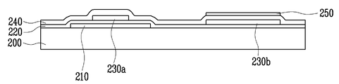
도 4a 내지 도 4f는 본 발명에 따른 평판 표시 장치의 제조 방법을 설명하기 위한 단면도로서, 도 2의 구조를 예로 들어 설명한다. 4A to 4F are cross-sectional views illustrating a method of manufacturing a flat panel display device according to an exemplary embodiment of the present invention.
기판(200) 상에 활성층(210)을 형성하고 제 1 절연막(220)을 형성한다(도 4a). 그리고, 제 1 절연막(220)의 상부에 제 1 도전층을 형성하고 패터닝하여 활성층 상부에는 게이트 전극(230a)을 형성하고 기판 상(200)에는 스토리지 캐패시터의 제 1 전극(230b)을 형성한다(도 4b). 도 4b에는 도시되어 있는 제 1 도전층에 의해 주사선이 형성되며 게이트 전극과 연결된다. 이때, 스토리지 캐패시터의 제 1 전극(230b) 중 청색 화소의 스토리지 캐패시터의 제 1 전극(230b)은 백색 화소의 개구부에 형성된다. 즉, 청색 화소에 형성되는 제 1 도전층은 게이트 전극과 배선이 형성되고 백색 화소에 형성되는 제 1 도전층은 게이트 전극과 청색화소의 스토리지 캐패시터의 제 1 전극과 백색 화소의 스토리지 캐패시터의 제 2 전극이 형성되며 청색화소에 형성된 배선이 백색 화소에 형성된 청색 화소의 스토리지 캐패시터와 연결되도록 한다. An
그리고, 그 상부에 제 2 절연막(240)을 형성한 후 스토리지 캐패시터의 제 1 전극(230b)에 대향되는 위치에 스토리지 캐패시터의 제 2 전극(250)을 형성한다(도 4c). 따라서, 청색 화소의 스토리지 캐패시터의 제 2 전극은 백색 화소 영역에 형성된다. 그리고, 그 상부에 제 3 절연막(260)을 형성한다(도 4d). After forming the second insulating
그리고, 제 1 내지 제 3 컨텍홀(300a 내지 300c)을 형성하고 소스 드레인 메탈을 형성함으로써 제 1 컨텍홀 내지 제 3 컨텍홀(300a 내지 300c)을 통해 소스 드레인 메탈이 활성층(210)과 스토리지 캐패시터의 제 2 전극(240c)과 전기적으로 접촉하게 된다. 그리고, 그 상부에 제 4 절연막(280)을 형성한다(도 4e). 이때, 제 1 컨텍홀(300a)을 통해 활성층(210)과 연결된 소스 드레인 메탈(270a)은 박막트랜지스터의 소스 전극으로 형성되고 제 2 컨텍홀(300b)을 통해 활성층(210)과 연결된 소스 드레인 메탈(270b)은 박막트랜지스터의 드레인 전극으로 형성된다. 또한, 제 3 컨텍홀(300c)을 통해 스토리지 캐패시터의 제 2 전극과 연결된 소스 드레인 메탈(270b)은 박막트랜지스터의 드레인 전극과 연결됨으로써 트랜지스터를 통해 전달되는 신호가 스토리지 캐패시터로 전달될 수 있도록 한다. In addition, the source drain metal is formed through the first contact hole through the
그리고, 평탄화층(290)을 형성한 후 소스 드레인 메탈과 접촉하도록 하는 제 4 컨텍홀(300d)을 형성한 후 화소전극(300)을 형성한다(도 4f). 따라서, 화소전극(300)은 제 4 컨텍홀(300d)을 통해 소스 드레인 메탈(270b)과 접촉함으로써 박막트랜지스터를 통해 전달되는 신호를 전달받는다.
After forming the
본 발명의 바람직한 실시예가 특정 용어들을 사용하여 기술되어 왔지만, 그러한 기술은 단지 설명을 하기 위한 것이며, 다음의 청구범위의 기술적 사상 및 범위로부터 이탈되지 않고 여러 가지 변경 및 변화가 가해질 수 있는 것으로 이해되어져야 한다. While preferred embodiments of the present invention have been described using specific terms, such descriptions are for illustrative purposes only and it is understood that various changes and modifications may be made without departing from the spirit and scope of the following claims. You must lose.
100: 화소부 120: 데이터구동부
130: 주사구동부 101R: 적색화소
101G: 녹색화소 101B: 청색화소
101W: 백색화소 B.scap: 스토리지 캐패시터100: pixel portion 120: data driver
130: scanning drive 101R: red pixel
101G:
101W: White Pixel B.scap: Storage Capacitor
Claims (8)
상기 데이터선으로 데이터 신호를 출력하는 데이터 구동부; 및
상기 주사선으로 주사신호를 출력하는 주사구동부를 포함하며,
상기 적색, 녹색 및 백색 화소에 스토리지 캐패시터가 각각 구비되고,
상기 청색 화소의 스토리지 캐패시터는 상기 백색 화소에 구비된 평판 표시장치.
A pixel portion connected to the plurality of scan lines, the plurality of data lines formed to intersect the plurality of scan lines, and the plurality of scan lines and the plurality of data lines, respectively, and including red, green, blue, and white pixels;
A data driver for outputting a data signal to the data line; And
A scan driver for outputting a scan signal to the scan line;
Storage capacitors are provided in the red, green, and white pixels, respectively.
The storage capacitor of the blue pixel is provided in the white pixel.
상기 복수의 화소는 상기 주사선 연장 방향으로 상기 적색 화소, 녹색 화소, 청색 화소 및 백색 화소가 순차적으로 배열되고, 상기 데이터선 연장 방향으로 2가지 색의 화소가 교대로 배열되는 것을 특징으로 하는 평판 표시장치.
The method of claim 1,
In the plurality of pixels, the red pixels, the green pixels, the blue pixels, and the white pixels are sequentially arranged in the scanning line extending direction, and two colors of pixels are alternately arranged in the data line extending direction. Device.
순차적으로 배열되고, 상기 주사선 연장 방향 및 상기 데이터선 연장 방향으로 동일한 색의 화소가 연속되지 않도록 배열되는 것을 특징으로 하는 평판 표시장치.
The method of claim 1,
And arranged in a sequential manner so that pixels of the same color are not contiguous in the scanning line extending direction and the data line extending direction.
상기 백색 화소의 개구율이 적색, 녹색 및 청색 화소의 개구율보다 작게 형성되는 평판 표시장치.
The method of claim 1,
And the aperture ratio of the white pixel is smaller than that of the red, green, and blue pixels.
기판 상에 도전층을 형성한 후 패터닝하여 상기 적색, 녹색 및 백색 화소의 스토리지 캐패시터의 제 1 전극을 형성하되, 상기 청색 화소의 스토리지 캐패시터의 제 1 전극은 상기 백색 화소가 위치하는 상기 화소영역에 형성하는 단계;
상기 스토리지 캐패시터의 제 1 전극의 상부에 절연막을 형성하고, 그 상부에 상기 스토리지 캐패시터의 제 2 전극을 형성하는 단계를 포함하는 평판표시장치의 제조방법.
A flat panel display device comprising a plurality of scan lines, a plurality of data lines intersecting the plurality of scan lines, and red, green, blue, and white pixels respectively formed in pixel regions where the plurality of scan lines and the plurality of data lines intersect. In the manufacturing method of
After forming a conductive layer on a substrate, patterning is performed to form a first electrode of the storage capacitor of the red, green, and white pixels, wherein the first electrode of the storage capacitor of the blue pixel is in the pixel region where the white pixel is located. Forming;
Forming an insulating layer on the first electrode of the storage capacitor and forming a second electrode of the storage capacitor on the first electrode of the storage capacitor.
상기 복수의 화소는 상기 주사선 연장 방향으로 상기 적색 화소, 녹색 화소, 청색 화소 및 백색 화소가 순차적으로 배열되고, 상기 데이터선 연장 방향으로 2가지 색의 화소가 교대로 배열되는 것을 특징으로 하는 평판표시장치의 제조방법.
The method of claim 5, wherein
The plurality of pixels may include the red pixels, the green pixels, the blue pixels, and the white pixels sequentially arranged in the scanning line extending direction, and two colors of pixels may be alternately arranged in the data line extending direction. Method of manufacturing the device.
순차적으로 배열되고, 상기 주사선 연장 방향 및 상기 데이터선 연장 방향으로 동일한 색의 화소가 연속되지 않도록 배열되는 것을 특징으로 하는 평판표시장치의 제조방법.
The method according to claim 6,
And sequentially arranged so that pixels of the same color are not contiguous in the scanning line extending direction and the data line extending direction.
상기 백색 화소의 개구율이 적색, 녹색 및 청색 화소의 개구율보다 작게 형성되는 평판표시장치의 제조방법. The method according to claim 6,
And an aperture ratio of the white pixel is smaller than an aperture ratio of red, green, and blue pixels.
Priority Applications (4)
| Application Number | Priority Date | Filing Date | Title |
|---|---|---|---|
| KR1020100026262A KR101113345B1 (en) | 2010-03-24 | 2010-03-24 | Plate panel display device and making method for the same |
| US13/034,612 US8988242B2 (en) | 2010-03-24 | 2011-02-24 | Flat panel display device and method for manufacturing thereof |
| CN201110065549.5A CN102201189B (en) | 2010-03-24 | 2011-03-11 | Flat panel display device and method for manufacturing thereof |
| EP11159587A EP2369572A1 (en) | 2010-03-24 | 2011-03-24 | Flat panel display device and method of manufacture |
Applications Claiming Priority (1)
| Application Number | Priority Date | Filing Date | Title |
|---|---|---|---|
| KR1020100026262A KR101113345B1 (en) | 2010-03-24 | 2010-03-24 | Plate panel display device and making method for the same |
Publications (2)
| Publication Number | Publication Date |
|---|---|
| KR20110107091A KR20110107091A (en) | 2011-09-30 |
| KR101113345B1 true KR101113345B1 (en) | 2012-02-29 |
Family
ID=44063144
Family Applications (1)
| Application Number | Title | Priority Date | Filing Date |
|---|---|---|---|
| KR1020100026262A Expired - Fee Related KR101113345B1 (en) | 2010-03-24 | 2010-03-24 | Plate panel display device and making method for the same |
Country Status (4)
| Country | Link |
|---|---|
| US (1) | US8988242B2 (en) |
| EP (1) | EP2369572A1 (en) |
| KR (1) | KR101113345B1 (en) |
| CN (1) | CN102201189B (en) |
Families Citing this family (8)
| Publication number | Priority date | Publication date | Assignee | Title |
|---|---|---|---|---|
| JP5701139B2 (en) | 2011-04-21 | 2015-04-15 | 株式会社ジャパンディスプレイ | Display device |
| JP6057647B2 (en) * | 2012-09-27 | 2017-01-11 | 三菱電機株式会社 | Display device |
| JP6274771B2 (en) * | 2013-07-26 | 2018-02-07 | 株式会社ジャパンディスプレイ | Light emitting element display device |
| KR102273497B1 (en) * | 2014-12-24 | 2021-07-07 | 엘지디스플레이 주식회사 | Display device and driving method thereof |
| TWI560495B (en) * | 2016-01-28 | 2016-12-01 | Au Optronics Corp | Display apparatus and display control method thereof |
| CN110890408B (en) | 2019-11-28 | 2022-08-19 | 京东方科技集团股份有限公司 | Display panel and display device |
| KR102838285B1 (en) * | 2019-12-31 | 2025-07-23 | 엘지디스플레이 주식회사 | Display device |
| CN116261366A (en) * | 2023-02-22 | 2023-06-13 | 武汉天马微电子有限公司 | Display panel and display device |
Citations (2)
| Publication number | Priority date | Publication date | Assignee | Title |
|---|---|---|---|---|
| JPH0651348A (en) * | 1992-06-01 | 1994-02-25 | Samsung Electron Co Ltd | Liquid crystal display device and manufacture thereof |
| KR100583128B1 (en) * | 2004-06-25 | 2006-05-23 | 삼성에스디아이 주식회사 | Flat panel display with static electricity protection circuit |
Family Cites Families (11)
| Publication number | Priority date | Publication date | Assignee | Title |
|---|---|---|---|---|
| US7012588B2 (en) * | 2001-06-05 | 2006-03-14 | Eastman Kodak Company | Method for saving power in an organic electroluminescent display using white light emitting elements |
| CN1220968C (en) | 2002-02-04 | 2005-09-28 | 凌巨科技股份有限公司 | LCD pixel signal line module |
| KR100997965B1 (en) * | 2003-09-25 | 2010-12-02 | 삼성전자주식회사 | Liquid crystal display |
| KR101067555B1 (en) * | 2004-03-25 | 2011-09-27 | 엘지디스플레이 주식회사 | LCD Display |
| US7382384B2 (en) * | 2004-12-07 | 2008-06-03 | Eastman Kodak Company | OLED displays with varying sized pixels |
| TWI249970B (en) * | 2005-01-12 | 2006-02-21 | Delta Optoelectronics Inc | Method for driving pixel of active display and system thereof |
| KR100725506B1 (en) | 2005-06-13 | 2007-06-08 | 삼성전자주식회사 | Correction method of white balance for display device |
| KR100740221B1 (en) * | 2005-06-29 | 2007-07-18 | 삼성전자주식회사 | Manufacturing method and white balance adjustment device of LCD without aging process |
| US20070063192A1 (en) * | 2005-09-20 | 2007-03-22 | Toppoly Optoelectronics Corp. | Systems for emitting light incorporating pixel structures of organic light-emitting diodes |
| US7499116B2 (en) * | 2006-04-11 | 2009-03-03 | Tpo Displays Corp. | Systems for displaying images having micro-reflective transmission liquid crystal display with particular storage capacitor arrangement |
| US7804525B2 (en) * | 2006-08-24 | 2010-09-28 | Micron Technology, Inc. | Method, apparatus, and system for selecting pixels for automatic white balance processing |
-
2010
- 2010-03-24 KR KR1020100026262A patent/KR101113345B1/en not_active Expired - Fee Related
-
2011
- 2011-02-24 US US13/034,612 patent/US8988242B2/en active Active
- 2011-03-11 CN CN201110065549.5A patent/CN102201189B/en active Active
- 2011-03-24 EP EP11159587A patent/EP2369572A1/en not_active Withdrawn
Patent Citations (2)
| Publication number | Priority date | Publication date | Assignee | Title |
|---|---|---|---|---|
| JPH0651348A (en) * | 1992-06-01 | 1994-02-25 | Samsung Electron Co Ltd | Liquid crystal display device and manufacture thereof |
| KR100583128B1 (en) * | 2004-06-25 | 2006-05-23 | 삼성에스디아이 주식회사 | Flat panel display with static electricity protection circuit |
Also Published As
| Publication number | Publication date |
|---|---|
| KR20110107091A (en) | 2011-09-30 |
| US8988242B2 (en) | 2015-03-24 |
| CN102201189A (en) | 2011-09-28 |
| CN102201189B (en) | 2015-03-11 |
| EP2369572A1 (en) | 2011-09-28 |
| US20110234646A1 (en) | 2011-09-29 |
Similar Documents
| Publication | Publication Date | Title |
|---|---|---|
| KR101113345B1 (en) | Plate panel display device and making method for the same | |
| US11005064B2 (en) | Transparent display substrate and driving method thereof and transparent display device | |
| US11935467B2 (en) | OLED display panel and display device | |
| US9219087B2 (en) | Display, display drive method, method of manufacturing display, and electronic apparatus | |
| CN104078000B (en) | Display and electronic apparatus | |
| US11069756B2 (en) | Display panel, display device and method for driving display panel | |
| US11563059B2 (en) | Display substrate having auxiliary electrode layer electrically connected to first electrode display apparatus, and method of fabricating display substrate | |
| US20150206477A1 (en) | Array substrate, driving method thereof, and display device | |
| US11081538B2 (en) | Organic light emitting diode display device having a circuit structure buried in a substrate thereof | |
| US11538426B2 (en) | Display panel and electronic apparatus | |
| WO2023016341A1 (en) | Display substrate and preparation method therefor, and display apparatus | |
| TW201703248A (en) | Pixel structure and manufacturing method thereof | |
| CN116234382A (en) | Display substrate, display panel and display device | |
| WO2021013181A1 (en) | Array substrate, display panel and display device | |
| US12406628B2 (en) | Display panel and display apparatus | |
| WO2020191870A1 (en) | Display panel and electronic apparatus | |
| KR20200080487A (en) | Organic light emitting diode display device | |
| US20240078978A1 (en) | Display substrate, method for manufacturing the same, and display device | |
| US10706783B2 (en) | Compensation sub-pixel unit, methods of fabricating and driving the same, and pixel structure and display panel using the same | |
| CN111710698A (en) | OLED display panel and manufacturing method thereof | |
| US11551610B2 (en) | Display and driving method | |
| TW202434077A (en) | Light emitting display device | |
| KR102242982B1 (en) | Organic light emitting diode device and method for fabricating the same | |
| CN117715467A (en) | Display panel, preparation method thereof and display device | |
| WO2022267556A1 (en) | Display substrate and preparation method therefor, and display apparatus |
Legal Events
| Date | Code | Title | Description |
|---|---|---|---|
| A201 | Request for examination | ||
| PA0109 | Patent application |
St.27 status event code: A-0-1-A10-A12-nap-PA0109 |
|
| PA0201 | Request for examination |
St.27 status event code: A-1-2-D10-D11-exm-PA0201 |
|
| E902 | Notification of reason for refusal | ||
| PE0902 | Notice of grounds for rejection |
St.27 status event code: A-1-2-D10-D21-exm-PE0902 |
|
| P11-X000 | Amendment of application requested |
St.27 status event code: A-2-2-P10-P11-nap-X000 |
|
| P13-X000 | Application amended |
St.27 status event code: A-2-2-P10-P13-nap-X000 |
|
| PG1501 | Laying open of application |
St.27 status event code: A-1-1-Q10-Q12-nap-PG1501 |
|
| E701 | Decision to grant or registration of patent right | ||
| PE0701 | Decision of registration |
St.27 status event code: A-1-2-D10-D22-exm-PE0701 |
|
| GRNT | Written decision to grant | ||
| PR0701 | Registration of establishment |
St.27 status event code: A-2-4-F10-F11-exm-PR0701 |
|
| PR1002 | Payment of registration fee |
St.27 status event code: A-2-2-U10-U11-oth-PR1002 Fee payment year number: 1 |
|
| PG1601 | Publication of registration |
St.27 status event code: A-4-4-Q10-Q13-nap-PG1601 |
|
| PN2301 | Change of applicant |
St.27 status event code: A-5-5-R10-R11-asn-PN2301 |
|
| PN2301 | Change of applicant |
St.27 status event code: A-5-5-R10-R14-asn-PN2301 |
|
| FPAY | Annual fee payment |
Payment date: 20141231 Year of fee payment: 4 |
|
| PR1001 | Payment of annual fee |
St.27 status event code: A-4-4-U10-U11-oth-PR1001 Fee payment year number: 4 |
|
| R18-X000 | Changes to party contact information recorded |
St.27 status event code: A-5-5-R10-R18-oth-X000 |
|
| FPAY | Annual fee payment |
Payment date: 20151230 Year of fee payment: 5 |
|
| PR1001 | Payment of annual fee |
St.27 status event code: A-4-4-U10-U11-oth-PR1001 Fee payment year number: 5 |
|
| FPAY | Annual fee payment |
Payment date: 20170102 Year of fee payment: 6 |
|
| PR1001 | Payment of annual fee |
St.27 status event code: A-4-4-U10-U11-oth-PR1001 Fee payment year number: 6 |
|
| FPAY | Annual fee payment |
Payment date: 20180102 Year of fee payment: 7 |
|
| PR1001 | Payment of annual fee |
St.27 status event code: A-4-4-U10-U11-oth-PR1001 Fee payment year number: 7 |
|
| FPAY | Annual fee payment |
Payment date: 20190102 Year of fee payment: 8 |
|
| PR1001 | Payment of annual fee |
St.27 status event code: A-4-4-U10-U11-oth-PR1001 Fee payment year number: 8 |
|
| FPAY | Annual fee payment |
Payment date: 20191223 Year of fee payment: 9 |
|
| PR1001 | Payment of annual fee |
St.27 status event code: A-4-4-U10-U11-oth-PR1001 Fee payment year number: 9 |
|
| PR1001 | Payment of annual fee |
St.27 status event code: A-4-4-U10-U11-oth-PR1001 Fee payment year number: 10 |
|
| PR1001 | Payment of annual fee |
St.27 status event code: A-4-4-U10-U11-oth-PR1001 Fee payment year number: 11 |
|
| PR1001 | Payment of annual fee |
St.27 status event code: A-4-4-U10-U11-oth-PR1001 Fee payment year number: 12 |
|
| PR1001 | Payment of annual fee |
St.27 status event code: A-4-4-U10-U11-oth-PR1001 Fee payment year number: 13 |
|
| PC1903 | Unpaid annual fee |
St.27 status event code: A-4-4-U10-U13-oth-PC1903 Not in force date: 20250201 Payment event data comment text: Termination Category : DEFAULT_OF_REGISTRATION_FEE |
|
| H13 | Ip right lapsed |
Free format text: ST27 STATUS EVENT CODE: N-4-6-H10-H13-OTH-PC1903 (AS PROVIDED BY THE NATIONAL OFFICE); TERMINATION CATEGORY : DEFAULT_OF_REGISTRATION_FEE Effective date: 20250201 |
|
| PC1903 | Unpaid annual fee |
St.27 status event code: N-4-6-H10-H13-oth-PC1903 Ip right cessation event data comment text: Termination Category : DEFAULT_OF_REGISTRATION_FEE Not in force date: 20250201 |