JP2007058177A - Liquid crystal display device, driving method of liquid crystal display device, and charge share circuit - Google Patents
Liquid crystal display device, driving method of liquid crystal display device, and charge share circuit Download PDFInfo
- Publication number
- JP2007058177A JP2007058177A JP2006176752A JP2006176752A JP2007058177A JP 2007058177 A JP2007058177 A JP 2007058177A JP 2006176752 A JP2006176752 A JP 2006176752A JP 2006176752 A JP2006176752 A JP 2006176752A JP 2007058177 A JP2007058177 A JP 2007058177A
- Authority
- JP
- Japan
- Prior art keywords
- liquid crystal
- data
- display device
- crystal display
- crystal cell
- Prior art date
- Legal status (The legal status is an assumption and is not a legal conclusion. Google has not performed a legal analysis and makes no representation as to the accuracy of the status listed.)
- Pending
Links
Images


Classifications
-
- G—PHYSICS
- G09—EDUCATION; CRYPTOGRAPHY; DISPLAY; ADVERTISING; SEALS
- G09G—ARRANGEMENTS OR CIRCUITS FOR CONTROL OF INDICATING DEVICES USING STATIC MEANS TO PRESENT VARIABLE INFORMATION
- G09G3/00—Control arrangements or circuits, of interest only in connection with visual indicators other than cathode-ray tubes
- G09G3/20—Control arrangements or circuits, of interest only in connection with visual indicators other than cathode-ray tubes for presentation of an assembly of a number of characters, e.g. a page, by composing the assembly by combination of individual elements arranged in a matrix no fixed position being assigned to or needed to be assigned to the individual characters or partial characters
- G09G3/34—Control arrangements or circuits, of interest only in connection with visual indicators other than cathode-ray tubes for presentation of an assembly of a number of characters, e.g. a page, by composing the assembly by combination of individual elements arranged in a matrix no fixed position being assigned to or needed to be assigned to the individual characters or partial characters by control of light from an independent source
- G09G3/36—Control arrangements or circuits, of interest only in connection with visual indicators other than cathode-ray tubes for presentation of an assembly of a number of characters, e.g. a page, by composing the assembly by combination of individual elements arranged in a matrix no fixed position being assigned to or needed to be assigned to the individual characters or partial characters by control of light from an independent source using liquid crystals
- G09G3/3611—Control of matrices with row and column drivers
- G09G3/3685—Details of drivers for data electrodes
- G09G3/3688—Details of drivers for data electrodes suitable for active matrices only
-
- G—PHYSICS
- G09—EDUCATION; CRYPTOGRAPHY; DISPLAY; ADVERTISING; SEALS
- G09G—ARRANGEMENTS OR CIRCUITS FOR CONTROL OF INDICATING DEVICES USING STATIC MEANS TO PRESENT VARIABLE INFORMATION
- G09G3/00—Control arrangements or circuits, of interest only in connection with visual indicators other than cathode-ray tubes
- G09G3/20—Control arrangements or circuits, of interest only in connection with visual indicators other than cathode-ray tubes for presentation of an assembly of a number of characters, e.g. a page, by composing the assembly by combination of individual elements arranged in a matrix no fixed position being assigned to or needed to be assigned to the individual characters or partial characters
- G09G3/34—Control arrangements or circuits, of interest only in connection with visual indicators other than cathode-ray tubes for presentation of an assembly of a number of characters, e.g. a page, by composing the assembly by combination of individual elements arranged in a matrix no fixed position being assigned to or needed to be assigned to the individual characters or partial characters by control of light from an independent source
- G09G3/36—Control arrangements or circuits, of interest only in connection with visual indicators other than cathode-ray tubes for presentation of an assembly of a number of characters, e.g. a page, by composing the assembly by combination of individual elements arranged in a matrix no fixed position being assigned to or needed to be assigned to the individual characters or partial characters by control of light from an independent source using liquid crystals
- G09G3/3611—Control of matrices with row and column drivers
- G09G3/3685—Details of drivers for data electrodes
-
- G—PHYSICS
- G02—OPTICS
- G02F—OPTICAL DEVICES OR ARRANGEMENTS FOR THE CONTROL OF LIGHT BY MODIFICATION OF THE OPTICAL PROPERTIES OF THE MEDIA OF THE ELEMENTS INVOLVED THEREIN; NON-LINEAR OPTICS; FREQUENCY-CHANGING OF LIGHT; OPTICAL LOGIC ELEMENTS; OPTICAL ANALOGUE/DIGITAL CONVERTERS
- G02F1/00—Devices or arrangements for the control of the intensity, colour, phase, polarisation or direction of light arriving from an independent light source, e.g. switching, gating or modulating; Non-linear optics
- G02F1/01—Devices or arrangements for the control of the intensity, colour, phase, polarisation or direction of light arriving from an independent light source, e.g. switching, gating or modulating; Non-linear optics for the control of the intensity, phase, polarisation or colour
- G02F1/13—Devices or arrangements for the control of the intensity, colour, phase, polarisation or direction of light arriving from an independent light source, e.g. switching, gating or modulating; Non-linear optics for the control of the intensity, phase, polarisation or colour based on liquid crystals, e.g. single liquid crystal display cells
- G02F1/133—Constructional arrangements; Operation of liquid crystal cells; Circuit arrangements
-
- G—PHYSICS
- G09—EDUCATION; CRYPTOGRAPHY; DISPLAY; ADVERTISING; SEALS
- G09G—ARRANGEMENTS OR CIRCUITS FOR CONTROL OF INDICATING DEVICES USING STATIC MEANS TO PRESENT VARIABLE INFORMATION
- G09G3/00—Control arrangements or circuits, of interest only in connection with visual indicators other than cathode-ray tubes
- G09G3/20—Control arrangements or circuits, of interest only in connection with visual indicators other than cathode-ray tubes for presentation of an assembly of a number of characters, e.g. a page, by composing the assembly by combination of individual elements arranged in a matrix no fixed position being assigned to or needed to be assigned to the individual characters or partial characters
-
- G—PHYSICS
- G09—EDUCATION; CRYPTOGRAPHY; DISPLAY; ADVERTISING; SEALS
- G09G—ARRANGEMENTS OR CIRCUITS FOR CONTROL OF INDICATING DEVICES USING STATIC MEANS TO PRESENT VARIABLE INFORMATION
- G09G2310/00—Command of the display device
- G09G2310/02—Addressing, scanning or driving the display screen or processing steps related thereto
- G09G2310/0243—Details of the generation of driving signals
- G09G2310/0248—Precharge or discharge of column electrodes before or after applying exact column voltages
-
- G—PHYSICS
- G09—EDUCATION; CRYPTOGRAPHY; DISPLAY; ADVERTISING; SEALS
- G09G—ARRANGEMENTS OR CIRCUITS FOR CONTROL OF INDICATING DEVICES USING STATIC MEANS TO PRESENT VARIABLE INFORMATION
- G09G2320/00—Control of display operating conditions
- G09G2320/02—Improving the quality of display appearance
- G09G2320/0223—Compensation for problems related to R-C delay and attenuation in electrodes of matrix panels, e.g. in gate electrodes or on-substrate video signal electrodes
-
- G—PHYSICS
- G09—EDUCATION; CRYPTOGRAPHY; DISPLAY; ADVERTISING; SEALS
- G09G—ARRANGEMENTS OR CIRCUITS FOR CONTROL OF INDICATING DEVICES USING STATIC MEANS TO PRESENT VARIABLE INFORMATION
- G09G2330/00—Aspects of power supply; Aspects of display protection and defect management
- G09G2330/02—Details of power systems and of start or stop of display operation
- G09G2330/021—Power management, e.g. power saving
- G09G2330/023—Power management, e.g. power saving using energy recovery or conservation
-
- G—PHYSICS
- G09—EDUCATION; CRYPTOGRAPHY; DISPLAY; ADVERTISING; SEALS
- G09G—ARRANGEMENTS OR CIRCUITS FOR CONTROL OF INDICATING DEVICES USING STATIC MEANS TO PRESENT VARIABLE INFORMATION
- G09G3/00—Control arrangements or circuits, of interest only in connection with visual indicators other than cathode-ray tubes
- G09G3/20—Control arrangements or circuits, of interest only in connection with visual indicators other than cathode-ray tubes for presentation of an assembly of a number of characters, e.g. a page, by composing the assembly by combination of individual elements arranged in a matrix no fixed position being assigned to or needed to be assigned to the individual characters or partial characters
- G09G3/34—Control arrangements or circuits, of interest only in connection with visual indicators other than cathode-ray tubes for presentation of an assembly of a number of characters, e.g. a page, by composing the assembly by combination of individual elements arranged in a matrix no fixed position being assigned to or needed to be assigned to the individual characters or partial characters by control of light from an independent source
- G09G3/36—Control arrangements or circuits, of interest only in connection with visual indicators other than cathode-ray tubes for presentation of an assembly of a number of characters, e.g. a page, by composing the assembly by combination of individual elements arranged in a matrix no fixed position being assigned to or needed to be assigned to the individual characters or partial characters by control of light from an independent source using liquid crystals
- G09G3/3611—Control of matrices with row and column drivers
- G09G3/3614—Control of polarity reversal in general
Landscapes
- Engineering & Computer Science (AREA)
- Physics & Mathematics (AREA)
- General Physics & Mathematics (AREA)
- Theoretical Computer Science (AREA)
- Computer Hardware Design (AREA)
- Crystallography & Structural Chemistry (AREA)
- Chemical & Material Sciences (AREA)
- Nonlinear Science (AREA)
- Mathematical Physics (AREA)
- Optics & Photonics (AREA)
- Control Of Indicators Other Than Cathode Ray Tubes (AREA)
- Liquid Crystal Display Device Control (AREA)
- Liquid Crystal (AREA)
Abstract
【課題】本発明は、チャージシェアリングの效果を極大化し、消費電流を減少させると共にデータ集積回路の発熱を減少させることができる液晶表示装置とその駆動方法に関する。
【解決手段】本液晶表示装置は、複数のゲートラインと複数のデータラインとがそれぞれ交差し、液晶セルClcが複数配列された液晶セルアレイと、液晶セルアレイの一端側の外方に配置され、データラインにデータ電圧が充電される前に、データラインをプリチャージするための第1のチャージシェア回路106と、液晶セルアレイの他端側の外方に配置され、データラインにデータ電圧が充電される前に、データラインをプリチャージするための第2のチャージシェア回路105を備えることを特徴とする液晶表示装置。
【選択図】図8
The present invention relates to a liquid crystal display device capable of maximizing the effect of charge sharing, reducing current consumption, and reducing heat generation of a data integrated circuit, and a driving method thereof.
The liquid crystal display device includes a liquid crystal cell array in which a plurality of gate lines and a plurality of data lines intersect, a plurality of liquid crystal cells Clc are arranged, and an outer side of one end side of the liquid crystal cell array. Before the data voltage is charged to the line, the first charge share circuit 106 for precharging the data line is disposed outside the other end of the liquid crystal cell array, and the data line is charged with the data voltage. A liquid crystal display device comprising a second charge share circuit 105 for precharging a data line before.
[Selection] Figure 8
Description
本発明は、液晶表示装置に関し、特に、消費電流を減少させると共にデータ集積回路の発熱を減少させることができる液晶表示装置、その駆動方法及びチャージシェア回路に関する。 The present invention relates to a liquid crystal display device, and more particularly to a liquid crystal display device that can reduce current consumption and heat generation of a data integrated circuit, a driving method thereof, and a charge share circuit.
一般に、液晶表示装置は、軽量、薄型、低消費電力駆動などの特徴を有し、その応用の範囲が広がっている。そのため、液晶表示装置は、OA機器、オーディオ/ビデオ機器などに利用されている。このような液晶表示装置は、マトリックス状に配列された複数の制御用スイッチング素子に印加される信号によって光ビームの透過量を調節し、画面に所望の画像を表示している。スイッチング素子としては、薄膜トランジスタ(Thin Film Transistor、以下、“TFT”という)が主に利用されている。 In general, a liquid crystal display device has features such as light weight, thinness, and low power consumption driving, and its application range is widened. Therefore, liquid crystal display devices are used for OA equipment, audio / video equipment, and the like. Such a liquid crystal display device displays a desired image on a screen by adjusting the amount of transmission of a light beam by signals applied to a plurality of control switching elements arranged in a matrix. As the switching element, a thin film transistor (hereinafter referred to as “TFT”) is mainly used.
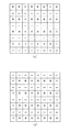
図1は、従来の液晶表示装置を概略的に示す図面である。
図1を参照すると、従来の液晶表示装置は、データライン(D1〜Dm)とゲートライン(G1〜Gn)とがそれぞれ交差し、その交差部に液晶セルClcを駆動するためのTFTが形成された液晶パネル14と、液晶パネル14のデータライン(D1〜Dm)にビデオ信号を供給するためのデータ駆動回路12と、液晶パネル14のゲートライン(G1〜Gn)にスキャンパルスを供給するためのゲート駆動回路13と、データ駆動回路12及びゲート駆動回路13を制御するためのタイミングコントローラ11とを備える。
FIG. 1 schematically illustrates a conventional liquid crystal display device.
Referring to FIG. 1, in the conventional liquid crystal display device, data lines (D1 to Dm) and gate lines (G1 to Gn) intersect with each other, and TFTs for driving the liquid crystal cell Clc are formed at the intersections. The
液晶パネル14は、2枚のガラス基板の間に液晶が注入されて形成され、その下部ガラス基板上には、データライン(D1〜Dm)とゲートライン(G1〜Gn)とが互いに直交して形成される。データライン(D1〜Dm)とゲートライン(G1〜Gn)とのそれぞれの交差部に形成されたTFTは、ゲートライン(G1〜Gn)からのスキャンパルスに応じて、データライン(D1〜Dm)のビデオ信号を液晶セルClcに供給する。そこで、TFTのゲート電極は、ゲートライン(G1〜Gn)に接続され、TFTのソース電極は、データライン(D1〜Dm)に接続される。TFTのドレーン電極は、液晶セルClcの画素電極に接続される。画素電極と対向する共通電極には、共通電圧Vcomが供給される。
The
そして、液晶パネル14の各液晶セルClcには、液晶セルClcに充電された電圧を一定に維持するためのストレージキャパシターCstが形成される。このストレージキャパシターCstは、n番目のゲートラインに接続された液晶セルClcとn−1番目の前段のゲートラインとの間に形成されてもよいし、n番目のゲートラインに接続された液晶セルClcと別の共通ストレージラインとの間に形成されてもよい。
In each liquid crystal cell Clc of the
データ駆動回路12は、所定のチャンネル数を有する複数のデータ集積回路を含む。ここで、データ集積回路は、クロックをサンプリングするためのシフトレジスタ、データを一時保存するためのレジスタ、シフトレジスタからのクロック信号に応じて、データを1ライン分ずつ保存し、保存された1ライン分のデータを同時に出力するためのラッチ、ラッチからのデータ値に対応して、正極性/負極性のガンマ電圧を選択するためのデジタル−アナログ変換器、正極性/負極性のガンマ電圧によって変換されたアナログデータ(ビデオ信号)が供給されるデータライン(D1〜Dm)を選択するためのマルチプレクサ、及びマルチプレクサと選択されたデータラインとの間に接続された出力バッファなどから構成される。このようなデータ集積回路は、タイミングコントローラ11の制御下で、データライン(D1〜Dm)にビデオ信号を供給する。
The
ゲート駆動回路13は、スキャンパルスを順次発生するシフトレジスタと、スキャンパルスの電圧を液晶セルClcの駆動に適したレベルにシフトさせるためのレベルシフタなどで構成される。このゲート駆動回路13は、タイミングコントローラ11の制御下で、ゲートライン(G1〜Gn)に、ビデオ信号に同期するスキャンパルスを順次供給する。
The
タイミングコントローラ11は、垂直/水平同期信号V、HとクロックCLKとを用いて、ゲート駆動回路13を制御するためのゲート制御信号GDCと、データ駆動回路12を制御するためのデータ制御信号DDCとを発生する。データ制御信号DDCは、ソーススタートパルス(Source Start Pulse:SSP)、ソースシフトクロック(Source Shift Clock:SSC)、ソース出力信号(Source Output Enable:SOE)、極性信号(Polarity:POL)などを含む。ゲート制御信号GDCは、ゲートシフトクロック(Gate Shift Clock:GSC)、ゲート出力信号(Gate Output Enable:GOE)、ゲートスタートパルス(Gate Start Pulse:GSP)などを含む。
The
このような液晶表示装置では、液晶パネル14の液晶セルClcを駆動するために、フレームインバージョン方式(Frame Inversion Method)、ラインインバージョン方式(Line Inversion Method)、コラムインバージョン方式(Column Inversion Method)、及びドットインバージョン方式(Dot Inversion Method)のようなインバージョン駆動方法が使用される。
In such a liquid crystal display device, in order to drive the liquid crystal cell Clc of the
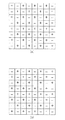
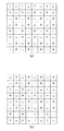
図2は、フレームインバージョン方式を、図3は、ラインインバージョン方式を、図4は、コラムインバージョン方式を、図5は、1ドットインバージョン方式を、図6は、2ドットインバージョン方式を示す。図2〜図6における(a)と(b)とは、液晶セルの全てのフレームに供給されるビデオ信号の極性を示し、「+」は、液晶セルに供給される正極性のビデオ信号を、「−」は、液晶セルに供給される負極性のビデオ信号を示す。 2 shows a frame inversion method, FIG. 3 shows a line inversion method, FIG. 4 shows a column inversion method, FIG. 5 shows a 1-dot inversion method, and FIG. 6 shows a 2-dot inversion method. Indicates. 2 to 6, (a) and (b) indicate the polarities of the video signals supplied to all the frames of the liquid crystal cell, and “+” indicates the positive video signals supplied to the liquid crystal cells. , “−” Indicates a negative video signal supplied to the liquid crystal cell.
しかし、このようなインバージョン駆動方式では、ビデオ信号の極性が反転されることから、消費電流が増加し、また、データ集積回路の発熱が増加する問題点がある。特に、1水平周期または2水平周期ごとにビデオ信号の極性が反転される1ドット及び2ドットインバージョン駆動方式では、このような問題がさらに深刻化される。このような問題点を解決するために、チャージシェアリング(Charge Sharing)を用いて、データライン(D1〜Dm)をプリチャージ(Pre−Chargeing)し、電圧のスイング幅を減らす方案が提示されている。 However, such an inversion driving method has problems that the polarity of the video signal is inverted, resulting in an increase in current consumption and an increase in heat generation of the data integrated circuit. In particular, in the one-dot and two-dot inversion driving method in which the polarity of the video signal is inverted every horizontal cycle or every two horizontal cycles, such a problem becomes more serious. In order to solve such a problem, a method for reducing the voltage swing width by pre-charging the data lines (D1 to Dm) using charge sharing is proposed. Yes.
しかし、従来のチャージシェアリングでは、チャージシェア回路に隣接した部分のデータラインにおいては、図7aに示されているように、完全にチャージシェアリング(Charge Sharing)が実行されるが、チャージシェア回路から遠くなるほど、RC遅延によって、図7bに示されているように、チャージシェアリングの效果が減少する短所がある。特に、現在、大型パネルを実現するための研究が進んでいるが、大型のパネルを製作する場合、大型化による負荷(Load)の増加によって、パネルの末端では、チャージシェアリングの效果がさらに減少する問題がある。 However, in the conventional charge sharing, as shown in FIG. 7a, charge sharing is completely performed on the data line adjacent to the charge sharing circuit. As shown in FIG. 7b, the effect of charge sharing decreases due to the RC delay. In particular, research to realize a large panel is currently underway. However, when a large panel is manufactured, the effect of charge sharing is further reduced at the end of the panel due to an increase in load due to an increase in size. There is a problem to do.
従って、本発明の目的は、消費電流を減少させると共にデータ集積回路の発熱を減少させることができる液晶表示装置、その駆動方法及びチャージシェア回路を提供することにある。 Accordingly, an object of the present invention is to provide a liquid crystal display device, a driving method thereof, and a charge share circuit that can reduce current consumption and heat generation of a data integrated circuit.
上記の目的を達成するために、本発明による液晶表示装置は、複数のゲートラインと複数のデータラインとがそれぞれ交差し、液晶セルが複数配列された液晶セルアレイと、液晶セルアレイの一端側の外方に配置され、データラインにデータ電圧が充電される前に、データラインをプリチャージするための第1のチャージシェア回路と、液晶セルアレイの他端側の外方に配置され、データラインにデータ電圧が充電される前に、データラインをプリチャージするための第2のチャージシェア回路を備える。 In order to achieve the above object, a liquid crystal display device according to the present invention includes a liquid crystal cell array in which a plurality of gate lines and a plurality of data lines intersect, and a plurality of liquid crystal cells are arranged, and an outer side of one end side of the liquid crystal cell array. The first charge share circuit for precharging the data line and the outer side of the other end of the liquid crystal cell array before the data voltage is charged to the data line, and the data line A second charge share circuit is provided for precharging the data line before the voltage is charged.
本発明による液晶表示装置の駆動方法は、複数のゲートラインと複数のデータラインとがそれぞれ交差し、液晶セルが複数配列された液晶セルアレイを備える液晶表示装置において、液晶セルアレイの一端側及び他端側の外方で、データラインをプリチャージさせる。 The liquid crystal display device driving method according to the present invention includes a liquid crystal display device including a liquid crystal cell array in which a plurality of gate lines and a plurality of data lines intersect and a plurality of liquid crystal cells are arranged. Precharge the data line outside the side.
本発明によるチャージシェア装置は、複数の液晶セルが配列された液晶セルアレイの一端側の外方に配置されると共に、液晶セルに連結され、ビデオ信号を供給するデータラインにデータ電圧が充電される前に、データラインをプリチャージするための第1のチャージシェア回路と、液晶セルアレイの他端側の外方に配置され、データラインにデータ電圧が充電される前に、データラインをプリチャージするための第2のチャージシェア回路とを備える。 The charge sharing device according to the present invention is disposed outside one end of a liquid crystal cell array in which a plurality of liquid crystal cells are arranged, and is connected to the liquid crystal cell to charge a data voltage to a data line for supplying a video signal. Before, the first charge share circuit for precharging the data line and the outside of the other end side of the liquid crystal cell array are arranged, and the data line is precharged before the data voltage is charged. A second charge share circuit.
上述したように、本発明による液晶表示装置、その駆動方法及びチャージシェア回路は、液晶セルアレイの一端側及び他端側の外方に設置されたチャージシェア回路を備えることによって、データラインに対するチャージシェアリングの效果を極大化し、消費電流を減少させると共にデータ集積回路の発熱を減少させることができる。 As described above, a liquid crystal display device, a driving method thereof, and a charge share circuit according to the present invention include a charge share circuit installed outside one end side and the other end side of a liquid crystal cell array, thereby providing charge share for a data line. It is possible to maximize the effect of the ring, reduce the current consumption, and reduce the heat generation of the data integrated circuit.
上記の目的の外、本発明の他の目的及び特徴について、添付図面を参照した実施の形態の説明により明白にする。 以下、図8〜図11を参照して、本発明による液晶表示装置、その駆動方法及びチャージシェア回路の望ましい実施の形態を説明する。 In addition to the above objects, other objects and features of the present invention will become apparent from the description of the embodiments with reference to the accompanying drawings. Hereinafter, preferred embodiments of a liquid crystal display device, a driving method thereof, and a charge share circuit according to the present invention will be described with reference to FIGS.
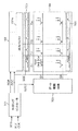
実施の形態1.
図8を参照すると、本発明の実施の形態1による液晶表示装置は、ゲートライン(G1〜Gn)とデータライン(D1〜Dm)とがそれぞれ交差し、その交差部に液晶セルClcが複数配列された液晶セルアレイが形成された液晶パネル104と、ゲートラインにスキャンパルスを供給するためのゲート駆動回路103と、データラインにデータ電圧を供給するためのデータ駆動回路102と、データライン(D1〜Dm)をプリチャージするための第1及び第2のチャージシェア回路106、105と、データ駆動回路102、ゲート駆動回路103、第1及び第2のチャージシェア回路106、105を制御するためのタイミングコントローラ101とを備える。
Referring to FIG. 8, in the liquid crystal display according to the first embodiment of the present invention, the gate lines (G1 to Gn) and the data lines (D1 to Dm) intersect with each other, and a plurality of liquid crystal cells Clc are arranged at the intersections. A
液晶パネル104は、2枚のガラス基板の間に液晶が注入されて形成され、その下部ガラス基板上には、データライン(D1〜Dm)とゲートライン(G1〜Gn)とが互いに直交して形成される。データライン(D1〜Dm)とゲートライン(G1〜Gn)とのそれぞれの交差部に形成されたTFTは、ゲートライン(G1〜Gn)からのスキャンパルスに応じて、データライン(D1〜Dm)上のデータ電圧を液晶セルClcに供給する。そこで、TFTのゲート電極は、ゲートライン(G1〜Gn)に接続され、TFTのソース電極は、データライン(D1〜Dm)に接続される。TFTのドレーン電極は、液晶セルClcの画素電極に接続される。画素電極と対向する共通電極には、共通電圧Vcomが供給される。
The
そして、液晶パネル104の各液晶セルClcには、液晶セルClcに充電された電圧を一定に維持するためのストレージキャパシターCstが形成される。液晶パネル104の下端部の液晶セルアレイの外方には、第1のチャージシェア回路106が形成される。この第1のチャージシェア回路106は、複数のスイッチング素子SW1を含む。スイッチング素子SW1は、それぞれのデータライン(D1〜Dm)に接続され、タイミングコントローラ101からのソース出力信号SOEに応じて、データライン(D1〜Dm)を同時に遮断する。
In each liquid crystal cell Clc of the
データ駆動回路102は、所定のチャンネル数を有する複数のデータ集積回路を含む。ここで、データ集積回路は、クロックをサンプリングするためのシフトレジスタ、データを一時保存するためのレジスタ、シフトレジスタからのクロック信号に応じてデータを1ライン分ずつ保存し、保存された1ライン分のデータを同時に出力するためのラッチ、ラッチからのデータ値に対応して、正極性/負極性のガンマ電圧を選択するためのデジタル−アナログ変換器、正極性/負極性のガンマ電圧により変換されたアナログデータ(ビデオ信号)が供給されるデータライン(D1〜Dm)を選択するためのマルチプレクサ、マルチプレクサと選択されたデータラインとの間に接続された出力バッファ102a、及び出力バッファ102aの出力端に形成された第2のチャージシェア回路105などで構成される。
The
この第2のチャージシェア回路105は、複数のスイッチング素子SW2を含む。スイッチング素子SW2は、それぞれのデータライン(D1〜Dm)に接続され、タイミングコントローラ101からのソース出力信号SOEに応じて、データライン(D1〜Dm)を同時に遮断する。このようなデータ集積回路は、タイミングコントローラ101の制御下で、データライン(D1〜Dm)にデータ電圧、即ちビデオ信号を供給する。
ゲート駆動回路103は、スキャンパルスを順次発生するシフトレジスタと、スキャンパルスの電圧を液晶セルClcの駆動に適したレベルにシフトさせるためのレベルシフタなどで構成される。このゲート駆動回路103は、タイミングコントローラ101の制御下で、ゲートライン(G1〜Gn)に、ビデオ信号に同期するスキャンパルスを順次供給する。
The second
The
タイミングコントローラ101は、垂直/水平同期信号V、HとクロックCLKとを用いて、ゲート駆動回路103を制御するためのゲート制御信号GDCと、データ駆動回路102を制御するためのデータ制御信号DDCとを発生する。データ制御信号DDCは、ソーススタートパルス(Source Start Pulse:SSP)、ソースシフトクロック(Source Shift Clock:SSC)、ソース出力信号(Source Output Enable:SOE)、極性信号(Polarity:POL)などを含む。ゲート制御信号GDCは、ゲートシフトクロック(Gate Shift Clock:GSC)、ゲート出力信号(Gate Output Enable:GOE)、ゲートスタートパルス(Gate Start Pulse:GSP)などを含む。
The
図9は、データライン(D1〜Dm)を介して各液晶セルClcに供給される信号を示し、「SOE」は、ソース出力信号を、「POL」は、極性信号を、「D」は、ビデオ信号をそれぞれ示す。ビデオ信号Dは、極性信号POLにより、その極性が制御され、ソース出力信号SOEがロー状態(ロー区間)である場合にデータライン(D1〜Dm)に供給される。
以下、図9を参照して、第1及び第2のチャージシェア回路106、105によるチャージシェアリング過程について説明する。
FIG. 9 shows signals supplied to the respective liquid crystal cells Clc through the data lines (D1 to Dm). “SOE” is a source output signal, “POL” is a polarity signal, and “D” is Each video signal is shown. The polarity of the video signal D is controlled by the polarity signal POL, and is supplied to the data lines (D1 to Dm) when the source output signal SOE is in the low state (low period).
Hereinafter, the charge sharing process by the first and second
まず、ソース出力信号SOEのロー区間において、出力バッファ102aから正極性または負極性のビデオ信号Dが、データライン(D1〜Dm)に供給され、液晶パネル104に、ビデオ信号Dに対応される所定の画像が表示される。
First, in the low period of the source output signal SOE, the positive or negative video signal D is supplied from the
そして、ソース出力信号SOEのハイ区間において、第1及び第2のチャージシェア回路106、105の第1及び第2のスイッチング素子SW1、SW2がターンオンされる。第1及び第2のスイッチング素子SW1、SW2がターンオンされると、全てのデータライン(D1〜Dm)が電気的に接続される。このとき、データライン(D1〜Dm)には、前回のソース出力信号SOEのロー区間において供給されたビデオ信号Dにより、各液晶セルClcに充電されたビデオ信号Dの平均電圧が示される。
In the high period of the source output signal SOE, the first and second switching elements SW1 and SW2 of the first and second
以後、ソース出力信号SOEがロー状態に反転すると、負極性または正極性のビデオ信号Dがデータライン(D1〜Dm)に供給され、液晶パネル104に所定の画像が表示される。
Thereafter, when the source output signal SOE is inverted to the low state, the negative or positive video signal D is supplied to the data lines (D1 to Dm), and a predetermined image is displayed on the
このように、データライン(D1〜Dm)をプリチャージ(Pre-Chargeing)させることで、電圧変動レベルを最小化し、消費電力の低減及びデータ集積回路の発熱が減少する效果がある。特に、液晶セルアレイの両端におけるチャージシェアリングによるデータ電圧の波形をそれぞれ示す図10a及び図10bを参照すると、第1及び第2のチャージシェア回路106、105が、液晶セルアレイの一端側及び他端側で同時にチャージシェアリングを行うことにより、従来のチャージシェア回路から遠くなるほどチャージシェアリングの效果が減少するという問題点を克服し、效果を向上させることができる。
As described above, pre-charging the data lines D1 to Dm has the effect of minimizing the voltage fluctuation level, reducing power consumption, and reducing heat generation of the data integrated circuit. In particular, referring to FIGS. 10a and 10b showing waveforms of data voltages due to charge sharing at both ends of the liquid crystal cell array, the first and second
実施の形態2.
図11は、本発明の第2の実施例による液晶表示装置を示す。
図11を参照すると、本発明の実施の形態2による液晶表示装置は、ゲートライン(G1〜Gn)とデータライン(D1〜Dm)とがそれぞれ交差し、その交差部に液晶セルClcが複数配列された液晶セルアレイが形成された液晶パネル204と、ゲートラインにスキャンパルスを供給するためのゲート駆動回路203と、データラインにデータ電圧を供給するためのデータ駆動回路202と、データライン(D1〜Dm)をプリチャージするための第1及び第2のチャージシェア回路206、205と、データ駆動回路202、ゲート駆動回路203、第1及び第2のチャージシェア回路206、205を制御するためのタイミングコントローラ201とを備える。
Embodiment 2. FIG.
FIG. 11 shows a liquid crystal display device according to a second embodiment of the present invention.
Referring to FIG. 11, in the liquid crystal display according to the second embodiment of the present invention, the gate lines (G1 to Gn) and the data lines (D1 to Dm) intersect with each other, and a plurality of liquid crystal cells Clc are arranged at the intersections. A
液晶パネル204は、2枚のガラス基板の間に液晶が注入されて形成され、その下部ガラス基板上には、データライン(D1〜Dm)とゲートライン(G1〜Gn)とが互いに直交して形成される。データライン(D1〜Dm)とゲートライン(G1〜Gn)とのそれぞれの交差部に形成されたTFTは、ゲートライン(G1〜Gn)からのスキャンパルスに応じて、データライン(D1〜Dm)上のデータ電圧を液晶セルClcに供給する。そこで、TFTのゲート電極は、ゲートライン(G1〜Gn)に接続され、TFTのソース電極は、データライン(D1〜Dm)に接続される。TFTのドレーン電極は、液晶セルClcの画素電極に接続される。画素電極と対向する共通電極には、共通電圧Vcomが供給される。
The
そして、液晶パネル204の各液晶セルClcには、液晶セルClcに充電された電圧を一定に維持するためのストレージキャパシターCstが形成される。液晶パネル204の液晶セルアレイの一端側及び他端側の外方には、第1及び第2のチャージシェア回路206、205が形成される。この1及び第2のチャージシェア回路206、205は、それぞれ複数のスイッチング素子SW1、SW2を含む。スイッチング素子SW1、SW2は、それぞれのデータライン(D1〜Dm)に接続され、タイミングコントローラ201からのソース出力信号SOEに応じて、データライン(D1〜Dm)を同時に遮断する。
In each liquid crystal cell Clc of the
データ駆動回路202は、所定のチャンネル数を有する複数のデータ集積回路を含む。ここで、データ集積回路は、クロックをサンプリングするためのシフトレジスタ、データを一時保存するためのレジスタ、シフトレジスタからのクロック信号に応じて、データを1ライン分ずつ保存し、保存された1ライン分のデータを同時に出力するためのラッチ、ラッチからのデータ値に対応して、正極性/負極性のガンマ電圧を選択するためのデジタル−アナログ変換器、正極性/負極性のガンマ電圧によって変換されたアナログデータ(ビデオ信号)が供給されるデータライン(D1〜Dm)を選択するためのマルチプレクサ、及びマルチプレクサと選択されたデータラインとの間に接続された出力バッファなどで構成される。このようなデータ集積回路は、タイミングコントローラ201の制御下で、データライン(D1〜Dm)にデータ電圧、即ちビデオ信号Dを供給する。
The
ゲート駆動回路203は、スキャンパルスを順次発生するシフトレジスタと、スキャンパルスの電圧を液晶セルClcの駆動に適したレベルにシフトさせるためのレベルシフタなどで構成される。このゲート駆動回路203は、タイミングコントローラ201の制御下で、ゲートライン(G1〜Gn)に、ビデオ信号Dに同期するスキャンパルスを順次供給する。
The
タイミングコントローラ201は、垂直/水平同期信号V、HとクロックCLKとを用いて、ゲート駆動回路203を制御するためのゲート制御信号GDCと、データ駆動回路202とを制御するためのデータ制御信号DDCを発生する。データ制御信号DDCは、ソーススタートパルス(Source Start Pulse:SSP)、ソースシフトクロック(Source Shift Clock:SSC)、ソース出力信号(Source Output Enable:SOE)、極性信号(Polarity:POL)などを含む。ゲート制御信号GDCは、ゲートシフトクロック(Gate Shift Clock:GSC)、ゲート出力信号(Gate Output Enable:GOE)、ゲートスタートパルス(Gate Start Pulse:GSP)などを含む。
第1及び第2のチャージシェア回路206、205によるチャージシェアリング過程に関する説明は、上記実施の形態1と同様であるため、省略する。
The
The description of the charge sharing process by the first and second
以上説明した内容に基づいて、当業者であれば、本発明の技術的思想を逸脱しない範囲内で種々の変更及び修正が可能であることがわかるだろう。従って、本発明の技術的範囲は、明細書の詳細な説明に記載した内容に限定されるのではなく、特許請求の範囲により定めなければならない。 Based on the above description, those skilled in the art will recognize that various changes and modifications can be made without departing from the technical idea of the present invention. Therefore, the technical scope of the present invention is not limited to the contents described in the detailed description of the specification, but must be defined by the claims.
11、101、201 タイミングコントローラ、12、102、202 データ駆動回路、13、103、203 ゲート駆動回路、14、104、204 液晶パネル、102a 出力バッファ、105、205 第2チャージシェア回路、106、206 第1チャージシェア回路、Clc 液晶セル、D ビデオ信号、SOE ソース出力信号、SW1、SW2 スイッチング素子。
11, 101, 201 Timing controller, 12, 102, 202 Data drive circuit, 13, 103, 203 Gate drive circuit, 14, 104, 204 Liquid crystal panel, 102a Output buffer, 105, 205 Second charge share circuit, 106, 206 First charge share circuit, Clc liquid crystal cell, D video signal, SOE source output signal, SW1, SW2 switching element.
Claims (11)
前記液晶セルアレイの一端側の外方に配置され、前記データラインにデータ電圧が充電される前に、前記データラインをプリチャージするための第1のチャージシェア回路と、
前記液晶セルアレイの他端側の外方に配置され、前記データラインにデータ電圧が充電される前に、前記データラインをプリチャージするための第2のチャージシェア回路と
を備えることを特徴とする液晶表示装置。 A liquid crystal cell array in which a plurality of gate lines and a plurality of data lines cross each other and a plurality of liquid crystal cells are arranged,
A first charge sharing circuit disposed outside one end of the liquid crystal cell array, for precharging the data line before the data line is charged with a data voltage;
A second charge share circuit disposed outside the other end of the liquid crystal cell array and for precharging the data line before the data line is charged with a data voltage. Liquid crystal display device.
前記データラインに前記データ電圧を供給するためのデータ駆動回路と、
前記ゲートラインにスキャンパルスを供給するためのゲート駆動回路と、
前記データ駆動回路、前記ゲート駆動回路、前記第1及び第2のチャージシェア回路を制御するためのタイミングコントローラと
をさらに備えることを特徴とする請求項2に記載の液晶表示装置。 A liquid crystal panel on which the liquid crystal cell array is formed;
A data driving circuit for supplying the data voltage to the data line;
A gate driving circuit for supplying a scan pulse to the gate line;
The liquid crystal display device according to claim 2, further comprising: a timing controller for controlling the data driving circuit, the gate driving circuit, and the first and second charge sharing circuits.
前記液晶セルアレイの他端側の外方に配置され、前記データラインにデータ電圧が充電される前に、前記データラインをプリチャージするための第2のチャージシェア回路と
を備えることを特徴とするチャージシェア装置。 A plurality of liquid crystal cells are arranged outside one end side of the liquid crystal cell array and connected to the liquid crystal cells before the data voltage is charged to the data lines supplying the video signals. A first charge share circuit for precharging;
A second charge share circuit disposed outside the other end of the liquid crystal cell array and for precharging the data line before the data line is charged with a data voltage. Charge sharing device.
The method of claim 9, wherein the first and second charge share circuits include a switching element connected to the data line, and the switching element is operated simultaneously according to a source output signal. Charge sharing device.
Applications Claiming Priority (1)
| Application Number | Priority Date | Filing Date | Title |
|---|---|---|---|
| KR1020050077302A KR20070023099A (en) | 2005-08-23 | 2005-08-23 | LCD and its driving method |
Publications (1)
| Publication Number | Publication Date |
|---|---|
| JP2007058177A true JP2007058177A (en) | 2007-03-08 |
Family
ID=36745725
Family Applications (1)
| Application Number | Title | Priority Date | Filing Date |
|---|---|---|---|
| JP2006176752A Pending JP2007058177A (en) | 2005-08-23 | 2006-06-27 | Liquid crystal display device, driving method of liquid crystal display device, and charge share circuit |
Country Status (8)
| Country | Link |
|---|---|
| US (1) | US7817126B2 (en) |
| JP (1) | JP2007058177A (en) |
| KR (1) | KR20070023099A (en) |
| CN (1) | CN100426063C (en) |
| DE (1) | DE102006027401B4 (en) |
| FR (1) | FR2890224B1 (en) |
| GB (1) | GB2429569B (en) |
| TW (1) | TWI373745B (en) |
Cited By (4)
| Publication number | Priority date | Publication date | Assignee | Title |
|---|---|---|---|---|
| JP2013231939A (en) * | 2012-04-30 | 2013-11-14 | Lg Display Co Ltd | Liquid crystal display device and method for driving the same |
| US8803855B2 (en) | 2010-04-22 | 2014-08-12 | Samsung Display Co., Ltd. | Liquid crystal display, method of driving the same, and method of manufacturing the same |
| US9099055B2 (en) | 2011-11-10 | 2015-08-04 | Samsung Electronics Co., Ltd. | Display driving device and display system with improved protection against electrostatic discharge |
| US9158165B2 (en) | 2010-03-08 | 2015-10-13 | Samsung Display Co., Ltd. | Display device having plurality of charge share gate lines |
Families Citing this family (36)
| Publication number | Priority date | Publication date | Assignee | Title |
|---|---|---|---|---|
| CN101233556B (en) | 2005-08-01 | 2012-01-25 | 夏普株式会社 | Display device, its drive circuit, and drive method |
| WO2007015348A1 (en) | 2005-08-04 | 2007-02-08 | Sharp Kabushiki Kaisha | Display device and its drive method |
| JP4812837B2 (en) * | 2006-07-14 | 2011-11-09 | シャープ株式会社 | Active matrix substrate and display device including the same |
| WO2008015813A1 (en) | 2006-08-02 | 2008-02-07 | Sharp Kabushiki Kaisha | Active matrix substrate and display device with same |
| CN101467200B (en) | 2006-09-28 | 2011-09-28 | 夏普株式会社 | Liquid crystal display device, driving circuit and driving method thereof |
| EP2053589A4 (en) | 2006-11-02 | 2011-01-12 | Sharp Kk | Active matrix substrate, and display device having the substrate |
| KR100849214B1 (en) * | 2007-01-16 | 2008-07-31 | 삼성전자주식회사 | Data Driver Device and Display Device capable of reducing charge share power consumption |
| KR101287477B1 (en) * | 2007-05-01 | 2013-07-19 | 엘지디스플레이 주식회사 | Liquid crystal display device |
| KR101405341B1 (en) * | 2007-10-30 | 2014-06-12 | 삼성디스플레이 주식회사 | Liquid crystal display device with improved visibility |
| KR101102358B1 (en) * | 2009-11-30 | 2012-01-05 | 주식회사 실리콘웍스 | Display panel drive circuit and driving method thereof |
| KR101660977B1 (en) * | 2009-12-21 | 2016-09-28 | 엘지디스플레이 주식회사 | Liquid crystal display |
| KR101676608B1 (en) * | 2009-12-29 | 2016-11-16 | 엘지디스플레이 주식회사 | Liquid Crystal Display Device and Driving Method the same |
| TWI517128B (en) * | 2010-04-08 | 2016-01-11 | 友達光電股份有限公司 | Display device, display device driving method and source driving circuit |
| CN102346341B (en) * | 2010-08-04 | 2014-09-10 | 北京京东方光电科技有限公司 | Array base plate, manufacturing method for array base plate, liquid crystal panel, liquid crystal display and driving method |
| TWI430707B (en) * | 2010-11-18 | 2014-03-11 | Au Optronics Corp | Liquid crystal display and source driving apparatus and driving method of panel thereof |
| US8896586B2 (en) | 2010-12-15 | 2014-11-25 | Novatek Microelectronics Corp. | Gate driving method for controlling display apparatus and gate driver using the same |
| CN102157136B (en) * | 2011-02-24 | 2012-12-12 | 深圳市华星光电技术有限公司 | Liquid crystal display and driving method thereof |
| CN102779492B (en) * | 2011-10-08 | 2014-10-29 | 北京京东方光电科技有限公司 | Liquid crystal display drive method and drive device |
| TWI456558B (en) * | 2012-05-10 | 2014-10-11 | Himax Tech Ltd | Image display |
| CN103456260B (en) * | 2012-05-28 | 2016-03-30 | 奇景光电股份有限公司 | Image display |
| CN103514842B (en) * | 2012-06-26 | 2015-08-05 | 奇景光电股份有限公司 | Image display |
| CN102929019B (en) * | 2012-10-19 | 2016-01-20 | 京东方科技集团股份有限公司 | A kind of gate drive apparatus, display panel and display device |
| CN103543567B (en) * | 2013-11-11 | 2016-03-30 | 北京京东方光电科技有限公司 | A kind of array base palte and driving method, display device |
| KR102135635B1 (en) * | 2013-11-20 | 2020-07-20 | 엘지디스플레이 주식회사 | Data driving integrated circuit and liquid crystal display device including the same |
| KR20160074856A (en) * | 2014-12-18 | 2016-06-29 | 삼성디스플레이 주식회사 | Display device |
| CN108020967B (en) * | 2016-11-01 | 2021-01-26 | 京东方科技集团股份有限公司 | Array substrate, liquid crystal display panel and display device |
| CN107293266A (en) * | 2017-07-19 | 2017-10-24 | 深圳市华星光电半导体显示技术有限公司 | A kind of liquid crystal display panel and device |
| CN107831614A (en) * | 2017-11-07 | 2018-03-23 | 深圳市华星光电半导体显示技术有限公司 | Pixel driving framework and display device |
| CN108172162A (en) * | 2018-01-02 | 2018-06-15 | 京东方科技集团股份有限公司 | A kind of array substrate driving method, driving device and display device |
| KR102549888B1 (en) * | 2018-02-08 | 2023-07-03 | 삼성디스플레이 주식회사 | Method of operating a display device supporting a normal mode and a variable frame mode, and the display device |
| CN108615509B (en) * | 2018-05-07 | 2022-07-19 | 京东方科技集团股份有限公司 | Display device and driving method thereof |
| US11056068B2 (en) * | 2018-11-30 | 2021-07-06 | Sharp Kabushiki Kaisha | Display device performing precharge of video signal lines and drive method thereof |
| CN110459182A (en) * | 2019-06-11 | 2019-11-15 | 惠科股份有限公司 | Charge sharing circuit and method of display panel and display panel |
| US10950186B2 (en) * | 2019-07-26 | 2021-03-16 | Novatek Microelectronics Corp. | Display apparatus and method thereof |
| CN113867061A (en) * | 2021-09-30 | 2021-12-31 | 上海天马微电子有限公司 | Array substrate, driving method of array substrate and display device |
| CN114399979B (en) * | 2021-12-20 | 2023-03-24 | 北京奕斯伟计算技术股份有限公司 | A circuit structure and display driver chip |
Citations (7)
| Publication number | Priority date | Publication date | Assignee | Title |
|---|---|---|---|---|
| JPH10115839A (en) * | 1996-10-11 | 1998-05-06 | Sanyo Electric Co Ltd | Liquid crystal display device |
| JPH10326090A (en) * | 1997-05-23 | 1998-12-08 | Sony Corp | Active matrix display device |
| JP2001235723A (en) * | 2000-02-24 | 2001-08-31 | Matsushita Electric Ind Co Ltd | Liquid crystal display |
| JP2002268613A (en) * | 2001-02-26 | 2002-09-20 | Samsung Electronics Co Ltd | Liquid crystal display device and driving method thereof |
| JP2005025179A (en) * | 2003-06-10 | 2005-01-27 | Oki Electric Ind Co Ltd | Driving circuit |
| JP2005091505A (en) * | 2003-09-12 | 2005-04-07 | Sony Corp | Display device |
| JP2005201974A (en) * | 2004-01-13 | 2005-07-28 | Oki Electric Ind Co Ltd | Output circuit, and circuit and method for driving liquid crystal |
Family Cites Families (15)
| Publication number | Priority date | Publication date | Assignee | Title |
|---|---|---|---|---|
| US5555001A (en) * | 1994-03-08 | 1996-09-10 | Prime View Hk Limited | Redundant scheme for LCD display with integrated data driving circuit |
| US5528256A (en) * | 1994-08-16 | 1996-06-18 | Vivid Semiconductor, Inc. | Power-saving circuit and method for driving liquid crystal display |
| JP2001305509A (en) * | 2000-04-10 | 2001-10-31 | Ind Technol Res Inst | Drive circuit for multi-stage liquid crystal display charging |
| JP4894081B2 (en) | 2000-06-14 | 2012-03-07 | ソニー株式会社 | Display device and driving method thereof |
| CN1372214A (en) * | 2001-02-19 | 2002-10-02 | 意蓝科技股份有限公司 | User Behavior Oriented Network Marketing System and Its Processing Method |
| JP3623175B2 (en) * | 2001-05-08 | 2005-02-23 | 松下電器産業株式会社 | Signal transmission circuit |
| JP2002351427A (en) * | 2001-05-29 | 2002-12-06 | Matsushita Electric Ind Co Ltd | Image display device and image display method |
| TWI286732B (en) * | 2001-12-19 | 2007-09-11 | Himax Tech Ltd | Method for driving an LCD with a class-A operational amplifier |
| KR20030064466A (en) | 2002-01-28 | 2003-08-02 | 일진다이아몬드(주) | Active matrix display device |
| US7079092B2 (en) * | 2003-04-25 | 2006-07-18 | Barco Nv | Organic light-emitting diode (OLED) pre-charge circuit for use in a common anode large-screen display |
| KR100965571B1 (en) * | 2003-06-30 | 2010-06-23 | 엘지디스플레이 주식회사 | LCD and its driving method |
| JP4425620B2 (en) * | 2003-12-12 | 2010-03-03 | Necエレクトロニクス株式会社 | Output circuit |
| TWI247220B (en) * | 2004-01-16 | 2006-01-11 | Via Tech Inc | 3D image processing method |
| GB0403308D0 (en) * | 2004-02-14 | 2004-03-17 | Koninkl Philips Electronics Nv | Active matrix display devices |
| US7649787B2 (en) * | 2006-09-05 | 2010-01-19 | Semiconductor Energy Laboratory Co., Ltd. | Semiconductor device |
-
2005
- 2005-08-23 KR KR1020050077302A patent/KR20070023099A/en not_active Ceased
-
2006
- 2006-06-12 GB GB0611586A patent/GB2429569B/en not_active Expired - Fee Related
- 2006-06-13 DE DE102006027401A patent/DE102006027401B4/en not_active Expired - Fee Related
- 2006-06-14 TW TW095121303A patent/TWI373745B/en not_active IP Right Cessation
- 2006-06-15 FR FR0605337A patent/FR2890224B1/en not_active Expired - Fee Related
- 2006-06-15 CN CNB2006100871794A patent/CN100426063C/en not_active Expired - Fee Related
- 2006-06-27 JP JP2006176752A patent/JP2007058177A/en active Pending
- 2006-06-27 US US11/476,368 patent/US7817126B2/en active Active
Patent Citations (7)
| Publication number | Priority date | Publication date | Assignee | Title |
|---|---|---|---|---|
| JPH10115839A (en) * | 1996-10-11 | 1998-05-06 | Sanyo Electric Co Ltd | Liquid crystal display device |
| JPH10326090A (en) * | 1997-05-23 | 1998-12-08 | Sony Corp | Active matrix display device |
| JP2001235723A (en) * | 2000-02-24 | 2001-08-31 | Matsushita Electric Ind Co Ltd | Liquid crystal display |
| JP2002268613A (en) * | 2001-02-26 | 2002-09-20 | Samsung Electronics Co Ltd | Liquid crystal display device and driving method thereof |
| JP2005025179A (en) * | 2003-06-10 | 2005-01-27 | Oki Electric Ind Co Ltd | Driving circuit |
| JP2005091505A (en) * | 2003-09-12 | 2005-04-07 | Sony Corp | Display device |
| JP2005201974A (en) * | 2004-01-13 | 2005-07-28 | Oki Electric Ind Co Ltd | Output circuit, and circuit and method for driving liquid crystal |
Cited By (5)
| Publication number | Priority date | Publication date | Assignee | Title |
|---|---|---|---|---|
| US9158165B2 (en) | 2010-03-08 | 2015-10-13 | Samsung Display Co., Ltd. | Display device having plurality of charge share gate lines |
| US8803855B2 (en) | 2010-04-22 | 2014-08-12 | Samsung Display Co., Ltd. | Liquid crystal display, method of driving the same, and method of manufacturing the same |
| US9099055B2 (en) | 2011-11-10 | 2015-08-04 | Samsung Electronics Co., Ltd. | Display driving device and display system with improved protection against electrostatic discharge |
| JP2013231939A (en) * | 2012-04-30 | 2013-11-14 | Lg Display Co Ltd | Liquid crystal display device and method for driving the same |
| US9483131B2 (en) | 2012-04-30 | 2016-11-01 | Lg Display Co., Ltd. | Liquid crystal display and method of driving the same |
Also Published As
| Publication number | Publication date |
|---|---|
| US20070046613A1 (en) | 2007-03-01 |
| DE102006027401A1 (en) | 2007-03-15 |
| KR20070023099A (en) | 2007-02-28 |
| FR2890224A1 (en) | 2007-03-02 |
| CN100426063C (en) | 2008-10-15 |
| GB2429569B (en) | 2007-11-07 |
| GB2429569A (en) | 2007-02-28 |
| CN1920624A (en) | 2007-02-28 |
| TW200709143A (en) | 2007-03-01 |
| TWI373745B (en) | 2012-10-01 |
| GB0611586D0 (en) | 2006-07-19 |
| FR2890224B1 (en) | 2010-01-15 |
| DE102006027401B4 (en) | 2009-05-14 |
| US7817126B2 (en) | 2010-10-19 |
Similar Documents
| Publication | Publication Date | Title |
|---|---|---|
| JP2007058177A (en) | Liquid crystal display device, driving method of liquid crystal display device, and charge share circuit | |
| US7403185B2 (en) | Liquid crystal display device and method of driving the same | |
| KR101450868B1 (en) | Display device and driving method thereof | |
| US7420533B2 (en) | Liquid crystal display and driving method thereof | |
| JP4786996B2 (en) | Display device | |
| US8269706B2 (en) | Operating unit of liquid crystal display panel and method for operating the same | |
| US20080150865A1 (en) | Lcd and drive method thereof | |
| JP4566975B2 (en) | Liquid crystal display device and driving method thereof | |
| KR100480180B1 (en) | Liquid crystal display apparatus driven 2-dot inversion type and method of dirving the same | |
| KR20080086060A (en) | LCD and its driving method | |
| KR20090004234A (en) | LCD and its driving method | |
| KR101192759B1 (en) | Apparatus and method for driving liquid crystal display device | |
| KR20070080427A (en) | LCD and its driving method | |
| KR101174783B1 (en) | Apparatus and method for driving of liquid crystal display device | |
| KR100880934B1 (en) | LCD and Driving Method | |
| KR20100009212A (en) | Driving method of liquid crystal display device | |
| KR100680057B1 (en) | Precharging method and apparatus of liquid crystal display | |
| KR20070069797A (en) | LCD and its driving method | |
| KR20080026278A (en) | Data driving device and driving method thereof | |
| KR20130010576A (en) | Liquid crystal display device and method of driving the same | |
| KR101415686B1 (en) | Source driving circuit and driving method thereof | |
| KR100928929B1 (en) | Inversion driving device and method of liquid crystal display device | |
| KR101467213B1 (en) | A driving device of a 2 dot inversion liquid crystal display device | |
| KR20080097530A (en) | LCD and its driving method | |
| KR100920375B1 (en) | LCD and its driving method |
Legal Events
| Date | Code | Title | Description |
|---|---|---|---|
| A977 | Report on retrieval |
Free format text: JAPANESE INTERMEDIATE CODE: A971007 Effective date: 20090409 |
|
| A131 | Notification of reasons for refusal |
Free format text: JAPANESE INTERMEDIATE CODE: A131 Effective date: 20090421 |
|
| A521 | Request for written amendment filed |
Free format text: JAPANESE INTERMEDIATE CODE: A523 Effective date: 20090721 |
|
| A02 | Decision of refusal |
Free format text: JAPANESE INTERMEDIATE CODE: A02 Effective date: 20090825 |
|
| A521 | Request for written amendment filed |
Free format text: JAPANESE INTERMEDIATE CODE: A523 Effective date: 20091225 |
|
| A911 | Transfer to examiner for re-examination before appeal (zenchi) |
Free format text: JAPANESE INTERMEDIATE CODE: A911 Effective date: 20100224 |
|
| A912 | Re-examination (zenchi) completed and case transferred to appeal board |
Free format text: JAPANESE INTERMEDIATE CODE: A912 Effective date: 20100402 |
|
| A601 | Written request for extension of time |
Free format text: JAPANESE INTERMEDIATE CODE: A601 Effective date: 20110209 |
|
| A602 | Written permission of extension of time |
Free format text: JAPANESE INTERMEDIATE CODE: A602 Effective date: 20110217 |
|
| A601 | Written request for extension of time |
Free format text: JAPANESE INTERMEDIATE CODE: A601 Effective date: 20110309 |
|
| A602 | Written permission of extension of time |
Free format text: JAPANESE INTERMEDIATE CODE: A602 Effective date: 20110316 |
|
| A601 | Written request for extension of time |
Free format text: JAPANESE INTERMEDIATE CODE: A601 Effective date: 20110411 |
|
| A602 | Written permission of extension of time |
Free format text: JAPANESE INTERMEDIATE CODE: A602 Effective date: 20110414 |