JP2005340602A - Semiconductor device and its fabrication process - Google Patents
Semiconductor device and its fabrication process Download PDFInfo
- Publication number
- JP2005340602A JP2005340602A JP2004159070A JP2004159070A JP2005340602A JP 2005340602 A JP2005340602 A JP 2005340602A JP 2004159070 A JP2004159070 A JP 2004159070A JP 2004159070 A JP2004159070 A JP 2004159070A JP 2005340602 A JP2005340602 A JP 2005340602A
- Authority
- JP
- Japan
- Prior art keywords
- film
- barrier metal
- metal film
- wiring
- conductive
- Prior art date
- Legal status (The legal status is an assumption and is not a legal conclusion. Google has not performed a legal analysis and makes no representation as to the accuracy of the status listed.)
- Pending
Links
- 238000000034 method Methods 0.000 title claims abstract description 94
- 239000004065 semiconductor Substances 0.000 title claims abstract description 40
- 238000004519 manufacturing process Methods 0.000 title claims description 12
- 229910052751 metal Inorganic materials 0.000 claims abstract description 62
- 239000002184 metal Substances 0.000 claims abstract description 62
- 230000004888 barrier function Effects 0.000 claims abstract description 60
- 239000004020 conductor Substances 0.000 claims abstract description 16
- 239000010949 copper Substances 0.000 claims description 92
- 239000000758 substrate Substances 0.000 claims description 39
- 238000005530 etching Methods 0.000 claims description 36
- 238000005498 polishing Methods 0.000 claims description 24
- 239000007788 liquid Substances 0.000 claims description 21
- 239000000463 material Substances 0.000 claims description 21
- 150000007524 organic acids Chemical class 0.000 claims description 9
- 238000000151 deposition Methods 0.000 claims description 7
- 239000007800 oxidant agent Substances 0.000 claims description 6
- 229910052802 copper Inorganic materials 0.000 claims description 3
- 230000008021 deposition Effects 0.000 claims description 3
- RYGMFSIKBFXOCR-UHFFFAOYSA-N Copper Chemical compound [Cu] RYGMFSIKBFXOCR-UHFFFAOYSA-N 0.000 claims description 2
- 230000015556 catabolic process Effects 0.000 abstract description 21
- 239000010408 film Substances 0.000 description 301
- 229910004298 SiO 2 Inorganic materials 0.000 description 34
- 238000005229 chemical vapour deposition Methods 0.000 description 22
- 239000010410 layer Substances 0.000 description 19
- 230000015572 biosynthetic process Effects 0.000 description 17
- 239000000243 solution Substances 0.000 description 16
- 238000010586 diagram Methods 0.000 description 14
- 235000012431 wafers Nutrition 0.000 description 14
- 238000004140 cleaning Methods 0.000 description 12
- 239000007789 gas Substances 0.000 description 11
- 239000002002 slurry Substances 0.000 description 11
- QGZKDVFQNNGYKY-UHFFFAOYSA-N Ammonia Chemical compound N QGZKDVFQNNGYKY-UHFFFAOYSA-N 0.000 description 8
- 239000011229 interlayer Substances 0.000 description 8
- XLYOFNOQVPJJNP-UHFFFAOYSA-N water Substances O XLYOFNOQVPJJNP-UHFFFAOYSA-N 0.000 description 8
- 238000009832 plasma treatment Methods 0.000 description 7
- KRKNYBCHXYNGOX-UHFFFAOYSA-N citric acid Chemical compound OC(=O)CC(O)(C(O)=O)CC(O)=O KRKNYBCHXYNGOX-UHFFFAOYSA-N 0.000 description 6
- 230000000694 effects Effects 0.000 description 6
- 238000005240 physical vapour deposition Methods 0.000 description 6
- 238000012545 processing Methods 0.000 description 6
- 238000004544 sputter deposition Methods 0.000 description 6
- MZLGASXMSKOWSE-UHFFFAOYSA-N tantalum nitride Chemical compound [Ta]#N MZLGASXMSKOWSE-UHFFFAOYSA-N 0.000 description 6
- 238000000231 atomic layer deposition Methods 0.000 description 5
- 238000009792 diffusion process Methods 0.000 description 5
- 238000007517 polishing process Methods 0.000 description 5
- 239000000126 substance Substances 0.000 description 5
- MHAJPDPJQMAIIY-UHFFFAOYSA-N Hydrogen peroxide Chemical compound OO MHAJPDPJQMAIIY-UHFFFAOYSA-N 0.000 description 4
- 229910045601 alloy Inorganic materials 0.000 description 4
- 239000000956 alloy Substances 0.000 description 4
- 229910021529 ammonia Inorganic materials 0.000 description 4
- 239000012528 membrane Substances 0.000 description 4
- 239000011148 porous material Substances 0.000 description 4
- 229910052710 silicon Inorganic materials 0.000 description 4
- QTBSBXVTEAMEQO-UHFFFAOYSA-N Acetic acid Chemical compound CC(O)=O QTBSBXVTEAMEQO-UHFFFAOYSA-N 0.000 description 3
- OFOBLEOULBTSOW-UHFFFAOYSA-N Malonic acid Chemical compound OC(=O)CC(O)=O OFOBLEOULBTSOW-UHFFFAOYSA-N 0.000 description 3
- MUBZPKHOEPUJKR-UHFFFAOYSA-N Oxalic acid Chemical compound OC(=O)C(O)=O MUBZPKHOEPUJKR-UHFFFAOYSA-N 0.000 description 3
- XUIMIQQOPSSXEZ-UHFFFAOYSA-N Silicon Chemical compound [Si] XUIMIQQOPSSXEZ-UHFFFAOYSA-N 0.000 description 3
- 238000000277 atomic layer chemical vapour deposition Methods 0.000 description 3
- QRUDEWIWKLJBPS-UHFFFAOYSA-N benzotriazole Chemical compound C1=CC=C2N[N][N]C2=C1 QRUDEWIWKLJBPS-UHFFFAOYSA-N 0.000 description 3
- 239000012964 benzotriazole Substances 0.000 description 3
- 230000007423 decrease Effects 0.000 description 3
- 238000009713 electroplating Methods 0.000 description 3
- RAXXELZNTBOGNW-UHFFFAOYSA-N imidazole Natural products C1=CNC=N1 RAXXELZNTBOGNW-UHFFFAOYSA-N 0.000 description 3
- 239000011810 insulating material Substances 0.000 description 3
- 238000007747 plating Methods 0.000 description 3
- 239000010703 silicon Substances 0.000 description 3
- 239000004094 surface-active agent Substances 0.000 description 3
- 239000010409 thin film Substances 0.000 description 3
- XKRFYHLGVUSROY-UHFFFAOYSA-N Argon Chemical compound [Ar] XKRFYHLGVUSROY-UHFFFAOYSA-N 0.000 description 2
- FERIUCNNQQJTOY-UHFFFAOYSA-N Butyric acid Chemical compound CCCC(O)=O FERIUCNNQQJTOY-UHFFFAOYSA-N 0.000 description 2
- VZCYOOQTPOCHFL-OWOJBTEDSA-N Fumaric acid Chemical compound OC(=O)\C=C\C(O)=O VZCYOOQTPOCHFL-OWOJBTEDSA-N 0.000 description 2
- GQPLMRYTRLFLPF-UHFFFAOYSA-N Nitrous Oxide Chemical compound [O-][N+]#N GQPLMRYTRLFLPF-UHFFFAOYSA-N 0.000 description 2
- VYPSYNLAJGMNEJ-UHFFFAOYSA-N Silicium dioxide Chemical compound O=[Si]=O VYPSYNLAJGMNEJ-UHFFFAOYSA-N 0.000 description 2
- NRTOMJZYCJJWKI-UHFFFAOYSA-N Titanium nitride Chemical compound [Ti]#N NRTOMJZYCJJWKI-UHFFFAOYSA-N 0.000 description 2
- 239000002253 acid Substances 0.000 description 2
- WNLRTRBMVRJNCN-UHFFFAOYSA-N adipic acid Chemical compound OC(=O)CCCCC(O)=O WNLRTRBMVRJNCN-UHFFFAOYSA-N 0.000 description 2
- 239000007864 aqueous solution Substances 0.000 description 2
- WPYMKLBDIGXBTP-UHFFFAOYSA-N benzoic acid Chemical compound OC(=O)C1=CC=CC=C1 WPYMKLBDIGXBTP-UHFFFAOYSA-N 0.000 description 2
- 238000006243 chemical reaction Methods 0.000 description 2
- 235000015165 citric acid Nutrition 0.000 description 2
- 238000000576 coating method Methods 0.000 description 2
- 238000006731 degradation reaction Methods 0.000 description 2
- XBDQKXXYIPTUBI-UHFFFAOYSA-N dimethylselenoniopropionate Natural products CCC(O)=O XBDQKXXYIPTUBI-UHFFFAOYSA-N 0.000 description 2
- 238000001312 dry etching Methods 0.000 description 2
- 230000005684 electric field Effects 0.000 description 2
- 239000001257 hydrogen Substances 0.000 description 2
- 229910052739 hydrogen Inorganic materials 0.000 description 2
- 150000002431 hydrogen Chemical class 0.000 description 2
- 125000002887 hydroxy group Chemical group [H]O* 0.000 description 2
- 238000009413 insulation Methods 0.000 description 2
- JVTAAEKCZFNVCJ-UHFFFAOYSA-N lactic acid Chemical compound CC(O)C(O)=O JVTAAEKCZFNVCJ-UHFFFAOYSA-N 0.000 description 2
- 238000001459 lithography Methods 0.000 description 2
- 239000007769 metal material Substances 0.000 description 2
- BDAGIHXWWSANSR-UHFFFAOYSA-N methanoic acid Natural products OC=O BDAGIHXWWSANSR-UHFFFAOYSA-N 0.000 description 2
- 239000000203 mixture Substances 0.000 description 2
- 125000000896 monocarboxylic acid group Chemical group 0.000 description 2
- 239000012299 nitrogen atmosphere Substances 0.000 description 2
- 229910052760 oxygen Inorganic materials 0.000 description 2
- 238000000206 photolithography Methods 0.000 description 2
- XNGIFLGASWRNHJ-UHFFFAOYSA-N phthalic acid Chemical compound OC(=O)C1=CC=CC=C1C(O)=O XNGIFLGASWRNHJ-UHFFFAOYSA-N 0.000 description 2
- WLJVNTCWHIRURA-UHFFFAOYSA-N pimelic acid Chemical compound OC(=O)CCCCCC(O)=O WLJVNTCWHIRURA-UHFFFAOYSA-N 0.000 description 2
- 229920003209 poly(hydridosilsesquioxane) Polymers 0.000 description 2
- YGSDEFSMJLZEOE-UHFFFAOYSA-N salicylic acid Chemical compound OC(=O)C1=CC=CC=C1O YGSDEFSMJLZEOE-UHFFFAOYSA-N 0.000 description 2
- 238000007789 sealing Methods 0.000 description 2
- 229910052715 tantalum Inorganic materials 0.000 description 2
- GUVRBAGPIYLISA-UHFFFAOYSA-N tantalum atom Chemical compound [Ta] GUVRBAGPIYLISA-UHFFFAOYSA-N 0.000 description 2
- 239000010936 titanium Substances 0.000 description 2
- VZCYOOQTPOCHFL-UHFFFAOYSA-N trans-butenedioic acid Natural products OC(=O)C=CC(O)=O VZCYOOQTPOCHFL-UHFFFAOYSA-N 0.000 description 2
- 229910052721 tungsten Inorganic materials 0.000 description 2
- 239000010937 tungsten Substances 0.000 description 2
- BJEPYKJPYRNKOW-REOHCLBHSA-N (S)-malic acid Chemical compound OC(=O)[C@@H](O)CC(O)=O BJEPYKJPYRNKOW-REOHCLBHSA-N 0.000 description 1
- ITWBWJFEJCHKSN-UHFFFAOYSA-N 1,4,7-triazonane Chemical compound C1CNCCNCCN1 ITWBWJFEJCHKSN-UHFFFAOYSA-N 0.000 description 1
- RTBFRGCFXZNCOE-UHFFFAOYSA-N 1-methylsulfonylpiperidin-4-one Chemical compound CS(=O)(=O)N1CCC(=O)CC1 RTBFRGCFXZNCOE-UHFFFAOYSA-N 0.000 description 1
- OSWFIVFLDKOXQC-UHFFFAOYSA-N 4-(3-methoxyphenyl)aniline Chemical compound COC1=CC=CC(C=2C=CC(N)=CC=2)=C1 OSWFIVFLDKOXQC-UHFFFAOYSA-N 0.000 description 1
- 229910000838 Al alloy Inorganic materials 0.000 description 1
- QGZKDVFQNNGYKY-UHFFFAOYSA-O Ammonium Chemical compound [NH4+] QGZKDVFQNNGYKY-UHFFFAOYSA-O 0.000 description 1
- IJGRMHOSHXDMSA-UHFFFAOYSA-N Atomic nitrogen Chemical compound N#N IJGRMHOSHXDMSA-UHFFFAOYSA-N 0.000 description 1
- 239000005711 Benzoic acid Substances 0.000 description 1
- 229910000881 Cu alloy Inorganic materials 0.000 description 1
- 229910017755 Cu-Sn Inorganic materials 0.000 description 1
- 229910017767 Cu—Al Inorganic materials 0.000 description 1
- 229910017927 Cu—Sn Inorganic materials 0.000 description 1
- 229910017945 Cu—Ti Inorganic materials 0.000 description 1
- FEWJPZIEWOKRBE-JCYAYHJZSA-N Dextrotartaric acid Chemical compound OC(=O)[C@H](O)[C@@H](O)C(O)=O FEWJPZIEWOKRBE-JCYAYHJZSA-N 0.000 description 1
- 239000004642 Polyimide Substances 0.000 description 1
- 229920005830 Polyurethane Foam Polymers 0.000 description 1
- BLRPTPMANUNPDV-UHFFFAOYSA-N Silane Chemical compound [SiH4] BLRPTPMANUNPDV-UHFFFAOYSA-N 0.000 description 1
- 229920002125 Sokalan® Polymers 0.000 description 1
- KDYFGRWQOYBRFD-UHFFFAOYSA-N Succinic acid Natural products OC(=O)CCC(O)=O KDYFGRWQOYBRFD-UHFFFAOYSA-N 0.000 description 1
- FEWJPZIEWOKRBE-UHFFFAOYSA-N Tartaric acid Natural products [H+].[H+].[O-]C(=O)C(O)C(O)C([O-])=O FEWJPZIEWOKRBE-UHFFFAOYSA-N 0.000 description 1
- RTAQQCXQSZGOHL-UHFFFAOYSA-N Titanium Chemical compound [Ti] RTAQQCXQSZGOHL-UHFFFAOYSA-N 0.000 description 1
- 229910008807 WSiN Inorganic materials 0.000 description 1
- 239000006061 abrasive grain Substances 0.000 description 1
- 235000011054 acetic acid Nutrition 0.000 description 1
- 239000001361 adipic acid Substances 0.000 description 1
- 235000011037 adipic acid Nutrition 0.000 description 1
- BJEPYKJPYRNKOW-UHFFFAOYSA-N alpha-hydroxysuccinic acid Natural products OC(=O)C(O)CC(O)=O BJEPYKJPYRNKOW-UHFFFAOYSA-N 0.000 description 1
- 229910052782 aluminium Inorganic materials 0.000 description 1
- XAGFODPZIPBFFR-UHFFFAOYSA-N aluminium Chemical compound [Al] XAGFODPZIPBFFR-UHFFFAOYSA-N 0.000 description 1
- JFCQEDHGNNZCLN-UHFFFAOYSA-N anhydrous glutaric acid Natural products OC(=O)CCCC(O)=O JFCQEDHGNNZCLN-UHFFFAOYSA-N 0.000 description 1
- 238000000137 annealing Methods 0.000 description 1
- 229910052786 argon Inorganic materials 0.000 description 1
- QVGXLLKOCUKJST-UHFFFAOYSA-N atomic oxygen Chemical compound [O] QVGXLLKOCUKJST-UHFFFAOYSA-N 0.000 description 1
- UMIVXZPTRXBADB-UHFFFAOYSA-N benzocyclobutene Chemical compound C1=CC=C2CCC2=C1 UMIVXZPTRXBADB-UHFFFAOYSA-N 0.000 description 1
- 235000010233 benzoic acid Nutrition 0.000 description 1
- KDYFGRWQOYBRFD-NUQCWPJISA-N butanedioic acid Chemical compound O[14C](=O)CC[14C](O)=O KDYFGRWQOYBRFD-NUQCWPJISA-N 0.000 description 1
- 229910052799 carbon Inorganic materials 0.000 description 1
- BVKZGUZCCUSVTD-UHFFFAOYSA-N carbonic acid Chemical compound OC(O)=O BVKZGUZCCUSVTD-UHFFFAOYSA-N 0.000 description 1
- 150000001732 carboxylic acid derivatives Chemical class 0.000 description 1
- 239000003795 chemical substances by application Substances 0.000 description 1
- 239000011248 coating agent Substances 0.000 description 1
- 239000008119 colloidal silica Substances 0.000 description 1
- 230000000052 comparative effect Effects 0.000 description 1
- 150000001875 compounds Chemical class 0.000 description 1
- KUNSUQLRTQLHQQ-UHFFFAOYSA-N copper tin Chemical compound [Cu].[Sn] KUNSUQLRTQLHQQ-UHFFFAOYSA-N 0.000 description 1
- 230000007547 defect Effects 0.000 description 1
- 238000013461 design Methods 0.000 description 1
- 230000006866 deterioration Effects 0.000 description 1
- 238000005516 engineering process Methods 0.000 description 1
- 238000002474 experimental method Methods 0.000 description 1
- NBVXSUQYWXRMNV-UHFFFAOYSA-N fluoromethane Chemical compound FC NBVXSUQYWXRMNV-UHFFFAOYSA-N 0.000 description 1
- 235000019253 formic acid Nutrition 0.000 description 1
- 239000001530 fumaric acid Substances 0.000 description 1
- 238000000227 grinding Methods 0.000 description 1
- 238000010438 heat treatment Methods 0.000 description 1
- 239000001307 helium Substances 0.000 description 1
- 229910052734 helium Inorganic materials 0.000 description 1
- SWQJXJOGLNCZEY-UHFFFAOYSA-N helium atom Chemical compound [He] SWQJXJOGLNCZEY-UHFFFAOYSA-N 0.000 description 1
- 150000001261 hydroxy acids Chemical class 0.000 description 1
- 230000010354 integration Effects 0.000 description 1
- 239000004310 lactic acid Substances 0.000 description 1
- 235000014655 lactic acid Nutrition 0.000 description 1
- VZCYOOQTPOCHFL-UPHRSURJSA-N maleic acid Chemical compound OC(=O)\C=C/C(O)=O VZCYOOQTPOCHFL-UPHRSURJSA-N 0.000 description 1
- 239000011976 maleic acid Substances 0.000 description 1
- 239000001630 malic acid Substances 0.000 description 1
- 235000011090 malic acid Nutrition 0.000 description 1
- 125000002496 methyl group Chemical group [H]C([H])([H])* 0.000 description 1
- 239000011259 mixed solution Substances 0.000 description 1
- 150000004767 nitrides Chemical class 0.000 description 1
- 239000001272 nitrous oxide Substances 0.000 description 1
- 235000005985 organic acids Nutrition 0.000 description 1
- 235000006408 oxalic acid Nutrition 0.000 description 1
- JMANVNJQNLATNU-UHFFFAOYSA-N oxalonitrile Chemical compound N#CC#N JMANVNJQNLATNU-UHFFFAOYSA-N 0.000 description 1
- 239000001301 oxygen Substances 0.000 description 1
- FJKROLUGYXJWQN-UHFFFAOYSA-N papa-hydroxy-benzoic acid Natural products OC(=O)C1=CC=C(O)C=C1 FJKROLUGYXJWQN-UHFFFAOYSA-N 0.000 description 1
- 230000003071 parasitic effect Effects 0.000 description 1
- 230000002093 peripheral effect Effects 0.000 description 1
- 230000000704 physical effect Effects 0.000 description 1
- 238000001020 plasma etching Methods 0.000 description 1
- 229920000052 poly(p-xylylene) Polymers 0.000 description 1
- 229920000058 polyacrylate Polymers 0.000 description 1
- 239000004584 polyacrylic acid Substances 0.000 description 1
- 229920001721 polyimide Polymers 0.000 description 1
- 229920000642 polymer Polymers 0.000 description 1
- 239000011496 polyurethane foam Substances 0.000 description 1
- 235000019260 propionic acid Nutrition 0.000 description 1
- 230000001681 protective effect Effects 0.000 description 1
- IUVKMZGDUIUOCP-BTNSXGMBSA-N quinbolone Chemical compound O([C@H]1CC[C@H]2[C@H]3[C@@H]([C@]4(C=CC(=O)C=C4CC3)C)CC[C@@]21C)C1=CCCC1 IUVKMZGDUIUOCP-BTNSXGMBSA-N 0.000 description 1
- 239000003870 refractory metal Substances 0.000 description 1
- 229960004889 salicylic acid Drugs 0.000 description 1
- 238000005201 scrubbing Methods 0.000 description 1
- 229910000077 silane Inorganic materials 0.000 description 1
- 229910052814 silicon oxide Inorganic materials 0.000 description 1
- 239000002356 single layer Substances 0.000 description 1
- 238000004528 spin coating Methods 0.000 description 1
- 235000002906 tartaric acid Nutrition 0.000 description 1
- 239000011975 tartaric acid Substances 0.000 description 1
- 238000012360 testing method Methods 0.000 description 1
- 229910052719 titanium Inorganic materials 0.000 description 1
- WFKWXMTUELFFGS-UHFFFAOYSA-N tungsten Chemical compound [W] WFKWXMTUELFFGS-UHFFFAOYSA-N 0.000 description 1
- -1 tungsten nitride Chemical class 0.000 description 1
Images


Landscapes
- Internal Circuitry In Semiconductor Integrated Circuit Devices (AREA)
Abstract
Description
本発明は、半導体装置及び半導体装置の製造方法に係り、特にCu配線を用いた半導体装置の製造方法に関するものである。 The present invention relates to a semiconductor device and a method for manufacturing a semiconductor device, and more particularly to a method for manufacturing a semiconductor device using Cu wiring.
近年、半導体集積回路(LSI)の高集積化、及び高性能化に伴って新たな微細加工技術が開発されている。化学機械研磨(ケミカル・メカニカル・ポリッシング:chemical mechanical polishing:CMP)法もその一つであり、LSI製造工程、特に多層配線形成工程における層間絶縁膜の平坦化、金属プラグ形成、或いは埋め込み工程において頻繁に利用されている技術である(例えば、特許文献1参照)。 In recent years, new microfabrication techniques have been developed along with higher integration and higher performance of semiconductor integrated circuits (LSIs). The chemical mechanical polishing (CMP) method is one of them, and is frequently used in the LSI manufacturing process, particularly in the flattening of the interlayer insulating film, the formation of the metal plug, or the embedding process in the multilayer wiring forming process. (See, for example, Patent Document 1).
特に、最近はLSIの高速性能化を達成するために、配線技術を従来のアルミ(Al)合金から低抵抗のCu或いはCu合金(以下、まとめてCuと称する。)に代える動きが進んでいる。Cuは、Al合金配線の形成において頻繁に用いられたドライエッチング法による微細加工が困難であるので、溝加工が施された絶縁膜上にCu膜を堆積し、溝内に埋め込まれた部分以外のCu膜をCMPにより除去して埋め込み配線を形成する、いわゆるダマシン(damascene)法が主に採用されている(例えば、特許文献2参照)。Cu膜はスパッタ法などで薄いシード層を形成した後に電解めっき法により数100nm程度の厚さの積層膜を形成することが一般的である。 In particular, recently, in order to achieve high-speed performance of LSIs, there has been a movement to replace the wiring technology from conventional aluminum (Al) alloy to low resistance Cu or Cu alloy (hereinafter collectively referred to as Cu). . Since Cu is difficult to finely process by the dry etching method frequently used in the formation of Al alloy wiring, Cu film is deposited on the insulating film subjected to the groove processing, and other than the portion embedded in the groove A so-called damascene method in which the Cu film is removed by CMP to form a buried wiring is mainly employed (see, for example, Patent Document 2). In general, a Cu film is formed by forming a thin seed layer by sputtering or the like and then forming a laminated film having a thickness of about several hundreds of nanometers by electrolytic plating.
さらに、最近は層間絶縁膜として比誘電率の低いlow−k膜を用いることが検討されている。すなわち、比誘電率kが、約4.2のシリコン酸化膜(SiO2)膜から比誘電率kが例えば3.5以下のlow−k膜を用いることにより、配線間の寄生容量を低減することが試みられている。また、比誘電率kが2.5以下のlow−k膜材料の開発も進められており、これらは材料中に空孔が入ったポーラス材料となっているものが多い。このようなlow−k膜(若しくはポーラスlow−k膜)とCu配線を組み合わせた多層配線構造を有する半導体装置の製造方法は次のようなものである。 Furthermore, recently, it has been studied to use a low-k film having a low relative dielectric constant as an interlayer insulating film. That is, by using a low-k film having a relative dielectric constant k of 3.5 or less from a silicon oxide film (SiO 2 ) film having a relative dielectric constant k of about 4.2, parasitic capacitance between wirings is reduced. It has been tried. In addition, low-k film materials having a relative dielectric constant k of 2.5 or less have been developed, and many of these materials are porous materials having pores in the material. A method of manufacturing a semiconductor device having a multilayer wiring structure in which such a low-k film (or porous low-k film) and a Cu wiring are combined is as follows.
図13は、従来のLow−k膜とCu配線を組み合わせた多層配線構造を有する半導体装置の製造方法を示す工程断面図である。
図13では、デバイス部分等の形成方法は省略している。
図13(a)において、シリコン基板による基体200上に化学気相成長(CVD)等の方法により第1の絶縁膜221を成膜する。
図13(b)において、フォトリソグラフィ工程及びエッチング工程により、Cu金属配線或いはCuコンタクトプラグを形成するための溝構造(開口部H)を第1の絶縁膜221に形成する。
図13(c)において、第1の絶縁膜221上にバリアメタル膜240、Cuシード膜及びCu膜260をかかる順序で形成して、150℃から400℃の温度で約30分間アニール処理する。
図13(d)において、Cu膜260とバリアメタル膜240をCMPにより除去することにより、溝である開口部HにCu配線を形成する。
図13(e)において、前記Cu膜260表面に還元性プラズマ処理を施した後に第2の絶縁膜281を成膜する。
さらに、多層Cu配線を形成する場合は、これらの工程を繰り返して積層していくのが一般的である。ここで、第1の絶縁膜221と第2の絶縁膜281の大半がLow−k膜となる。
FIG. 13 is a process sectional view showing a method of manufacturing a semiconductor device having a multilayer wiring structure in which a conventional Low-k film and a Cu wiring are combined.
In FIG. 13, a method for forming a device portion or the like is omitted.
In FIG. 13A, a first
In FIG. 13B, a groove structure (opening H) for forming a Cu metal wiring or a Cu contact plug is formed in the first
In FIG. 13C, a
In FIG. 13D, the
In FIG. 13E, a second
Furthermore, when forming multilayer Cu wiring, it is common to repeat these processes and to laminate. Here, most of the first
また、埋め込まれた金属配線の表面中央部分が等方的に腐食されて皿のように窪むディッシングや配線密度の高い部分で絶縁膜も研磨されて金属配線の厚みが薄くなるエロージョンの少ない埋め込み配線を形成するためのCMPに関する技術が特許文献3に、CMP後の還元性プラズマ処理に関する技術が特許文献4に開示されている。
In addition, dishing that is isotropically corroded in the center of the surface of the embedded metal wiring and is recessed like a dish, and the insulating film is polished in a portion with high wiring density to reduce the thickness of the metal wiring. A technique related to CMP for forming a wiring is disclosed in
また、埋め込まれた金属配線直上のみにキャップバリアを形成する技術が開示されている(例えば、特許文献5参照)。
図14は、図13の方法により積層された半導体装置の一例を示す断面図である。
図14では、第1の絶縁膜として、SiC膜212とlow−k膜280とSiO2膜222とが形成され、第2の絶縁膜として、SiC膜275をCu膜260上に形成後、low−k膜280を形成した例を示している。
かかる図14で示すようなCu配線をシリコンウエハ上に形成しても、Cu配線間のスペースが0.2ミクロン以下のような場合は、十分な絶縁耐圧を確保することが困難であった。
図15は、絶縁破壊を説明するための図である。
図15に示すように、特に、第2の絶縁膜を形成する前のCu−CMPを行った際に、CMPスラリーに含まれる砥粒によって絶縁膜表面にマイクロスクラッチなどの微細なダメージが加わり、そこから絶縁破壊が誘発されるという問題があった。また、CMP面となる絶縁膜にlow−k膜を用いている場合は、絶縁耐圧の劣化問題は深刻であった。これはlow−k膜の機械的強度が低く、ダメージを受けやすいからである。
FIG. 14 is a cross-sectional view showing an example of semiconductor devices stacked by the method of FIG.
In FIG. 14, the SiC
Even when the Cu wiring as shown in FIG. 14 is formed on the silicon wafer, it is difficult to ensure a sufficient withstand voltage when the space between the Cu wiring is 0.2 microns or less.
FIG. 15 is a diagram for explaining dielectric breakdown.
As shown in FIG. 15, in particular, when Cu-CMP is performed before forming the second insulating film, fine damage such as micro scratches is applied to the surface of the insulating film due to the abrasive grains contained in the CMP slurry, There was a problem that dielectric breakdown was induced from there. In addition, when a low-k film is used as the insulating film to be the CMP surface, the problem of deterioration of the withstand voltage is serious. This is because the mechanical strength of the low-k film is low and is easily damaged.
本発明は、かかる問題点を克服し、配線間の絶縁耐圧不良を低減することを目的とする。 An object of the present invention is to overcome such problems and reduce insulation breakdown voltage defects between wirings.
本発明の半導体装置は、
導電性材料を用いた複数の導電部と、
前記複数の導電部の各側面に配置されたバリアメタル膜と、
前記複数の導電部の間に、前記バリアメタル膜を介して配置された絶縁膜と、
を備え、
前記導電部の側面と前記バリアメタル膜とが接触していない領域が2nm以上の距離存在することを特徴とする。
The semiconductor device of the present invention is
A plurality of conductive parts using a conductive material;
A barrier metal film disposed on each side surface of the plurality of conductive portions;
An insulating film disposed between the plurality of conductive portions via the barrier metal film;
With
A region where the side surface of the conductive portion and the barrier metal film are not in contact exists at a distance of 2 nm or more.
バリアメタル膜と導電部の間に2nm以上の深さの非接触領域(リセス)を設けることによって、導電部と絶縁膜表面のダメージ層との距離を離すことができる。 By providing a non-contact region (recess) having a depth of 2 nm or more between the barrier metal film and the conductive portion, the distance between the conductive portion and the damaged layer on the surface of the insulating film can be increased.
或いは、本発明の半導体装置が、
導電性材料を用いた複数の導電部と、
前記複数の導電部の各側面に配置されたバリアメタル膜と、
前記複数の導電部の間に、前記バリアメタル膜を介して配置された絶縁膜と、
を備え、
前記導電部の側面と前記バリアメタル膜とが接触していない領域が前記導電部の高さの1/100以上の距離存在することを特徴とする。
Alternatively, the semiconductor device of the present invention is
A plurality of conductive parts using a conductive material;
A barrier metal film disposed on each side surface of the plurality of conductive portions;
An insulating film disposed between the plurality of conductive portions via the barrier metal film;
With
The region where the side surface of the conductive portion and the barrier metal film are not in contact exists at a distance of 1/100 or more of the height of the conductive portion.
バリアメタル膜と導電部の間に前記導電部の高さの1/100以上の深さのリセスを設けることによって、導電部と絶縁膜表面のダメージ層との距離を離すことができる。 By providing a recess having a depth of 1/100 or more of the height of the conductive portion between the barrier metal film and the conductive portion, the distance between the conductive portion and the damaged layer on the surface of the insulating film can be increased.
或いは、本発明の半導体装置が、
導電性材料を用いた複数の導電部と、
前記複数の導電部の各側面に配置されたバリアメタル膜と、
前記複数の導電部の間に、前記バリアメタル膜を介して配置された絶縁膜と、
を備え、
前記導電部の側面が前記バリアメタル膜の側面に対し5度以上傾斜して接触していない領域を有することを特徴とする。
Alternatively, the semiconductor device of the present invention is
A plurality of conductive parts using a conductive material;
A barrier metal film disposed on each side surface of the plurality of conductive portions;
An insulating film disposed between the plurality of conductive portions via the barrier metal film;
With
The conductive part has a region that is not in contact with the side surface of the barrier metal film inclined at 5 degrees or more.
バリアメタル膜と導電部の間に前記バリアメタル膜の側面に対し5度以上傾斜するリセスを設けることによって、導電部と絶縁膜表面のダメージ層との距離を離すことができる。 By providing a recess inclined at least 5 degrees with respect to the side surface of the barrier metal film between the barrier metal film and the conductive part, the distance between the conductive part and the damaged layer on the surface of the insulating film can be increased.
特に、前記領域は、前記導電部の側面上部に位置することを特徴とする。 In particular, the region is located at an upper portion of the side surface of the conductive part.
さらに、前記導電部の上面は、前記バリアメタル膜と接触していない領域であることを特徴とする。 Further, the upper surface of the conductive portion is a region not in contact with the barrier metal film.
絶縁破壊は、配線上端部で隣の配線との間の電位でドリフトするため、配線上端部と絶縁膜表面のダメージ層の距離を離すことが有効である。 Since the dielectric breakdown drifts at a potential between the upper end of the wiring and the adjacent wiring, it is effective to increase the distance between the upper end of the wiring and the damaged layer on the surface of the insulating film.
また、前記導電性材料は、銅(Cu)を用いた。 Further, copper (Cu) was used as the conductive material.
配線の微細化に伴って、使用されるようになったCu配線では、配線間の距離も小さく、かかる場合に特に有効である。 With the Cu wiring that has come to be used with the miniaturization of the wiring, the distance between the wirings is small, which is particularly effective in such a case.
また、前記絶縁膜の材料として、比誘電率3.5以下の材料を用いた。 Further, a material having a relative dielectric constant of 3.5 or less was used as the material for the insulating film.
Cu配線と共に、配線の微細化に伴って、使用されるようになった低誘電率の材料では配線間の距離も小さく、絶縁膜の幅も小さくなる。絶縁膜の幅も小さくなるから絶縁破壊を起こし易い。よって、かかるような場合に特に有効である。 Along with the miniaturization of the wiring along with the Cu wiring, the low dielectric constant material that has been used has a small distance between the wirings and a small width of the insulating film. Since the width of the insulating film is reduced, dielectric breakdown is likely to occur. Therefore, it is particularly effective in such a case.
本発明の半導体装置の製造方法は、
基体上に絶縁膜を形成する第1の絶縁膜形成工程と、
前記絶縁膜に開口部を形成する開口部形成工程と、
前記開口部の表面にバリアメタル膜を形成するバリアメタル膜形成工程と、
前記バリアメタル膜が表面に形成された前記開口部に導電性材料を堆積させる堆積工程と、
前記導電性材料が堆積した基体表面を研磨する研磨工程と、
前記研磨工程により研磨された基体表面を、エッチング液を用いてエッチングするエッチング工程と、
前記エッチング工程によりエッチングされた基体表面に絶縁膜を形成する第2の絶縁膜形成工程と、
を備えたことを特徴とする。
A method for manufacturing a semiconductor device of the present invention includes:
A first insulating film forming step of forming an insulating film on the substrate;
An opening forming step of forming an opening in the insulating film;
A barrier metal film forming step of forming a barrier metal film on the surface of the opening;
A deposition step of depositing a conductive material in the opening in which the barrier metal film is formed on the surface;
A polishing step of polishing the substrate surface on which the conductive material is deposited;
An etching step of etching the substrate surface polished by the polishing step using an etching solution;
A second insulating film forming step of forming an insulating film on the substrate surface etched by the etching step;
It is provided with.
前記研磨工程により研磨された基体表面を、エッチング液を用いてエッチングすることで、前記開口部に堆積した導電性材料にリセスを形成することができる。リセスを形成することで導電部となる導電性材料と絶縁膜表面のダメージ層との距離を離すことができる。 A recess can be formed in the conductive material deposited in the opening by etching the surface of the substrate polished by the polishing step using an etching solution. By forming the recess, the distance between the conductive material to be the conductive portion and the damaged layer on the surface of the insulating film can be increased.
前記エッチング工程において、前記エッチング液として、酸化剤と有機酸との混合液を用いることを特徴とする。 In the etching step, a mixed solution of an oxidizing agent and an organic acid is used as the etching solution.
前記エッチング液として、酸化剤と有機酸との混合液を用いることにより効率よく所望するリセスを形成することができる。 A desired recess can be efficiently formed by using a mixed liquid of an oxidizing agent and an organic acid as the etching liquid.
導電部と絶縁膜表面のダメージ層との距離を離すことができるので、導電部による配線間の絶縁耐圧を高めることができる。配線間の絶縁耐圧を高めることができるので、配線間の信頼性を向上させることができる。 Since the distance between the conductive portion and the damaged layer on the surface of the insulating film can be increased, the withstand voltage between the wirings by the conductive portion can be increased. Since the withstand voltage between the wirings can be increased, the reliability between the wirings can be improved.
実施の形態1.
本実施の形態1では、ダマシンCu配線の側壁上部において、Cu膜とバリアメタル膜が接触していない領域の距離を確保することによって、狭ピッチCu配線間の絶縁耐圧劣化の問題を解決する方法を説明する。
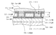
図1は、実施の形態1における半導体装置の一例を示す断面図である。
図1において、基体200上には、SiO2膜210が形成され、SiO2膜210上に第1の絶縁膜が形成されている。第1の絶縁膜としては、下地膜となるSiC膜212とSiC膜212上にlow−k膜220、low−k膜220上にSiO2膜222が形成される。第1の絶縁膜には、導電性材料としてCuを用いた高さRの複数のCu配線となるCu膜260と各Cu配線となるCu膜260側面及び下面を覆うバリアメタル膜240が形成される。ここで、前記Cu配線となるCu膜260の側面上端部と前記バリアメタル膜とが接触していない非接触領域としてリセス270が深さ方向にrの距離存在する。或いは/及び、リセス270として、前記Cu配線となるCu膜260の側面が前記バリアメタル膜240の側面に対し角度θ傾斜して接触していない領域を形成する。SiO2膜222、バリアメタル膜240の上端部、及びCu配線となるCu膜260上面には、SiC膜275が形成され、SiC膜275は、リセス270を埋めている。SiC膜275上には、多層配線のために次のlow−k膜280が形成される。
In the first embodiment, a method for solving the problem of the breakdown voltage degradation between narrow pitch Cu wirings by securing the distance of the region where the Cu film and the barrier metal film are not in contact with each other on the upper side wall of the damascene Cu wiring. Will be explained.
FIG. 1 is a cross-sectional view illustrating an example of the semiconductor device according to the first embodiment.
In FIG. 1, a SiO 2 film 210 is formed on a
上記の狭ピッチCu配線となるCu膜260間の絶縁耐圧劣化の問題は、ダマシンCu配線の側壁上部にリセス270を設け、このリセス270によってCu膜とバリアメタル膜の表面が接触していない距離を確保し、比誘電率が3.5のlow−k膜220の場合、その距離rが2nm以上であることにより解決される。さらに、リセス270の深さ方向の距離rが5nm以上であれば、比誘電率が2.9のlow−k膜がCMP面に露出していても絶縁耐圧が高く、10nm以上であれば、比誘電率が2.5のlow−k膜がCMP面に露出していても高い絶縁耐圧を確保することが可能となる。
The problem of the breakdown voltage degradation between the
若しくは、ダマシンCu配線となるCu膜260の側壁上部にリセス270を設けることによって、比誘電率が3.5のlow−k膜220の場合、前記Cu膜とバリアメタル膜の表面が、Cu配線の高さRの1/100以上の距離rだけ接触していないことにより解決される。さらに、リセスの深さの距離rがCu配線の高さRの1/50以上の距離だけ離れていれば、比誘電率が2.9のlow−k膜がCMP面に露出していても絶縁耐圧が高く、リセスの深さの距離rがCu配線の高さRの1/10以上の距離だけ離れていれば、比誘電率が2.5のlow−k膜がCMP面に露出していても高い絶縁耐圧を確保することが可能となる。
Alternatively, in the case of the low-
若しくは、ダマシンCu配線となるCu膜260の側壁上部において、比誘電率が3.5のlow−k膜220の場合、Cu膜表面とバリアメタル膜表面の角度θが5度以上の角度を有して離れていることが望ましい。さらに、10度以上の角度θを有して離れていれば、比誘電率が2.9のlow−k膜がCMP面に露出していても絶縁耐圧が高く、25度以上の角度θを有して離れていれば、比誘電率が2.5のlow−k膜がCMP面に露出していても高い絶縁耐圧を確保することが可能となる。かかる角度θと前記接触していない深さ方向の距離rとを両方備えていれば、なおよい。
Alternatively, in the case of the low-
以下、図1の半導体装置の製造方法を説明する。
図2は、図1の半導体装置の構成のうち、下層のSiO2膜形成工程からlow−k膜上のSiO2膜形成工程までを示す工程断面図である。それ以降の工程は後述する。
A method for manufacturing the semiconductor device of FIG. 1 will be described below.
2, of the structure of the semiconductor device of FIG. 1 is a process cross-sectional view showing a from the underlying SiO 2 film forming step to the SiO 2 film formation process on the low-k film. Subsequent steps will be described later.
図2(a)において、SiO2膜形成工程として、基体200上にCVD法によって、例えば、膜厚200nmの下地SiO2膜を堆積し、SiO2膜210を形成する。ここでは、CVD法によって成膜しているが、その他の方法を用いても構わない。基体200として、例えば、直径300ミリのシリコンウエハを用いる。ここでは、デバイス部分の形成を省略している。
In FIG. 2A, as the SiO 2 film forming step, for example, a base SiO 2 film having a film thickness of 200 nm is deposited on the
図2(b)において、SiC膜形成工程として、SiO2膜210の上に、CVD法によって、SiCを用いた膜厚30nmの下地SiC膜を堆積し、SiC膜212を形成する。ここでは、CVD法によって成膜しているが、その他の方法を用いても構わない。SiC膜212は、エッチングストッパとしての機能も有する。SiC膜を生成するのは難しいためSiC膜の代わりにSiOC膜を用いても構わない。或いは、SiCN膜、SiN膜を用いることができる。
In FIG. 2B, as a SiC film formation step, a
図2(c)において、low−k膜形成工程として、基体200の上に形成された前記SiC絶縁膜形成工程により形成されたSiC膜212の上に多孔質の絶縁性材料を用いたlow−k膜220を200nmの厚さで形成する。low−k膜220を形成することで、比誘電率kが3.5よりも低い層間絶縁膜を得ることができる。low−k膜220の材料としては、例えば、多孔質のメチルシルセスキオキサン(methyl silsequioxane:MSQ)を用いることができる。また、その形成方法としては、例えば、溶液をスピンコートし熱処理して薄膜を形成するSOD(spin on dielectic coating)法を用いることができる。ここでは、スピナーの回転数は900min−1(900rpm)で成膜した。このウエハをホットプレート上で窒素雰囲気中250℃の温度でベークを行い、最終的にホットプレート上で窒素雰囲気中450℃の温度で10分間のキュアを行った。MSQの材料や形成条件などを適宜調節することにより、所定の物性値を有する多孔質の絶縁膜が得られる。例えば、密度が0.7g/cm3で比誘電率kが1.8となる。low−k膜のSiとOとCの組成比は、Siが25から35%の範囲、Oが45から57%の範囲、Cが13から24%の範囲にある物性値を有するLow−k膜220が得られる。そして、Heプラズマ処理工程として、このlow−k膜220表面をCVD装置内でヘリウム(He)プラズマ照射によって表面改質する。Heプラズマ照射によって表面が改質されることで、low−k膜220とlow−k膜220上に形成する後述するキャップ膜としてのCVD−SiO2膜222との接着性を改善することができる。ガス流量は1.7Pa・m3/s(1000sccm)、ガス圧力は1000Pa、高周波パワーは500W、低周波パワーは400W、温度は400℃とした。キャップCVD膜をlow−k膜上に成膜する際は、low−k膜表面にプラズマ処理を施すことがキャップCVD膜との接着性を改善する上で有効である。プラズマガスの種類としてはアンモニア(NH3)、亜酸化窒素(N2O)、水素(H2)、He、酸素(O2)、シラン(SiH4)、アルゴン(Ar)、窒素(N2)などがあり、これらの中でもHeプラズマはlow−k膜へのダメージが少ないために特に有効である。また、プラズマガスはこれらのガスを混合したものでも良い。例えば、Heガスは他のガスと混合して用いると効果的である。
In FIG. 2C, as a low-k film forming step, a low-k using a porous insulating material on the
図2(d)において、SiO2膜形成工程として、前記Heプラズマ処理を行った後、キャップ膜として、CVD法によってlow−k膜220上にSiO2を膜厚50nm堆積することで、SiO2膜222を形成する。SiO2膜222を形成することで、直接リソグラフィを行うことができないlow−k膜220を保護し、low−k膜220にパターンを形成することができる。かかるキャップCVD膜は、SiO2膜、SiC膜、SiOC膜、SiCN膜などがあるが、ダメージ低減の観点からはSiO2膜が優れ、低誘電率化の観点からはSiOC膜が、耐圧向上の観点からはSiC膜やSiCN膜が優れている。さらに、SiO2膜とSiC膜の積層膜、もしくはSiO2膜とSiCO膜の積層膜、もしくはSiO2膜とSiCN膜の積層膜を用いることができる。さらにキャップCVD膜の一部、もしくは全てが後述する平坦化工程においてCMPにより除去されても良い。キャップ膜を除去することで誘電率をさらに低減することができる。キャップ膜の厚さとしては10nmから150nmが良く、10nmから50nmが実効的な比誘電率を低減する上で効果的である。
In FIG. 2 (d), the as SiO 2 film forming step, said after the He plasma treatment, as a cap film, the SiO 2 by a thickness of 50nm is deposited on the low-
以上の説明において、下層配線における層間絶縁膜は、比誘電率が3.5以下のlow−k膜でなくても構わないが、low−k膜を含む場合に特に有効である。なぜならば、low−k膜は絶縁耐圧が低い材料が多いだけでなく、CMPプロセスによりダメージを受けやすいからである。 In the above description, the interlayer insulating film in the lower layer wiring may not be a low-k film having a relative dielectric constant of 3.5 or less, but is particularly effective when a low-k film is included. This is because the low-k film is not only a material with a low withstand voltage but also easily damaged by the CMP process.
図3は、配線形成のための開口部形成工程からめっき工程までを示す工程断面図である。それ以降の工程は後述する。
図3(a)において、開口部形成工程として、リソグラフィ工程とドライエッチング工程でダマシン配線を作製するための配線溝構造である開口部150をSiO2膜222とlow−k膜220と下地SiC膜212内に形成する。図示していないレジスト塗布工程、露光工程等のリソグラフィ工程を経てSiO2膜222の上にレジスト膜が形成された基体200に対し、露出したSiO2膜222とその下層に位置するlow−k膜220を、下地SiC膜212をエッチングストッパとして異方性エッチング法により除去し、その後、下地SiC膜212をエッチングして開口部150を形成すればよい。異方性エッチング法を用いることで、基体200の表面に対し、略垂直に開口部150を形成することができる。例えば、一例として、反応性イオンエッチング法により開口部150を形成すればよい。
FIG. 3 is a process cross-sectional view illustrating the process from the opening forming process for wiring formation to the plating process. Subsequent steps will be described later.
In FIG. 3A, as the opening forming process, the opening 150 which is a wiring groove structure for producing a damascene wiring by a lithography process and a dry etching process is formed by using an SiO 2 film 222, a low-
図3(b)において、バリアメタル膜形成工程として、前記開口部形成工程により形成された開口部150及びSiO2膜222表面にバリアメタル材料を用いたバリアメタル膜240を形成する。物理気相成長法(physical vapor deposition:PVD)法の1つであるスパッタ法を用いるスパッタリング装置内で窒化タンタル(TaN)を膜厚2nm、原子層気相成長(atomic layer deposition:ALD法、あるいは、atomic layer chemical vapor deposition:ALCVD法)によりタンタル(Ta)膜を膜厚1nm堆積し、さらにその上にスパッタ法によるTa膜を膜厚2nm堆積し、バリアメタル膜240を形成する。TaN膜とTa膜とを積層することで、TaN膜によりCuのlow−k膜220への拡散防止を図り、Ta膜によりCuの密着性向上を図ることができる。バリアメタル材料の堆積方法としては、ALD法、ALCVD法やCVD法などを用いることでPVD法を用いる場合より被覆率を良くすることができる。
前記バリアメタル膜は、Ta膜、TaN膜、もしくはその積層膜であることが望ましい。前記バリアメタル膜の成膜方法は、CVD法もしくはALD法であることが被覆性の観点から望ましいが、上述したスパッタ法などのPVD法であっても有効である。
In FIG. 3B, as a barrier metal film forming step, a
The barrier metal film is preferably a Ta film, a TaN film, or a laminated film thereof. The film formation method of the barrier metal film is preferably a CVD method or an ALD method from the viewpoint of coverage, but is effective even with a PVD method such as the sputtering method described above.
図3(c)において、シード膜形成工程として、スパッタ等の物理気相成長(PVD)法により、次の工程である電解めっき工程のカソード極となるCu薄膜をシード膜250としてバリアメタル膜240が形成された開口部150内壁及び基体200表面に堆積(形成)させる。ここでは、シード膜250を膜厚75nm堆積させた。
In FIG. 3C, as a seed film forming process, a
図3(d)において、めっき工程として、シード膜250をカソード極として、電解めっき等の電気化学成長法によりCu膜260を開口部150及び基体200表面に堆積させる。ここでは、膜厚300nmのCu膜260を堆積させ、堆積させた後にアニール処理を250℃の温度で30分間行った。
In FIG. 3D, as a plating process, a
図4は、平坦化する研磨工程から図1に示す第2の絶縁膜としてのlow−k膜形成工程までを示す工程断面図である。 FIG. 4 is a process cross-sectional view showing a polishing process for planarization to a low-k film forming process as the second insulating film shown in FIG.
図4(a)において、研磨工程として、CMP法によってSiO2膜222の表面に堆積された導電部としての配線層となるCu膜260、シード膜250、及びバリアメタル膜240を研磨除去することにより、図4(a)に表したような埋め込み構造を形成する。ここでは、一例として、CMP装置はオービタル方式で、ノベラスシステムズ社のMomentum300を用いた。CMP荷重は1.03×10⁴Pa(1.5psi)、オービタル回転数は600min−1(600rpm)、ヘッド回転数は24min−1(24rpm)、スラリー供給速度は0.3L/min(300cc/分)、研磨パッドは発泡ポリウレタン製の単層パッド(ロデール社のIC1000)、CMPスラリーはCu用に砥粒フリースラリー(日立化成工業製のHS−C430−TU)、バリアメタル用にコロイダルシリカ砥粒スラリー(日立化成工業製のHS−T605−8)を用いた。上述の条件でCMPを行い、溝外部のCu膜とバリアメタル膜を除去してダマシンCu配線を形成した。
In FIG. 4A, as a polishing step, the
図4(b)において、エッチング工程として、前記研磨工程により研磨された基体表面を、エッチング液を用いてエッチングし、リセス270を形成する。CMP工程後、かつ後洗浄工程に入る直前に、エッチング液として、0.1%クエン酸と9%過酸化水素と0.5%ベンゾトリアゾール(BTA)が混合された水溶液を用いてリンスをCMPプラテン上において行なう。これにより図4(b)のようなCu配線の上端部にリセス270を形成する。例えば、30秒間リンスを行なうことにより、Cu配線の上端部に深さ方向の距離rが10nmのリセスを形成した。Cu膜260表面とバリアメタル膜240表面のリセス270部における角度θは、30度離れている。リンスを行わなかったウエハ(図13)も、比較試料(レファレンス)として、リンスを行ったウエハと電気特性を比較するため用意した。
In FIG. 4B, as the etching process, the substrate surface polished by the polishing process is etched using an etchant to form a recess 270. After the CMP step and immediately before entering the post-cleaning step, the rinse is performed using an aqueous solution in which 0.1% citric acid, 9% hydrogen peroxide, and 0.5% benzotriazole (BTA) are mixed as an etchant. Perform on the platen. Thereby, a recess 270 is formed at the upper end of the Cu wiring as shown in FIG. For example, by rinsing for 30 seconds, a recess having a depth direction distance r of 10 nm was formed at the upper end of the Cu wiring. The angle θ in the recess 270 between the
図5は、リセスを形成する装置の構成を説明するための概念図である。
図5(a)に示すように、CMPプロセスのステップの一部として、ロータリ型のCMP装置において、プラテン520上に配置された研磨パッド525上に、研磨面を下に向けて基板300をキャリア510が保持する。そして、スラリーを用いた研磨工程が終了後、研磨パッド525上のスラリーを純水にて流し、置換した後、前記エッチング液を供給液540として、供給ノズル530から供給する。図5(b)に示すように、キャリア510を図に示すように回転することで基板300を回転させ、プラテン520も回転させる。プラテン520の回転方向先に位置する基板300の手前(図5(b)の540に示す位置)に供給液540を供給することで、供給液540が基板300面内に供給される。
FIG. 5 is a conceptual diagram for explaining the configuration of an apparatus for forming a recess.
As shown in FIG. 5A, as part of the steps of the CMP process, in a rotary type CMP apparatus, the
或いは、次のようにリセスを形成してもよい。
図6は、リセスを形成する別の装置の構成を説明するための概念図である。
図6において、CMP直後のリンスプロセスのステップとして、回転テーブル720上に配置された4つの保持具710にて基板300を保持する。そして、回転軸760の回転により回転テーブル720が回転することで、基板300を回転させながら供給口730から供給液740を供給する。例えば、供給液740として、リンス洗浄として純水を15秒、その後、エッチング液を15秒、再度リンス洗浄として純水を30秒流す。エッチング液供給の際には、回転数200min−1(200rpm)で5×10⁻¹Pa・m3/s(300sccm)流す。
Alternatively, the recess may be formed as follows.
FIG. 6 is a conceptual diagram for explaining the configuration of another apparatus for forming a recess.
In FIG. 6, as a rinsing process step immediately after CMP, the
或いは、次のようにリセスを形成してもよい。
図7は、リセスを形成する別の装置の構成を説明するための概念図である。
図7において、CMP後洗浄プロセスのステップの一部として、回転テーブル620上に配置された4つの保持具610にて研磨された研磨面を上にして基板300を保持する。そして、回転軸660の回転により回転テーブル620が回転することで、基板300を回転させながら供給口630から供給液640を供給する。基板300表面は、回転軸656にて揺動可能なアーム654の先端部に配置された回転軸652により回転するブラシ650でブラシスクラブされる。例えば、供給液640として、リンス洗浄として純水を15秒、その後、エッチング液を15秒、再度エッチング液の洗浄として純水を30秒流す。エッチング液供給の際には、回転数100min−1(100rpm)で5×10⁻¹Pa・m3/s(300sccm)流す。
Alternatively, the recess may be formed as follows.
FIG. 7 is a conceptual diagram for explaining the configuration of another apparatus for forming a recess.
In FIG. 7, as part of the post-CMP cleaning process step, the
或いは、次のようにリセスを形成してもよい。
図8は、リセスを形成する別の装置の構成を説明するための概念図である。
CMP後洗浄プロセスのステップの一部として、図8(b)に示す保持具710にて研磨された研磨面を上にして基板300を保持する。そして、図示しない回転軸の回転により基板300を回転させながら供給口730は上面に向かって供給液740を供給し、供給口732は下面に向かって供給液742を供給する。図8(a)、(b)に示すように基板300表面は、自転するブラシ750とブラシ752とで挟持されブラシスクラブされる。例えば、図7と同様、供給液640として、リンス洗浄として純水を15秒、その後、エッチング液を30秒、再度リンス洗浄として純水を30秒流す。エッチング液供給の際には、回転数100min−1(100rpm)で5×10⁻¹Pa・m3/s(300sccm)流す。ここでは、研磨面(リセスを形成する面)を上向きにしているが、下向きにしても構わない。その場合は、供給液742として、エッチング液を流せばよい。
Alternatively, the recess may be formed as follows.
FIG. 8 is a conceptual diagram for explaining the configuration of another apparatus for forming a recess.
As part of the post-CMP cleaning process step, the
或いは、次のようにリセスを形成してもよい。
図9は、リセスを形成する別の装置の構成を説明するための概念図である。
図9(a)に示すように、CMPプロセスのステップの一部として、オービタル回転型のCMP装置において、プラテン820上に配置された研磨パッド825上に、研磨面を下に向けて基板300をキャリア810が保持する。そして、スラリーを用いた研磨工程が終了後、研磨パッド825上のスラリーを純水にて流し、置換した後、プラテン820を図に示すようにオービタル回転させながら、図9(b)に示すように、前記エッチング液を供給液840として、研磨パッド825の下側から供給する。供給液840を研磨パッド825の下側から供給することで、供給液840が基板300面内に供給される。供給された供給液840は、プラテン820の回転に伴い、外周部から排出される。
Alternatively, the recess may be formed as follows.
FIG. 9 is a conceptual diagram for explaining the configuration of another apparatus for forming a recess.
As shown in FIG. 9A, as part of the steps of the CMP process, in an orbital rotating CMP apparatus, the
以上のように、これらのリセス構造を形成は、CMPプロセスのステップの一部、CMP直後のリンスプロセスのステップ、CMP後洗浄プロセスのステップの一部にエッチング剤を用いることによって達成できる。図5や図9に示すように、CMPプラテン上でエッチング液を流しながら研磨面をリンスすることによっても可能であるし、図7や図8に示すように後洗浄プロセスにおいてブラシスクラブをしながらエッチング液を流すことによっても可能である。単に、エッチング液に浸漬させても可能である。エッチング液は酸化剤と有機酸の混合水溶液が望ましい。酸化剤としては過酸化水素、有機酸としてはヒドロキシ酸(OH基を含む有機酸)もしくはカルボン酸(COOH基を含む有機酸)が望ましく、ヒドロキシカルボン酸(OH基とCOOH基を一分子中に含む有機酸)が最も望ましい。例えば、クエン酸、リンゴ酸、コハク酸、酒石酸、フタル酸、マロン酸、マレイン酸、フマル酸、乳酸、ピメリン酸、アジピン酸、グルタル酸、シュウ酸、サリチル酸、グルコール酸、安息香酸、酪酸、吉草酸、プロピオン酸、酢酸、ギ酸などが挙げられる。薬品の濃度は前述の距離、角度になるように最適化することが可能である。有機酸の濃度としては0.01から1%の範囲内で最適化ができる。酸化剤の濃度としては1から30%の範囲内で最適化できる。
エッチングの深さを制御するために、さらに防食剤や界面活性剤を添加することは有効である。防食剤としてはベイゾトリアゾール(BTA)やイミダゾール、もしくはその誘導体が望ましい。界面活性剤としては、ポリアクリル酸もしくはポリアクリル酸アンモニウムが望ましい。防食剤の濃度としては0.01から0.5%の範囲内で最適化ができる。界面活性剤の濃度としては0.001から1%の範囲内で最適化できる。
As described above, the formation of these recess structures can be achieved by using an etchant as a part of a CMP process step, a rinse process step immediately after CMP, and a post-CMP cleaning process step. As shown in FIGS. 5 and 9, it is also possible to rinse the polishing surface while flowing an etching solution on the CMP platen, or while brush scrubbing in the post-cleaning process as shown in FIGS. It is also possible by flowing an etching solution. It is also possible to simply immerse in an etching solution. The etching solution is preferably a mixed aqueous solution of an oxidizing agent and an organic acid. The oxidizing agent is preferably hydrogen peroxide, and the organic acid is preferably a hydroxy acid (an organic acid containing an OH group) or a carboxylic acid (an organic acid containing a COOH group), and the hydroxycarboxylic acid (an OH group and a COOH group in one molecule). Organic acids) are most desirable. For example, citric acid, malic acid, succinic acid, tartaric acid, phthalic acid, malonic acid, maleic acid, fumaric acid, lactic acid, pimelic acid, adipic acid, glutaric acid, oxalic acid, salicylic acid, glucholic acid, benzoic acid, butyric acid, Yoshi Examples include herbic acid, propionic acid, acetic acid, formic acid and the like. The concentration of the chemical can be optimized so as to be the above-mentioned distance and angle. The concentration of the organic acid can be optimized within the range of 0.01 to 1%. The concentration of the oxidizing agent can be optimized within a range of 1 to 30%.
In order to control the depth of etching, it is effective to add an anticorrosive or a surfactant. As the anticorrosive agent, beizotriazole (BTA), imidazole, or a derivative thereof is desirable. As the surfactant, polyacrylic acid or ammonium polyacrylate is desirable. The concentration of the anticorrosive can be optimized within the range of 0.01 to 0.5%. The surfactant concentration can be optimized within the range of 0.001 to 1%.
図4(c)において、還元性プラズマ処理工程として、CVD装置内でアンモニア(NH3)プラズマ処理を行なう。この処理により図4(a)における平坦化工程でのCu−CMPの際にスラリーとの反応によって形成されたCu表面の錯体を還元し、キャップSiO2膜上に存在する残留有機物を除去することができる。この処理によりCu−CMPの際にスラリーとの反応によって形成されたCu表面の錯体が還元され、キャップSiO2膜上にある残留有機物も除去されることから絶縁耐圧は改善される。前記還元性のプラズマはアンモニアプラズマ、もしくは水素(H2)プラズマが効果的であり、特にアンモニアプラズマが処理装置内におけるガスの扱い易さから好ましい。
In FIG. 4C, ammonia (NH 3 ) plasma treatment is performed in the CVD apparatus as a reducing plasma treatment step. By this treatment, the Cu surface complex formed by the reaction with the slurry during Cu-CMP in the planarization step in FIG. 4A is reduced, and the residual organic substances present on the cap SiO 2 film are removed. Can do. By this treatment, the Cu surface complex formed by reaction with the slurry during Cu-CMP is reduced, and residual organic substances on the
還元性プラズマ処理工程では、図示していないCVD装置内におけるチャンバの内部にて、下部電極を兼ねた温度が400℃に制御された基板ホルダの上に基体200となる半導体基板を設置する。そして、チャンバの内部に上部電極内部からガスを供給する。供給するガス流量は11.8Pa・m3/s(7000sccm)とした。真空ポンプにより233Paのガス圧力になるように真空引きされたチャンバの内部の上記上部電極と下部電極との間に高周波電源を用いてプラズマを生成させる。高周波パワーは560W、低周波パワーは250W、処理時間は10秒とした。
In the reducing plasma processing step, a semiconductor substrate serving as the
そして、次の層における第2の絶縁膜形成工程の一部であるSiC膜形成工程として、還元性プラズマ処理した同じCVD装置内で400℃の温度で30nmの膜厚のSiC膜275を形成する。SiC膜275は、リセス270にも埋め込まれる。SiC膜275は拡散防止膜の働きがあり、このSiC膜275を形成することで、Cuの拡散を防止することができる。かかるCVD法で形成されるSiC膜275の他に、SiCN膜、SiCO膜、SiN膜、SiO2膜を用いることができる。
Then, as the SiC film forming process which is a part of the second insulating film forming process in the next layer, an
図4(d)において、low−k膜形成工程として、図2(c)で説明した工程と同様に、SiC膜275の上にSiC膜275よりも比誘電率の低い低誘電率膜である、多孔質の絶縁性材料を用いたlow−k膜280を形成する。以降、多層配線を必要に応じ順次形成する。
In FIG. 4D, the low-k film forming process is a low dielectric constant film having a relative dielectric constant lower than that of the
これらリセスを形成したウエハと形成していないウエハとの2種類のウエハに保護膜とパッド電極を形成して、Cu配線間の絶縁耐圧試験を行った。前述の2種類のウエハにおいて、Cu配線の幅が0.13マイクロメートル、配線間のスペースが0.13マイクロメートルの構造において絶縁耐圧を調べた。その結果、本発明のリンス処理を行ったウエハでは絶縁耐圧の劣化はほとんど見られなかった。99%以上の歩留りで、2MV/cm以上の耐圧があった。これに対して、前述のリンス処理(リセス形成)を行っていないウエハでは同一配線構造の絶縁耐圧が50%まで低下した。劣化したCu配線をTEMで観察した結果、図15に示すような破壊が見られた。すなわち、Cu上端部から絶縁破壊が起こっていた。一方、リンス処理(リセス形成)を行ったウエハでは絶縁破壊が見つからなかった。つまり、リンス処理されたウエハでは配線上端部におけるCuの電界拡散が防止され、絶縁破壊電圧の低下を抑制することができたものと考えられる。 A protective film and a pad electrode were formed on two types of wafers, a wafer having these recesses and a wafer having no recesses, and a dielectric strength test between Cu wirings was performed. With respect to the above-described two types of wafers, the withstand voltage was examined in a structure in which the width of the Cu wiring was 0.13 micrometers and the space between the wirings was 0.13 micrometers. As a result, the dielectric breakdown voltage was hardly deteriorated in the wafer subjected to the rinsing process of the present invention. With a yield of 99% or more, there was a breakdown voltage of 2MV / cm or more. On the other hand, the withstand voltage of the same wiring structure was reduced to 50% in the wafer not subjected to the above-described rinsing (recess formation). As a result of observing the deteriorated Cu wiring with TEM, breakdown as shown in FIG. 15 was observed. That is, dielectric breakdown occurred from the upper end of Cu. On the other hand, no dielectric breakdown was found in the wafer subjected to the rinsing process (recess formation). In other words, it is considered that the rinsed wafer prevented the electric field diffusion of Cu at the upper end portion of the wiring and suppressed the breakdown voltage.
図10は、CMPのダメージ層とCu膜の上端部の距離がリセスによって離れることを説明するための概念図である。
絶縁破壊電圧の低下を抑制することができたのは、図10に示すように、CMPのダメージ層とCu膜の上端部の距離がリセスによって離れることで、Cuの電界拡散が抑制されたものと考えられる。
図11は、リセスの深さと絶縁耐圧の関係を調べた結果を示す図である。
リセスの深さと絶縁耐圧の関係を調べた結果、リセスの深さが2nm以上あると有効であることがわかった。さらに5nm以上あれば効果が絶大であった。リセスが20nm以上になると、絶縁耐性の効果は高くなるが、配線抵抗の増加が無視できなくなるという問題があることから、リセスの深さがCu配線の高さの1/100以上、1/5以下であることが望ましい。Cu配線の上端部にある場合は、Cu膜表面とバリアメタル膜表面が5度以上の角度を有して離れていることが望ましい。
本実験をデバイスが搭載されたウエハで実施しても同様の効果を確認することができた。1層目のCu配線層だけでなく、2層目のCu配線層においても有効であり、さらに3層目以上のCu配線層でも有効な結果が得られた。
low−k材料としては、HSQ(Hydrogen Silsesquioxane)やポリマー、CVDで形成されたSiOC膜を用いても同様の結果が得られた。
FIG. 10 is a conceptual diagram for explaining that the distance between the damaged layer of CMP and the upper end of the Cu film is separated by the recess.
As shown in FIG. 10, the decrease in the dielectric breakdown voltage can be suppressed because the distance between the CMP damage layer and the upper end of the Cu film is separated by the recess, thereby suppressing the Cu electric field diffusion. it is conceivable that.
FIG. 11 is a diagram showing the results of examining the relationship between the recess depth and the withstand voltage.
As a result of investigating the relationship between the depth of the recess and the withstand voltage, it has been found that it is effective that the depth of the recess is 2 nm or more. Further, if the thickness was 5 nm or more, the effect was great. If the recess is 20 nm or more, the effect of insulation resistance is enhanced, but there is a problem that an increase in wiring resistance cannot be ignored. Therefore, the depth of the recess is 1/100 or more of the height of the Cu wiring, and 1/5. The following is desirable. In the case of the upper end portion of the Cu wiring, it is desirable that the Cu film surface and the barrier metal film surface be separated from each other with an angle of 5 degrees or more.
The same effect could be confirmed even when this experiment was carried out on a wafer with a device mounted. This is effective not only in the first Cu wiring layer but also in the second Cu wiring layer, and also in the third and higher Cu wiring layers.
As the low-k material, the same result was obtained even when using a SiOC film formed by HSQ (Hydrogen Silsesquioxane), polymer, or CVD.
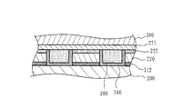
実施の形態2.
図12は、実施の形態2における半導体装置の一例を示す断面図である。
図12に示すように、リセス270の形状は、Cu配線となるCu膜260の上端部であっても、Cu配線となるCu膜260の表面全体に及んでいても良い。
FIG. 12 is a cross-sectional view illustrating an example of the semiconductor device in the second embodiment.
As shown in FIG. 12, the shape of the recess 270 may extend over the entire surface of the
前記各実施の形態において、比誘電率kが2.6以下の場合、low−k膜の側壁が、20nm以下の膜厚のCVD膜で被覆されていることが望ましい。その理由は、比誘電率が2.6以下の場合はポーラス膜であることが多く、ポアシーリングをCu配線の側壁で行う必要があるからである。特に、前述のALD法やCVD法によってバリアメタル膜を成膜する場合は必要である。ポアシーリング用のCVD膜の種類としては、SiC膜、SiCN膜、SiCO膜、SiN膜が望ましい。特に、低誘電率の観点からSiC膜が最適である。 In each of the above embodiments, when the relative dielectric constant k is 2.6 or less, it is desirable that the sidewall of the low-k film is covered with a CVD film having a thickness of 20 nm or less. The reason is that when the relative dielectric constant is 2.6 or less, the film is often a porous film, and pore sealing needs to be performed on the side wall of the Cu wiring. This is particularly necessary when a barrier metal film is formed by the aforementioned ALD method or CVD method. As the kind of the pore sealing CVD film, a SiC film, a SiCN film, a SiCO film, and a SiN film are desirable. In particular, a SiC film is optimal from the viewpoint of a low dielectric constant.
以上の説明において、前記各実施の形態は、配線ピッチが300nm以下であると特に有効である。200nm以下であるとさらに有効である。配線ピッチが小さくなるほど絶縁破壊の問題は大きくなり、前記各実施の形態は、配線ピッチが小さくなるほど有効となる。 In the above description, the above embodiments are particularly effective when the wiring pitch is 300 nm or less. It is more effective when it is 200 nm or less. As the wiring pitch decreases, the problem of dielectric breakdown increases, and the above-described embodiments become more effective as the wiring pitch decreases.
以上の説明において、バリアメタルとして、Ta、TaNに限らず、TaCN(炭化窒化タンタル)、WN(窒化タングステン)、WCN(炭化窒化タングステン)、TiN(窒化チタン)等の高融点金属の窒化膜或いは窒化炭素膜であっても構わない。或いはチタン(Ti)、WSiN等であっても構わない。 In the above description, the barrier metal is not limited to Ta and TaN, but a nitride film of a refractory metal such as TaCN (tantalum carbonitride), WN (tungsten nitride), WCN (tungsten carbonitride), or TiN (titanium nitride) A carbon nitride film may be used. Alternatively, titanium (Ti), WSiN, or the like may be used.
ここで、上記各実施の形態における配線層の材料として、Cu以外に、Cu−Sn合金、Cu−Ti合金、Cu−Al合金等の、半導体産業で用いられるCuを主成分とする材料を用いて同様の効果が得られる。 Here, as a material of the wiring layer in each of the above embodiments, a material mainly containing Cu used in the semiconductor industry, such as a Cu—Sn alloy, a Cu—Ti alloy, and a Cu—Al alloy, is used in addition to Cu. The same effect can be obtained.
なお、多層配線構造などを形成する場合には、各図において基体200は、下層の配線層と絶縁膜とが形成されたものである。
In the case of forming a multilayer wiring structure or the like, the
上記各実施の形態においては、多孔質絶縁膜の材料としては、多孔質誘電体薄膜材料としてのMSQに限らず、他の多孔質無機絶縁体膜材料、多孔質有機絶縁体膜材料を用いても同様の効果を得ることができる。
特に、多孔質の低誘電率材料に上記各実施の形態を適用した場合には、上述の如く顕著な効果が得られる。上記各実施の形態において多孔質絶縁膜の材料として用いることができるものとしては、例えば、各種のシルセスキオキサン化合物、ポリイミド、炭化フッ素(fluorocarbon)、パリレン(parylene)、ベンゾシクロブテンをはじめとする各種の絶縁性材料を挙げることができる。
In each of the embodiments described above, the material of the porous insulating film is not limited to the MSQ as the porous dielectric thin film material, and other porous inorganic insulating film materials and porous organic insulating film materials are used. The same effect can be obtained.
In particular, when the above-described embodiments are applied to a porous low dielectric constant material, a remarkable effect can be obtained as described above. Examples of materials that can be used as the material for the porous insulating film in each of the above embodiments include various silsesquioxane compounds, polyimide, fluorocarbon, parylene, benzocyclobutene, and the like. Various insulating materials can be mentioned.
以上、具体例を参照しつつ各実施の形態について説明した。しかし、本発明は、これらの具体例に限定されるものではない。 The embodiments have been described above with reference to specific examples. However, the present invention is not limited to these specific examples.
例えば、各実施の形態で層間絶縁膜が形成された基体200は、図示しない各種の半導体素子あるいは構造を有するものとすることができる。また、半導体基板ではなく、層間絶縁膜と配線層とを有する配線構造の上に、さらに層間絶縁膜を形成してもよい。開口部も半導体基板が露出するように形成してもよいし、配線構造の上に形成してもよい。
For example, the
さらに、層間絶縁膜の膜厚や、開口部のサイズ、形状、数などについても、半導体集積回路や各種の半導体素子において必要とされるものを適宜選択して用いることができる。 Further, the film thickness of the interlayer insulating film and the size, shape, number, and the like of the opening can be appropriately selected from those required in the semiconductor integrated circuit and various semiconductor elements.
その他、本発明の要素を具備し、当業者が適宜設計変更しうる全ての半導体装置の製造方法は、本発明の範囲に包含される。 In addition, any semiconductor device manufacturing method that includes the elements of the present invention and whose design can be changed as appropriate by those skilled in the art is included in the scope of the present invention.
また、説明の簡便化のために、半導体産業で通常用いられる手法、例えば、フォトリソグラフィプロセス、処理前後のクリーニング等は省略しているが、それらの手法が含まれることは言うまでもない。 In addition, for the sake of simplicity of explanation, techniques usually used in the semiconductor industry, such as a photolithography process, cleaning before and after processing, are omitted, but it goes without saying that these techniques are included.
150 開口部
200 基体
210,222 SiO2膜
212,275 SiC膜
220,280 low−k膜
221,281 絶縁膜
240 バリアメタル膜
250 シード膜
260 Cu膜
270 リセス
300 基板
510,810 キャリア
520,820 プラテン
525,825 研磨パッド
530 供給ノズル
540,640,740,742,840 供給液
610,710 保持具
620,720 回転テーブル
630,730 供給口
650,750,752 ブラシ
652,656,660,760 回転軸
654 アーム
150
Claims (9)
前記複数の導電部の各側面に配置されたバリアメタル膜と、
前記複数の導電部の間に、前記バリアメタル膜を介して配置された絶縁膜と、
を備え、
前記導電部の側面と前記バリアメタル膜とが接触していない領域が2nm以上の距離存在することを特徴とする半導体装置。 A plurality of conductive parts using a conductive material;
A barrier metal film disposed on each side surface of the plurality of conductive portions;
An insulating film disposed between the plurality of conductive portions via the barrier metal film;
With
A semiconductor device characterized in that a region where the side surface of the conductive portion and the barrier metal film are not in contact exists at a distance of 2 nm or more.
前記複数の導電部の各側面に配置されたバリアメタル膜と、
前記複数の導電部の間に、前記バリアメタル膜を介して配置された絶縁膜と、
を備え、
前記導電部の側面と前記バリアメタル膜とが接触していない領域が前記導電部の高さの1/100以上の距離存在することを特徴とする半導体装置。 A plurality of conductive parts using a conductive material;
A barrier metal film disposed on each side surface of the plurality of conductive portions;
An insulating film disposed between the plurality of conductive portions via the barrier metal film;
With
A region where the side surface of the conductive portion and the barrier metal film are not in contact exists at a distance of 1/100 or more of the height of the conductive portion.
前記複数の導電部の各側面に配置されたバリアメタル膜と、
前記複数の導電部の間に、前記バリアメタル膜を介して配置された絶縁膜と、
を備え、
前記導電部の側面が前記バリアメタル膜の側面に対し5度以上傾斜して接触していない領域を有することを特徴とする半導体装置。 A plurality of conductive parts using a conductive material;
A barrier metal film disposed on each side surface of the plurality of conductive portions;
An insulating film disposed between the plurality of conductive portions via the barrier metal film;
With
2. A semiconductor device according to claim 1, wherein a side surface of the conductive portion has a region which is not in contact with the side surface of the barrier metal film with an inclination of 5 degrees or more.
前記絶縁膜に開口部を形成する開口部形成工程と、
前記開口部の表面にバリアメタル膜を形成するバリアメタル膜形成工程と、
前記バリアメタル膜が表面に形成された前記開口部に導電性材料を堆積させる堆積工程と、
前記導電性材料が堆積した基体表面を研磨する研磨工程と、
前記研磨工程により研磨された基体表面を、エッチング液を用いてエッチングするエッチング工程と、
前記エッチング工程によりエッチングされた基体表面に絶縁膜を形成する第2の絶縁膜形成工程と、
を備えたことを特徴とする半導体装置の製造方法。 A first insulating film forming step of forming an insulating film on the substrate;
An opening forming step of forming an opening in the insulating film;
A barrier metal film forming step of forming a barrier metal film on the surface of the opening;
A deposition step of depositing a conductive material in the opening in which the barrier metal film is formed on the surface;
A polishing step of polishing the substrate surface on which the conductive material is deposited;
An etching step of etching the substrate surface polished by the polishing step using an etching solution;
A second insulating film forming step of forming an insulating film on the substrate surface etched by the etching step;
A method for manufacturing a semiconductor device, comprising:
Priority Applications (1)
| Application Number | Priority Date | Filing Date | Title |
|---|---|---|---|
| JP2004159070A JP2005340602A (en) | 2004-05-28 | 2004-05-28 | Semiconductor device and its fabrication process |
Applications Claiming Priority (1)
| Application Number | Priority Date | Filing Date | Title |
|---|---|---|---|
| JP2004159070A JP2005340602A (en) | 2004-05-28 | 2004-05-28 | Semiconductor device and its fabrication process |
Publications (1)
| Publication Number | Publication Date |
|---|---|
| JP2005340602A true JP2005340602A (en) | 2005-12-08 |
Family
ID=35493805
Family Applications (1)
| Application Number | Title | Priority Date | Filing Date |
|---|---|---|---|
| JP2004159070A Pending JP2005340602A (en) | 2004-05-28 | 2004-05-28 | Semiconductor device and its fabrication process |
Country Status (1)
| Country | Link |
|---|---|
| JP (1) | JP2005340602A (en) |
Cited By (2)
| Publication number | Priority date | Publication date | Assignee | Title |
|---|---|---|---|---|
| JP2007311560A (en) * | 2006-05-18 | 2007-11-29 | Toshiba Corp | Semiconductor device |
| JP2019220690A (en) * | 2018-06-15 | 2019-12-26 | 東京エレクトロン株式会社 | Method for protecting low-k layer |
-
2004
- 2004-05-28 JP JP2004159070A patent/JP2005340602A/en active Pending
Cited By (3)
| Publication number | Priority date | Publication date | Assignee | Title |
|---|---|---|---|---|
| JP2007311560A (en) * | 2006-05-18 | 2007-11-29 | Toshiba Corp | Semiconductor device |
| JP2019220690A (en) * | 2018-06-15 | 2019-12-26 | 東京エレクトロン株式会社 | Method for protecting low-k layer |
| JP7142607B2 (en) | 2018-06-15 | 2022-09-27 | 東京エレクトロン株式会社 | How to protect the low-k layer |
Similar Documents
| Publication | Publication Date | Title |
|---|---|---|
| JP3805588B2 (en) | Manufacturing method of semiconductor device | |
| US6890846B2 (en) | Method for manufacturing semiconductor integrated circuit device | |
| KR20030089474A (en) | Method of manufacturing semiconductor device and semiconductor device | |
| KR20030014123A (en) | Fabrication method of semiconductor integrated circuit device | |
| JP2001156029A (en) | Post-CuCMP for less defects | |
| US20110059607A1 (en) | Semiconductor device manufacturing method | |
| US10497614B2 (en) | Semiconductor structure and fabrication method thereof | |
| US20040121583A1 (en) | Method for forming capping barrier layer over copper feature | |
| US7202160B2 (en) | Method of forming an insulating structure having an insulating interlayer and a capping layer and method of forming a metal wiring structure using the same | |
| JP4864402B2 (en) | Manufacturing method of semiconductor device | |
| US10879114B1 (en) | Conductive fill | |
| JP3904578B2 (en) | Manufacturing method of semiconductor device | |
| US6436832B1 (en) | Method to reduce polish initiation time in a polish process | |
| TW202324735A (en) | Barrier schemes for metallization using manganese and graphene | |
| US7172963B2 (en) | Manufacturing method of semiconductor integrated circuit device that includes chemically and mechanically polishing two conductive layers using two polishing pads that have different properties | |
| JP2006140240A (en) | Polishing pad, polishing device, and method of manufacturing semiconductor device | |
| JP2005340460A (en) | Process for forming semiconductor device | |
| JP2005340601A (en) | Semiconductor device manufacturing method and semiconductor device | |
| TW201737343A (en) | Method of manufacturing a semiconductor device | |
| JP2005340602A (en) | Semiconductor device and its fabrication process | |
| JP4746443B2 (en) | Manufacturing method of electronic parts | |
| JP2006156519A (en) | Method of manufacturing semiconductor device | |
| JP2006120664A (en) | Method for manufacturing semiconductor device | |
| JP2011252218A (en) | Method for fabricating electronic component and electro-plating apparatus | |
| JP2006147653A (en) | Method of manufacturing semiconductor device |