EP3618101A1 - Sensor device and manufacturing method thereof - Google Patents
Sensor device and manufacturing method thereof Download PDFInfo
- Publication number
- EP3618101A1 EP3618101A1 EP18192054.7A EP18192054A EP3618101A1 EP 3618101 A1 EP3618101 A1 EP 3618101A1 EP 18192054 A EP18192054 A EP 18192054A EP 3618101 A1 EP3618101 A1 EP 3618101A1
- Authority
- EP
- European Patent Office
- Prior art keywords
- sensor element
- subframe
- volume
- elongate sensor
- package
- Prior art date
- Legal status (The legal status is an assumption and is not a legal conclusion. Google has not performed a legal analysis and makes no representation as to the accuracy of the status listed.)
- Pending
Links
Images


Classifications
-
- H—ELECTRICITY
- H10—SEMICONDUCTOR DEVICES; ELECTRIC SOLID-STATE DEVICES NOT OTHERWISE PROVIDED FOR
- H10W—GENERIC PACKAGES, INTERCONNECTIONS, CONNECTORS OR OTHER CONSTRUCTIONAL DETAILS OF DEVICES COVERED BY CLASS H10
- H10W90/00—Package configurations
- H10W90/811—Multiple chips on leadframes
-
- H—ELECTRICITY
- H10—SEMICONDUCTOR DEVICES; ELECTRIC SOLID-STATE DEVICES NOT OTHERWISE PROVIDED FOR
- H10W—GENERIC PACKAGES, INTERCONNECTIONS, CONNECTORS OR OTHER CONSTRUCTIONAL DETAILS OF DEVICES COVERED BY CLASS H10
- H10W74/00—Encapsulations, e.g. protective coatings
- H10W74/10—Encapsulations, e.g. protective coatings characterised by their shape or disposition
- H10W74/111—Encapsulations, e.g. protective coatings characterised by their shape or disposition the semiconductor body being completely enclosed
- H10W74/114—Encapsulations, e.g. protective coatings characterised by their shape or disposition the semiconductor body being completely enclosed by a substrate and the encapsulations
-
- H—ELECTRICITY
- H10—SEMICONDUCTOR DEVICES; ELECTRIC SOLID-STATE DEVICES NOT OTHERWISE PROVIDED FOR
- H10W—GENERIC PACKAGES, INTERCONNECTIONS, CONNECTORS OR OTHER CONSTRUCTIONAL DETAILS OF DEVICES COVERED BY CLASS H10
- H10W95/00—Packaging processes not covered by the other groups of this subclass
-
- G—PHYSICS
- G01—MEASURING; TESTING
- G01L—MEASURING FORCE, STRESS, TORQUE, WORK, MECHANICAL POWER, MECHANICAL EFFICIENCY, OR FLUID PRESSURE
- G01L1/00—Measuring force or stress, in general
- G01L1/18—Measuring force or stress, in general using properties of piezo-resistive materials, i.e. materials of which the ohmic resistance varies according to changes in magnitude or direction of force applied to the material
-
- G—PHYSICS
- G01—MEASURING; TESTING
- G01L—MEASURING FORCE, STRESS, TORQUE, WORK, MECHANICAL POWER, MECHANICAL EFFICIENCY, OR FLUID PRESSURE
- G01L19/00—Details of, or accessories for, apparatus for measuring steady or quasi-steady pressure of a fluent medium insofar as such details or accessories are not special to particular types of pressure gauges
- G01L19/0061—Electrical connection means
- G01L19/0069—Electrical connection means from the sensor to its support
- G01L19/0076—Electrical connection means from the sensor to its support using buried connections
-
- G—PHYSICS
- G01—MEASURING; TESTING
- G01L—MEASURING FORCE, STRESS, TORQUE, WORK, MECHANICAL POWER, MECHANICAL EFFICIENCY, OR FLUID PRESSURE
- G01L9/00—Measuring steady of quasi-steady pressure of fluid or fluent solid material by electric or magnetic pressure-sensitive elements; Transmitting or indicating the displacement of mechanical pressure-sensitive elements, used to measure the steady or quasi-steady pressure of a fluid or fluent solid material, by electric or magnetic means
- G01L9/0041—Transmitting or indicating the displacement of flexible diaphragms
- G01L9/0042—Constructional details associated with semiconductive diaphragm sensors, e.g. etching, or constructional details of non-semiconductive diaphragms
- G01L9/0045—Diaphragm associated with a buried cavity
-
- H—ELECTRICITY
- H10—SEMICONDUCTOR DEVICES; ELECTRIC SOLID-STATE DEVICES NOT OTHERWISE PROVIDED FOR
- H10W—GENERIC PACKAGES, INTERCONNECTIONS, CONNECTORS OR OTHER CONSTRUCTIONAL DETAILS OF DEVICES COVERED BY CLASS H10
- H10W70/00—Package substrates; Interposers; Redistribution layers [RDL]
- H10W70/40—Leadframes
- H10W70/421—Shapes or dispositions
-
- H—ELECTRICITY
- H10—SEMICONDUCTOR DEVICES; ELECTRIC SOLID-STATE DEVICES NOT OTHERWISE PROVIDED FOR
- H10W—GENERIC PACKAGES, INTERCONNECTIONS, CONNECTORS OR OTHER CONSTRUCTIONAL DETAILS OF DEVICES COVERED BY CLASS H10
- H10W70/00—Package substrates; Interposers; Redistribution layers [RDL]
- H10W70/60—Insulating or insulated package substrates; Interposers; Redistribution layers
- H10W70/67—Insulating or insulated package substrates; Interposers; Redistribution layers characterised by their insulating layers or insulating parts
- H10W70/68—Shapes or dispositions thereof
-
- H—ELECTRICITY
- H10—SEMICONDUCTOR DEVICES; ELECTRIC SOLID-STATE DEVICES NOT OTHERWISE PROVIDED FOR
- H10W—GENERIC PACKAGES, INTERCONNECTIONS, CONNECTORS OR OTHER CONSTRUCTIONAL DETAILS OF DEVICES COVERED BY CLASS H10
- H10W72/00—Interconnections or connectors in packages
- H10W72/071—Connecting or disconnecting
- H10W72/073—Connecting or disconnecting of die-attach connectors
-
- H—ELECTRICITY
- H10—SEMICONDUCTOR DEVICES; ELECTRIC SOLID-STATE DEVICES NOT OTHERWISE PROVIDED FOR
- H10W—GENERIC PACKAGES, INTERCONNECTIONS, CONNECTORS OR OTHER CONSTRUCTIONAL DETAILS OF DEVICES COVERED BY CLASS H10
- H10W72/00—Interconnections or connectors in packages
- H10W72/071—Connecting or disconnecting
- H10W72/075—Connecting or disconnecting of bond wires
-
- H—ELECTRICITY
- H10—SEMICONDUCTOR DEVICES; ELECTRIC SOLID-STATE DEVICES NOT OTHERWISE PROVIDED FOR
- H10W—GENERIC PACKAGES, INTERCONNECTIONS, CONNECTORS OR OTHER CONSTRUCTIONAL DETAILS OF DEVICES COVERED BY CLASS H10
- H10W74/00—Encapsulations, e.g. protective coatings
- H10W74/01—Manufacture or treatment
-
- H—ELECTRICITY
- H10—SEMICONDUCTOR DEVICES; ELECTRIC SOLID-STATE DEVICES NOT OTHERWISE PROVIDED FOR
- H10W—GENERIC PACKAGES, INTERCONNECTIONS, CONNECTORS OR OTHER CONSTRUCTIONAL DETAILS OF DEVICES COVERED BY CLASS H10
- H10W74/00—Encapsulations, e.g. protective coatings
- H10W74/10—Encapsulations, e.g. protective coatings characterised by their shape or disposition
- H10W74/111—Encapsulations, e.g. protective coatings characterised by their shape or disposition the semiconductor body being completely enclosed
-
- H—ELECTRICITY
- H10—SEMICONDUCTOR DEVICES; ELECTRIC SOLID-STATE DEVICES NOT OTHERWISE PROVIDED FOR
- H10W—GENERIC PACKAGES, INTERCONNECTIONS, CONNECTORS OR OTHER CONSTRUCTIONAL DETAILS OF DEVICES COVERED BY CLASS H10
- H10W72/00—Interconnections or connectors in packages
- H10W72/071—Connecting or disconnecting
- H10W72/075—Connecting or disconnecting of bond wires
- H10W72/07541—Controlling the environment, e.g. atmosphere composition or temperature
- H10W72/07554—Controlling the environment, e.g. atmosphere composition or temperature changes in dispositions
-
- H—ELECTRICITY
- H10—SEMICONDUCTOR DEVICES; ELECTRIC SOLID-STATE DEVICES NOT OTHERWISE PROVIDED FOR
- H10W—GENERIC PACKAGES, INTERCONNECTIONS, CONNECTORS OR OTHER CONSTRUCTIONAL DETAILS OF DEVICES COVERED BY CLASS H10
- H10W72/00—Interconnections or connectors in packages
- H10W72/851—Dispositions of multiple connectors or interconnections
- H10W72/874—On different surfaces
- H10W72/884—Die-attach connectors and bond wires
-
- H—ELECTRICITY
- H10—SEMICONDUCTOR DEVICES; ELECTRIC SOLID-STATE DEVICES NOT OTHERWISE PROVIDED FOR
- H10W—GENERIC PACKAGES, INTERCONNECTIONS, CONNECTORS OR OTHER CONSTRUCTIONAL DETAILS OF DEVICES COVERED BY CLASS H10
- H10W90/00—Package configurations
- H10W90/701—Package configurations characterised by the relative positions of pads or connectors relative to package parts
- H10W90/731—Package configurations characterised by the relative positions of pads or connectors relative to package parts of die-attach connectors
- H10W90/736—Package configurations characterised by the relative positions of pads or connectors relative to package parts of die-attach connectors between a chip and a stacked lead frame, conducting package substrate or heat sink
-
- H—ELECTRICITY
- H10—SEMICONDUCTOR DEVICES; ELECTRIC SOLID-STATE DEVICES NOT OTHERWISE PROVIDED FOR
- H10W—GENERIC PACKAGES, INTERCONNECTIONS, CONNECTORS OR OTHER CONSTRUCTIONAL DETAILS OF DEVICES COVERED BY CLASS H10
- H10W90/00—Package configurations
- H10W90/701—Package configurations characterised by the relative positions of pads or connectors relative to package parts
- H10W90/751—Package configurations characterised by the relative positions of pads or connectors relative to package parts of bond wires
- H10W90/753—Package configurations characterised by the relative positions of pads or connectors relative to package parts of bond wires between laterally-adjacent chips
Definitions
- the present invention relates to a sensor device of the type that, for example, comprises a sensor element and a circuit disposed within a package.
- the present invention also relates to a method of manufacturing a sensor device, the method being of the type that, for example, provides a sensor element and a circuit in a package.
- a pressure sensor element In the field of semiconductor sensor devices, it is known to dispose a pressure sensor element within a cavity of a pre-moulded lead frame package.
- the sensor element is attached within the cavity and electrically connected by bond wires to connecting pads located on an internal surface of the lead frame package.
- an overmoulding technique is employed that exposes side surfaces of the sensor element to a mould compound.
- the high stiffness and high thermal expansion of the mould compound results in the packaging applying a great deal of stress to the sensing element when the part cools down after curing the mould compound.
- the stress it is known for the stress to change over time, thereby causing an output signal generated by the sensor element to drift by more than 2 % of the full scale output of the sensor element.
- chemical protection is provided by a gel that envelops the pressure sensor element.
- the gel can also partially or completely overlie the bond wires, the connecting pads and an integrated circuit.
- the resistance of the packaged sensor device to harsh media is defined by the physical properties of the gel.
- the gel adds an offset to the pressure sensed by the pressure sensor element and creates a g-force when the pressure sensor is exposed to acceleration, which can be an important influence on measurements made in automotive applications.
- all metals in the cavity for example bond pads of the pressure sensor element, fingers of the leadframe, and bond-wires, have to be noble. The processing, and the resulting packaged device, is therefore complicated and relatively expensive.
- US patent publication no. 2009/0102033 describes a package for an integrated circuit, the package comprising a housing providing a pair of parallel surfaces, and a lead frame for carrying the integrated circuit.
- the package comprises a through-hole in two surfaces and employs the overmoulding technique mentioned above.
- this package is poorly compatible with incorporation of a pressure sensor element therein, where the pressure sensor element has a pressure sensor port.
- a method of manufacturing a sensor device comprising: providing a package having a first die-receiving subframe volume separated from a second die-receiving subframe volume by a partition wall; disposing an elongate sensor element within the package so as to extend from the first subframe volume into the partition wall, the elongate sensor element residing substantially in the first subframe volume; and filling the second subframe volume with an encapsulant material.
- the method may further comprise: disposing the elongate sensor element so as to bridge the first and second subframe volumes, thereby extending through the partition wall so as to reside partially in the second subframe volume.
- the method may further comprise: providing a sensing region at a first end of the elongate sensor element and an electrical contact at a second end of the elongate sensor element.
- the second end of the elongate sensor element may extend sufficiently into the second subframe volume so that at least part of the electrical contact is accessible for connection within the second subframe volume, for example wire bonding.
- the method may further comprise: disposing a circuit in the second subframe volume.
- the circuit may be an integrated circuit.
- the circuit may be fixedly sited in the second subframe volume, for example by adhesion.
- the elongate sensor element may be fixedly coupled to the partition wall, for example by adhesion.
- the method may further comprise: electrically coupling the circuit to the elongate sensor element.
- the method may further comprise: wire bonding with respect to the circuit and the elongate sensor element.
- the package may comprise an internal lead contact terminal, and the circuit may be a driver integrated circuit; and the method may further comprise: wire bonding the driver integrated circuit to the elongate sensor element and to the internal lead contact terminal of the package.
- the method may further comprise: electrically connecting the elongate sensor element within the second subframe volume.
- the second end of the elongate sensor element may protrude into the second subframe volume; and the method may further comprise: enveloping the second end of the elongate sensor element with the encapsulant material.
- the encapsulant material may be an epoxy material.
- the encapsulant material may be a high viscosity material.
- the method may further comprise forming a glob top with the encapsulant material.
- the elongate sensor element may comprise a membrane; the membrane may be located in the first subframe volume.
- the method may further comprise: providing the first and second subframe volumes as first and second cavities, respectively.
- the first cavity may be formed as substantially a first hyperrectangle.
- the second cavity may be formed as substantially a second hyperrectangle.
- the method may further comprise: providing the first and second cavities in stepped relation with respect to each other.
- the method may further comprise: forming the first and second cavities so that the first cavity is deeper than the second cavity.
- the elongate sensor element may comprise an upper surface and a lower surface; and the method may further comprise: providing the second subframe volume as a cavity; and configuring the first subframe volume so that the upper and lower surfaces of the elongate sensor element are exposed to ambient.
- the method may further comprise: forming the elongate sensor element as a pressure sensor.
- a sensor device comprising: a package having a first die-receiving subframe volume separated from a second die-receiving subframe volume by a partition wall; an elongate sensor element disposed within the package so as to extend from the first subframe volume into the partition wall, the elongate sensor element residing substantially in the first subframe volume; wherein the elongate sensor element is enveloped with an encapsulant material.
- a sensor device for example a pressure sensor device 100, comprises a lead frame package 102.
- a lead frame package 102 comprises a first die-receiving subframe 104 and a second die-receiving subframe 106.
- the first die-receiving subframe 104 comprises a first base 108
- the second die-receiving subframe 106 comprises a second base 110.
- first die-receiving subframe 106 provides a first cavity 112 and the second die-receiving subframe 106 provides a second cavity 114.
- the first die-receiving subframe 104 and the second die-receiving subframe 106 are separated by a partition wall 116.
- the partition wall 116 comprises, in this example, a generally central cut-out 118.
- the first cavity 112 is deeper than the second cavity 114. As such, the first cavity 112 is disposed in stepped relation to the second cavity 114. It therefore follows that the volume of the first die-receiving subframe 104 is disposed in stepped relation to the volume of the second die-receiving subframe 106.
- a sensor element for example a generally elongate sensor element, such as a pressure sensor element 120, is disposed in the lead frame package 102.
- the pressure sensor element is a piezoresistive type of sensor comprising a sensing membrane 126 formed, for example, from silicon, which is sensitive to external mechanical stress.
- the pressure sensor element 120 comprises a first end 122 and a second end 124, the pressure sensor element 120 comprising the membrane 126 at the first end 122 thereof to support a sensing region of the sensor element, and one or more first electrical contacts 128, for example bond pads, at the second end 124 thereof.
- the membrane 126 resides in the first cavity 112.
- the pressure sensor element 120 bridges the volume of the first and second die-receiving subframes 104, 106.
- the pressure sensor element 120 substantially resides in the first cavity 112, i.e. the majority of the pressure sensor element 120 resides in the first cavity 112, but extends across the partition wall 116, through the cut-out 118, and protrudes into the second cavity 114.
- the second end 124 of the pressure sensor element 120 extends sufficiently into the second cavity 114 such that the first electrical contacts 128 of the pressure sensor element 120 reside in the second cavity 114.
- the second end 124 of the pressure sensor element 120 extends sufficiently into the second cavity 114 so at least part of the first electrical contacts 128 are accessible for connection within the second cavity 114.
- the lead frame package 102 is, in this example, pre-moulded, and generally elongate in shape, such as rectangular in shape.
- the lead frame package 102 comprises a first lateral side 130 and a second lateral side 132 that respectively carry a first plurality of pins 134 of a lead frame and a second plurality of pins 136 of the lead frame.
- the volume of the first die-receiving subframe 104 is, in this example, generally hyperrectangular in form.
- the volume of the second die-receiving subframe 106 is, in this example, generally hyperrectangular in form.
- a die for example a circuit, is disposed in the second die-receiving subframe 106.
- the circuit is, in this example an Integrated Circuit (IC), such as a driver or signal conditioning IC 138.
- the driver IC 138 comprises one or more second electrical contacts 140, for example second bond pads.
- some of the second bond pads 140 of the driver IC 138 are connected to first and second inner lead contact terminals 142, 144 of the first plurality of pins 134 and the second plurality of pins 136 of the lead frame, respectively, by first bond wires 146.
- Some of the second bond pads 140 are coupled to the first bond pads 128 of the pressure sensor element 120 by second bond wires 148.
- the contents of the second cavity 114 are potted or enveloped in an encapsulant material 150, for example an epoxy material, which can be hash media resistant.
- the encapsulant material 150 is dispensed onto a target area to be encapsulated, as opposed to for example transfer moulded, and fills the second cavity 114.
- the encapsulant material 150 is also, in this example, a high viscosity material. More specifically, in this example, a glob top is applied to fill the second subframe volume or cavity 110.
- the pressure sensor element 120 extends from the first cavity 112 over cut-out 118 in the partition wall 116 and into the second cavity 114. The majority of the pressure sensor element 120 is therefore suspended in the first cavity 112, for example cantilever-suspended from the partition wall 116.
- the pressure sensor element 120 is secured in the cut-out 118 of the partition wall 116 by, for example, an adhesive.
- the driver IC 138 is secured to the second base 110 by, for example, an adhesive.
- the cut-out 118 is wider than the pressure sensor element 120 by a margin, for example about ⁇ 50 ⁇ m, but in any event that supports a placement accuracy of a tool that places the pressure sensor element 120 in the cut-out 118, and so there is a lateral clearance 152 to the sides of the pressure sensor element 120 in the cut-out 118.
- the sensor device 100 is constructed as follows.
- the premoulded lead frame 102 ( Figures 5, 6 and 7 ) is taken in an unpopulated state (Step 200), the first cavity 112 having the first base 108, which is empty, and the second cavity 114 having the second base 110, which is also empty.
- the partition wall 116 has the cut-out 118, which is also clear for receiving the pressure sensor element 120.
- an adhesive 119 is applied (Step 202) to the site where the pressure sensor element 120 is to be deposited, for example in the cut-out 118, and the site where the driver IC 138 is to be deposited.
- the pressure sensor element 120 is then positioned (Step 204) in contact with the adhesive 119 in the lead frame package 102 so that the majority of the pressure sensor element 120 is suspended in the first cavity 112 and the remainder of the pressure sensor element 120 overlies the cut-out 118 in the partition wall 116 and sufficiently into the second cavity 114 so that the first bond pads 128 are in the second cavity 114.
- the driver IC 138 is also positioned (Step 206) in contact with the adhesive 119 in the second cavity 114.
- the first bond pads 128 of the pressure sensor element 120, the second bond pads 140 of the driver IC 138 and the inner lead contact terminals 142, 144 are interconnected (Step 208) using bond wires 146, 148 according to how the pressure sensor element 120, the driver IC 138 and the lead frame need to be interconnected to satisfy the circuit design of the sensor device 100. This is optional depending upon whether anything is disposed in the second cavity 114 to which connection is required.
- the encapsulant material 150 is deposited (Step 210) in the second cavity 114, constituting a glob top, so as to encapsulate the second end 124 of the pressure sensor element 120, the driver IC 138 and the wire bonding 146, 148.
- the viscosity of the encapsulant material is selected to avoid leakage of the encapsulant material 150 into the first cavity 112 via the cut-out 118 in the partition wall 116.
- the completed pressure sensor device 100 can then be used for various applications, for example in relation to vehicular applications, such as automotive applications.
- the completed pressure sensor device 100 can be brought into contact with and sealingly fixed to, for example, an access port to provide fluid communication between the sensor device 100 and a fluid the pressure of which is to be measured.
- the access port can be provided in any fluid system where fluid pressure is to be measured.
- the pressure sensor element 120 in the first cavity 112 being exposed, the pressure sensor element 120 is in fluid communication with fluid to be measured.
- the volume of the first die-receiving subframe is closed at one end to form the first cavity 110.
- the first base 108 can be absent or the first base 108 can comprise an aperture so that the volume of the first die-receiving subframe 104 is accessible from both sides of the lead frame package 102.
- upper and lower surfaces of the pressure sensor element are, irrespective of orientation, exposed to ambient.
- the apertures are not formed in upper and lower layers of surface material, but are instead simply openings in the lead frame package 102, i.e. the apertures can have substantially the same surface area as the footprint of the first cavity 112.
- the pressure sensor device 100 can be formed so that the pressure sensor element 120 can be arranged to reside substantially in the first cavity 110 and extend into the partition wall 116.
- the second end 124 of the pressure sensor element 120 extends into the cut-out 118 in the partition wall 116, but does not impinge on the second cavity 112.
- Any device disposed in the second cavity 112 can be electrically connected to the bond pads 128 at the second end 124 of the pressure sensor element 120, which would reside in the cut-out 118 of the partition wall 116, prior to encapsulation.
- the cut-out 118 into which the second end 124 of the pressure sensor element 120 extends is filled with, for example, a high-viscosity material that impedes progress of the encapsulant from the second cavity 124 into the first cavity 110.
- the encapsulant can then be, for example, "snap cured" using light, such as ultra-violet light, or heat, in order to prevent overflow of the encapsulant.
Landscapes
- Physics & Mathematics (AREA)
- General Physics & Mathematics (AREA)
- Chemical & Material Sciences (AREA)
- Analytical Chemistry (AREA)
- Measuring Fluid Pressure (AREA)
Abstract
Description
- The present invention relates to a sensor device of the type that, for example, comprises a sensor element and a circuit disposed within a package. The present invention also relates to a method of manufacturing a sensor device, the method being of the type that, for example, provides a sensor element and a circuit in a package.
- In the field of semiconductor sensor devices, it is known to dispose a pressure sensor element within a cavity of a pre-moulded lead frame package. The sensor element is attached within the cavity and electrically connected by bond wires to connecting pads located on an internal surface of the lead frame package. To contain the pressure sensor element securely within the lead frame package, an overmoulding technique is employed that exposes side surfaces of the sensor element to a mould compound. However, the high stiffness and high thermal expansion of the mould compound results in the packaging applying a great deal of stress to the sensing element when the part cools down after curing the mould compound. Furthermore, it is known for the stress to change over time, thereby causing an output signal generated by the sensor element to drift by more than 2 % of the full scale output of the sensor element.
- In some implementations, chemical protection is provided by a gel that envelops the pressure sensor element. The gel can also partially or completely overlie the bond wires, the connecting pads and an integrated circuit. However, the resistance of the packaged sensor device to harsh media is defined by the physical properties of the gel. Also, the gel adds an offset to the pressure sensed by the pressure sensor element and creates a g-force when the pressure sensor is exposed to acceleration, which can be an important influence on measurements made in automotive applications. Furthermore, all metals in the cavity, for example bond pads of the pressure sensor element, fingers of the leadframe, and bond-wires, have to be noble. The processing, and the resulting packaged device, is therefore complicated and relatively expensive.
-
US patent publication no. 2009/0102033 describes a package for an integrated circuit, the package comprising a housing providing a pair of parallel surfaces, and a lead frame for carrying the integrated circuit. The package comprises a through-hole in two surfaces and employs the overmoulding technique mentioned above. However, this package is poorly compatible with incorporation of a pressure sensor element therein, where the pressure sensor element has a pressure sensor port. - According to a first aspect of the present invention, there is provided a method of manufacturing a sensor device, the method comprising: providing a package having a first die-receiving subframe volume separated from a second die-receiving subframe volume by a partition wall; disposing an elongate sensor element within the package so as to extend from the first subframe volume into the partition wall, the elongate sensor element residing substantially in the first subframe volume; and filling the second subframe volume with an encapsulant material.
- The method may further comprise: disposing the elongate sensor element so as to bridge the first and second subframe volumes, thereby extending through the partition wall so as to reside partially in the second subframe volume.
- The method may further comprise: providing a sensing region at a first end of the elongate sensor element and an electrical contact at a second end of the elongate sensor element.
- The second end of the elongate sensor element may extend sufficiently into the second subframe volume so that at least part of the electrical contact is accessible for connection within the second subframe volume, for example wire bonding.
- The method may further comprise: disposing a circuit in the second subframe volume.
- The circuit may be an integrated circuit. The circuit may be fixedly sited in the second subframe volume, for example by adhesion. The elongate sensor element may be fixedly coupled to the partition wall, for example by adhesion.
- The method may further comprise: electrically coupling the circuit to the elongate sensor element.
- The method may further comprise: wire bonding with respect to the circuit and the elongate sensor element.
- The package may comprise an internal lead contact terminal, and the circuit may be a driver integrated circuit; and the method may further comprise: wire bonding the driver integrated circuit to the elongate sensor element and to the internal lead contact terminal of the package.
- The method may further comprise: electrically connecting the elongate sensor element within the second subframe volume.
- The second end of the elongate sensor element may protrude into the second subframe volume; and the method may further comprise: enveloping the second end of the elongate sensor element with the encapsulant material.
- The encapsulant material may be an epoxy material. The encapsulant material may be a high viscosity material. The method may further comprise forming a glob top with the encapsulant material.
- The elongate sensor element may comprise a membrane; the membrane may be located in the first subframe volume.
- The method may further comprise: providing the first and second subframe volumes as first and second cavities, respectively.
- The first cavity may be formed as substantially a first hyperrectangle. The second cavity may be formed as substantially a second hyperrectangle.
- The method may further comprise: providing the first and second cavities in stepped relation with respect to each other.
- The method may further comprise: forming the first and second cavities so that the first cavity is deeper than the second cavity.
- The elongate sensor element may comprise an upper surface and a lower surface; and the method may further comprise: providing the second subframe volume as a cavity; and configuring the first subframe volume so that the upper and lower surfaces of the elongate sensor element are exposed to ambient.
- The method may further comprise: forming the elongate sensor element as a pressure sensor.
- According to a second aspect of the invention, there is provided a sensor device comprising: a package having a first die-receiving subframe volume separated from a second die-receiving subframe volume by a partition wall; an elongate sensor element disposed within the package so as to extend from the first subframe volume into the partition wall, the elongate sensor element residing substantially in the first subframe volume; wherein the elongate sensor element is enveloped with an encapsulant material.
- It is thus possible to provide a sensor device and a method of manufacturing a sensor device that employs fewer moulding steps than known sensor packaging techniques. In this respect, a second and any subsequent moulding steps are not required, thereby simplifying the manufacture of the sensor device and the cost of production thereof. The method of manufacture is also flexible in terms of applicability to packaging different elements requiring physical protection. Furthermore, the device and method does not require the provision of the functionally disadvantageous parallel surfaces and a through-hole.
- At least one embodiment of the invention will now be described, by way of example only, with reference to the accompanying drawings, in which:
-
Figure 1 is a schematic plan view of a pressure sensor device constituting an embodiment of the invention; -
Figure 2 is a schematic cross section along line A-A of the pressure sensor device ofFigure 1 ; -
Figure 3 is a schematic cross section along line B-B of the pressure sensor device ofFigure 1 ; -
Figure 4 a flow diagram of a method of manufacture of the pressure sensor device ofFigure 1 constituting another embodiment of the invention. -
Figure 5 is a schematic plan view of an unpopulated lead frame package ofFigure 1 ; -
Figure 6 is a schematic cross section along line A-A of the lead frame package ofFigure 5 ; -
Figure 7 is a schematic cross section along line B-B of the lead frame package ofFigure 5 ; -
Figure 8 is a schematic cross section along line A-A of the lead frame package ofFigure 5 populated with a sensor element and a circuit; -
Figure 9 is a schematic cross section along line B-B of the lead frame package ofFigure 5 populated with a sensor element and a circuit; -
Figure 10 is a schematic cross section along line A-A of the lead frame package ofFigure 5 populated as inFigure 8 after application of an encapsulant and constituting a further embodiment of the invention; and -
Figure 11 is a schematic cross section along line B-B of the lead frame package ofFigure 5 populated as inFigure 9 after application of the encapsulant. - Throughout the following description, identical reference numerals will be used to identify like parts.
- Referring to
Figure 1 , a sensor device, for example apressure sensor device 100, comprises alead frame package 102. It should, however, be appreciated that any suitable package can be employed, for example a frame package or a lead frame-based package. Other packages can be employed, for example ceramic packages or laminate packages or indeed any package or structure that can support at least two cavities therein. Thelead frame package 102 comprises a first die-receiving subframe 104 and a second die-receiving subframe 106. In this example, the first die-receiving subframe 104 comprises afirst base 108 and the second die-receivingsubframe 106 comprises asecond base 110. Consequently, the first die-receivingsubframe 106 provides afirst cavity 112 and the second die-receivingsubframe 106 provides asecond cavity 114. The first die-receivingsubframe 104 and the second die-receivingsubframe 106 are separated by apartition wall 116. Thepartition wall 116 comprises, in this example, a generally central cut-out 118. - Although not discernible from
Figure 1 , thefirst cavity 112 is deeper than thesecond cavity 114. As such, thefirst cavity 112 is disposed in stepped relation to thesecond cavity 114. It therefore follows that the volume of the first die-receivingsubframe 104 is disposed in stepped relation to the volume of the second die-receivingsubframe 106. - A sensor element, for example a generally elongate sensor element, such as a
pressure sensor element 120, is disposed in thelead frame package 102. In this example, the pressure sensor element is a piezoresistive type of sensor comprising asensing membrane 126 formed, for example, from silicon, which is sensitive to external mechanical stress. Thepressure sensor element 120 comprises afirst end 122 and asecond end 124, thepressure sensor element 120 comprising themembrane 126 at thefirst end 122 thereof to support a sensing region of the sensor element, and one or more firstelectrical contacts 128, for example bond pads, at thesecond end 124 thereof. Themembrane 126 resides in thefirst cavity 112. Thepressure sensor element 120 bridges the volume of the first and second die-receivingsubframes pressure sensor element 120 substantially resides in thefirst cavity 112, i.e. the majority of thepressure sensor element 120 resides in thefirst cavity 112, but extends across thepartition wall 116, through the cut-out 118, and protrudes into thesecond cavity 114. In this respect, thesecond end 124 of thepressure sensor element 120 extends sufficiently into thesecond cavity 114 such that the firstelectrical contacts 128 of thepressure sensor element 120 reside in thesecond cavity 114. In this example, thesecond end 124 of thepressure sensor element 120 extends sufficiently into thesecond cavity 114 so at least part of the firstelectrical contacts 128 are accessible for connection within thesecond cavity 114. - The
lead frame package 102 is, in this example, pre-moulded, and generally elongate in shape, such as rectangular in shape. Thelead frame package 102 comprises a firstlateral side 130 and a secondlateral side 132 that respectively carry a first plurality ofpins 134 of a lead frame and a second plurality ofpins 136 of the lead frame. The volume of the first die-receivingsubframe 104 is, in this example, generally hyperrectangular in form. Similarly, the volume of the second die-receivingsubframe 106 is, in this example, generally hyperrectangular in form. - In addition to the
pressure sensor element 120, a die, for example a circuit, is disposed in the second die-receivingsubframe 106. The circuit is, in this example an Integrated Circuit (IC), such as a driver orsignal conditioning IC 138. Thedriver IC 138 comprises one or more secondelectrical contacts 140, for example second bond pads. In this example, some of thesecond bond pads 140 of thedriver IC 138 are connected to first and second innerlead contact terminals pins 134 and the second plurality ofpins 136 of the lead frame, respectively, byfirst bond wires 146. Some of thesecond bond pads 140 are coupled to thefirst bond pads 128 of thepressure sensor element 120 bysecond bond wires 148. The skilled person should appreciate, though, that the above-described connectivity has been described for exemplary purposes only and other connection configurations are entirely conceivable depending upon the design of thesensor element 126 and/or the design of thecircuit 138, as well as the configuration of the lead frame of thelead frame package 102. However, it should be appreciated that at least some connections are made between thecircuit 138 to thelead frame sensor element 126 within thesecond cavity 114. - The contents of the
second cavity 114, for example thecircuit 138, thesecond end 124 of thepressure sensor element 120 carrying thebond pads 128 and the first and second innerlead contact terminals encapsulant material 150, for example an epoxy material, which can be hash media resistant. Theencapsulant material 150 is dispensed onto a target area to be encapsulated, as opposed to for example transfer moulded, and fills thesecond cavity 114. Theencapsulant material 150 is also, in this example, a high viscosity material. More specifically, in this example, a glob top is applied to fill the second subframe volume orcavity 110. - Turning to
Figure 2 , the relative locations of thefirst base 108 and thesecond base 110 of thelead frame package 102 being in stepped relation can be more clearly seen in the cross section along line A-A. Thepressure sensor element 120 extends from thefirst cavity 112 over cut-out 118 in thepartition wall 116 and into thesecond cavity 114. The majority of thepressure sensor element 120 is therefore suspended in thefirst cavity 112, for example cantilever-suspended from thepartition wall 116. - Referring additionally to
Figure 3 , thepressure sensor element 120 is secured in the cut-out 118 of thepartition wall 116 by, for example, an adhesive. Similarly, thedriver IC 138 is secured to thesecond base 110 by, for example, an adhesive. In this example, the cut-out 118 is wider than thepressure sensor element 120 by a margin, for example about ±50 µm, but in any event that supports a placement accuracy of a tool that places thepressure sensor element 120 in the cut-out 118, and so there is alateral clearance 152 to the sides of thepressure sensor element 120 in the cut-out 118. - Referring to
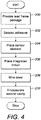
Figure 4 , thesensor device 100 is constructed as follows. The premoulded lead frame 102 (Figures 5, 6 and 7 ) is taken in an unpopulated state (Step 200), thefirst cavity 112 having thefirst base 108, which is empty, and thesecond cavity 114 having thesecond base 110, which is also empty. Thepartition wall 116 has the cut-out 118, which is also clear for receiving thepressure sensor element 120. - Turning to
Figures 8 and 9 , an adhesive 119 is applied (Step 202) to the site where thepressure sensor element 120 is to be deposited, for example in the cut-out 118, and the site where thedriver IC 138 is to be deposited. Thepressure sensor element 120 is then positioned (Step 204) in contact with the adhesive 119 in thelead frame package 102 so that the majority of thepressure sensor element 120 is suspended in thefirst cavity 112 and the remainder of thepressure sensor element 120 overlies the cut-out 118 in thepartition wall 116 and sufficiently into thesecond cavity 114 so that thefirst bond pads 128 are in thesecond cavity 114. Thedriver IC 138 is also positioned (Step 206) in contact with the adhesive 119 in thesecond cavity 114. Thefirst bond pads 128 of thepressure sensor element 120, thesecond bond pads 140 of thedriver IC 138 and the innerlead contact terminals bond wires pressure sensor element 120, thedriver IC 138 and the lead frame need to be interconnected to satisfy the circuit design of thesensor device 100. This is optional depending upon whether anything is disposed in thesecond cavity 114 to which connection is required. Thereafter, and referring toFigure 11 , theencapsulant material 150 is deposited (Step 210) in thesecond cavity 114, constituting a glob top, so as to encapsulate thesecond end 124 of thepressure sensor element 120, thedriver IC 138 and thewire bonding encapsulant material 150 into thefirst cavity 112 via the cut-out 118 in thepartition wall 116. - There completed
pressure sensor device 100 can then be used for various applications, for example in relation to vehicular applications, such as automotive applications. The completedpressure sensor device 100 can be brought into contact with and sealingly fixed to, for example, an access port to provide fluid communication between thesensor device 100 and a fluid the pressure of which is to be measured. The access port can be provided in any fluid system where fluid pressure is to be measured. In this regard, by virtue of thepressure sensor element 120 in thefirst cavity 112 being exposed, thepressure sensor element 120 is in fluid communication with fluid to be measured. - The skilled person should appreciate that the above-described implementations are merely examples of the various implementations that are conceivable within the scope of the appended claims. Indeed, it should be appreciated that in the examples described above, the volume of the first die-receiving subframe is closed at one end to form the
first cavity 110. However, in other embodiment, thefirst base 108 can be absent or thefirst base 108 can comprise an aperture so that the volume of the first die-receivingsubframe 104 is accessible from both sides of thelead frame package 102. In this regard, it can be seen that upper and lower surfaces of the pressure sensor element are, irrespective of orientation, exposed to ambient. It should also be appreciated that the apertures are not formed in upper and lower layers of surface material, but are instead simply openings in thelead frame package 102, i.e. the apertures can have substantially the same surface area as the footprint of thefirst cavity 112. - In another embodiment, the
pressure sensor device 100 can be formed so that thepressure sensor element 120 can be arranged to reside substantially in thefirst cavity 110 and extend into thepartition wall 116. In this respect, thesecond end 124 of thepressure sensor element 120 extends into the cut-out 118 in thepartition wall 116, but does not impinge on thesecond cavity 112. Any device disposed in thesecond cavity 112 can be electrically connected to thebond pads 128 at thesecond end 124 of thepressure sensor element 120, which would reside in the cut-out 118 of thepartition wall 116, prior to encapsulation. In this regard, the cut-out 118 into which thesecond end 124 of thepressure sensor element 120 extends is filled with, for example, a high-viscosity material that impedes progress of the encapsulant from thesecond cavity 124 into thefirst cavity 110. The encapsulant can then be, for example, "snap cured" using light, such as ultra-violet light, or heat, in order to prevent overflow of the encapsulant.
Claims (15)
- A method of manufacturing a sensor device, the method comprising:providing a package having a first die-receiving subframe volume separated from a second die-receiving subframe volume by a partition wall;disposing an elongate sensor element within the package so as to extend from the first subframe volume into the partition wall, the elongate sensor element residing substantially in the first subframe volume; andfilling the second subframe volume with an encapsulant material.
- A method as claimed in Claim 1, further comprising:disposing the elongate sensor element so as to bridge the first and second subframe volumes, thereby extending through the partition wall so as to reside partially in the second subframe volume.
- A method as claimed in Claim 1, further comprising:providing a sensing region at a first end of the elongate sensor element and an electrical contact at a second end of the elongate sensor element.
- A method as claimed in Claim 1 or Claim 2 or Claim 3, further comprising:disposing a circuit in the second subframe volume.
- A method as claimed in Claim 4, further comprising:electrically coupling the circuit to the elongate sensor element.
- A method as claimed in Claim 4 or Claim 5, further comprising:wire bonding with respect to the circuit and the elongate sensor element.
- A method as claimed in Claim 4 or Claim 5 or Claim 6, wherein the package comprises an internal lead contact terminal, and the circuit is a driver integrated circuit; and the method further comprises:wire bonding the driver integrated circuit to the elongate sensor element and to the internal lead contact terminal of the package.
- A method as claimed in any one of the preceding claims, further comprising:electrically connecting the elongate sensor element within the second subframe volume.
- A method as claimed in Claim 2, wherein the second end of the elongate sensor element protrudes into the second subframe volume; and the method further comprises:enveloping the second end of the elongate sensor element with the encapsulant material.
- A method as claimed in any one of the preceding claims, further comprising:providing the first and second subframe volumes as first and second cavities, respectively.
- A method as claimed in Claim 10, further comprising:providing the first and second cavities in stepped relation with respect to each other.
- A method as claimed in Claim 10 or Claim 11, further comprising:forming the first and second cavities so that the first cavity is deeper than the second cavity.
- A method as claimed in any one of Claims 1 to 9, wherein the elongate sensor element comprises an upper surface and a lower surface; and the method further comprises:providing the second subframe volume as a cavity; andconfiguring the first subframe volume so that the upper and lower surfaces of the elongate sensor element are exposed to ambient.
- A method as claimed in any one of the preceding claims, further comprising:forming the elongate sensor element as a pressure sensor.
- A sensor device comprising:a package having a first die-receiving subframe volume separated from a second die-receiving subframe volume by a partition wall;an elongate sensor element disposed within the package so as to extend from the first subframe volume into the partition wall, the elongate sensor element residing substantially in the first subframe volume; whereinthe elongate sensor element is enveloped with an encapsulant material.
Priority Applications (3)
| Application Number | Priority Date | Filing Date | Title |
|---|---|---|---|
| EP18192054.7A EP3618101A1 (en) | 2018-08-31 | 2018-08-31 | Sensor device and manufacturing method thereof |
| US16/557,224 US11600559B2 (en) | 2018-08-31 | 2019-08-30 | Sensor device and method of manufacture |
| CN201910813604.0A CN110875197A (en) | 2018-08-31 | 2019-08-30 | Sensor device and manufacturing method |
Applications Claiming Priority (1)
| Application Number | Priority Date | Filing Date | Title |
|---|---|---|---|
| EP18192054.7A EP3618101A1 (en) | 2018-08-31 | 2018-08-31 | Sensor device and manufacturing method thereof |
Publications (1)
| Publication Number | Publication Date |
|---|---|
| EP3618101A1 true EP3618101A1 (en) | 2020-03-04 |
Family
ID=63452575
Family Applications (1)
| Application Number | Title | Priority Date | Filing Date |
|---|---|---|---|
| EP18192054.7A Pending EP3618101A1 (en) | 2018-08-31 | 2018-08-31 | Sensor device and manufacturing method thereof |
Country Status (3)
| Country | Link |
|---|---|
| US (1) | US11600559B2 (en) |
| EP (1) | EP3618101A1 (en) |
| CN (1) | CN110875197A (en) |
Cited By (2)
| Publication number | Priority date | Publication date | Assignee | Title |
|---|---|---|---|---|
| WO2025098618A1 (en) * | 2023-11-09 | 2025-05-15 | Melexis Technologies Nv | Method of manufacturing a chemical sensor die |
| WO2025098619A1 (en) * | 2023-11-09 | 2025-05-15 | Melexis Technologies Nv | Sensing die and method of manufacture thereof |
Families Citing this family (2)
| Publication number | Priority date | Publication date | Assignee | Title |
|---|---|---|---|---|
| NL2020901B1 (en) * | 2018-05-09 | 2019-11-18 | Sencio B V | A sensor package and a method of manufacturing a sensor package |
| EP4390355B1 (en) * | 2022-12-23 | 2026-04-08 | Melexis Technologies NV | Protection of sensing element during moulding |
Citations (5)
| Publication number | Priority date | Publication date | Assignee | Title |
|---|---|---|---|---|
| US20050284216A1 (en) * | 2004-06-24 | 2005-12-29 | Denso Corporation | Sensor equipment having sensing portion and method for manufacturing the same |
| US20090102033A1 (en) | 2007-10-18 | 2009-04-23 | Elmos Advanced Packaging B.V. | Integrated circuit package |
| US20110296904A1 (en) * | 2010-06-02 | 2011-12-08 | Denso Corporation | Air flow rate measuring device |
| US20140360262A1 (en) * | 2012-01-10 | 2014-12-11 | Hitachi Automotive Systems, Ltd. | Flow Rate Measuring Device |
| US20170089796A1 (en) * | 2013-02-21 | 2017-03-30 | Epcos Ag | Pressure Sensor System |
Family Cites Families (6)
| Publication number | Priority date | Publication date | Assignee | Title |
|---|---|---|---|---|
| EP0363005B1 (en) * | 1988-09-02 | 1996-06-05 | Honda Giken Kogyo Kabushiki Kaisha | A semiconductor sensor |
| US20040189292A1 (en) * | 2003-03-25 | 2004-09-30 | Kautz David R. | Mechanism for and method of biasing magnetic sensor |
| JP4978587B2 (en) * | 2008-08-21 | 2012-07-18 | 株式会社デンソー | Sensor device and manufacturing method thereof |
| WO2012049742A1 (en) * | 2010-10-13 | 2012-04-19 | 日立オートモティブシステムズ株式会社 | Flow sensor and production method therefor, and flow sensor module and production method therefor |
| JP2013050458A (en) * | 2012-10-18 | 2013-03-14 | Hitachi Automotive Systems Ltd | Flow sensor, method of manufacturing the same, and flow sensor module |
| DE102014010116B4 (en) * | 2013-04-29 | 2018-11-15 | Elmos Semiconductor Aktiengesellschaft | MEMS sensor for difficult environments and media |
-
2018
- 2018-08-31 EP EP18192054.7A patent/EP3618101A1/en active Pending
-
2019
- 2019-08-30 CN CN201910813604.0A patent/CN110875197A/en active Pending
- 2019-08-30 US US16/557,224 patent/US11600559B2/en active Active
Patent Citations (5)
| Publication number | Priority date | Publication date | Assignee | Title |
|---|---|---|---|---|
| US20050284216A1 (en) * | 2004-06-24 | 2005-12-29 | Denso Corporation | Sensor equipment having sensing portion and method for manufacturing the same |
| US20090102033A1 (en) | 2007-10-18 | 2009-04-23 | Elmos Advanced Packaging B.V. | Integrated circuit package |
| US20110296904A1 (en) * | 2010-06-02 | 2011-12-08 | Denso Corporation | Air flow rate measuring device |
| US20140360262A1 (en) * | 2012-01-10 | 2014-12-11 | Hitachi Automotive Systems, Ltd. | Flow Rate Measuring Device |
| US20170089796A1 (en) * | 2013-02-21 | 2017-03-30 | Epcos Ag | Pressure Sensor System |
Cited By (2)
| Publication number | Priority date | Publication date | Assignee | Title |
|---|---|---|---|---|
| WO2025098618A1 (en) * | 2023-11-09 | 2025-05-15 | Melexis Technologies Nv | Method of manufacturing a chemical sensor die |
| WO2025098619A1 (en) * | 2023-11-09 | 2025-05-15 | Melexis Technologies Nv | Sensing die and method of manufacture thereof |
Also Published As
| Publication number | Publication date |
|---|---|
| US11600559B2 (en) | 2023-03-07 |
| CN110875197A (en) | 2020-03-10 |
| US20200075466A1 (en) | 2020-03-05 |
Similar Documents
| Publication | Publication Date | Title |
|---|---|---|
| EP3032227B1 (en) | Flow sensor package | |
| US11600559B2 (en) | Sensor device and method of manufacture | |
| US7568390B2 (en) | Semiconductor acceleration sensor device and method for manufacturing the same | |
| US6432737B1 (en) | Method for forming a flip chip pressure sensor die package | |
| US7793550B2 (en) | Sensor device including two sensors embedded in a mold material | |
| US6441503B1 (en) | Bond wire pressure sensor die package | |
| CN104517914B (en) | With integrated sealed pressure sensor package | |
| EP2680304B1 (en) | Film-assist molded gel-fill cavity package with overflow reservoir | |
| US20110156176A1 (en) | Leadframe-Based Premolded Package Having Acoustic Air Channel for Micro-Electro-Mechanical System | |
| JP3620185B2 (en) | Semiconductor sensor device | |
| KR20110128293A (en) | Exposed Pad Rear Pressure Sensor Package | |
| EP1671091A1 (en) | Surface mount package and method for forming multi-chip microsensor device | |
| US6420201B1 (en) | Method for forming a bond wire pressure sensor die package | |
| US9890034B2 (en) | Cavity type pressure sensor device | |
| US8264074B2 (en) | Device for use as dual-sided sensor package | |
| CN111664966B (en) | Pressure sensors for stress decoupling on flexible substrates | |
| US12024418B2 (en) | Method of manufacturing a sensor device and moulding support structure | |
| CN107036740A (en) | A kind of microsensor encapsulating structure and its manufacture craft | |
| CN109830477B (en) | Integrated circuit package and its manufacturing method and injection molding jig | |
| JP4326609B2 (en) | Method for manufacturing a semiconductor device | |
| CN209471962U (en) | Integrated circuit package body and its injection molding jig | |
| CN216246985U (en) | Pressure sensor | |
| CN112499577A (en) | Packaging structure, preparation method thereof and electronic device | |
| GB2432457A (en) | Sensor arrangement and method for fabricating a sensor arrangement |
Legal Events
| Date | Code | Title | Description |
|---|---|---|---|
| PUAI | Public reference made under article 153(3) epc to a published international application that has entered the european phase |
Free format text: ORIGINAL CODE: 0009012 |
|
| STAA | Information on the status of an ep patent application or granted ep patent |
Free format text: STATUS: THE APPLICATION HAS BEEN PUBLISHED |
|
| AK | Designated contracting states |
Kind code of ref document: A1 Designated state(s): AL AT BE BG CH CY CZ DE DK EE ES FI FR GB GR HR HU IE IS IT LI LT LU LV MC MK MT NL NO PL PT RO RS SE SI SK SM TR |
|
| AX | Request for extension of the european patent |
Extension state: BA ME |
|
| STAA | Information on the status of an ep patent application or granted ep patent |
Free format text: STATUS: REQUEST FOR EXAMINATION WAS MADE |
|
| 17P | Request for examination filed |
Effective date: 20200903 |
|
| RBV | Designated contracting states (corrected) |
Designated state(s): AL AT BE BG CH CY CZ DE DK EE ES FI FR GB GR HR HU IE IS IT LI LT LU LV MC MK MT NL NO PL PT RO RS SE SI SK SM TR |