DE102014010116B4 - MEMS sensor for difficult environments and media - Google Patents

MEMS sensor for difficult environments and media Download PDF

Info

Publication number
DE102014010116B4
DE102014010116B4 DE102014010116.9A DE102014010116A DE102014010116B4 DE 102014010116 B4 DE102014010116 B4 DE 102014010116B4 DE 102014010116 A DE102014010116 A DE 102014010116A DE 102014010116 B4 DE102014010116 B4 DE 102014010116B4
Authority
DE
Germany
Prior art keywords
sensor
region
micromechanical
area
cell
Prior art date
Legal status (The legal status is an assumption and is not a legal conclusion. Google has not performed a legal analysis and makes no representation as to the accuracy of the status listed.)
Active
Application number
DE102014010116.9A
Other languages
German (de)
Other versions
DE102014010116A1 (en
Inventor
Bernd Burchard
Current Assignee (The listed assignees may be inaccurate. Google has not performed a legal analysis and makes no representation or warranty as to the accuracy of the list.)
Measurement Specialties Inc Hampton Us
Original Assignee
Elmos Semiconductor SE
Priority date (The priority date is an assumption and is not a legal conclusion. Google has not performed a legal analysis and makes no representation as to the accuracy of the date listed.)
Filing date
Publication date
Application filed by Elmos Semiconductor SE filed Critical Elmos Semiconductor SE
Priority to DE102014010116.9A priority Critical patent/DE102014010116B4/en
Publication of DE102014010116A1 publication Critical patent/DE102014010116A1/en
Application granted granted Critical
Publication of DE102014010116B4 publication Critical patent/DE102014010116B4/en
Active legal-status Critical Current
Anticipated expiration legal-status Critical

Links

Images

Classifications

    • GPHYSICS
    • G01MEASURING; TESTING
    • G01DMEASURING NOT SPECIALLY ADAPTED FOR A SPECIFIC VARIABLE; ARRANGEMENTS FOR MEASURING TWO OR MORE VARIABLES NOT COVERED IN A SINGLE OTHER SUBCLASS; TARIFF METERING APPARATUS; MEASURING OR TESTING NOT OTHERWISE PROVIDED FOR
    • G01D11/00Component parts of measuring arrangements not specially adapted for a specific variable
    • G01D11/24Housings ; Casings for instruments
    • G01D11/245Housings for sensors
    • BPERFORMING OPERATIONS; TRANSPORTING
    • B81MICROSTRUCTURAL TECHNOLOGY
    • B81BMICROSTRUCTURAL DEVICES OR SYSTEMS, e.g. MICROMECHANICAL DEVICES
    • B81B7/00Microstructural systems; Auxiliary parts of microstructural devices or systems
    • B81B7/0032Packages or encapsulation
    • B81B7/0077Other packages not provided for in groups B81B7/0035 - B81B7/0074
    • GPHYSICS
    • G01MEASURING; TESTING
    • G01LMEASURING FORCE, STRESS, TORQUE, WORK, MECHANICAL POWER, MECHANICAL EFFICIENCY, OR FLUID PRESSURE
    • G01L19/00Details of, or accessories for, apparatus for measuring steady or quasi-steady pressure of a fluent medium insofar as such details or accessories are not special to particular types of pressure gauges
    • G01L19/06Means for preventing overload or deleterious influence of the measured medium on the measuring device or vice versa
    • G01L19/0627Protection against aggressive medium in general
    • G01L19/0645Protection against aggressive medium in general using isolation membranes, specially adapted for protection
    • GPHYSICS
    • G01MEASURING; TESTING
    • G01LMEASURING FORCE, STRESS, TORQUE, WORK, MECHANICAL POWER, MECHANICAL EFFICIENCY, OR FLUID PRESSURE
    • G01L19/00Details of, or accessories for, apparatus for measuring steady or quasi-steady pressure of a fluent medium insofar as such details or accessories are not special to particular types of pressure gauges
    • G01L19/14Housings
    • G01L19/142Multiple part housings
    • GPHYSICS
    • G01MEASURING; TESTING
    • G01LMEASURING FORCE, STRESS, TORQUE, WORK, MECHANICAL POWER, MECHANICAL EFFICIENCY, OR FLUID PRESSURE
    • G01L19/00Details of, or accessories for, apparatus for measuring steady or quasi-steady pressure of a fluent medium insofar as such details or accessories are not special to particular types of pressure gauges
    • G01L19/04Means for compensating for effects of changes of temperature, i.e. other than electric compensation
    • HELECTRICITY
    • H10SEMICONDUCTOR DEVICES; ELECTRIC SOLID-STATE DEVICES NOT OTHERWISE PROVIDED FOR
    • H10WGENERIC PACKAGES, INTERCONNECTIONS, CONNECTORS OR OTHER CONSTRUCTIONAL DETAILS OF DEVICES COVERED BY CLASS H10
    • H10W72/00Interconnections or connectors in packages
    • H10W72/071Connecting or disconnecting
    • H10W72/075Connecting or disconnecting of bond wires
    • H10W72/07541Controlling the environment, e.g. atmosphere composition or temperature
    • H10W72/07554Controlling the environment, e.g. atmosphere composition or temperature changes in dispositions
    • HELECTRICITY
    • H10SEMICONDUCTOR DEVICES; ELECTRIC SOLID-STATE DEVICES NOT OTHERWISE PROVIDED FOR
    • H10WGENERIC PACKAGES, INTERCONNECTIONS, CONNECTORS OR OTHER CONSTRUCTIONAL DETAILS OF DEVICES COVERED BY CLASS H10
    • H10W72/00Interconnections or connectors in packages
    • H10W72/50Bond wires
    • H10W72/531Shapes of wire connectors
    • H10W72/536Shapes of wire connectors the connected ends being ball-shaped
    • HELECTRICITY
    • H10SEMICONDUCTOR DEVICES; ELECTRIC SOLID-STATE DEVICES NOT OTHERWISE PROVIDED FOR
    • H10WGENERIC PACKAGES, INTERCONNECTIONS, CONNECTORS OR OTHER CONSTRUCTIONAL DETAILS OF DEVICES COVERED BY CLASS H10
    • H10W72/00Interconnections or connectors in packages
    • H10W72/50Bond wires
    • H10W72/531Shapes of wire connectors
    • H10W72/5363Shapes of wire connectors the connected ends being wedge-shaped
    • HELECTRICITY
    • H10SEMICONDUCTOR DEVICES; ELECTRIC SOLID-STATE DEVICES NOT OTHERWISE PROVIDED FOR
    • H10WGENERIC PACKAGES, INTERCONNECTIONS, CONNECTORS OR OTHER CONSTRUCTIONAL DETAILS OF DEVICES COVERED BY CLASS H10
    • H10W72/00Interconnections or connectors in packages
    • H10W72/50Bond wires
    • H10W72/541Dispositions of bond wires
    • H10W72/5445Dispositions of bond wires being orthogonal to a side surface of the chip, e.g. parallel arrangements
    • HELECTRICITY
    • H10SEMICONDUCTOR DEVICES; ELECTRIC SOLID-STATE DEVICES NOT OTHERWISE PROVIDED FOR
    • H10WGENERIC PACKAGES, INTERCONNECTIONS, CONNECTORS OR OTHER CONSTRUCTIONAL DETAILS OF DEVICES COVERED BY CLASS H10
    • H10W72/00Interconnections or connectors in packages
    • H10W72/50Bond wires
    • H10W72/541Dispositions of bond wires
    • H10W72/547Dispositions of multiple bond wires
    • HELECTRICITY
    • H10SEMICONDUCTOR DEVICES; ELECTRIC SOLID-STATE DEVICES NOT OTHERWISE PROVIDED FOR
    • H10WGENERIC PACKAGES, INTERCONNECTIONS, CONNECTORS OR OTHER CONSTRUCTIONAL DETAILS OF DEVICES COVERED BY CLASS H10
    • H10W72/00Interconnections or connectors in packages
    • H10W72/851Dispositions of multiple connectors or interconnections
    • H10W72/874On different surfaces
    • H10W72/884Die-attach connectors and bond wires
    • HELECTRICITY
    • H10SEMICONDUCTOR DEVICES; ELECTRIC SOLID-STATE DEVICES NOT OTHERWISE PROVIDED FOR
    • H10WGENERIC PACKAGES, INTERCONNECTIONS, CONNECTORS OR OTHER CONSTRUCTIONAL DETAILS OF DEVICES COVERED BY CLASS H10
    • H10W72/00Interconnections or connectors in packages
    • H10W72/90Bond pads, in general
    • H10W72/931Shapes of bond pads
    • H10W72/932Plan-view shape, i.e. in top view
    • HELECTRICITY
    • H10SEMICONDUCTOR DEVICES; ELECTRIC SOLID-STATE DEVICES NOT OTHERWISE PROVIDED FOR
    • H10WGENERIC PACKAGES, INTERCONNECTIONS, CONNECTORS OR OTHER CONSTRUCTIONAL DETAILS OF DEVICES COVERED BY CLASS H10
    • H10W74/00Encapsulations, e.g. protective coatings
    • HELECTRICITY
    • H10SEMICONDUCTOR DEVICES; ELECTRIC SOLID-STATE DEVICES NOT OTHERWISE PROVIDED FOR
    • H10WGENERIC PACKAGES, INTERCONNECTIONS, CONNECTORS OR OTHER CONSTRUCTIONAL DETAILS OF DEVICES COVERED BY CLASS H10
    • H10W74/00Encapsulations, e.g. protective coatings
    • H10W74/10Encapsulations, e.g. protective coatings characterised by their shape or disposition
    • H10W74/111Encapsulations, e.g. protective coatings characterised by their shape or disposition the semiconductor body being completely enclosed
    • H10W74/114Encapsulations, e.g. protective coatings characterised by their shape or disposition the semiconductor body being completely enclosed by a substrate and the encapsulations
    • HELECTRICITY
    • H10SEMICONDUCTOR DEVICES; ELECTRIC SOLID-STATE DEVICES NOT OTHERWISE PROVIDED FOR
    • H10WGENERIC PACKAGES, INTERCONNECTIONS, CONNECTORS OR OTHER CONSTRUCTIONAL DETAILS OF DEVICES COVERED BY CLASS H10
    • H10W90/00Package configurations
    • H10W90/701Package configurations characterised by the relative positions of pads or connectors relative to package parts
    • H10W90/751Package configurations characterised by the relative positions of pads or connectors relative to package parts of bond wires
    • H10W90/753Package configurations characterised by the relative positions of pads or connectors relative to package parts of bond wires between laterally-adjacent chips

Landscapes

  • Engineering & Computer Science (AREA)
  • Microelectronics & Electronic Packaging (AREA)
  • Physics & Mathematics (AREA)
  • General Physics & Mathematics (AREA)
  • Computer Hardware Design (AREA)
  • Measuring Fluid Pressure (AREA)
  • Pressure Sensors (AREA)

Abstract

Mikromechanischer Sensor (3) aus Silizium und- mit mindestens einer Sensorzelle (8) und- und mindestens einem Funktionselement (7) dass dazu vorgesehen ist oder dazu verwendet werden kann, in direkten Kontakt mit einem Medium zu stehen,dadurch gekennzeichnet,- dass der mikromechanische Sensor (3) auf der CMOS-prozessierten Oberfläche zumindest einem ersten Bereich (A) aufweist und• dass dieser erste Bereich (A) zumindest eine Sensorzelle (8) mit einer vergrabenen Kavität (71) aufweist und• dass der erste Bereich (A) zumindest eine Sensormesszelle (8) umfasst und• dass der erste Bereich (A) für den direkten Kontakt mit einem Medium vorgesehen ist oder verwendet werden kann und• dass der erste Bereich (A)◯ keine Metallisierung aufweist und/ oder◯ in diesem ersten Bereich (A) elektrische Verbindungen in dotiertem Halbleitermaterial und/oder polykristallinem Halbleitermaterial ausgeführt sind und- dass der mikromechanische Sensor (3) auf seiner CMOS-prozessierten Oberfläche zumindest einen zweiten Bereich (B) aufweist und• dass es die Funktion des zweiten Bereiches (B) ist, zusammen mit einer ersten Dichtung (11) oder Moldmasse (77) den Durchtritt des Mediums in einen dritten Bereich (C) des mikromechanischen Sensors abzudichten und damit zu verhindern und• dass er in diesem zweiten Bereich (B)◯ keine Metallisierung aufweist und/ oder◯ in diesem zweiten Bereich (B) elektrische Verbindungen in dotiertem Halbleitermaterial oder polykristallinem Halbleitermaterial ausgeführt sind und- dass der mikromechanische Sensor (3) einen dritten Bereich (C) auf seiner CMOS-prozessierten Oberfläche aufweist und• dass der dritte Bereich (C) zumindest einen metallischen elektrischen Kontakt des mikromechanischen Sensors (3) aufweist und• dass der zweite Bereich (B) sich auf der prozessierten Oberfläche immer zwischen dem dritten Bereich (C) und dem ersten Bereich (A) befindet und• dass der dritte Bereich (C) von dem ersten Bereich (A)auf der prozessierten Oberfläche nicht berührt wird und- dass er ein Drucksensor ist oder zumindest eine Sensorzelle (8) aufweist, die eine Drucksensorzelle ist, und- dass er einen Temperatursensor (75) aufweist oder- eine Temperatursensorzelle aufweist.Micromechanical sensor (3) made of silicon and having at least one sensor cell (8) and at least one functional element (7) that is provided or can be used to be in direct contact with a medium, characterized in that - micromechanical sensor (3) on the CMOS-processed surface at least a first region (A) and • that this first region (A) has at least one sensor cell (8) with a buried cavity (71) and • that the first region (A ) comprises at least one sensor measuring cell (8) and • that the first region (A) is or can be used for direct contact with a medium and • that the first region (A) ◯ has no metallization and / or ◯ in the first Area (A) electrical connections in doped semiconductor material and / or polycrystalline semiconductor material are executed and that the micromechanical sensor (3) on its CMOS-processed surface e has at least a second region (B) and that it is the function of the second region (B) together with a first seal (11) or molding compound (77) the passage of the medium in a third region (C) of the micromechanical sensor seal and thus prevent and • that in this second region (B) ◯ has no metallization and / or ◯ in this second region (B) electrical connections in doped semiconductor material or polycrystalline semiconductor material are executed and that the micromechanical sensor (3) a third region (C) on its CMOS-processed surface, and • that the third region (C) has at least one metallic electrical contact of the micromechanical sensor (3) and that the second region (B) always lies on the processed surface the third region (C) and the first region (A) and • that the third region (C) of the first region (A) on the processed surface is not touched and that it is a pressure sensor or at least one sensor cell (8) which is a pressure sensor cell, and that it has a temperature sensor (75) or has a temperature sensor cell.

Description

Einleitungintroduction

In vielen Anwendungen ist die Messung von Drücken in schwierigen Umgebungen von besonderer Bedeutung. Hierbei ergibt sich das Problem, dass die Drucksensoren mit dem Mediendruck versorgt werden müssen. Hierfür sollen die Drucksensoren möglichst nahe an den Druckraum herangebracht werden, um Verfälschungen des Messergebnisses zu verhindern. Ein direkter Kontakt zwischen der Sensormembrane und dem zu vermessenden Medium ist wünschenswert.In many applications, the measurement of pressures in difficult environments is of particular importance. This results in the problem that the pressure sensors must be supplied with the media pressure. For this purpose, the pressure sensors should be brought as close as possible to the pressure chamber to prevent distortions of the measurement result. Direct contact between the sensor membrane and the medium to be measured is desirable.

Im Stand der Technik sind hierzu verschiedene Lösungen bekannt. Als Beispiel ist die US 8 049 290 B2 (US 2009/ 0 206 467 A1) zu nennen, bei der das Medium über die Rückseite eines Plastikgehäuses zugeführt wird. Der in der US 8 049 290 B2 ( US 2009/ 0 206 467 A1 ) dargestellte Sensor (Bezugszeichen 2 der US 8 049 290 B2 , US 2009/ 0 206 467 A1 ) besteht aus drei Teilen: Einem mittleren MEMS-Chip, der an seiner Oberseite, also der der Zutrittsöffnung gegenüberliegenden Sensoroberfläche die eigentlichen piezoresistiven Sensorstrukturen auf der CMOS prozessierten Oberfläche aufweist, einer darauf gebondeten Glaskappe, die mit dem mittleren Chip typischerweise die ebenso typischerweise evakuierte Referenz-Kavität bildet und einem unteren Chip, dem sogenannten Constraint-Wafer, mit einer Bohrung, die durch diesen unteren Chip und typischerweise bis in den mittleren Bereich hinein reicht. Ein solcher Sensor ist ohne Constraint-Wafer beispielsweise aus der US 2003/ 0 167 851 A1 bekannt. Der Sensor der US 2003/ 0 167 851 A1 wird aber in einem üblichen Verfahren typischerweise noch mit einer durchbohrten Bodenplatte aus Glas, dem besagten Constraint-Wafer, versehen, der das Flächenträgheitsmoment des mikromechanischen Drucksensors erhöht und damit dessen Verwindungssteifheit anhebt. Diese Glaskomponente ist in der US 8 049 290 B2 ( US 2009/ 0 206 467 A1 ) mit Zutrittsloch zusätzlich gegenüber der US 2003/ 0 167 851 A1 eingezeichnet. Das Sensorpaket (Bezugszeichen 2 der US 8 049 290 B2 , US 2009/ 0 206 467 A1 ) wird in der US 8 049 290 B2 ( US 2009/ 0 206 467 A1 ) auf einen Leadframe geklebt (Bezugszeichen 3 der US 8 049 290 B2 , US 2009/ 0 206 467 A1 ). Damit der Leadframe nicht korrodiert, bedeckt die Moldmasse (Bezugszeichen 5 der US 8 049 290 B2 , US 2009/ 0 206 467 A1 ) im Bereich der Zutrittsöffnung (Bezugszeichen 21 der US 8 049 290 B2 , US 2009/ 0 206 467 A1 ) auch den Leadframe (Bezugszeichen 3 der US8049290B2 , US 2009/ 0 206 467 A1 ). Der wesentliche Nachteil dieser sehr aufwendigen Technik ist, dass sie zum einen eine komplexe Glaskappe (Bezugszeichen 54 der US 2003/ 0 167 851 A1) und zum anderen einen sehr teuren Ätzschritt zum Durchätzen des Substrates (Bezugszeichen 38 der US 2003/ 0 167 851 A1 ) zur Ausformung der Membrane (Bezugszeichen 40 der US 2003/ 0 167 851 A1 ) erfordert. Der Druck kann in der Konstruktion der US 8 049 290 B2 ( US 2009/ 0 206 467 A1 ) von der Rückseite her die Membrane (Bezugszeichen 40 der US 2003/ 0 167 851 A1 ), nicht jedoch die auf der anderen Seite der Membrane, der CMOS-prozessierten Vorderseite, liegenden elektronischen Bauteile erreichen. Auf der CMOS-prozessierten Vorderseite liegen auch die Bonddrähte (Bezugszeichen 6 der US 8 049 290 B2 , US 2009/ 0 206 467 A1). Diese sind damit ebenso wie die Bond-Pads des Drucksensors (Bezugszeichen 2 der US 8 049 290 B2 , US 2009/ 0 206 467 A1 ) und des Auswerteschaltkreises (Bezugszeichen 10 der US 8 049 290 B2 , US 2009/ 0 206 467 A1 ) vor Korrosion durch das Medium, dessen Druck gemessen werden soll, geschützt. Ein Nachteil einer solchen Lösung zur Messung des Drucks in aggressiven Medien ist darüber hinaus, dass die Ausdehnung eines solchen Sensors so groß ist, dass er nicht in eine M5-Schraube integriert werden kann. Auch müssen auftretende mechanischer Spannungen zwischen einer Vergussmasse, dem Sensorelement und dem Sensorgehäuse so abgefangen werden, dass es zu keiner Veränderung des Messsignals kommt. Dies alles ist insbesondere bei der Integration in eine Schraube zur beispielhaften Verwendung in einer Ölwanne eines Kfz kritisch. Zu diesem Zweck ist es sinnvoll, ja nahezu erforderlich, wenn das jeweilige drucksensitive Element in eine Schraube eingebaut werden kann, die dann wiederum sehr leicht in einen Tank, ein Rohr oder dergleichen zur Messung des Druckes eines Mediums in dem Rohr eingebaut werden kann. Ein solches Sensorsystem ist beispielsweise aus der DE 30 21 088 A1 bekannt. Dieser Sensor, der den Druck während der Verbrennung im Zylinderraum misst, ist nur zur Messung hoher Drücke geeignet. Die Offenbarung DE 30 21 088 A1 lässt dabei vollkommen offen, wie die in der Offenbarung erwähnten Elektroden vor Korrosion geschützt werden. Für die Ko-Integration eines Verstärkers sind die vorgeschlagenen Materialien Kunststoff / Keramik vollkommen ungeeignet, da es sich nicht um ein Halbleitermaterial handelt.In the prior art, various solutions are known for this purpose. As an example, the US 8 049 290 B2 (US 2009/0 206 467 A1), in which the medium is supplied via the rear side of a plastic housing. The Indian US 8 049 290 B2 ( US 2009/0 206 467 A1 ) shown sensor (reference 2 of the US 8 049 290 B2 . US 2009/0 206 467 A1 ) consists of three parts: A middle MEMS chip, which has the actual piezoresistive sensor structures on the CMOS processed surface on its upper side, ie the sensor surface opposite the access opening, a glass cap bonded thereto, which typically also has the typically evacuated reference with the middle chip -Cavity forms and a lower chip, the so-called constraint wafer, with a hole that extends through this lower chip and typically into the middle region. Such a sensor is without Constraint Wafer example from the US 2003/0 167 851 A1 known. However, the sensor of US 2003/0 167 851 A1 is typically provided in a conventional method with a pierced bottom plate made of glass, said constraint wafer, which increases the area moment of inertia of the micromechanical pressure sensor and thus increases its torsional stiffness. This glass component is in the US 8 049 290 B2 ( US 2009/0 206 467 A1 ) with access hole in addition to the US 2003/0 167 851 A1 located. The sensor package (reference 2 of the US 8 049 290 B2 . US 2009/0 206 467 A1 ) is in the US 8 049 290 B2 ( US 2009/0 206 467 A1 ) glued on a leadframe (reference numeral 3 of US 8 049 290 B2 . US 2009/0 206 467 A1 ). So that the leadframe does not corrode, the molding compound (reference numeral 5 of FIG US 8 049 290 B2 . US 2009/0 206 467 A1 ) in the region of the access opening (reference numeral 21 of the US 8 049 290 B2 . US 2009/0 206 467 A1 ) also the leadframe (reference 3 of the US8049290B2 . US 2009/0 206 467 A1 ). The main drawback of this very expensive technique is that on the one hand a complex glass cap (reference number 54 of US 2003/0 167 851 A1) and on the other hand a very expensive etching step for etching through the substrate (reference numeral 38 of FIG US 2003/0 167 851 A1 ) for forming the membrane (reference numeral 40 of US 2003/0 167 851 A1 ) requires. The pressure may be in the construction of the US 8 049 290 B2 ( US 2009/0 206 467 A1 ) from the back the membrane (reference numeral 40 of US 2003/0 167 851 A1 ), but not the electronic components located on the other side of the diaphragm, the CMOS-processed front. On the CMOS-processed front are also the bonding wires (reference 6 of the US 8 049 290 B2 , US 2009/0 206 467 A1). These are thus as well as the bond pads of the pressure sensor (reference 2 of the US 8 049 290 B2 . US 2009/0 206 467 A1 ) and the evaluation circuit (reference numeral 10 of US 8 049 290 B2 . US 2009/0 206 467 A1 ) protected against corrosion by the medium whose pressure is to be measured. A disadvantage of such a solution for measuring the pressure in aggressive media, moreover, is that the extent of such a sensor is so large that it can not be integrated into an M5 screw. Also occurring mechanical stresses between a potting compound, the sensor element and the sensor housing must be intercepted so that there is no change in the measurement signal. All this is particularly critical in integration into a screw for exemplary use in an oil pan of a motor vehicle. For this purpose, it is useful, almost necessary if the respective pressure-sensitive element can be installed in a screw, which in turn can be very easily installed in a tank, a pipe or the like for measuring the pressure of a medium in the pipe. Such a sensor system is for example from the DE 30 21 088 A1 known. This sensor, which measures the pressure during combustion in the cylinder chamber, is only suitable for measuring high pressures. The revelation DE 30 21 088 A1 leaves completely open as to how the electrodes mentioned in the disclosure are protected from corrosion. For the co-integration of an amplifier, the proposed materials plastic / ceramic are completely unsuitable because it is not a semiconductor material.

Auch aus der DE 10 360 941 A1 ist eine Schraube als äußere Form eines Sensorsystems bekannt. Das Problem der Korrosion der Leitungen und ggf. auch der Sensorelemente wird in dieser Offenbarung so gelöst, dass das eine Messeinrichtung (Bezugszeichen 6 der DE 10 360 941 A1 ) auf einer Membrane, oder „Materialschwächung“ (Bezugszeichen 23 der DE 10 360 941 A1 ) angebracht wird. Dabei wurde diese Membrane (Bezugszeichen 23 der DE 10 360 941 A1 ) zusammen mit dem Grundkörper (Bezugszeichen 2 der DE 10 360 941 A1 ), also dem Schraubenkörper, gefertigt. Diese an sich schon sehr gute Lösung führt allerdings dazu, dass die Messvorrichtung (Bezugszeichen 6 der DE 10 360 941 A1 ) eben nicht mehr in direktem Kontakt mit dem zu vermessenden Medium ist, sondern der Druck im Medium erst durch die Materialschwächung und das Befestigungsmittel der Messeinrichtung übertragen werden muss. Diese Konstruktion ist für MEMS-Systeme ungeeignet.Also from the DE 10 360 941 A1 For example, a screw is known as the outer shape of a sensor system. The problem of corrosion of the lines and possibly also of the sensor elements is solved in this disclosure so that the one measuring device (reference numeral 6 of the DE 10 360 941 A1 ) on a membrane, or "material weakening" (reference numeral 23 of FIG DE 10 360 941 A1 ) is attached. In this case, this membrane (reference 23 of the DE 10 360 941 A1 ) together with the main body (reference 2 of the DE 10 360 941 A1 ), ie the screw body. This in itself very much However, good solution leads to the fact that the measuring device (reference numeral 6 of the DE 10 360 941 A1 ) is no longer in direct contact with the medium to be measured, but the pressure in the medium must be transmitted only by the material weakening and the fastening means of the measuring device. This design is unsuitable for MEMS systems.

In der Offenbarung DE 10 2004 002 089 A1 wird ein Drucksensorsystem in Form einer Schraube offenbart, das ebenfalls der Messung des Innendruckes in den Zylindern einer Verbrennungskraftmaschine dienen soll. Das Sensorelement (Bezugszeichen 21 der DE 10 2004 002 089 A1 ) ist dabei nicht näher spezifiziert. In der DE 10 2004 002 089 A1 wird nicht näher erläutert, wie das Leitungssystem des Sensorsystems (Bezugszeichen 21 der DE 10 2004 002 089 A1 ) gegen Korrosion in dieser extremen Umgebung geschützt wird. Darüber hinaus ist das Sensorelement (Bezugszeichen 21 der DE 10 2004 002 089 A1 ) mit der Flächennormale parallel zu der Achse des Sensorsystems montiert, was eine Vergrößerung der Bohrung zur Folge hat, da die Leitungen typischerweise von den Seiten her zugeführt werden müssen. Daher ist die Schraube und der Schraubenkopf in der DE 10 2004 002 089 A1 auch folgerichtig größer als der Schaft eingezeichnet. Diese vergrößerte Bohrung führt zu einer Schwächung des Druckraumes.In the Revelation DE 10 2004 002 089 A1 discloses a pressure sensor system in the form of a screw, which is also intended to measure the internal pressure in the cylinders of an internal combustion engine. The sensor element (reference numeral 21 of the DE 10 2004 002 089 A1 ) is not specified. In the DE 10 2004 002 089 A1 is not explained in detail how the line system of the sensor system (reference numeral 21 of DE 10 2004 002 089 A1 ) is protected against corrosion in this extreme environment. In addition, the sensor element (reference numeral 21 of the DE 10 2004 002 089 A1 ) is mounted with the surface normal parallel to the axis of the sensor system, resulting in an enlargement of the bore, as the lines typically have to be fed from the sides. Therefore, the screw and the screw head in the DE 10 2004 002 089 A1 logically larger than the shaft drawn. This enlarged bore leads to a weakening of the pressure chamber.

Auch aus der DE 10 2008 046 515 A1 und der DE 10 2009 048 702 A1 sind ähnliche Schraubenlösungen bekannt, die jedoch den direkten Kontakt eines mikromechanischen Drucksensors mit einem aggressiven Medium ebenfalls nicht zulassen.Also from the DE 10 2008 046 515 A1 and the DE 10 2009 048 702 A1 Similar screw solutions are known which, however, also do not allow the direct contact of a micromechanical pressure sensor with an aggressive medium.

Insbesondere für die Messung aggressiver Flüssigkeiten, wie beispielsweise Motorenöl erfreuen sich zunehmend jedoch mikromechanische Drucksensoren steigender Beliebtheit, da sie kostengünstig in großen Mengen herstellbar sind und eine ganze Reihe weiterer aus dem Stand der Technik bekannte Vorteile aufweisen. Hierfür müssen die typischerweise aus Silizium gefertigten mikromechanischen Drucksensoren in einer geeigneten Messvorrichtung mit dem zu erfassenden Druck des zu vermessenden Mediums in möglichst direkten Kontakt gebracht werden. Wird eine Wheatstone-Brücke implementiert, so ist es Stand der Technik, die Zuleitungen möglichst niederohmig in Metall auszuführen. Es ist außerdem eine allgemein verbreitete Auffassung, dass das jeweilige Medium, insbesondere Motorenöle und andere Kfz-Betriebsstoffe im Laufe der Lebensdauer des jeweiligen Produkts eine mehr oder weniger undefinierte Zusammensetzung annehmen. Daher herrscht unter den Fachleuten derzeit die weit verbreitete Annahme, dass die elektrischen Strukturen der Drucksensoren, die typischerweise in CMOS-Technik oder einer ähnlichen Halbleitertechnologie hergestellt sind, im Stand der Technik räumlich möglichst weit von dem typischerweise aggressiven Medium getrennt werden sollten. Insbesondere sollte das Medium nicht in direkten Kontakt mit der CMOS-prozessierten Oberseite des jeweiligen MEMS -Drucksensors, also typischerweise den CMOS Komponenten, kommen. Ursache hierfür sind kleine CMOS-Prozessierungsfehler, sogenannte Pin-Holes, die zu Löchern in dem Passivierungsschutz führen und daher den Zutritt des aggressiven Mediums zu durch diese ätzbaren Strukturen erlauben. Solche Pin-Holes sind darüber hinaus nicht elektrisch im Band-Ende-Test der Halbleiterherstellung testbar und damit sehr kritisch. Dieses Paradigma führt zu den bekannten verschiedenen Nachteilen. Insbesondere im Falle einer gleichzeitigen Temperaturmessung führt dies zu Problemen mit der Reaktionsgeschwindigkeit des Systems, da die Wärmekapazität ganz erheblich erhöht wird und der Temperatursensor in der Regel weiter vom Medium platziert werden muss.However, especially for the measurement of aggressive liquids, such as engine oil, micromechanical pressure sensors are becoming increasingly popular because they can be produced inexpensively in large quantities and have a whole series of further advantages known from the prior art. For this purpose, the micromechanical pressure sensors, which are typically made of silicon, must be brought into the most direct possible contact with the pressure of the medium to be measured in a suitable measuring device. If a Wheatstone bridge implemented, it is state of the art to perform the leads as low as possible in metal. It is also a common belief that the particular medium, in particular engine oils and other automotive consumables, assume a more or less undefined composition throughout the life of the particular product. Therefore, there is currently a widespread belief among those skilled in the art that the electrical structures of the pressure sensors, typically made in CMOS or similar semiconductor technology, should be spatially separated as far as possible from the typically aggressive medium in the art. In particular, the medium should not come into direct contact with the CMOS-processed upper side of the respective MEMS pressure sensor, ie typically the CMOS components. This is due to small CMOS processing errors, so-called pin-holes, which lead to holes in the passivation protection and therefore allow the access of the aggressive medium through these etchable structures. In addition, such pin-holes are not electrically testable in the band-end test of semiconductor production and are thus very critical. This paradigm leads to the known various disadvantages. In particular, in the case of a simultaneous temperature measurement, this leads to problems with the reaction rate of the system, since the heat capacity is increased significantly and the temperature sensor usually has to be placed further from the medium.

Allen bis hierhin beschriebenen Lösungen, bis auf einer, ist gemeinsam, dass sie das Problem des Schutzes eines mikromechanischen Drucksensors nur unvollständig lösen.All but one of the solutions described so far has one thing in common: they only incompletely solve the problem of protecting a micromechanical pressure sensor.

Einzig das in der US 8 049 290 B2 ( US 2009/ 0 206 467 A1 ) benannte Gehäuse löst dieses Problem, wenn es in eine Schraube eingebaut wird. Der dort verwendete mikromechanische Sensor ist aber relativ komplex und damit teuer.Only in the US 8 049 290 B2 ( US 2009/0 206 467 A1 ) named housing solves this problem when it is installed in a screw. However, the micromechanical sensor used there is relatively complex and therefore expensive.

Die WO 2011/ 083 161 A2 zeigt eine Oberflächenmikromechanik-Technologie und zugehörige Drucksensoren, ohne jedoch die konstruktiven Merkmale zu benennen, die erforderlich sind, um einen zuverlässigen Korrosionsschutz für die Metallisierung sicherzustellen. Die WO 2011/ 083 161 A2 zeigt verschiedene Möglichkeiten Drucksensoren mit Hilfe von Transistoren zu realisieren. Hierbei können die Gates als elektrostatische Schilde wirken, die die Eindiffusion von Protonen in die piezoresistiven Widerstände, die Transistoren, verhindern.The WO 2011/083 161 A2 shows surface micromechanical technology and associated pressure sensors without, however, naming the design features required to ensure reliable corrosion protection for the metallization. The WO 2011/083 161 A2 shows different ways to realize pressure sensors with the help of transistors. Here, the gates can act as electrostatic shields, which prevent the diffusion of protons into the piezoresistive resistors, the transistors.

Aus der DE 10 2004 027 094 A1 ist ebenfalls ein geeignetes Gehäuse bekannt, das durch Laser-Bearbeitung hergestellt wird. Der Korrosionsschutz soll durch ein optionales Gel (Abschnitt [0012] der DE 10 2004 027 094 A1 ) hergestellt werden. Darüber hinaus wird aber völlig offengelassen, wie der Sensor und insbesondere die Verbindungen zwischen Bondsystem und Sensorzelle beschaffen sein muss, um an seiner CMOS-prozessierten Oberfläche nicht korrodiert zu werden.From the DE 10 2004 027 094 A1 Also, a suitable housing is known, which is produced by laser machining. The corrosion protection should be ensured by an optional gel (section [0012] of DE 10 2004 027 094 A1 ) getting produced. In addition, however, it is left completely open as to how the sensor and in particular the connections between the bonding system and the sensor cell must be designed in order not to be corroded on its CMOS-processed surface.

Auch die DE 10 2008 011 943 A1 offenbart eine Sensoranordnung mit einem Drucksensor, der mit einem Ende freischwebend im Medium platziert wird. Hierbei reicht allerdings der Lead-Frame (Bezugszeichen 25 der DE 10 2008 011 943 A1 ) des Konstruktes bis in den Messraum (Bezugszeichen 31 der DE 10 2008 011 943 A1 ) hinein und ist damit der Korrosion ausgesetzt. Darüber hinaus wird auch hier völlig offengelassen, wie der Sensor und insbesondere die Verbindungen zwischen Bondsystem und Sensorzelle beschaffen sein muss, um an seiner CMOS-prozessierten Oberfläche nicht korrodiert zu werden. Einzig die Moldmasse wird als Schutz in Abschnitt [0017] der DE 10 2008 011 943 A1 erwähnt. Hierbei gilt es aber zu beachten, dass es zu einem Kapillareffekt zwischen Moldmasse und SensorChip kommen kann. Das Medium kann also, insbesondere, wenn der Sensor im Betrieb Temperaturwechseln ausgesetzt ist, zwischen Sensorchip und Moldmasse ein gewisses Stück eindringen.Also the DE 10 2008 011 943 A1 discloses a sensor assembly with a pressure sensor placed in free float with one end in the medium. Here, however, the lead frame (reference numeral 25 of the DE 10 2008 011 943 A1 ) of Constructs into the measuring room (reference 31 of the DE 10 2008 011 943 A1 ) and is thus exposed to corrosion. In addition, it is also left completely open here how the sensor, and in particular the connections between the bonding system and the sensor cell, must be designed in order not to be corroded on its CMOS-processed surface. Only the molding compound is used as protection in section [0017] of DE 10 2008 011 943 A1 mentioned. However, it should be noted that there may be a capillary effect between molding compound and sensor chip. Thus, in particular, when the sensor is exposed to temperature changes during operation, the medium can penetrate a certain distance between the sensor chip and the molding compound.

Die DE 10 2010 043 982 A1 offenbart hier eine weiterführende Sensoranordnung. Zum einen offenbart sie, dass die Zuleitungen in der Passivierung eingebettet und mit einer Passivierung bedeckt sein sollten (Abschnitt [0024] der DE 10 2010 043 982 A1 ). Zum anderen offenbart sie, wie die vorhergehenden Schriften, dass die Moldmasse (Bezugszeichen 20 der DE 10 2010 043 982 A1 ) die Abschnitte des Trägers (Bezugszeichen 15 der DE 10 2010 043 982 A1 ) schützt (Abschnitt [0027] der DE 10 2010 043 982 A1 ). Hierbei reicht allerdings auch hier der Lead-Frame (Bezugszeichen 15 der DE 10 2010 043 982 A1 ) des Konstrukts bis in den Messraum (Bezugszeichen 21 der DE 10 2010 043 982 A1 ) hinein und ist damit der Korrosion ausgesetzt. Darüber hinaus wird auch hier völlig offengelassen, wie der Sensor und insbesondere die Verbindungen zwischen Bondsystem und Sensorzelle beschaffen sein muss, um an seiner CMOS-prozessierten Oberfläche nicht korrodiert zu werden. Dies gilt auch für den Auswerteschaltkreis (Bezugszeichen 44 der DE 10 2010 043 982 A1 ). Darüber hinaus offenbart die DE 10 2010 043 982 A1 eine Stressentkopplungsstruktur (Bezugszeichen 13 der DE 10 2010 043 982 A1 ) zwischen Sensorbereich (Bezugszeichen 11 der DE 10 2010 043 982 A1 ) und Moldmassenkörper, die durch geeignete Gräben etc. (Bezugszeichen 81 und 82 der DE 10 2010 043 982 A1 ) gekennzeichnet ist.The DE 10 2010 043 982 A1 discloses here a further sensor arrangement. On the one hand, it discloses that the leads should be embedded in the passivation and covered with a passivation (section [0024] FIG DE 10 2010 043 982 A1 ). On the other hand, like the preceding documents, it discloses that the molding compound (reference 20 of the DE 10 2010 043 982 A1 ) the portions of the carrier (reference numeral 15 of DE 10 2010 043 982 A1 ) protects (section [0027] the DE 10 2010 043 982 A1 ). Here, however, the lead frame (reference numeral 15 of the DE 10 2010 043 982 A1 ) of the construct into the measuring space (reference 21 of the DE 10 2010 043 982 A1 ) and is thus exposed to corrosion. In addition, it is also left completely open here how the sensor, and in particular the connections between the bonding system and the sensor cell, must be designed in order not to be corroded on its CMOS-processed surface. This also applies to the evaluation circuit (reference numeral 44 of DE 10 2010 043 982 A1 ). In addition, the reveals DE 10 2010 043 982 A1 a stress decoupling structure (reference 13 of the DE 10 2010 043 982 A1 ) between sensor area (reference numeral 11 of FIG DE 10 2010 043 982 A1 ) and Moldmassenkörper which by suitable trenches, etc. (reference numerals 81 and 82 of DE 10 2010 043 982 A1 ).

Beispielsweise aus der US 2005 / 0 121 734 A1 ist bekannt, dass die elektrischen Verbindungen aus dotiertem Silizium des Substrates, dotierten Poly-Silizium, leitfähigem Metall oder anderen leitfähigen Materialien bestehen können (Abschnitt [0031] der US 2005 / 0 121 734 A1 ). Hierbei werden auch die Metalle Aluminium, Gold, Chrom erwähnt (Abschnitte [0040] und [0044] der US 2005 / 0 121 734 A1 ). Der Korrosionsschutz soll durch einen Silizium-Nitrid-Layer (Abschnitt [0041] der US 2005 / 0 121 734 A1 ) gewährleistet werden, der aber aufgrund der Pin-Hole-Problematik für den Einsatz in aggressiven Umgebungen nicht geeignet ist. Wie die Struktur der Verdrahtung gestaltet werden muss, um eine Korrosion, insbesondere des Bond-Systems, im Zusammenspiel mit einem Gehäuse zu verhindern, wird dabei nicht offenbart oder erkannt.It is known from US 2005/0 121 734 A1, for example, that the electrical connections can consist of doped silicon of the substrate, doped poly-silicon, conductive metal or other conductive materials (Section [0031] FIG US 2005/0 121 734 A1 ). Here, the metals aluminum, gold, chromium are mentioned (sections [0040] and [0044] of US 2005/0 121 734 A1 ). The corrosion protection is intended by a silicon nitride layer (section [0041] of US 2005/0 121 734 A1 ), which is not suitable for use in aggressive environments due to the pin-hole problem. How the structure of the wiring must be designed in order to prevent corrosion, in particular of the bonding system, in conjunction with a housing is not disclosed or recognized.

Aus der US 2012 / 0 050 038 A1 ist ein mikromechanischer Sensor aus Silizium bekannt, der eine Sensorzelle und ein Funktionselement aufweist. Der Sensor umfasst drei Bereiche. Die Sensorzelle sowie eine Sensormesszelle liegen dabei im ersten Bereich, der für den Kontakt mit einem Medium zur Verfügung steht. Der zweite Bereich, der zwischen dem ersten und dem dritten Bereich liegt, soll verhindern, dass das Medium in den dritten Bereich übergeht, indem der Übergang vom zweiten Bereich aus abgedichtet wird. Der zweite Bereich ist, wie auch der erste Bereich, nicht metallisiert, wohingegen der dritte Bereich durch einen metallisch elektrischen Kontakt des Sensors eine Metallisierung aufweist.From the US 2012/0 050 038 A1 a micromechanical sensor made of silicon is known, which has a sensor cell and a functional element. The sensor has three areas. The sensor cell and a sensor measuring cell lie in the first area, which is available for contact with a medium. The second area, which lies between the first and the third area, is intended to prevent the medium from merging into the third area, by sealing the passage from the second area. The second region, like the first region, is not metallized, whereas the third region has metallization due to a metallic electrical contact of the sensor.

In der WO 2011/ 083 161 A2 wird ein mikroelektromechanisches Bauelement mit niedrigem Stromverbrauch sowie die Herstellung eines solchen Bauelements offenbart. Es kann sich dabei zum Beispiel um einen CMOS-Sensor mit reversibel verformbarer Membran handeln.In the WO 2011/083 161 A2 discloses a microelectromechanical device with low power consumption and the production of such a device. It may be, for example, a CMOS sensor with reversibly deformable membrane.

Die DE 10 2008 011 943 A1 beschreibt eine Sensoranordnung mit einem Sensorelement sowie einem Mold-Gehäuse, das über eine Zugangsöffnung für den sensitiven Bereich des Sensorelements verfügt. Dabei handelt es sich bei der Zugangsöffnung um eine Durchgangsöffnung. Das Sensorelement befindet sich auf einem Träger und das Mold-Gehäuse weist einen Bereich des Sensorelements und des Trägers auf. Der Träger erstreckt sich über die komplette Durchgangsöffnung und ist am Rand in das Mold-Gehäuse eingebettet, sodass eine Trennung zwischen Gehäuseoberseite und Gehäuseunterseite möglich wird.The DE 10 2008 011 943 A1 describes a sensor arrangement with a sensor element and a mold housing, which has an access opening for the sensitive area of the sensor element. The access opening is a passage opening. The sensor element is located on a carrier and the mold housing has a region of the sensor element and the carrier. The carrier extends over the complete passage opening and is embedded at the edge in the mold housing, so that a separation between the upper side of the housing and the housing bottom is possible.

Aus der DE 42 19 454 A1 ist ein Massenflusssensor bekannt, der dafür verwendet werden kann die Intensität eines Medienstroms nachzuweisen. Der Massenflusssensor weist einen Messchip, der in den Anströmkanal eines Gehäuses eingebaut ist, auf. Dadurch wird gewährleistet, dass auf der Oberfläche des Messchips definierte und reproduzierbare Strömungsverhältnisse herrschen.From the DE 42 19 454 A1 For example, a mass flow sensor is known that can be used to detect the intensity of a media stream. The mass flow sensor has a measuring chip which is installed in the inflow channel of a housing. This ensures that defined and reproducible flow conditions prevail on the surface of the measuring chip.

Eine geeignete, kompakte und kostengünstigere Lösung, die die Korrosion des Bondsystems zuverlässig verhindert und einen direkten Kontakt des Mediums mit der Oberfläche der Oberseite des mikromechanischen Sensors, auf der sich die aktiven Strukturen des mikromechanischen Drucksensors befinden, erlaubt, ist aus dem Stand der Technik nicht bekannt. Ein weiteres wesentliches Problem ergibt sich jedoch durch den Flächenbedarf der Sensoren und der zugehörigen Auswerteschaltung.A suitable, compact and cost-effective solution, which reliably prevents the corrosion of the bonding system and allows direct contact of the medium with the surface of the upper side of the micromechanical sensor on which the active structures of the micromechanical pressure sensor are located, is not known from the prior art known. However, another significant problem arises due to the space requirement of the sensors and the associated evaluation circuit.

Aufgabe der Erfindung Object of the invention

Es ist die Aufgabe der Erfindung, einen mikromechanischen Drucksensor zur Verfügung zu stellen, der die Systemintegration in eine M5-Schraube erlaubt, gegenüber aggressiven Medien robust ist und eine Schädigung des Bondsystems durch mechanische Spannungen insbesondere durch eine Vergussmasse ausschließt. Insbesondere soll es möglich sein, dass die aktiven Strukturen des mikromechanischen Drucksensors auf der Oberseite des mikromechanischen Sensors mit eben dieser Oberfläche in direkten chemischen und thermischen Kontakt mit dem Medium gebracht werden können. Hierzu sollen die wesentlichen konstruktiven Merkmale des mikromechanischen Drucksensors offenbart werden, der es ermöglicht eine Korrosion des Metallsystems des mikromechanischen Drucksensors im bestimmungsgemäßen Sensorsystem, das ebenfalls offenbart wird, zu verhindern. Diese Aufgabe wird mit einer Vorrichtung gemäß dem Anspruch 1 gelöst.It is the object of the invention to provide a micromechanical pressure sensor which allows system integration into an M5 screw, is robust to aggressive media and precludes damage to the bonding system by mechanical stresses, in particular by a potting compound. In particular, it should be possible for the active structures of the micromechanical pressure sensor on the upper side of the micromechanical sensor with precisely this surface to be brought into direct chemical and thermal contact with the medium. For this purpose, the essential structural features of the micromechanical pressure sensor are disclosed, which makes it possible to prevent corrosion of the metal system of the micromechanical pressure sensor in the intended sensor system, which is also disclosed. This object is achieved with a device according to claim 1.

Beschreibung der Erfindung.Description of the invention.

Der Erfindung liegt die Erkenntnis zugrunde, dass Silizium, SiN und SiO2 typischerweise als resistent gegenüber den gängigen aggressiven Medien angesehen werden können. Einzig die Diffusion von Protonen aus Säuren in die p-Widerstände der piezoresistiven Sensorzelle steht dem entgegen. Des Weiteren ist die Erkenntnis ausschlaggebend, dass Metallbahnen ein wesentliches Risiko darstellen. Kleine typischerweise vorhandene Fertigungsdefekte in der Passivierung von mikroelektronischen Schaltungen können einem aggressiven Medium Zutritt zu den Metallbahnen gewähren und so eine unerwünschte Korrosion des Leiterbahnmetalls hervorrufen. In der US 8 049 290 B2 ( US 2009/ 0 206 467 A1 ) war dies durch eine Abdeckung des Leadframes mit Moldmasse und die Beschränkung des Zutritts auf die Rückseite erreicht worden. Wie oben ausgeführt, hat diese Konstruktion erhebliche Kostensteigerungen, von der Vergrößerung der Chip-Fläche einmal abgesehen, zur Folge.The invention is based on the finding that silicon, SiN and SiO 2 can typically be regarded as resistant to the common aggressive media. Only the diffusion of protons from acids into the p-resistors of the piezoresistive sensor cell counteracts this. Furthermore, it is crucial to realize that metal railways represent a significant risk. Small typically existing manufacturing defects in the passivation of microelectronic circuits can allow an aggressive medium access to the metal tracks and thus cause unwanted corrosion of the conductor metal. In the US 8 049 290 B2 ( US 2009/0 206 467 A1 ) this had been achieved by covering the leadframe with molding compound and restricting access to the back. As stated above, this design results in significant cost increases, apart from the increase in chip area.

Um die Vorderseite eines mikromechanischen Drucksensors in Kontakt mit dem aggressiven Medium bringen zu können, was nach dem Stand der Technik nicht möglich ist, ist es daher wesentlich, dass der Bereich der Sensoroberfläche, der in direkten Kontakt mit dem aggressiven Medium kommt, zum einen keine Materialien aufweist, die korrodiert werden könnten, und dass zum anderen die feldgetriebene Diffusion von Ionen und hier vor allem die Diffusion von Protonen aus einer Säure durch eine geeignete Konstruktion gestoppt wird. Darüber hinaus müssen die Teile eines solchen Drucksensors, die Metall enthalten, also insbesondere die Bond-Pads und das Bond-System, vor dem Zutritt des Mediums zuverlässig geschützt werden. Gegenüber den in der WO 2011/ 083 161 A2 genannten Merkmalen sind daher ganz spezielle, konstruktive Änderungen notwendig.In order to bring the front of a micromechanical pressure sensor in contact with the aggressive medium, which is not possible in the prior art, it is therefore essential that the area of the sensor surface, which comes into direct contact with the aggressive medium, for a no Having materials that could be corroded, and that on the other hand, the field-driven diffusion of ions, and especially the diffusion of protons from an acid is stopped by a suitable construction. In addition, the parts of such a pressure sensor containing metal, so in particular the bond pads and the bonding system, must be reliably protected from access of the medium. Opposite in the WO 2011/083 161 A2 mentioned features are therefore very special, design changes necessary.

Insbesondere wurde im Rahmen der Erfindung erkannt, dass es notwendig ist, dass zumindest ein Bereich auf der CMOS-prozessierten Oberfläche des mikromechanischen Drucksensors vorgesehen wird, der kein Metall aufweist. Aus der WO 2011/ 083 161 A2 (z.B. Seite 15 Zeilen 7 bis 11 der WO 2011/ 083 161 A2 ) ist zwar bekannt, dass das Metall auf der Oberfläche des Sensors minimiert werden muss, um thermische Hystereseeffekte zu vermeiden. Wie ein Schutz gegenüber aggressiven Medien aussehen muss, bleibt aber dabei vollkommen offen.In particular, it has been recognized within the scope of the invention that it is necessary for at least one region to be provided on the CMOS-processed surface of the micromechanical pressure sensor which has no metal. From the WO 2011/083 161 A2 (eg page 15 row 7 to 11 of the WO 2011/083 161 A2 Although it is known that the metal on the surface of the sensor must be minimized in order to avoid thermal hysteresis. What protection against aggressive media must look like remains completely open.

Die Erfindung wird anhand der 1 bis 23 am Beispiel eines Drucksensormesssystems mit einem Schraubengewinde und des zugehörigen Sensors, der hier beansprucht wird, erläutert. Andere Konfigurationen und Ausführungen sind selbstverständlich möglich. Dabei zeigt

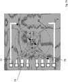
  • 1 einen schematischen nicht maßstabsgerechten Querschnitt durch eine Vorrichtung, die den erfindungsgemäßen mikromechanischen Sensor umfasst, längs der Schraubenachse,
  • 2 einen schematischen nicht maßstabsgerechten Querschnitt durch eine Vorrichtung, die den erfindungsgemäßen mikromechanischen Sensor umfasst, längs der Schraubenachse mit Aufsicht auf den Sensor bzw. Drucksensor und auf den Auswerteschaltkreis,
  • 3 die schematische nicht maßstabsgerechte Seitenansicht der Vorrichtung, die den erfindungsgemäßen mikromechanischen Sensor umfasst (korrespondiert mit 1),
  • 4 die schematische nicht maßstabsgerechte Seitenansicht der Vorrichtung, die den erfindungsgemäßen mikromechanischen Sensor umfasst, (korrespondiert mit 2),
  • 5 einen vereinfachten, schematischen und nicht maßstabsgerechten Querschnitt durch einen erfindungsgemäßen Drucksensor,
  • 6a einen vereinfachten, schematischen und nicht maßstabsgerechten Querschnitt durch einen erfindungsgemäßen Drucksensor, wobei dieser Gräben zur Verbindung mit einer Dichtung aufweist,
  • 6b eine vereinfachte, schematische und nicht maßstabsgerechte Aufsicht auf einen erfindungsgemäßen Drucksensor, wobei dieser Gräben zur Verbindung mit einer Dichtung aufweist,
  • 7 einen schematischen nicht maßstabsgerechten Querschnitt durch eine Vorrichtung, die den erfindungsgemäßen mikromechanischen Sensor umfasst, längs der Schraubenachse mit Aufsicht auf einen erfindungsgemäßen Drucksensors und auf den Auswerteschaltkreis, wobei der erfindungsgemäße Drucksensor eine Keilform hat um die Abdichtung zu verbessern,
  • 8 stellt die beispielhaften erfindungsgemäßen Drucksensoren in Keilform in schematischer nicht maßstabsgerechter Aufsicht im Wafer-Verbund dar,
  • 9 einen schematischen nicht maßstabsgerechten Querschnitt durch eine Vorrichtung, die den erfindungsgemäßen mikromechanischen Sensor umfasst, längs der Schraubenachse mit Aufsicht auf den beispielhaften erfindungsgemäßen Drucksensor und auf den Auswerteschaltkreis, wobei statt eines Gewindes eine Passung außen angebracht ist,
  • 10 einen schematischen nicht maßstabsgerechten Querschnitt durch eine Vorrichtung , die den erfindungsgemäßen mikromechanischen Sensor umfasst, längs der Schraubenachse mit Aufsicht auf den beispielhaften erfindungsgemäßen Drucksensor und auf den Auswerteschaltkreis, wobei statt eines Gewindes eine Passung außen angebracht ist und die Vorrichtung in die Öffnung einer Wand eingebaut ist und der Sensorbereich (erster Bereich A) des erfindungsgemäßen Drucksensors von einem zu messenden Medium umspült wird,
  • 11-21 ein beispielhaftes Fertigungsverfahren für ein Sensorsystem, das den erfindungsgemäßen mikromechanischen Sensor umfasst,
  • 11 einen Träger, der als Basis für das System, das den erfindungsgemäßen mikromechanischen Sensor umfasst, dient,
  • 12 den Träger aus 11 nach anbringen der zweiten Dichtung durch Ummolden,
  • 13 den Träger aus 12 nach Aufbringen der Kleber für den Auswerteschaltkreis und den erfindungsgemäßen Sensor,
  • 14 den Träger aus 13 nach dem Aufbringen (Die-Bond) des Auswerteschaltkreises,
  • 15 den Träger aus 14 nach dem Aufbringen (Die-Bond) des erfindungsgemäßen Sensors,
  • 16 den Träger aus 15 nach dem Bonden des Auswerteschaltkreises auf der Steckerseite,
  • 17 den Träger aus 16 nach dem Herstellen der elektrischen Verbindungen zwischen erfindungsgemäßem Sensor und Auswerteschaltkreis durch Bonden,
  • 18 das Sensorsystem nach Zusammenbau von Träger aus 17 und Sensorgehäuse,
  • 19 das Sensorsystem aus 18 nach dem Einbringen des Gels,
  • 20 das Sensorsystem aus 19 ergänzt um einen Dichtungsring,
  • 21 das Sensorsystem aus 20 verschlossen mit der ersten Dichtung,
  • 22 einen schematischer, nicht maßstabsgerechter Querschnitt durch einen erfindungsgemäßen Drucksensor ähnlich 5, wobei dieser auf beiden Seiten eines mikromechanischen Funktionselements Dichtungsbereiche aufweist,
  • 23 eine schematische, nicht maßstabsgerechte Aufsicht auf den erfindungsgemäßen beispielhaften Drucksensor entsprechend 22,
  • 24 einen schematischer Querschnitt durch ein beispielhaftes Gehäuse für den beispielhaften Drucksensor der Folien 22 und 23.
The invention is based on the 1 to 23 the example of a pressure sensor measuring system with a screw thread and the associated sensor, which is claimed here explained. Other configurations and designs are of course possible. It shows
  • 1 a schematic cross-section, not to scale, through a device comprising the micromechanical sensor according to the invention along the screw axis;
  • 2 a schematic not to scale cross section through a device, the micromechanical invention Sensor comprises, along the screw axis with a view of the sensor or pressure sensor and the evaluation circuit,
  • 3 the schematic not to scale side view of the device comprising the micromechanical sensor according to the invention (corresponds to 1 )
  • 4 the schematic not to scale side view of the device comprising the micromechanical sensor according to the invention (corresponds to 2 )
  • 5 a simplified, schematic and not to scale cross section through a pressure sensor according to the invention,
  • 6a a simplified, schematic and not to scale cross section through a pressure sensor according to the invention, said trenches for connection to a seal,
  • 6b a simplified, schematic and not to scale supervision of a pressure sensor according to the invention, said trenches for connection to a seal,
  • 7 a schematic not to scale cross-section through a device comprising the micromechanical sensor according to the invention, along the screw axis with a view of a pressure sensor according to the invention and the evaluation circuit, the pressure sensor according to the invention has a wedge shape to improve the seal,
  • 8th shows the exemplary pressure sensors according to the invention in wedge shape in a schematic not to scale supervision in the wafer composite,
  • 9 a schematic not to scale cross section through a device comprising the micromechanical sensor according to the invention, along the screw axis with a view of the exemplary pressure sensor according to the invention and the evaluation circuit, wherein instead of a thread, a fit is attached to the outside,
  • 10 a schematic not to scale cross section through a device comprising the micromechanical sensor according to the invention, along the screw axis with a view of the exemplary pressure sensor according to the invention and the evaluation circuit, instead of a thread, a fit is mounted outside and the device is installed in the opening of a wall and the sensor area (first area A) of the pressure sensor according to the invention is surrounded by a medium to be measured,
  • 11-21 an exemplary manufacturing method for a sensor system comprising the micromechanical sensor according to the invention,
  • 11 a support which serves as the basis for the system comprising the micromechanical sensor according to the invention,
  • 12 the carrier off 11 after attaching the second seal by Ummolden,
  • 13 the carrier off 12 after application of the adhesive for the evaluation circuit and the sensor according to the invention,
  • 14 the carrier off 13 after the application (die bond) of the evaluation circuit,
  • 15 the carrier off 14 after the application (die bond) of the sensor according to the invention,
  • 16 the carrier off 15 after bonding the evaluation circuit on the plug side,
  • 17 the carrier off 16 after establishing the electrical connections between sensor according to the invention and evaluation circuit by bonding,
  • 18 the sensor system after assembly of carrier 17 and sensor housing,
  • 19 the sensor system off 18 after the introduction of the gel,
  • 20 the sensor system off 19 supplemented by a sealing ring,
  • 21 the sensor system off 20 closed with the first seal,
  • 22 a schematic, not to scale cross section through a pressure sensor according to the invention similar 5 wherein this has sealing regions on both sides of a micromechanical functional element,
  • 23 a schematic, not to scale supervision on the exemplary pressure sensor according to the invention accordingly 22 .
  • 24 a schematic cross section through an exemplary housing for the exemplary pressure sensor of the films 22 and 23 ,

Es ist von besonderem Vorteil, wenn das Sensorsystem in Form einer M5 oder M10 Schraube ausgeführt werden kann. Dies ist in 1 nicht maßstabsgerecht dargestellt. Die Schraube ist mit einem Gewinde (1) und einem Schraubenkopf (32) versehen. Dem Fachmann ist klar, dass unter Gewinde in diesem Sinne auch ähnliche Maschinenelemente verstanden werden können, die zu einer Verbindung zwischen einem Loch in einem Werkstück und dem Drucksensorsystem führen können. Solche Maschinenelemente können beispielsweise auch Presspassungen und BajonettVerschlüsse, eine Gleitpassung für und Klebe-, Schweiß- oder Lötverbindungen eine Bolzenaußenfläche für eine Bolzenverbindung und eine Keilaußenfläche für eine Keilverbindung etc. sein.It is of particular advantage if the sensor system can be designed in the form of an M5 or M10 screw. This is in 1 not shown to scale. The screw is threaded ( 1 ) and a screw head ( 32 ) Mistake. It will be clear to a person skilled in the art that threads in this sense can also be understood as meaning similar machine elements which can lead to a connection between a hole in a workpiece and the pressure sensor system. Such machine elements may also be, for example, press fits and bayonet locks, a slip fit for and glued, welded or soldered joints, a bolt outer surface for a bolted joint and a wedge outer surface for a keyed joint, etc.

Die weitere Beschreibung bezieht sich auf eine Schraube mit einem Gewinde. In den Ansprüchen wird demgegenüber jedoch von einem Maschinenelement zur Verbindung mit einer Öffnung gesprochen.The further description refers to a screw with a thread. In the claims, however, is spoken by a machine element for connection to an opening.

Wenn von einer Achse des Maschinenelements zur Verbindung zur Verbindung mit einer Öffnung die Rede ist, so ist damit eine Linie gemeint längs derer das Sensorgehäuse bei der Montage an einen bestimmungsgemäßen Verwendungsort bewegt wird. Eine Schraube wird beispielsweise längs der Schraubengewindeachse in eine Öffnung hineingedreht. Dabei bewegt sich die Schraube längs dieser besagten Achse des Maschinen Elements zur Verbindung zur Verbindung mit einer Öffnung (Gewindeachse) in die Montageöffnung hinein. Handelt es sich um eine Passung, so wird das Sensorgehäuse unter Umständen ohne Drehung in die Montageöffnung hineinbewegt.When talking about an axis of the machine element for connection to the connection with an opening, it is meant a line along which the sensor housing is moved during assembly to a designated place of use. For example, a screw is screwed into an opening along the screw thread axis. In this case, the screw moves along this said axis of the machine element for connection to the connection with an opening (threaded axis) into the mounting opening. If it is a fit, the sensor housing may be moved into the mounting hole without rotation.

Zum Zwecke des besseren Verständnisses wird hier nur eine Schraube behandelt. Dem Fachmann werden die Modifikationen offensichtlich sein, die für die Verwendung anderer Befestigungstechniken erforderlich sind.For the purpose of better understanding only one screw is treated here. the Persons skilled in the art will be aware of the modifications required for the use of other fastening techniques.

Die Schraube kann bei Bedarf selbstverständlich länger gewählt werden. Die Position des Schraubenkopfes (32) kann auf der Längsachse der Schraube (37) ebenso anders gewählt werden. Der Schraubenkopf (32) ist beispielsweise mit einer umlaufenden Nut (31) versehen, die einen Dichtungsring (30) aufnimmt. Hierdurch kann das Drucksensorgehäuse druckdicht beispielsweise durch eine einfache M5- oder M10-Bohrung an einen Druckkörper angebracht werden. The screw can of course be chosen longer if necessary. The position of the screw head ( 32 ) can on the longitudinal axis of the screw ( 37 ) are chosen differently. The screw head ( 32 ) is, for example, with a circumferential groove ( 31 ) provided with a sealing ring ( 30 ). As a result, the pressure sensor housing pressure-tight, for example, be attached by a simple M5 or M10 bore to a pressure hull.

Die Schraube ist mit einer Längsbohrung (2) ausreichender Weite versehen. Der Durchmesser des Drucksensorgehäuses und Bohrungsdurchmesse müssen geeignet gewählt werden.The screw is with a longitudinal bore ( 2 ) provided sufficient width. The diameter of the pressure sensor housing and bore diameter must be selected appropriately.

Das Drucksensorgehäuse (100) ist darüber hinaus typischerweise innen mit zwei umlaufenden Nuten versehen. Die erste Nut (10) sorgt für eine mechanische Verbindung zwischen der ersten Dichtung (11) an der Medienseite und dem Drucksensorgehäuse (100). Die zweite Nut (33) fixiert die zweite Dichtung (34) zum Verschluss des Sensorgehäuses (100) auf der elektrischen Kontaktseite. Hierdurch kann die Elektronik durch das zu vermessende Medium (73, 10) unter Druck nicht herausgedrückt werden.The pressure sensor housing ( 100 ) is also typically provided internally with two circumferential grooves. The first groove ( 10 ) provides a mechanical connection between the first seal ( 11 ) on the media side and the pressure sensor housing ( 100 ). The second groove ( 33 ) fixes the second seal ( 34 ) to the closure of the sensor housing ( 100 ) on the electrical contact side. This allows the electronics through the medium to be measured ( 73 . 10 ) can not be pushed out under pressure.

Kern der Vorrichtung ist ein Träger (18), beispielsweise eine Platine (PCB), die den eigentlichen mikromechanischen Sensor (3), beispielsweise einen MEMS Drucksensor, und den Auswerteschaltkreis (IC) (21) trägt. Statt eines PCBs, das typischerweise aus einem Verbundmaterial besteht, ist natürlich auch die Verwendung eines MID-Lead-Frames denkbar. Auch können andere isolierende organische oder anorganische Substrate verwendet werden. Solche können beispielsweise aus einer Keramik oder einem Glasträger oder einem mono- nano- oder poly-kristallinen Wide-Bandgap-Material wie beispielsweise Saphir, bestehen. Auch ist die Verwendung von leitenden oder halbleitenden Materialien als Trägermaterial denkbar. Diese müssen jedoch zumindest einseitig isolierend beschichtet werden. Wenn im Folgenden und in den Ansprüchen von „Träger“ gesprochen wird, sind daher auch solche Konstruktionen, wie z.B. die skizzierten, eingeschlossen, die der Funktion eines PCBs gleich- oder nahekommen. Darüber hinaus weist der besagte Träger (18) verschiedene Leiterbahnen (36) und leitende Inseln (19) und (17) auf, die zur Befestigung des Auswerteschaltkreises (21) und des mikromechanischen Sensors (3), beispielsweise eines MEMS-Drucksensors, dienen. Für die Herstellung solcher Metallinseln sind aus dem Stand der Technik mannigfache Verfahren bekannt, die hier nicht weiter beschrieben sind, da sie dem Fachmann offensichtlich sind.The core of the device is a carrier ( 18 ), for example, a board (PCB), the actual micromechanical sensor ( 3 ), for example a MEMS pressure sensor, and the evaluation circuit (IC) ( 21 ) wearing. Instead of a PCB, which typically consists of a composite material, of course, the use of an MID lead frame is conceivable. Also, other insulating organic or inorganic substrates can be used. Such may, for example, consist of a ceramic or a glass carrier or a mono- or poly-crystalline wide-bandgap material such as sapphire. The use of conductive or semiconductive materials as a carrier material is also conceivable. However, these must be coated on at least one side insulating. Therefore, when "carrier" is used in the following and in the claims, such constructions as those outlined are included, which are similar or approximate to the function of a PCB. In addition, the said carrier ( 18 ) different tracks ( 36 ) and conductive islands ( 19 ) and ( 17 ), which are used for fastening the evaluation circuit ( 21 ) and the micromechanical sensor ( 3 ), for example a MEMS pressure sensor. For the production of such metal islands, various methods are known from the prior art, which are not further described here, since they are obvious to the person skilled in the art.

Der mikromechanische Drucksensor (3) ist typischerweise mit einem Kleber (16) auf der Befestigungsfläche (17) für den mikromechanischen Drucksensor (3) befestigt, die sich auf dem Träger (18) befindet.The micromechanical pressure sensor ( 3 ) is typically with an adhesive ( 16 ) on the mounting surface ( 17 ) for the micromechanical pressure sensor ( 3 ) mounted on the support ( 18 ) is located.

Ebenso ist der Auswerteschaltkreis (21) mit einem ähnlichen oder gleichen Kleber (20) auf einer analogen Befestigungsfläche (19) für den Auswerteschaltkreis (21) auf dem Träger (18), z.B. einem PCB, befestigt.Likewise, the evaluation circuit ( 21 ) with a similar or identical adhesive ( 20 ) on an analogous mounting surface ( 19 ) for the evaluation circuit ( 21 ) on the support ( 18 ), eg a PCB.

Der mikromechanische Drucksensor (3 ist auf der Medienseite so von einer ersten Dichtung (11) umschlossen, dass kein Medium an der Grenzfläche zwischen mikromechanischem Drucksensor (3) und erster Dichtung (11) sowie erster Dichtung (11) und Sensorgehäuse (100) durchtreten kann. Das Material der ersten Dichtung (11) füllt dabei auch die erste Nut (10) des Sensorgehäuses (100) so aus, dass diese Nut (10) vorzugsweise mit dem Material der ersten Dichtung ebenfalls gefüllt wird. Hierdurch ist der Mediendruck nicht in der Lage, die erste Dichtung (10) ins Innere des Sensorgehäuses zu drücken.The micromechanical pressure sensor ( 3 is on the media side so from a first seal ( 11 ) that no medium at the interface between micromechanical pressure sensor ( 3 ) and first seal ( 11 ) as well as first seal ( 11 ) and sensor housing ( 100 ) can pass through. The material of the first seal ( 11 ) fills the first groove ( 10 ) of the sensor housing ( 100 ) so that this groove ( 10 ) is preferably also filled with the material of the first seal. As a result, the media pressure is not able, the first seal ( 10 ) into the interior of the sensor housing.

Der mikromechanische Drucksensor (3) durchdringt diese erste Dichtung (11) in der Art, dass zum einen die eigentliche Messzelle (erster Bereich A 5) weit genug von der ersten Dichtung (11) entfernt liegt und von deren Material nicht bedeckt wird. Die Messzelle des Drucksensors besteht beispielsweise aus der evakuierten Drucksensorkavität (71), den Piezo-Widerständen (50, 51, 52, 53) und wesentlichen Teilen der Zuleitungen (6, 9). Die erste Dichtung (11) umschließt den mikromechanischen Drucksensor (3) in einem zweiten Bereich (zweiter Bereich B 5) in dem der mikromechanische Drucksensor (3) vorzugsweise keine Metallisierungen oder Funktionselemente insbesondere auf der Oberfläche des mikromechanischen Drucksensors (6) aufweist, die mikromechanischer Natur sind oder die aus Materialien gefertigt sind, die durch das zu messende Medium korrodiert oder beeinflusst werden können.The micromechanical pressure sensor ( 3 ) penetrates this first seal ( 11 ) in such a way that on the one hand, the actual measuring cell (first area A 5 ) far enough from the first seal ( 11 ) is removed and is not covered by their material. The measuring cell of the pressure sensor consists for example of the evacuated pressure sensor cavity ( 71 ), the piezo resistors ( 50 . 51 . 52 . 53 ) and essential parts of the supply lines ( 6 . 9 ). The first seal ( 11 ) encloses the micromechanical pressure sensor ( 3 ) in a second area (second area B 5 ) in which the micromechanical pressure sensor ( 3 ) preferably no metallizations or functional elements, in particular on the surface of the micromechanical pressure sensor ( 6 ), which are micromechanical in nature or made of materials that can be corroded or influenced by the medium to be measured.

Dieser zweite Bereich (B) ist in der WO 2011/ 083 161 A2 nicht offenbart, die lediglich davon spricht, dass die Zuleitungen der piezo-resitiven Widerstände möglichst in Silizium ausgeführt werden sollen (Seite 15 Zeilen 7 bis 11 der WO 2011/ 083 161 A2 ) und/oder die Bond-Pads maximal weit von den piezo-resitiven Sensorelementen zu entfernen (Seite 20 Zeilen 16 bis 21 der WO 2011/ 083 161 A2 ). Die WO 2011/ 083 161 A2 zeigt hierbei insbesondere nicht, dass ein solcher metallfreier zweiter Bereich (B) zwischen den mikromechanischen Funktionselementen zur Druckmessung im ersten Bereich (A) und dem Bondsystem in einem dritten Bereich (C) liegen muss, der der Abdichtung dient. Dabei kann das Medium, beispielsweise das Öl eines Verbrennungsmotors, insbesondere auch in verunreinigter Form, also beispielsweise mit einem signifikant abweichenden pH-Wert, vorliegen und die Beeinflussung oder die Korrosion durch die Verunreinigungen verursacht werden. Im Falle von Öl eines Verbrennungsmotors als Medium können solche Verunreinigungen beispielsweise Säuren etc. sein, die durch die Verbrennung im Brennraum des Motors entstehen.This second area ( B ) is in the WO 2011/083 161 A2 not disclosed, which only speaks of the fact that the leads of the piezo-resistive resistors should be performed as possible in silicon (page 15 row 7 to 11 of the WO 2011/083 161 A2 ) and / or to remove the bond pads as far as possible from the piezo-resistive sensor elements (page 20 row 16 to 21 of the WO 2011/083 161 A2 ). The WO 2011/083 161 A2 in particular does not show that such a metal-free second region ( B ) between the micromechanical functional elements for pressure measurement in the first region ( A ) and the bond system in a third area ( C ), which serves the sealing. In this case, the medium, for example, the oil of an internal combustion engine, especially in contaminated form, so for example, with a significantly different pH, are present and the influence or corrosion caused by the impurities. In the case of oil of an internal combustion engine as a medium such impurities may be, for example, acids, etc., which are formed by the combustion in the combustion chamber of the engine.

Der mikromechanische Drucksensor, weist dabei ein Zwischenoxid (5, 5) auf, das die piezo-resitiven Widerstände (50, 51, 52, 53) bedeckt und selbst wieder mit einer Schutzschicht beispielsweise aus Poly-Silizium (4, 5) bedeckt ist. Mit Poly-Silizium wird im Folgenden und auch hier polykristallines Silizium bezeichnet. Diese Schicht (4) bedeckt auch die Membrane (7, 5) der Druckmesszelle (8). Hierdurch wird die im aggressiven Medium befindliche Druckmesszelle (8) vor dem zu vermessenden Medium geschützt.The micromechanical pressure sensor has an intermediate oxide ( 5 . 5 ), the piezo-resistive resistors ( 50 . 51 . 52 . 53 ) and again with a protective layer, for example made of poly-silicon ( 4 . 5 ) is covered. Poly-silicon is referred to below and here polycrystalline silicon. This layer ( 4 ) also covers the membrane ( 7 . 5 ) of the pressure measuring cell ( 8th ). As a result, the pressure measuring cell located in the aggressive medium ( 8th ) protected from the medium to be measured.

Es ist denkbar, statt oder zusätzlich zu dieser Schicht (4, 5) auch andere Schichten wie beispielsweise SiN zu benutzen. Auch kann eine ausreichend dicke Ausführung des Oxids (5, 5) für den jeweiligen Anwendungszweck bereits genügend Schutz bieten. In diesem Fall kann die Schicht (4, 5) ggf. sogar entfallen. SiN bietet den Vorteil, die Diffusion von Wasserstoff zu reduzieren.It is conceivable, instead of or in addition to this layer ( 4 . 5 ) to use other layers such as SiN. Also, a sufficiently thick version of the oxide ( 5 . 5 ) already provide sufficient protection for the respective application. In this case, the layer ( 4 . 5 ) possibly even omitted. SiN offers the advantage of reducing the diffusion of hydrogen.

Auf der anderen Seite der ersten Dichtung (11) liegen die Kontakte (13) des mikromechanischen Drucksensors (dritter Bereich C, 5) frei. Die erste Dichtung (11) befindet sich also nur in einem Zwischenbereich (zweiter Bereich B 5) zwischen Kontakten (13) (dritter Bereich C 5) und Sensormesszelle (8, 7) (erster Bereich A 5).On the other side of the first seal ( 11 ) are the contacts ( 13 ) of the micromechanical pressure sensor (third area C . 5 ) free. The first seal ( 11 ) is thus located only in an intermediate area (second area B 5 ) between contacts ( 13 ) (third area C 5 ) and sensor measuring cell ( 8th . 7 ) (first area A 5 ).

Um den mikromechanischen Drucksensor, kontaktieren zu können, ist die Zwischenoxidschicht (5) im Bereich der Kontakte (13) (dritter Bereich C 5) geöffnet. Diese Öffnungen (13) sind mit dem Bond-Pad-Metall (14) bedeckt, um Bondbarkeit herstellen zu können.In order to be able to contact the micromechanical pressure sensor, the intermediate oxide layer ( 5 ) in the area of contacts ( 13 ) (third area C 5 ) open. These openings ( 13 ) are bonded to the bond pad metal ( 14 ) to make bondability.

Bonddrähte (15) verbinden den Auswerteschaltkreis (21) mit dem mikromechanischen Drucksensor (3). Die Bondung kann dabei beispielsweise so geschehen, dass der Bond-Ball (22) auf dem Auswerteschaltkreis (21) abgesetzt wird und der Wedge-Bond auf der Kontaktfläche (14) des mikromechanischen Drucksensors (3).Bonding wires ( 15 ) connect the evaluation circuit ( 21 ) with the micromechanical pressure sensor ( 3 ). The bonding can for example be done so that the bond ball ( 22 ) on the evaluation circuit ( 21 ) and the wedge bond on the contact surface ( 14 ) of the micromechanical pressure sensor ( 3 ).

Zur Vereinfachung sind die Schaltungen des Auswerteschaltkreises (21) nur vereinfacht (24) eingezeichnet. Auch der Auswerteschaltkreis (21) ist durch ein Oxid und eine Passivierung (25) geschützt. Der Auswerteschaltkreis (21) verfügt über geeignete Bond-Flächen (26, 23), um einen elektrischen Anschluss zu ermöglichen.For simplicity, the circuits of the evaluation circuit ( 21 ) only simplified ( 24 ). Also the evaluation circuit ( 21 ) is characterized by an oxide and a passivation ( 25 ) protected. The evaluation circuit ( 21 ) has suitable bond areas ( 26 . 23 ) to allow electrical connection.

Der Bond-Ball (22) des Bonddrahts (15) wird auf einem solchen Bond-Pad (23) des Auswerteschaltkreises (21) abgesetzt.The Bond Ball ( 22 ) of the bonding wire ( 15 ) is deposited on such a bond pad ( 23 ) of the evaluation circuit ( 21 ) discontinued.

Die Verbindung des Auswerteschaltkreises (21) nach Außen wird durch einen weiteren Bond-Draht (28) zwischen Auswerteschaltkreis (21) und Leiterbahn (36) auf dem Träger (18) hergestellt. In dem Beispiel wird der zugehörige Wedge-Bond (29) auf der Leiterbahn (36) und der Bond-Ball (27) auf dem Auswerteschaltkreis (21) gefertigt.The connection of the evaluation circuit ( 21 ) to the outside by another bond wire ( 28 ) between evaluation circuit ( 21 ) and conductor track ( 36 ) on the support ( 18 ) produced. In the example, the associated wedge-bond ( 29 ) on the track ( 36 ) and the bond ball ( 27 ) on the evaluation circuit ( 21 ).

Der Innenraum des Sensorgehäuses (100) wird auf der medienabgewandten Seite durch eine weitere Dichtung (34) abgedichtet. Diese reicht in diesem Beispiel wie bereits die erste Dichtung (11) auf der Medienseite bis in eine zweite umlaufende Nut (33) hinein.The interior of the sensor housing ( 100 ) is on the side facing away from the media by another seal ( 34 ) sealed. This extends in this example as already the first seal ( 11 ) on the media side into a second circumferential groove ( 33 ) into it.

Diese Dichtung (34) wird durch das PCB (18) und die Verdrahtung (19) durchdrungen. Die außenliegenden Teile der Verdrahtung (36) des PCBs (35) können vergoldet werden und als Stecker (36) verwendet werden.This seal ( 34 ) is passed through the PCB ( 18 ) and the wiring ( 19 ). The external parts of the wiring ( 36 ) of the PCB ( 35 ) can be gold plated and used as a plug ( 36 ) be used.

Das Innere des Sensorgehäuses (100) ist vorzugsweise mit einem Gel (12) gefüllt, um die mechanischen Einflüsse zu minimieren und den Auswerteschaltkreis (21) und das Bondsystem zu schützen.The interior of the sensor housing ( 100 ) is preferably with a gel ( 12 ) in order to minimize the mechanical influences and the evaluation circuit ( 21 ) and to protect the bond system.

2 zeigt ebenfalls einen Querschnitt durch die Sensorschraube. Nun jedoch sind der Träger (18), der Auswerteschaltkreis (21) und der mikromechanische Drucksensor (3) in Aufsicht dargestellt. 2 also shows a cross section through the sensor screw. Now, however, the carrier ( 18 ), the evaluation circuit ( 21 ) and the micromechanical pressure sensor ( 3 ) shown in supervision.

Der außenliegende Platinenstecker besteht in diesem Beispiel aus vier Leitungen (38, 39, 40, 41). Dies können beispielsweise eine positive Spannungsversorgung, ein Masseanschluss und zwei Datenleitungen - beispielsweise Takt und bidirektionale Daten- oder RX- und TX-Leitungen sein.The external board connector consists in this example of four lines ( 38 . 39 . 40 . 41 ). These may be, for example, a positive voltage supply, a ground connection and two data lines - for example clock and bidirectional data or RX and TX lines.

Diese vier Leitungen (38, 39, 40, 41) sind mit vier Bonddrähten (42, 43, 44, 45) mit dem Auswerteschaltkreis (21) verbunden. Der Auswerteschaltkreis (21) ist mit einem Kleber (20) auf der Befestigungsfläche (19) befestigt, das Teil der gedruckten Schaltung (18) ist.These four lines ( 38 . 39 . 40 . 41 ) are equipped with four bonding wires ( 42 . 43 . 44 . 45 ) with the evaluation circuit ( 21 ) connected. The evaluation circuit ( 21 ) is with an adhesive ( 20 ) on the mounting surface ( 19 ), the part of the printed circuit ( 18 ).

Auf der dem Medium zugewandten Seite ist der Auswerteschaltkreis (21) mit vier Bond-Drähten (46, 47, 48, 49) mit dem mikromechanischen Drucksensor (3), einem beispielhaften Drucksensor, verbunden. Diese vier Verbindungen stellen beispielsweise eine Masseverbindung, die Spannungsversorgung und die beiden Ausgänge einer Wheatstone-Brücke dar.On the side facing the medium is the evaluation circuit ( 21 ) with four bond wires ( 46 . 47 . 48 . 49 ) with the micromechanical pressure sensor ( 3 ), an exemplary pressure sensor. These four connections represent, for example, a ground connection, the power supply and the two outputs of a Wheatstone bridge.

Diese Wheatstone-Brücke besteht in diesem Beispiel aus den piezoresistiven Widerständen (50, 51, 52, 53), die zu dieser Wheatstonebrücke verschaltet sind.This Wheatstone bridge consists in this example of the piezoresistive resistors ( 50 . 51 . 52 . 53 ), which are connected to this Wheatstone bridge.

Die Widerstände (50, 51, 52, 53) sind, wie bei piezoresistiven Drucksensoren üblich, geeignet über einer Drucksensormembrane (7) platziert.The resistors ( 50 . 51 . 52 . 53 ) are, as usual in piezoresistive pressure sensors, suitable over a pressure sensor membrane ( 7 ).

Der mikromechanische Drucksensor (3) ist mit Kleber (16) auf der Befestigungsfläche (17) befestigt, die Teil des Trägers (18) ist.The micromechanical pressure sensor ( 3 ) is with glue ( 16 ) on the mounting surface ( 17 ), the part of the carrier ( 18 ).

In 2 ist zu erkennen, dass die erste Dichtung (11) wiederum die Sensorzelle (8), hier eine Drucksensorzelle, und die Bondflächen des mikromechanischen Drucksensors (3) freilässt.In 2 it can be seen that the first seal ( 11 ) again the sensor cell ( 8th ), here a pressure sensor cell, and the bonding surfaces of the micromechanical pressure sensor ( 3 ).

3 und 4 zeigen das Sensorgehäuse (100) von der Seite in den Ansichten, die den 1 und 2 entsprechen. 3 and 4 show the sensor housing ( 100 ) from the page in the views that the 1 and 2 correspond.

5 zeigt in einem vereinfachten, nicht maßstabsgerechten Querschnitt durch den mikromechanischen Drucksensor (3). Weiter zeigt 5 die Bereiche A, B und C. Insbesondere ist Abschnitt B stark verkürzt und die vertikalen Dimensionen der Schichten sind vergrößert, während die Dicke des Sensors (4) verkleinert dargestellt ist. Es handelt sich also nur um eine Veranschaulichung der wesentlichen Merkmale für einen Fachmann. 5 shows in a simplified, not to scale cross section through the micromechanical pressure sensor ( 3 ). Next shows 5 the areas A . B and C , In particular, section is B greatly shortened and the vertical dimensions of the layers are increased while the thickness of the sensor ( 4 ) is shown in reduced size. It is therefore only an illustration of the essential features for a person skilled in the art.

In diesem Beispiel (siehe 5) handelt es sich um einen Drucksensor in Buried-Cavity-Technologie. Hierbei wird in einen Handle-Wafer (62), der mit einer Oxidschicht (60) versehen ist, eine Vertiefung (57) fotolithografisch eingeätzt. Nach einer Reinigung wird ein Device-Wafer (61) auf den Handle-Wafer gebondet und durch mechanisches und chemisches Polieren soweit abgedünnt, bis die Dicke des Device-Wafer-Materials über der somit gebildeten Kavität (71), also der Membrane (7), der Zielmembrandicke entspricht.In this example (see 5 ) is a pressure sensor in Buried Cavity technology. This is done in a handle wafer ( 62 ) coated with an oxide layer ( 60 ), a recess ( 57 ) etched photolithographically. After cleaning, a device wafer ( 61 ) bonded to the handle wafer and thinned by mechanical and chemical polishing until the thickness of the device wafer material over the thus formed cavity ( 71 ), ie the membrane ( 7 ) corresponding to the target membrane thickness.

Prozesse zur Fertigung solcher Sensoren sind beispielsweise in der WO 2011/ 083 161 A2 beschrieben.Processes for the production of such sensors are for example in the WO 2011/083 161 A2 described.

Der Querschnitt zeigt vereinfacht die piezoresistiven p- Widerstände (53) und (50). Diese werden über hochdotierte p+-Halbleitergebiete (6, 9, 57, 58, 59) angeschlossen.The cross section shows the piezoresistive p-resistances ( 53 ) and ( 50 ). These are generated via highly doped p + semiconductor regions ( 6 . 9 . 57 . 58 . 59 ) connected.

Es ist besonders vorteilhaft und der wesentliche erfinderische Gedanke dieser Offenbarung, wenn in dem Bereich der ersten Dichtung (zweiter Bereich B) und im Bereich der Sensorzelle (erster Bereich A) ausschließlich solche dotierten Gebiete zum Anschluss der Sensormesszelle (8) benutzt werden. Dies hat thermomechanische Vorteile und Vorteile des Korrosionsschutzes, da Silizium erheblich widerstandsfähiger gegen viele korrosive Stoffe ist.It is particularly advantageous and the essential inventive idea of this disclosure, if in the area of the first seal (second area B ) and in the area of the sensor cell (first area A ) exclusively such doped regions for connecting the sensor measuring cell ( 8th ) to be used. This has thermo-mechanical advantages and advantages of corrosion protection, since silicon is considerably more resistant to many corrosive substances.

Die Druckmesszelle (8) ist mit einem dünnen Oxid (56) von typischerweise 2nm bis 40nm bedeckt. Im Bereich der piezoresistiven Widerstände (53) und (50) sind diese vorzugsweise zumindest teilweise jeweils durch einen Poly-Silizium-Schild (55) und (54) bedeckt, der den jeweiligen piezoresistiven Widerstand (53) und (50) schützt. Die Konstruktion wird typischerweise durch ein weiteres Oxid (5) zumindest teilweise abgedeckt. Es ist bekannt, dass es vorteilhaft ist, die Membrane (7) von der Bedeckung durch dieses Oxid (5) auszusparen oder das Oxid in diesem Bereich verdünnt zu fertigen. Dies ist in 5 allerdings zur Vereinfachung so nicht gezeichnet.The pressure measuring cell ( 8th ) is with a thin oxide ( 56 ) of typically 2nm to 40nm. In the field of piezoresistive resistors ( 53 ) and ( 50 ) are preferably at least partially each by a poly-silicon shield ( 55 ) and ( 54 ), the respective piezoresistive resistance ( 53 ) and ( 50 ) protects. The construction is typically characterized by another oxide ( 5 ) at least partially covered. It is known that it is advantageous to use the membrane ( 7 ) from the covering by this oxide ( 5 ) or to make the oxide diluted in this area. This is in 5 however not so drawn for the sake of simplicity.

Die Sensormesszelle ist soweit mit Poly-Silizium (4) abgedeckt, dass ein Zugriff aggressiver Chemikalien nicht möglich ist. Dieses Merkmal der ganzflächigen Abdeckung der Sensorzelle mit Poly-Silizium (4) ist in der US 8 049 290 B2 ( US 2009/ 0 206 467 A1 ) und der WO 2011/ 083 161 A2 so nicht offenbart und stellt einen erfindungsgemäßen Unterschied zum Stand der Technik dar. Die WO 2011/ 083 161 A2 zeigt lediglich die lokale Abdeckung der Piezo-Widerstände mit einer ersten Poly-Silizium-Struktur, die den Poly-Silizium-Schilden (54, 55) entspricht. Diese Abdeckung (4) mit gleichem thermischen Ausdehnungskoeffizienten wir die Membrane, unterdrückt zusätzlich eine durch ein elektrisches Feld getriebene Ionen-Diffusion.The sensor cell is so far with poly-silicon ( 4 ) that access of aggressive chemicals is not possible. This feature of full-area coverage of the sensor cell with poly-silicon ( 4 ) is in the US 8 049 290 B2 ( US 2009/0 206 467 A1 ) and the WO 2011/083 161 A2 so not disclosed and represents a difference according to the invention to the prior art. The WO 2011/083 161 A2 shows only the local coverage of the piezo-resistors with a first poly-silicon structure, the poly-silicon shields ( 54 . 55 ) corresponds. This cover ( 4 ) with the same thermal expansion coefficient as the membrane, in addition suppresses ion diffusion driven by an electric field.

Wie bereits oben beschrieben, ist die Verwendung anderer Materialien für diese Schicht (4) denkbar. Auch ist eine Kombination verschiedener Korrosionsschutzschichten denkbar. Eine wichtige Funktion des verwendeten Schichtstapels ist beispielsweise der Schutz vor dem Eindringen von Protonen, beispielsweise aus Feuchtigkeit, was ansonsten zu einer Drift der piezoresistiven Widerstände führen kann.As already described above, the use of other materials for this layer ( 4 ) conceivable. Also a combination of different corrosion protection layers is conceivable. An important function of the layer stack used is, for example, the protection against the penetration of protons, for example from moisture, which otherwise can lead to a drift of the piezoresistive resistors.

Am anderen Ende sind die p+-Zuleitungen (9) durch Kontakte (14) so zugänglich gemacht, dass eine Bondung möglich ist. (dritter Bereich C, 5)At the other end are the p + feeders ( 9 ) through contacts ( 14 ) so accessible that bonding is possible. (third area C . 5 )

In der Regel ist eine Kompensation des Temperaturgangs der Druckmesszelle erforderlich. Daher ist eine Temperaturmessung in unmittelbarer Nähe der Druckmesszelle sinnvoll. Hierfür ist es im Falle eines piezoresistiven Drucksensors vorteilhaft, eine Struktur ähnlich den Widerstandsstrukturen, die als piezoresistive Widerstände der Wheatstone-Brücke des erfindungsgemäßen Drucksensors verwendet werden, für die Temperaturmessung zu benutzen. Im einfachsten Fall wird ein solcher piezoresistiver Widerstand zusätzlich in den Bereich A (siehe 6) platziert mit dem Unterschied, dass dieser möglichst weit von allen Kanten incl. der Membrane platziert wird, um mechanischen Stress als beeinflussenden Faktor auszuschließen. Eine Ausprägung des erfindungsgemäßen Systems kann sich also auch durch einen zusätzlichen Temperatursensor oder eine zusätzliche Temperatursensorzelle, die typischerweise im Bereich A angeordnet wird, auszeichnen. Somit weist ein solches Sensorsystem, als besondere Ausprägung des erfindungsgemäßen Sensorsystems, mindestens zwei Sensoren und/oder mindestens zwei Sensorzellen auf wobei entweder zumindest einer der Sensoren ein Temperatursensor ist oder zumindest eine Sensorzelle eine Temperatursensorzelle ist und entweder zumindest ein Sensor (3) ein Drucksensor ist oder zumindest eine Sensorzelle (8) eine Drucksensorzelle ist.As a rule, a compensation of the temperature range of the pressure measuring cell is required. Therefore, a temperature measurement in the immediate vicinity of the pressure measuring cell makes sense. For this purpose, in the case of a piezoresistive pressure sensor, it is advantageous to use a structure similar to the resistance structures, which are used as piezoresistive resistors of the Wheatstone bridge of the pressure sensor according to the invention, for the temperature measurement. In the simplest case, such a piezoresistive resistor is additionally in the range A (please refer 6 ) with the difference that it is placed as far as possible from all edges including the membrane in order to exclude mechanical stress as an influencing factor. A Expression of the system according to the invention can therefore also by an additional temperature sensor or an additional temperature sensor cell, which typically in the field A is arranged, distinguished. Thus, such a sensor system, as a special feature of the sensor system according to the invention, at least two sensors and / or at least two sensor cells on either at least one of the sensors is a temperature sensor or at least one sensor cell is a temperature sensor cell and either at least one sensor ( 3 ) is a pressure sensor or at least one sensor cell ( 8th ) is a pressure sensor cell.

Da die Temperatursensorzelle vorzugsweise im Bereich A, in dem kein Metall verwendet werden sollte, platziert wird, ist es notwendig, diese Temperatursensorzelle, genau wie beim zuvor beschriebenen Anschluss der Drucksensormesszelle, vorzugsweise durch hochdotierte p+-Halbleiterleitungen anzuschließen und diese wie bei der Druckmesszelle bis in den Bereich C zu führen, wo der elektrische Anschluss bzw. die elektrische Verbindung mit dem Auswerteschaltkreis über Bond-Pads, also ein Metall-System, erfolgen kann. Dabei sollte diese Temperatursensorzelle, die typischerweise ein piezoresistiver Widerstand ist, in einer eigenen Wanne platziert werden. Beispielsweise ist es denkbar den Sensor (3) in einem p-dotierten Substrat auszuführen und die Widerstände in n-Wannen zu legen. Bei den Widerständen würde es sich dann um p-dotierte Widerstände handeln. Die Zuleitungen aller Widerstände incl. der Messwiderstände der Druckzelle würden dann in der jeweiligen p-Wanne als hochdotierte p+-Leitungen ausgeführt. Natürlich ist bei Verwendung eines n-leitenden Substrates die Nutzung der inversen Leitungstypen sinnvoll (p-Wanne, n-Widerstände, n+-Zuleitungen). Bei den Zuleitungen der Temperatursensorzelle wäre es sinnvoll diese Zuleitungen als Kelvin-Verdrahtung auszuführen. Dies erfordert an jedem Widerstandsanschluss zwei Leitungen, von denen jeweils eine zur Zuführung des elektrischen Stromes an den jeweiligen Kontakt genutzt würde und die andere zur Vermessung des Potenzials. Somit sind insgesamt vier solcher hochdotierten Halbleiterleitungen für den Anschluss einer Temperatursensorzelle erforderlich. Diese Konstruktion hat den Vorteil, dass Leckströme der p+-Zuleitungen in die n-Wanne hinein das Messergebnis nicht verfälschen. Besonders vorteilhaft ist es, wenn ein Temperaturmesswiderstand mit den Widerständen einer piezoresisitiven Messbrücke der Drucksensorzelle matched und wie diese monolithisch integriert ist.Since the temperature sensor cell is preferably in the range A , in which no metal should be used, it is necessary to connect this temperature sensor cell, as in the previously described connection of the pressure sensor cell, preferably by highly doped p + semiconductor lines and this as in the pressure measuring cell into the area C to lead, where the electrical connection or the electrical connection with the evaluation circuit via bond pads, so a metal system, can take place. In this case, this temperature sensor cell, which is typically a piezoresistive resistor, should be placed in a separate tray. For example, it is conceivable the sensor ( 3 ) in a p-doped substrate and place the resistors in n-wells. The resistors would then be p-doped resistors. The leads of all resistors incl. The measuring resistors of the pressure cell would then run in the respective p-well as highly doped p + lines. Of course, when using an n-type substrate, it makes sense to use inverse line types (p-well, n-resistors, n + feeders). For the leads of the temperature sensor cell, it would be useful to run these leads as Kelvin wiring. This requires two lines at each resistor connection, one of which would be used to supply the electrical current to the respective contact and the other to measure the potential. Thus, a total of four such highly doped semiconductor lines for connecting a temperature sensor cell are required. This design has the advantage that leakage currents of the p + feed lines into the n-well do not falsify the measurement result. It is particularly advantageous if a temperature measuring resistor matches the resistances of a piezoresistive measuring bridge of the pressure sensor cell and how this is monolithically integrated.

Auch sollte erwähnt werden, dass eine Ko-Integration der Sensorzelle, beispielsweise der Druckzelle, und des Auswerteschaltkreises auf einem Kristall möglich ist.It should also be mentioned that a co-integration of the sensor cell, for example the pressure cell, and the evaluation circuit on a crystal is possible.

Als Druckmesszellen kommen beispielsweise MOS-Tunneldioden, piezoresistive Systeme, beispielsweise mit Wheatstone-Brücken und kapazitive Systeme in Frage.Suitable pressure measuring cells are, for example, MOS tunnel diodes, piezoresistive systems, for example with Wheatstone bridges and capacitive systems.

Auch sind sowohl Bulk-Micromachining als auch Oberflächen-Mikromechanik-Technologien anwendbar.Also, both bulk micromachining and surface micromechanics technologies are applicable.

Im Wesentlich läuft aber die Konstruktion darauf hinaus, dass der Auswerteschaltkreis (21) sehr schmal, also in einem Länge-zu-Weite-Verhältnis von vorzugsweise mehr als 2:1 oder mehr als 5:1 oder mehr als 10:1 ausgeführt wird. Die Bondverbindungen befinden sich sinnvoller Weise nur auf der Stecker-Seite und auf der gegenüberliegenden, dem zu vermessenden Medium zugewandten Seite.Essentially, however, the construction boils down to the fact that the evaluation circuit ( 21 ) is made very narrow, ie in a length-to-width ratio of preferably more than 2: 1 or more than 5: 1 or more than 10: 1. The bond connections are expediently only on the connector side and on the opposite, the medium to be measured facing side.

Ähnliches gilt für den mikromechanischen Drucksensor (3) auch dieser wird vorzugsweise sehr schmal ausgeführt. Bevorzugt sollte der mikromechanische Drucksensor (3) soweit aus der ersten Dichtung (11) herausragen, wie er dick ist. Der mikromechanische Drucksensor (3) sollte so breit sein, wie er dick ist. Wird dies eingehalten, so ragt typischerweise nur ein Würfel aus der ersten Dichtung (11) heraus (erster Bereich A, 5). Dieser Würfel weist bereist besondere mechanische Stabilität auf.The same applies to the micromechanical pressure sensor ( 3 ) also this is preferably carried out very narrow. The micromechanical pressure sensor ( 3 ) so far from the first seal ( 11 ) stand out, as he is fat. The micromechanical pressure sensor ( 3 ) should be as wide as it is thick. If this is complied with, typically only one cube protrudes from the first seal ( 11 ) (first area A . 5 ). This cube already has special mechanical stability.

Aus Gründen der mechanischen Entkopplung kann es sinnvoll sein, diese optimale Würfelform zu verlassen und den mikromechanischen Drucksensor (3) weiter aus der Dichtung (11) herausragen zu lassen, als er breit und/oder dick ist.For reasons of mechanical decoupling, it may be useful to leave this optimal cube shape and the micromechanical pressure sensor ( 3 ) further from the seal ( 11 ) when it is wide and / or thick.

Die Länge des Bereiches (zweiter Bereich B, 5), in dem der mikromechanische Drucksensor (3) Kontakt mit der ersten Dichtung (11) hat, hängt unter anderem von den Eigenschaften der ersten Dichtung (11) und der anderen Systemkomponenten, den Anforderungen und der notwendigen Kontaktfläche zur sicheren Abdichtung ab.The length of the area (second area B . 5 ), in which the micromechanical pressure sensor ( 3 ) Contact with the first seal ( 11 ) depends, among other things, on the properties of the first seal ( 11 ) and the other system components, the requirements and the necessary contact surface for secure sealing.

Sofern notwendig, kann der mikromechanische Drucksensor (3) im zweiten Bereich (B), der Kontaktfläche zwischen mikromechanischem Drucksensor (3) und erster Dichtung (11), mit Einkerbungen (67, 68, 6) versehen werden, um ein verhaken zwischen mikromechanischen Drucksensor (3) und erster Dichtung (11) zu erzwingen. Diese Einkerbungen können durch fotolithographische Ätzung der Ober- und Unterseite beispielsweise durch KOH und/oder DRIE Ätzung hergestellt werden. Sie dürfen die Leitungen selbstverständlich nicht unterbrechen. Insofern werden die Einkerbungen (67) auf der Verbindungsseite des mikromechanischen Drucksensors (3) sich auf bestimmte Bereiche des mikromechanischen Drucksensors (3) beschränken müssen und einen Bereich für die Verdrahtung (69) freilassen müssen. Die Seitenflächen können eingekerbt werden, wenn diese z.B. mit einem Laser aus dem Wafer getrennt werden und der Trennschnitt diese Kerben vorsieht. Eine viel einfachere Möglichkeit ist jedoch in den 7 und 8 gezeigt. Der mikromechanische Drucksensor (3), der die Länge (L) und eine Weite (w) hat, weist zwei Längskanten (63) auf, die nicht parallel zur Symmetrie-Achse (64) des mikromechanischen Drucksensors (3) sind. Hier ist eine Keilform verwendet. Durch den Druck auf der Medienseite wird der Drucksensor (3) in die Dichtung (11) gepresst. Die Verbindung Dichtung (11) - mikromechanischer Drucksensor (3) wird dadurch zusätzlich abgedichtet. 8 zeigt einen beispielhaften Wafer-Verband solcher mikromechanischer Drucksensoren (3). Diese sind durch Sägegräben (65, 66) voneinander separiert. Bei der gewählten Anordnung ist ein schnelles Schneiden der Strukturen mittels Laser möglich.If necessary, the micromechanical pressure sensor ( 3 ) in the second area ( B ), the contact surface between micromechanical pressure sensor ( 3 ) and first seal ( 11 ), with notches ( 67 . 68 . 6 ) to interlock between micromechanical pressure sensor ( 3 ) and first seal ( 11 ) to force. These indentations can be produced by photolithographic etching of the top and bottom, for example by KOH and / or DRIE etching. Of course you must not interrupt the lines. In this respect, the indentations ( 67 ) on the connection side of the micromechanical pressure sensor ( 3 ) to certain areas of the micromechanical pressure sensor ( 3 ) and an area for wiring ( 69 ). The side surfaces can be scored, For example, if these are separated from the wafer by a laser and the separating cut provides these notches. However, a much easier option is in the 7 and 8th shown. The micromechanical pressure sensor ( 3 ), the length ( L ) and a width ( w ) has two longitudinal edges ( 63 ), which are not parallel to the symmetry axis ( 64 ) of the micromechanical pressure sensor ( 3 ) are. Here is a wedge shape used. The pressure on the media side causes the pressure sensor ( 3 ) in the seal ( 11 ) pressed. The compound seal ( 11 ) - micromechanical pressure sensor ( 3 ) is additionally sealed. 8th shows an exemplary wafer dressing of such micromechanical pressure sensors ( 3 ). These are covered by saw trenches ( 65 . 66 ) separated from each other. With the chosen arrangement, a fast cutting of the structures by means of laser is possible.

Schließlich muss der mikromechanische Drucksensor (3) weit genug aus dem Material der ersten Dichtung (11) hervorragen (dritter Bereich C, 5), um die Bondungen mit Sicherheit freizulassen.Finally, the micromechanical pressure sensor ( 3 ) far enough from the material of the first seal ( 11 ) (third area C . 5 ) to release the bonds with certainty.

Die Dimensionen des Sensors liegen also vorzugsweise mindestens bei 2:1:1, besser bei 5:1:1 oder 10:1:1 (Länge L zu Breite w zu Dicke d, 1 und 2)The dimensions of the sensor are thus preferably at least 2: 1: 1, more preferably 5: 1: 1 or 10: 1: 1 (length L to width w too thick d . 1 and 2 )

In manchen Fällen muss der Sensor jedoch zum besseren Trennen mittels Laser vor dem Vereinzeln des Wafer-Verbundes abgedünnt werden. Dies ist eine Verschlechterung gegenüber dem oben beschriebenen Optimalansatz. Unter anderem auch aus diesem Grund sind natürlich auch andere Dicken-Verhältnisse denkbar. Daher liegen die Verhältnisse Dimensionen der Sensoroberfläche also mindestens bei 2:1, besser bei 5:1 oder 10:1, (Länge L zu Breite w, 2) wobei die Dicke d abweichen kann. Bei den Dimensionen zählen die jeweils dünnste Breite w und die größte Länge L.In some cases, however, the sensor must be thinned for better separation by means of a laser before separating the wafer composite. This is a degradation from the optimal approach described above. Among other things, for this reason, of course, other thickness ratios are conceivable. Therefore, the dimensions of the sensor surface are at least 2: 1, better at 5: 1 or 10: 1, (length L to width w . 2 ) where the thickness d may differ. The dimensions are the thinnest in each case w and the largest length L ,

Der mikromechanische Drucksensor (3) und der Auswerteschaltkreis (21) werden also in einer Reihe mit der Langseite parallel zur Gewindeachse (37) montiert.The micromechanical pressure sensor ( 3 ) and the evaluation circuit ( 21 ) are in a row with the long side parallel to the thread axis ( 37 ) assembled.

9 zeigt die 1 mit einer Presspassung (70) statt mit einem Gewinde. Statt einer Presspassung kann auch eine Gleitpassung (70) verwendet werden, die dann in die Montageöffnung eingeklebt wird. 9 show the 1 with a press fit ( 70 ) instead of with a thread. Instead of a press fit, a sliding fit ( 70 ) are used, which is then glued into the mounting hole.

10 zeigt das Sensorsystem aus 9 schematisch nach Einbau in die Wand (72) eines Rohrs, eines Kessels oder einer sonstigen Vorrichtung zur Vermessung des Mediums (73). Das Sensorsystem dichtet dabei die Öffnung soweit ab, dass im Rahmen der jeweiligen Betriebsbedingungen und er jeweiligen Spezifikation kein Medium (73) oder nur eine nicht nachweisbare Menge des Mediums (73) oder aber auch nur eine Menge unterhalb einer vorbestimmten oder vorbestimmbaren Grenzmenge pro Zeiteinheit oder insgesamt austreten kann oder austritt. 10 shows the sensor system 9 schematically after installation in the wall ( 72 ) of a pipe, boiler or other device for measuring the medium ( 73 ). The sensor system seals the opening to the extent that within the scope of the respective operating conditions and the respective specification no medium ( 73 ) or only an undetectable amount of the medium ( 73 ) or only an amount below a predetermined or predeterminable limit amount per unit of time or in total can escape or exit.

Abschließend sei noch darauf hingewiesen, dass eine gestufte Dichtungsaufnahme (62), wie in 6 gezeichnet, sinnvoll ist, um die Montage zu vereinfachen.Finally, it should be noted that a stepped seal receptacle ( 62 ), as in 6 drawn, makes sense to simplify the assembly.

Ein beispielhaftes Fertigungsverfahren wird anhand der 11 bis 21 erläutert.An exemplary manufacturing method is based on the 11 to 21 explained.

Das Fertigungsverfahren beginnt mit einem teilweise metallisierten Träger (18), der in 11 dargestellt ist. Der Träger (18) umfasst bereits den ersten als Stecker-Komponente vorgesehenen Leitungsabschnitt (38), den zweiten als Stecker-Komponente vorgesehenen Leitungsabschnitt (39), den dritten als Stecker-Komponente vorgesehenen Leitungsabschnitt (40), den vierten als Stecker-Komponente vorgesehenen Leitungsabschnitt (41). Diese befinden sich in einem Bereich (35) des Trägers, der später als Stecker genutzt werden kann. In diesem Bereich dürften die Leitungsabschnitte mit einer Beschichtung (Plating) versehen werden, die die Eigenschaften der Steckverbindung optimieren. Hierfür ist beispielsweise unter anderem Gold geeignet. Darüber hinaus befinden sich auf dem Träger (18) bereits die Befestigungsfläche (19) für den Auswerteschaltkreis und die Befestigungsfläche (17) für den Sensor. Es ist vorteilhaft, wenn der Träger (18) eine Symmetrieachse (37) aufweist. Diese sollte später mit der Achse des Maschinenelements fluchten.The manufacturing process starts with a partially metallised carrier ( 18 ), which is in 11 is shown. The carrier ( 18 ) already comprises the first line section provided as a plug component ( 38 ), the second line section provided as a plug component ( 39 ), the third line section provided as a plug component ( 40 ), the fourth line section provided as a plug component ( 41 ). These are located in one area ( 35 ) of the carrier, which can later be used as a plug. In this area, the line sections should be provided with a coating (plating), which optimize the properties of the connector. Gold is suitable for this purpose, for example. In addition, located on the carrier ( 18 ) already the mounting surface ( 19 ) for the evaluation circuit and the mounting surface ( 17 ) for the sensor. It is advantageous if the carrier ( 18 ) an axis of symmetry ( 37 ) having. This should later be aligned with the axis of the machine element.

12 zeigt den Träger nach dem Um-Molden (Umspritzen mit einem Duro- oder Thermoplast) mit der weiteren Dichtung (34). Die Dichtung wird dabei bereits so geformt, dass diese in das spätere Gehäuse passt. Es ist selbstverständlich auch denkbar, die endgültige Außenform beispielsweise durch ein spangebendes Verfahren nach dem Umspritzen herzustellen. Ggf. muss der Träger (18) im Bereich der weiteren Dichtung (34) mit einer Adhäsionsschicht versehen werden, um eine feste Verbindung zwischen weiterer Dichtung (34) und Träger (18) sicherzustellen. 12 shows the wearer after Um-Molden (encapsulation with a thermoset or thermoplastic) with the further seal ( 34 ). The seal is already shaped so that it fits into the later housing. It is of course also possible to produce the final outer shape, for example by a cutting process after encapsulation. Possibly. the carrier ( 18 ) in the area of the further seal ( 34 ) are provided with an adhesion layer to provide a firm connection between another seal ( 34 ) and supports ( 18 ).

Nach dem Anbringen der weiteren Dichtung (34) wird Kleber (20, 16) jeweils auf den Befestigungsflächen für den Auswerteschaltkreis (19) und für den Sensor (17) aufgebracht (13).After attaching the further seal ( 34 ) glue ( 20 . 16 ) each on the mounting surfaces for the evaluation circuit ( 19 ) and for the sensor ( 17 ) ( 13 ).

Dann wird beispielsweise auf den Kleber (20) auf der entsprechenden Befestigungsfläche des Auswerteschaltkreises (19) der Auswerteschaltkreis (21) aufgesetzt und damit aufgeklebt. (14)Then, for example, on the adhesive ( 20 ) on the corresponding mounting surface of the evaluation circuit ( 19 ) the evaluation circuit ( 21 ) and glued on it. ( 14 )

Als nächstes wird beispielsweise auf den Kleber (16) auf der entsprechenden Befestigungsfläche des Sensors (17) der Sensor (21) aufgesetzt und damit aufgeklebt. (15) Der Sensor weist in diesem Beispiel eine abgeschrägte Längskante (63), eine Sensorzelle mit piezoresistiven Widerständen (50, 51, 52, 53, 54) und einer Membrane sowie eine Längsachse (64) auf, die vorzugsweise mit der Symmetrieachse des Trägers (37) in Überdeckung gebracht wird. Next, for example, on the adhesive ( 16 ) on the corresponding mounting surface of the sensor ( 17 ) the sensor ( 21 ) and glued on it. ( 15 ) The sensor in this example has a bevelled longitudinal edge ( 63 ), a sensor cell with piezoresistive resistors ( 50 . 51 . 52 . 53 . 54 ) and a membrane and a longitudinal axis ( 64 ), preferably with the symmetry axis of the carrier ( 37 ) is brought into overlap.

In diesem Beispiel folgt dann die Bondung der ersten bis vierten Bond-Drähte (42, 43, 44 45) zur elektrischen Verbindung des Auswerteschaltkreises (21) mit dem ersten bis vierten, als Stecker-Komponente vorgesehenen Leitungsbereich einer ersten bis vierten Leitung (38, 39, 40, 41). Dies ist in 16 dargestellt.In this example, then, the bonding of the first to fourth bond wires ( 42 . 43 . 44 45 ) for the electrical connection of the evaluation circuit ( 21 ) with the first to fourth, provided as a plug component line region of a first to fourth line ( 38 . 39 . 40 . 41 ). This is in 16 shown.

Nun folgt wiederum beispielhaft die elektrische Verbindung zwischen dem mikromechanischen Drucksensor (3) und Auswerteschaltkreis (21) wiederum mittels Bondung. Die Bondung umfasst in diesem Beispiel einen fünften bis achten Bond-Draht (46, 47, 48, 49). 17 zeigt diese weitere Bondungen.The electrical connection between the micromechanical pressure sensor ( 3 ) and evaluation circuit ( 21 ) again by means of bonding. The bonding in this example comprises a fifth to eighth bond wire ( 46 . 47 . 48 . 49 ). 17 shows these more bonds.

In 18 wird der derartig vorbereitete Träger (18) nun mit dem Sensorgehäuse (100) zum Sensorsystem kombiniert. Das beispielhafte Sensorgehäuse weist Schraubenkopf (32), die zweite Nut (33) zur Abdichtung der weiteren Dichtung (34), die Nut zur späteren Aufnahme eines Dichtungsrings (31), eine Kavität (2) und ein Gewinde (1) auf. Es kann vorteilhaft sein, die Verbindung zwischen Nut (33) und weiterer Dichtung (34) durch Kleben herzustellen. In diesem Beispiel ist die zweite Nut (33) so ausgeführt, dass der Träger von links in das Sensorgehäuse (100) geschoben werden kann.In 18 the carrier prepared in this way ( 18 ) now with the sensor housing ( 100 ) combined to the sensor system. The exemplary sensor housing has screw head ( 32 ), the second groove ( 33 ) for sealing the further seal ( 34 ), the groove for later receiving a sealing ring ( 31 ), a cavity ( 2 ) and a thread ( 1 ) on. It may be advantageous to use the connection between groove ( 33 ) and further seal ( 34 ) by gluing. In this example, the second groove ( 33 ) carried out so that the carrier from the left into the sensor housing ( 100 ) can be pushed.

In 19 wird diese Konstruktion aus 18 mit einem Gel (12) gefüllt. Diese Füllung kann beispielsweise mittels einer Kanüle oder mehreren Kanülen geschehen, die zwischen Träger (18) und Sensorgehäuse (100) passen.In 19 this construction will be off 18 with a gel ( 12 ) filled. This filling can be done, for example, by means of a cannula or several cannulas which are placed between the carrier ( 18 ) and sensor housing ( 100 ) fit.

Es ist vorteilhaft, wenn hierbei das Schwerkraftfeld der Erde so ausgenutzt wird, dass der Schraubenkopf nach unten zeigt. Die Füllung erfolgt hierbei nur soweit, dass der dritte Bereich (C) des Sensors mit dem Gel bedeckt wird. Dadurch wird das Bondsystem geschützt.It is advantageous if in this case the gravitational field of the earth is utilized so that the screw head points downwards. The filling takes place only so far that the third area ( C ) of the sensor is covered with the gel. This protects the bond system.

In 20 wir der Dichtring (30) hinzugefügt. Dies kann selbstverständlich alternativ auch erst nach dem Einbringen der ersten Dichtung (11) erfolgen.In 20 we the sealing ring ( 30 ) added. Of course, this can alternatively only after the introduction of the first seal ( 11 ) respectively.

In 21 wird das Sensorsystem mit einer ersten Dichtung (11) verschlossen. Dies geschieht vorzugsweise durch Verguss mit einer Masse, die sich nicht mit dem Gel vermischen darf und nicht in dieses herabsinkt. Durch eine gestufte Dichtungsaufnahme (62) im Sensorgehäuse (100) wird das Sensorsystem abgedichtet.In 21 is the sensor system with a first seal ( 11 ) locked. This is preferably done by potting with a mass that must not mix with the gel and does not sink into it. Through a stepped seal holder ( 62 ) in the sensor housing ( 100 ) the sensor system is sealed.

Die 22 und 23 zeigen nicht maßstabsgerecht einen beispielhaften erfindungsgemäßen Drucksensor. 22 zeigt den nicht maßstabsgerechten Querschnitt während 23 die nicht maßstabsgerechte Aufsicht zeigt. Im Gegensatz zu 6b sind der erste Bereich A, der zweite Bereich (B) und der dritte Bereich (C) nun nicht hintereinander, also quasi sequentiell, wie in 6b, angeordnet, sondern Vielmehr umfasst der zweite Bereich (B) den ersten Bereich (C) vollständig. Da dieser zweite Bereich (B) der Abdichtung dient und der erste Bereich (A) ja direkten Kontakt mit dem aggressiven Medium haben soll, ist dies auch erforderlich. Der dritte Bereich (C) umfasst in diesem Beispiel ebenfalls vollständig den ersten Bereich (A) und den zweiten Bereich (B). Dies ist allerdings nicht unbedingt erforderlich. In diesem Beispiel weist der Sensor allerdings noch einen vierten Bereich (D) auf, der zwischen dem ersten Bereich (A) und dem zweiten Bereich (B) angeordnet wird und zum einen den ersten Bereich (A) vollständig umfasst und zum anderen von dem zweiten Bereich (B) ebenfalls vollständig umfasst wird. Dieser vierte Bereich (D) ist optional. Dessen Funktion lässt sich am einfachsten mit Hilfe der 24 erläutern. Die 24 zeigt einen Querschnitt durch ein beispielhaftes Gehäuse (80). Der Querschnitt des Sensors (3) aus 22 ist ohne weitere Bezugszeichen auf einer Befestigungsfläche (17) aufgebracht. Bonddrähte (79) verbinden den Sensor (3) mit einem Anschluss (76) elektrisch. Dieses Ensemble, das hier nur vereinfacht dargestellt ist, wird mit Moldmasse (77) umspritzt. Dabei bleibt eine Zutrittsöffnung (78) für das zu vermessende Medium frei. Da Moldmasse typischerweise aus Duroplast mit Füllstoffen besteht, hat es andere mechanische Eigenschaften als das Material des Sensors, typischerweise Silizium. Eine besonders kritische Eigenschaft ist das Quellen der Moldmasse durch Feuchtigkeit. Dies bedeutet, dass die Moldmasse mal mehr und mal weniger Kräfte auf den Sensor (3) ausübt. Daher ist es sinnvoll, mit der Moldmassengrenze einen Mindestabstand zur eigentlichen Sensorzelle (8), hier einer Drucksensorzelle, zu wahren. Gleichzeitig kann dieser Abstand zum Aufsetzen eines Werkzeugs verwendet werden, das im vierten Bereich (D) den Sensor berührt und hier den Raum zwischen diesem Werkzeug und der Oberfläche des Sensors (3) so abdichtet, dass keine Moldmasse den ersten Bereich (A) erreichen kann. Vorzugsweise sollte das Werkzeug dabei so geformt sein, dass es im Bereich der Sensorzelle die Sensoroberfläche des Sensors (3) nicht berührt.The 22 and 23 do not show to scale an exemplary pressure sensor according to the invention. 22 shows the not to scale cross section during 23 the not to scale supervision shows. In contrast to 6b are the first area A , the second area ( B ) and the third area ( C ) not consecutively, so quasi sequential, as in 6b rather, the second area ( B ) the first area ( C ) Completely. Because this second area ( B ) of the seal and the first area ( A ) yes direct contact with the aggressive medium, this is also required. The third area ( C ) in this example also completely comprises the first area ( A ) and the second area ( B ). However, this is not absolutely necessary. In this example, however, the sensor still has a fourth area ( D ) between the first area ( A ) and the second area ( B ) and on the one hand the first area ( A ) completely and on the other hand from the second area ( B ) is also fully included. This fourth area ( D ) is optional. Its function is easiest with the help of 24 explain. The 24 shows a cross section through an exemplary housing ( 80 ). The cross-section of the sensor ( 3 ) out 22 is without further reference numerals on a mounting surface ( 17 ) applied. Bonding wires ( 79 ) connect the sensor ( 3 ) with a connection ( 76 ) electrically. This ensemble, which is shown here in simplified form, is filled with molding material ( 77 ) overmoulded. This leaves an access opening ( 78 ) free for the medium to be measured. Because molding compound typically consists of thermosets with fillers, it has other mechanical properties than the material of the sensor, typically silicon. A particularly critical feature is the swelling of the molding compound by moisture. This means that the molding compound sometimes times more and less forces on the sensor ( 3 ) exercises. Therefore, it makes sense to use the Moldmassengrenze a minimum distance to the actual sensor cell ( 8th ), here a pressure sensor cell, to maintain. At the same time, this distance can be used to set up a tool that is in the fourth area ( D ) touches the sensor and here the space between this tool and the surface of the sensor ( 3 ) seals so that no molding compound the first area ( A ) can reach. Preferably, the tool should in this case be shaped such that, in the area of the sensor cell, the sensor surface of the sensor ( 3 ) not touched.

Es hat sich gezeigt, dass es vorteilhaft ist, wenn die Breite des vierten Bereiches jeweils mindestens 100µm, besser 150µm, noch besser 200µm beträgt. Ansonsten ist es vorteilhaft, wenn der vierte Bereich (D) wie der zweite Bereich (B) gestaltet wird und insbesondere keine Metallleitungen aufweist.It has been found that it is advantageous if the width of the fourth area in each case at least 100μm, better 150μm, even better 200μm. Otherwise, it is advantageous if the fourth area ( D ) like the second area ( B ) is designed and in particular has no metal lines.

Die in der 23 noch eingezeichneten hoch p dotierten Leitungen (81) verbinden die Pads (14) zum einen mit den Widerständen der Wheatstonebrücke, also der Sensorzelle (8), die auch die Membrane umfasst. Die Sensorzelle (8) liegt dabei vollständig im ersten Bereich (A). Die Sensorzelle wird dabei vollständig aus Silizium und SiO2 sowie der verwendeten Passivierung gefertigt. Zusätzlich verfügt der beispielhafte mikromechanische Sensor (3) über ein thermisch sensitives Bauelement (75) für die Temperaturmessung. Es handelt sich typischerweise um einen Widerstand oder eine Diode, wobei ein Widerstand, da kompatibel zur Herstellung der Piezowiderstände der Wheatstonebrücke, einfacher und daher bevorzugt herzustellen ist. Der Widerstand ist über vier p+-dotierte, also hoch p-dotierte Gebiete mit vier Bond-Pads (14) in Kelvinverdrahtung (engl. Kelvin connection) elektrisch verbunden, sodass eine Vierpunktmessung möglich ist. Dies hat den Vorteil, dass der Spannungsabfall unabhängig von parasitären Effekten unmittelbar am thermisch sensitiven Bauelement (75) gemessen werden kann. Die Ausführung eines Widerstands entspricht dabei vorzugsweise exakt der für die Wheatstonebrücken verwendeten Ausführung. Im dritten Bereich (C) werden die Leitungen vorzugsweise als Metallleitungen (74) ausgeführt. Dabei wird typischerweise versucht, die hochohmigeren hoch p-dotierten Leitungen (81) bezüglich der jeweiligen Anschlüsse möglichst symmetrisch zu gestalten. Diese Methode eignet sich ganz besonders für die Verwendung in Gehäusen des QFN-Standards (QFN=Quad Flat No Leads Package). Diese Gehäuse sind auch unter anderem unter folgenden Namen bekannt:

  • MLPQ (Micro Leadframe Package Quad)
  • MLPM (Micro Leadframe Package Micro)
  • MLPD (Micro Leadframe Package Dual)
  • DRMLF (Dual Row Micro Leadframe Package)
  • DFN (Dual Flat No-lead Package)
  • TDFN (Thin Dual Flat No-lead Package)
  • UTDFN (Ultra Thin Dual Flat No-lead Package)
  • XDFN (eXtreme thin Dual Flat No-lead Package)
  • QFN (Quad Flat No-lead Package)
  • QFN-TEP (Quad Flat No-lead package with Top Exposed Pad)
  • TQFN (Thin Quad Flat No-lead Package)
  • VQFN (Very Thin Quad Flat No Leads Package)
  • DHVQFN (Dual in-line compatible thermal enhanced very thin quad flat package with no leads)
The in the 23 still marked high p doped lines ( 81 ) connect the pads ( 14 ) on the one hand with the resistors of the Wheatstone bridge, so the sensor cell ( 8th ), which also includes the membrane. The sensor cell ( 8th ) lies completely in the first area ( A ). The sensor cell is made entirely of silicon and SiO 2 and the passivation used. In addition, the exemplary micromechanical sensor ( 3 ) via a thermally sensitive component ( 75 ) for the temperature measurement. It is typically a resistor or a diode, and a resistor that is compatible to make the piezoresistors of the Wheatstone bridge is simpler and therefore preferred to manufacture. The resistor is over four p + -doped, so highly p-doped areas with four bond pads ( 14 ) in Kelvin wiring (English Kelvin connection) electrically connected, so that a four-point measurement is possible. This has the advantage that the voltage drop is independent of parasitic effects directly on the thermally sensitive device ( 75 ) can be measured. The execution of a resistor preferably corresponds exactly to the version used for the Wheatstone bridges. In the third area ( C ), the lines are preferably used as metal lines ( 74 ). An attempt is typically made to use the high-impedance, high-p-doped lines ( 81 ) with respect to the respective connections as symmetrical as possible. This method is particularly suitable for use in enclosures of the QFN (Quad Flat No Leads Package) standard. These housings are also known under the following names, among others:
  • MLPQ (Micro Leadframe Package Quad)
  • MLPM (Micro Leadframe Package Micro)
  • MLPD (Micro Leadframe Package Dual)
  • DRMLF (Dual Row Micro Leadframe Package)
  • DFN (Dual Flat No-Lead Package)
  • TDFN (Thin Dual Flat No-lead Package)
  • UTDFN (Ultra Thin Dual Flat No-lead Package)
  • XDFN (eXtreme thin Dual Flat No-lead Package)
  • QFN (Quad Flat No-lead Package)
  • QFN-TEP (Quad Flat No-lead package with Top Exposed Pad)
  • TQFN (Thin Quad Flat No-Lead Package)
  • VQFN (Very Thin Quad Flat No Leads Package)
  • DHVQFN (dual in-line compatible thermal enhanced very thin quad flat package with no leads)

Mit QFN-Gehäusen im Sinne dieser Offenbarung sind somit selbstverständlich alle vorbenannten Varianten mit umfasst.With QFN housings within the meaning of this disclosure, therefore, of course, all the aforementioned variants are included.

Dabei ist es sinnvoll, wenn das Gehäuse (80) einen Bereich erster Moldmassenbedeckung (83) des Sensors (3) aufweist, der einen einem dritten Bereich (C) des Sensors zumindest teilweise überschneidet und es einen Bereich verminderter zweiter Moldmassenbedeckung (82) des Sensors (3) aufweist, der einen einem zweiten Bereich (B) des Sensors zumindest teilweise überschneidet. Dabei ist die Dicke der zweiten Moldmassenbedeckung um mindestens 5% und/oder 10% und/oder 25% und/oder 50% und/oder 75% oder 90% gegenüber der Dicke der ersten Moldmassenbedeckung (83) vermindert. Es handelt sich also um einen Bereich reduzierter Dicke der Moldmasse über dem zweiten Bereich (B). Dies hat den Zweck, den mechanischen Stresseintrag in die stresssensitiven Bereiche (erster Bereich (A)) des Sensors (3) in diesem Gebiet insbesondere bei Feuchtigkeitseintrag in die Moldmasse zu vermindern.It makes sense, if the housing ( 80 ) an area of first mold mass covering ( 83 ) of the sensor ( 3 ) having a third area ( C ) of the sensor at least partially overlaps and there is a region of reduced second mold mass coverage ( 82 ) of the sensor ( 3 ) having a second area ( B ) of the sensor at least partially overlaps. In this case, the thickness of the second molding compound covering is at least 5% and / or 10% and / or 25% and / or 50% and / or 75% or 90% compared to the thickness of the first molding compound covering ( 83 ) decreased. It is therefore an area of reduced thickness of the molding compound over the second area ( B ). This has the purpose of introducing the mechanical stress entry into the stress-sensitive areas (first area ( A )) of the sensor ( 3 ) in this area, in particular when moisture is introduced into the molding compound.

Im Bereich der ersten Moldmassenbedeckung (83), die aufgrund der Konstruktion weiter von den stresssensitiven Teilen entfernt ist, wird die Dicke typischerweise ebenfalls minimal gewählt. Allerdings ist hier typischerweise der Anschluss des Medienführenden Behältnisses, z.B. das Aufkleben eines Röhrchens, möglich.In the area of the first Moldmassenbedeckung ( 83 ), which is further removed from the stress sensitive parts due to the construction, the thickness is also typically chosen to be minimal. However, the connection of the media-carrying container, for example the sticking of a tube, is typically possible here.

Auf der anderen Seite erfordert das Bondsystem einen ausreichenden Korrosionsschutz. Daher ist es sinnvoll, dass hier die Höhe der Bonddrähte ausschlaggebend für die Gehäusedicke ist. Das Gehäuse (80) kann daher einen Bereich vergrößerter dritter Moldmassenbedeckung (84) des Sensors (3) aufweisen, der einen einem dritten Bereich (C) des Sensors zumindest teilweise überschneidet und in dem die Dicke der dritten Moldmassenbedeckung um mindestens 5% und/oder 10% und/oder 25% und/oder 50% und/oder 75% oder 90% gegenüber der Dicke der ersten Moldmassenbedeckung (83) vergrößert ist.On the other hand, the bonding system requires adequate corrosion protection. Therefore, it makes sense that here the height of the bonding wires is crucial for the housing thickness. The housing ( 80 ) can therefore a range of enlarged third Moldmassenbedeckung ( 84 ) of the sensor ( 3 ) having a third area ( C ) of the sensor at least partially intersects and in which the thickness of the third molding compound covering at least 5% and / or 10% and / or 25% and / or 50% and / or 75% or 90% compared to the thickness of the first Moldmassenbedeckung 83 ) is enlarged.

Ein Teil des Bondsystems (79) befindet sich typischerweise nicht über dem Sensor (3). Auch sollte das Gehäuse in einem Standard-Handling-System für den Fertigungstest von mikroelektronischen Schaltungen ohne Sensorfunktion und Zugangsöffnung (78) getestet werden können. Es ist daher sinnvoll, wenn es neben den bereits erwähnten Moldmassenbereichen einen Bereich vergrößerter Gehäusedicke (85) des Sensors (3) aufweist, der das Bondsystem (79) abdeckt und in dem die Dicke der vergrößerten Gehäusedicke um mindestens 5% und/oder 10% und/oder 25% und/oder 50% und/oder 75% oder 90% gegenüber der Dicke des Gehäuses im Bereich der ersten Moldmassenbedeckung (83) vergrößert ist.Part of the bond system ( 79 ) is typically not located above the sensor ( 3 ). The housing should also be used in a standard handling system for the production test of microelectronic circuits without sensor function and access opening ( 78 ) can be tested. It therefore makes sense if, in addition to the already mentioned mold mass ranges, an area of increased housing thickness ( 85 ) of the sensor ( 3 ) having the Bond system ( 79 ) and in which the thickness of the enlarged housing thickness by at least 5% and / or 10% and / or 25% and / or 50% and / or 75% or 90% compared to the thickness of the housing in the region of the first Moldmassenbedeckung 83 ) is enlarged.

BezugszeichenlisteLIST OF REFERENCE NUMBERS

11
Gewinde oder auch Maschinenelement zur Verbindung mit einer ÖffnungThread or machine element for connection to an opening
22
Kavitätcavity
33
mikromechanischer Sensor, typischerweise aus Silizium oder einem anderen Halbleitermaterial, hier beispielhaft ein DrucksensorMicromechanical sensor, typically made of silicon or other semiconductor material, here for example a pressure sensor
44
Poly-Silizium-Schicht oder SiN-Schicht zum Schutz vor ChemikalienPoly-silicon layer or SiN layer for protection against chemicals
55
Oxid (typischerweise Siliziumdioxid)Oxide (typically silicon dioxide)
66
erste Zuleitung auf dem Sensor, typischerweise aus hochdotiertem Halbleitermaterial. Beispielsweise kann es sich um p+ dotiertes Silizium in einer n-Wanne handeln.first lead on the sensor, typically of highly doped semiconductor material. For example, it may be p + doped silicon in an n-well.
77
mikromechanische Sensormembrane, typischerweise aus Silizium oder dem jeweils verwendetem Halbleitermaterialmicromechanical sensor membrane, typically made of silicon or the respective semiconductor material used
88th
mikromechanische Sensorzelle insbesondere Drucksensorzelle (als Gesamtheit)Micromechanical sensor cell, in particular pressure sensor cell (as a whole)
99
zweite Zuleitung auf dem Sensor, typischerweise aus hochdotiertem Halbleitermaterial. Beispielsweise kann es sich um p+ dotiertes Silizium in einer n-Wanne handeln.second lead on the sensor, typically of highly doped semiconductor material. For example, it may be p + doped silicon in an n-well.
1010
erste Nut des Sensorgehäusesfirst groove of the sensor housing
1111
erste Dichtungfirst seal
1212
Gelgel
1313
Kontakte des mikromechanischen Sensors (3)Contacts of the micromechanical sensor (3)
1414
Bondung des Bonddrahtes (15) auf den Kontakt (13) des mikromechanischen Sensors (3)Bonding of the bonding wire (15) to the contact (13) of the micromechanical sensor (3)
1515
Bonddrahtbonding wire
1616
Kleber für die Befestigung des mikromechanischen Sensors (3) auf der Befestigungsfläche (17)Adhesive for mounting the micromechanical sensor (3) on the mounting surface (17)
1717
Befestigungsfläche für den mikromechanischen Sensor (3)Mounting surface for the micromechanical sensor (3)
1818
Träger für den Auswerteschaltkreis (21) und den mikromechanischen Sensor (3) sowie die Verdrahtung (36) wobei dies auch ein sonstiger Träger sein kann, insbesondere einer gedruckten Schaltung oder einen Wafer-Stück oder einem keramischen Träger oder einer Glasplatte oder einem Leadframe oder einer Metallplatte mit Isolation oder einem kristallinen, polykristallinen oder amorphen Träger oder einen organischer oder anorganischer Träger oder einem Träger aus Verbundmaterial, wobei eine elektrische Verdrahtung sich auf dem Träger oder sonstigem Träger befindet.Support for the evaluation circuit (21) and the micromechanical sensor (3) and the wiring (36) which may also be another carrier, in particular a printed circuit or a wafer piece or a ceramic support or a glass plate or a leadframe or a A metal plate with insulation or a crystalline, polycrystalline or amorphous support or an organic or inorganic support or a composite support, wherein electrical wiring is on the support or other support.
1919
Befestigungsfläche für den Auswerteschaltkreis (21)Mounting surface for the evaluation circuit (21)
2020
Kleber zur mechanischen Verbindung des Auswerteschaltkreises (21) mit der Befestigungsfläche (19)Adhesive for the mechanical connection of the evaluation circuit (21) to the attachment surface (19)
2121
Auswerteschaltkreis, typischerweise monolithisch integriertEvaluation circuit, typically monolithically integrated
2222
Bond-Ball zur Verbindung des Auswerteschaltkreises (21) mit dem mikromechanischen Sensor (3) mittels eines Bond-Drahtes (15) über das Bond-Pad (23)Bond ball for connecting the evaluation circuit (21) to the micromechanical sensor (3) by means of a bonding wire (15) via the bonding pad (23)
2323
Bond-Pad (Verbindungsfläche) des Auswerteschaltkreises (21) zur Verbindung des Auswerteschaltkreises (21) mit dem mikromechanischen Sensor (3) mittels eines Bond-Drahtes (15)Bond pad (connection surface) of the evaluation circuit (21) for connecting the evaluation circuit (21) to the micromechanical sensor (3) by means of a bonding wire (15)
2424
vereinfacht (symbolisch) gezeichnete Auswerteschaltung innerhalb des Auswerteschaltkreises (21)simplified (symbolic) drawn evaluation circuit within the evaluation circuit (21)
2525
vereinfacht (symbolisch) gezeichnete Passivierung innerhalb des Auswerteschaltkreises (21)simplified (symbolic) drawn passivation within the evaluation circuit (21)
2626
weiteres Bond-Pad (Verbindungsfläche) des Auswerteschaltkreises (21) zur Verbindung des Auswerteschaltkreis (21) mit einem Steckverbindungsbereich (36) mittels eines Bond-Drahtes (28)) und einer Leiterbahn (36)another bond pad (connection surface) of the evaluation circuit (21) for connecting the evaluation circuit (21) to a connector region (36) by means of a bonding wire (28)) and a conductor track (36)
2727
Bond-Ball zur Verbindung des Auswerteschaltkreises (21) mit einem Steckverbindungsbereich (36) mittels eines Bond-Drahtes (28) und einer Leiterbahn (36)Bond ball for connecting the evaluation circuit (21) to a connector region (36) by means of a bonding wire (28) and a conductor track (36)
2828
weiterer Bond-Draht zur Verbindung des Auswerteschaltkreises (21) mit einem Steckverbindungsbereich (36) über eine Leiterbahn (36)further bonding wire for connecting the evaluation circuit (21) to a connector region (36) via a conductor track (36)
2929
Wedge-Bond zur Verbindung des Auswerteschaltkreises (21) mit einem Steckverbindungsbereich (36) über eine Leiterbahn (36)Wedge-bond for connecting the evaluation circuit (21) to a connector region (36) via a conductor track (36)
3030
Dichtung oder DichtungsringSeal or sealing ring
31 31
Nut zur Aufnahme des Dichtungsrings oder der Dichtung (30)Groove for receiving the sealing ring or the seal (30)
3232
Schraubenkopfscrew head
3333
zweite Nut zur Abdichtung der zweiten Dichtung (34)second groove for sealing the second seal (34)
3434
weitere Dichtunganother seal
3535
Bereich des Trägers (18), der für die Verwendung als Steckerkomponente vorgesehen ist.Area of the carrier (18), which is intended for use as a plug component.
3636
Bereich der Verdrahtung (19) der für die Verwendung als Stecker-Komponente vorgesehen ist.Range of wiring (19) intended for use as a plug component.
3737
Gewindeachse oder Achse eines Maschinenelements zur Verbindung mit einer ÖffnungThread axis or axis of a machine element for connection to an opening
3838
erster, als Stecker-Komponente vorgesehener Leitungsbereich einer ersten Leitungfirst, provided as a plug component line region of a first line
3939
zweiter, als Stecker-Komponente vorgesehener Leitungsbereich einer zweiten Leitungsecond, provided as a plug component line region of a second line
4040
dritter, als Stecker-Komponente vorgesehener Leitungsbereich einer dritten Leitungthird, provided as a plug component line region of a third line
4141
vierter, als Stecker-Komponente vorgesehener Leitungsbereich einer vierten Leitungfourth, provided as a plug component line portion of a fourth line
4242
erster Bond-Draht zur Verbindung des Auswerteschaltkreises (21) mit einer vierten Leitung (41)first bonding wire for connecting the evaluation circuit (21) to a fourth line (41)
4343
zweiter Bond-Draht zur Verbindung des Auswerteschaltkreises (21) mit einer dritten Leitung (40)second bonding wire for connecting the evaluation circuit (21) to a third line (40)
4444
dritter Bond-Draht zur Verbindung des Auswerteschaltkreises (21) mit einer zweiten Leitung (39)third bonding wire for connecting the evaluation circuit (21) to a second line (39)
4545
vierter Bond-Draht zur Verbindung des Auswerteschaltkreises (21) mit einer ersten Leitung (38)fourth bonding wire for connecting the evaluation circuit (21) to a first line (38)
4646
fünfter Bond-Draht zur Verbindung des mikromechanischen Drucksensors (3) bzw. Drucksensors mit dem Auswerteschaltkreis (21)fifth bond wire for connection of the micromechanical pressure sensor (3) or pressure sensor with the evaluation circuit (21)
4747
sechster Bond-Draht zur Verbindung des mikromechanischen Drucksensors (3) bzw. Drucksensors mit dem Auswerteschaltkreis (21)sixth bonding wire for connecting the micromechanical pressure sensor (3) or pressure sensor to the evaluation circuit (21)
4848
siebter Bond-Draht zur Verbindung des mikromechanischen Drucksensors (3) bzw. Drucksensors mit dem Auswerteschaltkreis (21)seventh bonding wire for connecting the micromechanical pressure sensor (3) or pressure sensor to the evaluation circuit (21)
4949
achter Bond-Draht zur Verbindung des mikromechanischen Drucksensors (3) bzw. Drucksensors mit dem Auswerteschaltkreis (21)Eighth bond wire for connection of the micromechanical pressure sensor (3) or pressure sensor with the evaluation circuit (21)
5050
erster piezo-resistiver Widerstand einer Wheatstone-Brückefirst piezo-resistive resistor of a Wheatstone bridge
5151
zweiter piezo-resistiver Widerstand einer Wheatstone-Brückesecond piezo-resistive resistor of a Wheatstone bridge
5252
dritter piezo-resistiver Widerstand einer Wheatstone-Brückethird piezo-resistive resistor of a Wheatstone bridge
5353
vierter piezo-resistiver Widerstand einer Wheatstone-BrückeFourth piezo-resistive resistor of a Wheatstone bridge
5454
Poly-Silizium-Schild des ersten piezo-resistiven Widerstands einer Wheatstone-BrückePoly-silicon shield of the first piezo-resistive resistor of a Wheatstone bridge
5555
Poly-Silizium-Schild des vierten piezo-resistiven Widerstands einer Wheatstone-BrückePoly-silicon shield of the fourth piezo-resistive resistor of a Wheatstone bridge
5656
Oxid, dass die Druckmesszelle bedeckt. Typischerweise handelt es sich um ein sehr dünnes Oxid, das dünner als 200nm ist.Oxide that covers the pressure cell. Typically, it is a very thin oxide that is thinner than 200nm.
5757
dritte Zuleitung oder dritter Zuleitungsabschnitt auf dem Sensor, typischerweise aus hochdotiertem Halbleitermaterial. Beispielsweise kann es sich um p+ dotiertes Silizium in einer n-Wanne handeln.third lead or third lead portion on the sensor, typically of highly doped semiconductor material. For example, it may be p + doped silicon in an n-well.
5858
vierte Zuleitung oder vierter Zuleitungsabschnitt auf dem Sensor, typischerweise aus hochdotiertem Halbleitermaterial. Beispielsweise kann es sich um p+ dotiertes Silizium in einer n-Wanne handeln.fourth lead or fourth lead portion on the sensor, typically of highly doped semiconductor material. For example, it may be p + doped silicon in an n-well.
5959
fünfte Zuleitung oder fünfter Zuleitungsabschnitt auf dem Sensor, typischerweise aus hochdotiertem Halbleitermaterial. Beispielsweise kann es sich um p+ dotiertes Silizium in einer n-Wanne handeln.fifth lead or fifth lead portion on the sensor, typically of highly doped semiconductor material. For example, it may be p + doped silicon in an n-well.
6060
vergrabenes Oxid eines Buried-Cavity-Wafers, auch CSOI-Wafer genanntburied oxide of a buried cavity wafer, also called CSOI wafer
6161
Device-Wafer eines Buried-Cavity-Wafers, auch CSOI-Wafer genanntDevice wafer of a buried cavity wafer, also called CSOI wafer
6262
gestufte Dichtungsaufnahme zur besseren Montagestepped seal holder for better installation
6363
Längskante des mikromechanischen Sensors (3)Longitudinal edge of the micromechanical sensor (3)
6464
Längsachse, insbesondere Symmetrie-Achse des mikromechanischen Sensors (3) bzw. DrucksensorsLongitudinal axis, in particular symmetry axis of the micromechanical sensor (3) or pressure sensor
65 65
linearer Sägegraben in Querrichtung zur Sensorachse auf dem Waferlinear saw trench transversely to the sensor axis on the wafer
6666
nicht-linearer Sägegraben in Längsrichtung auf dem WaferNon-linear saw trench longitudinally on the wafer
6767
Einkerbungen auf der Verbindungsseite des Sensors zur Verbesserung der mechanischen Verbindung zwischen dem mikromechanischen Sensor (3) und der Dichtung (11). Die Einkerbungen befinden sich im zweiten Bereich (B) des mikromechanischen Sensors (3)Indentations on the connection side of the sensor for improving the mechanical connection between the micromechanical sensor (3) and the seal (11). The indentations are located in the second region (B) of the micromechanical sensor (3)
6868
Einkerbungen auf der Unterseite des Sensors zur Verbesserung der mechanischen Verbindung zwischen dem mikromechanischen Sensor (3) und der Dichtung (11). Die Einkerbungen befinden sich im zweiten Bereich (B) des mikromechanischen Sensors (3)Indentations on the underside of the sensor to improve the mechanical connection between the micromechanical sensor (3) and the seal (11). The indentations are located in the second region (B) of the micromechanical sensor (3)
6969
Bereich auf der Verdrahtungsseite des mikromechanischen Sensors (3) im zweiten Bereich B des mikromechanischen Sensors (3), der keine Einkerbung (67) aufweist, um einen elektrischen Anschluss zu ermöglichen.Area on the wiring side of the micromechanical sensor (3) in the second region B of the micromechanical sensor (3), which has no notch (67) to allow an electrical connection.
7070
Presspassung oder Gleitpassung je nach Anwendung und MontagemethodePress fit or sliding fit depending on the application and mounting method
7171
vergrabene Kavitätburied cavity
7272
Wand eines Behälters oder Rohrs oder eines sonstigen Maschinenelements, dass den Austritt eines Mediums (73) aus einem vordefinierten Raumbereich in einen anderen verhindert.Wall of a container or pipe or other machine element that prevents the escape of a medium (73) from one predefined area of space to another.
7373
Medium, dass vermessen werden soll.Medium that should be measured.
7474
Metallzuleitungmetal lead
7575
thermisch sensitives Bauelement für die Temperaturmessung. Es handelt sich typischerweise um einen Widerstand oder eine Diode, wobei ein Widerstand, da kompatibel zur Herstellung der Piezowiderstände der Wheatstonebrücke, einfacher und daher bevorzugt herzustellen ist. Der Widerstand ist über vier p+-dotierte, also hoch p-dotierte Gebiete mit vier Bond-Pads (14) elektrisch verbunden. Die Ausführung eines Widerstands entspricht dabei vorzugsweise exakt der für die Wheatstonebrücken verwendeten Ausführung.thermally sensitive component for temperature measurement. It is typically a resistor or a diode, and a resistor that is compatible to make the piezoresistors of the Wheatstone bridge is simpler and therefore preferred to manufacture. The resistor is electrically connected via four p + -doped, ie highly p-doped regions with four bond pads (14). The execution of a resistor preferably corresponds exactly to the version used for the Wheatstone bridges.
7676
Anschluss des Gehäuses (80). Diese Anschlüsse werden typischerweise nach dem Auflöten auf die Leitungen eines PCBs lackiert, wobei während des Lackiervorgangs die Zutrittsöffnung (78) nicht lackiert wird. Es ist offensichtlich, dass sie Abdichtung des Anschlusses dabei so erfolgen muss, dass die Seiten des Gehäuses (80) und ggf. auch dessen Rückseite nicht vom zu messenden Medium erreicht werden können.Connection of the housing (80). These connections are typically painted after soldering onto the leads of a PCB, during which the access opening (78) is not painted during the painting process. It is obvious that sealing of the connection must be done in such a way that the sides of the housing (80) and possibly also its rear side can not be reached by the medium to be measured.
7777
Moldmasse des Gehäuses (80)Molding compound of the housing (80)
7878
Zutrittsöffnung für das Medium zum mikromechanischen Funktionselement, hier einer Drucksensormembrane.Access opening for the medium to the micromechanical functional element, here a pressure sensor membrane.
7979
BonddrähteBond wires
8080
beispielhaftes Gehäuseexemplary housing
8181
hoch p-dotierte Zuleitungen. Diese Zuleitungen sind zur besseren Übersichtlichkeit in der 23 nur einmal mit einem Bezugszeichen versehen. Die Schraffur ist jedoch stets gleich. Der Sensor in 23 weist acht solcher Leitungen auf.high p-doped supply lines. These leads are for better clarity in the 23 provided only once with a reference numeral. However, the hatching is always the same. The sensor in 23 has eight such lines.
8282
Bereich zweiter Moldmassenbedeckung. Es handelt sich um einen Bereich reduzierter Dicke der Moldmasse über dem zweiten Bereich (B). Dies hat den Zweck, den mechanischen Stresseintrag in die stresssensitiven Bereiche (erster Bereich (A)) des Sensors (3) in diesem Gebiet zu vermindern.Area of second Moldmassen Cover. It is an area of reduced thickness of the molding compound over the second area (B). This has the purpose of reducing the mechanical stress entry into the stress-sensitive areas (first area (A)) of the sensor (3) in this area.
8383
Bereich erster Moldmassenbedeckung. Es handelt sich um einen Bereich normaler Dicke der Moldmasse über dem dritten Bereich (C). Dies hat den Zweck, den mechanischen Stresseintrag in die stresssensitiven Bereiche (erster Bereich (A)) des Sensors (3) in diesem Gebiet zu vermindern.Area of first Moldmassen Cover. It is a region of normal thickness of the molding compound over the third region (C). This has the purpose of reducing the mechanical stress entry into the stress-sensitive areas (first area (A)) of the sensor (3) in this area.
8484
Bereich dritter Moldmassenbedeckung. Es handelt sich um einen Bereich erhöhter Dicke der Moldmasse über dem dritten Bereich (C). Dies hat den Zweck, die Bonddrähte (79) vor Korrosion zu schützen.Area of third Moldmassenbedeckung. It is an area of increased thickness of the molding compound over the third area (C). This has the purpose of protecting the bonding wires (79) from corrosion.
8585
Bereich erhöhter Gehäusedicke über dem Bondsystem (79) des Sensors (3). Dies hat den Zweck, die mechanische Führung in Standard QFN-Handling-Systemen für den Fertigungstest zu ermöglichen. Die Dicke orientiert sich typischerweise an der Dicke für reine elektronische Schaltkreise ohne Sensorik-Funktion und ohne Zugangsöffnung (78). Die Dicke ist auch mindestens so hoch, dass der Schutz der Bonddrähte in diesem Gebiet gesichert ist.Area of increased housing thickness over the bonding system (79) of the sensor (3). This has the purpose of enabling the mechanical guidance in standard QFN handling systems for the production test. Thickness is typically oriented in thickness for bare electronic circuits without sensor functionality and without access opening (78). The thickness is also at least so high that the protection of the bonding wires is secured in this area.
100100
Sensorgehäusesensor housing
AA
erster Sensor-Bereich der Sensormesszelle. Hier werden die eigentlichen Messdaten erfasst. Dieser erste Bereich weist typischerweise keine Materialien auf, die durch das Medium korrodiert werden können. Die Oberflächen sind elektrisch isolierend und gegenüber dem Medium chemisch inert oder im Falle von medizinischen Sensoren im Kontakt mit Körperflüssigkeiten ggf. biologisch inaktiv und neutral. Des Weiteren werden hier typischerweise nur Materialen verwendet, die ähnliche Temperaturausdehnungskoeffizienten wie das Grundmaterial des Sensors besitzen.first sensor area of the sensor measuring cell. Here the actual measurement data are recorded. This first region typically has no materials that can be corroded by the medium. The surfaces are electrically insulating and chemically inert to the medium or biologically inactive and neutral in the case of medical sensors in contact with body fluids. Furthermore, typically only materials are used which have similar thermal expansion coefficients as the base material of the sensor.
BB
zweiter Sensor-Bereich zur Abdichtung. Hier geschieht die Abdichtung zwischen Medium und dem Innenbereich des Sensorgehäuses. Da ein teilweises Eindringen des Mediums nicht ausgeschlossen werden kann, weist dieser zweite Bereich wie der erste Bereich (A) typischerweise keine Materialeine auf, die durch das Medium korrodiert werden können. Die Oberflächen sind ebenso elektrisch isolierend und gegenüber dem Medium chemisch inert oder im Falle von medizinischen Sensoren im Kontakt mit Körperflüssigkeiten biologisch inaktiv und neutral. Des Weiteren werden auch hier typischerweise nur Materialen verwendet, die ähnliche Temperaturausdehnungskoeffizienten wie das Grundmaterial des Sensors besitzen. Darüber hinaus muss dieser zweite Bereich jedoch eine gute Adhäsion mit der Dichtung (11) aufweisen.second sensor area for sealing. Here, the seal between the medium and the interior of the sensor housing happens. Since partial penetration of the medium can not be precluded, this second region, like the first region (A), typically does not contain any material that can be corroded by the medium. The surfaces are also electrically insulating and chemically inert to the medium or, in the case of medical sensors in contact with body fluids, biologically inactive and neutral. Furthermore, here also typically only materials are used which have similar coefficients of thermal expansion as the base material of the sensor. In addition, however, this second region must have a good adhesion with the seal (11).
CC
dritter Sensor-Bereich zur elektrischen Verbindung. Auch ein teilweises Eindringen des Mediums sollte hier ausgeschlossen sein. Dieser dritte Bereich kann daher die Materialien wie beispielsweise das Metall der Bond-Flächen aufweisen, die durch das Medium korrodiert werden können. Die Oberflächen sind bis auf die Bond-Verbindungsbereiche elektrisch isolierend. Die Bereiche zur elektrischen Verbindung sind hiervon natürlich ausgenommen. Auch eine Beschränkung hinsichtlich der Temperaturausdehnungskoeffizienten gilt hier nicht mehr.third sensor area for electrical connection. Even a partial penetration of the medium should be excluded here. This third region may therefore comprise the materials, such as the metal of the bond pads, which may be corroded by the medium. The surfaces are electrically insulating except for the bonding connection areas. The areas for electrical connection are of course excluded. A restriction with regard to the coefficients of thermal expansion no longer applies here.
ww
Breite des mikromechanischen Sensors (3)Width of the micromechanical sensor (3)
LL
Länge des mikromechanischen Sensors (3)Length of the micromechanical sensor (3)
dd
Dicke des mikromechanischen Sensors (3)Thickness of the micromechanical sensor (3)

Claims (8)

Mikromechanischer Sensor (3) aus Silizium und - mit mindestens einer Sensorzelle (8) und - und mindestens einem Funktionselement (7) dass dazu vorgesehen ist oder dazu verwendet werden kann, in direkten Kontakt mit einem Medium zu stehen, dadurch gekennzeichnet, - dass der mikromechanische Sensor (3) auf der CMOS-prozessierten Oberfläche zumindest einem ersten Bereich (A) aufweist und • dass dieser erste Bereich (A) zumindest eine Sensorzelle (8) mit einer vergrabenen Kavität (71) aufweist und • dass der erste Bereich (A) zumindest eine Sensormesszelle (8) umfasst und • dass der erste Bereich (A) für den direkten Kontakt mit einem Medium vorgesehen ist oder verwendet werden kann und • dass der erste Bereich (A) ◯ keine Metallisierung aufweist und/ oder ◯ in diesem ersten Bereich (A) elektrische Verbindungen in dotiertem Halbleitermaterial und/oder polykristallinem Halbleitermaterial ausgeführt sind und - dass der mikromechanische Sensor (3) auf seiner CMOS-prozessierten Oberfläche zumindest einen zweiten Bereich (B) aufweist und • dass es die Funktion des zweiten Bereiches (B) ist, zusammen mit einer ersten Dichtung (11) oder Moldmasse (77) den Durchtritt des Mediums in einen dritten Bereich (C) des mikromechanischen Sensors abzudichten und damit zu verhindern und • dass er in diesem zweiten Bereich (B) ◯ keine Metallisierung aufweist und/ oder ◯ in diesem zweiten Bereich (B) elektrische Verbindungen in dotiertem Halbleitermaterial oder polykristallinem Halbleitermaterial ausgeführt sind und - dass der mikromechanische Sensor (3) einen dritten Bereich (C) auf seiner CMOS-prozessierten Oberfläche aufweist und • dass der dritte Bereich (C) zumindest einen metallischen elektrischen Kontakt des mikromechanischen Sensors (3) aufweist und • dass der zweite Bereich (B) sich auf der prozessierten Oberfläche immer zwischen dem dritten Bereich (C) und dem ersten Bereich (A) befindet und • dass der dritte Bereich (C) von dem ersten Bereich (A)auf der prozessierten Oberfläche nicht berührt wird und - dass er ein Drucksensor ist oder zumindest eine Sensorzelle (8) aufweist, die eine Drucksensorzelle ist, und - dass er einen Temperatursensor (75) aufweist oder - eine Temperatursensorzelle aufweist.Micro-mechanical sensor (3) made of silicon and - with at least one sensor cell (8) and - and at least one functional element (7) that is provided or can be used to be in direct contact with a medium, characterized in that - micromechanical sensor (3) on the CMOS-processed surface at least a first region (A) and • that this first region (A) has at least one sensor cell (8) with a buried cavity (71) and • that the first region (A ) comprises at least one sensor measuring cell (8) and • that the first region (A) is or can be used for direct contact with a medium and • that the first region (A) ◯ has no metallization and / or ◯ in the first Area (A) electrical connections in doped semiconductor material and / or polycrystalline semiconductor material are executed and - that the micromechanical sensor (3) on its CMOS-processed n surface has at least a second region (B) and that it is the function of the second region (B) together with a first seal (11) or molding compound (77) the passage of the medium in a third region (C) of the micromechanical To seal and thus prevent sensors and • that in this second area (B) ◯ has no metallization and / or ◯ in this second area (B) electrical connections in doped semiconductor material or polycrystalline semiconductor material are executed and - that the micromechanical sensor (3 ) has a third region (C) on its CMOS-processed surface, and • that the third region (C) has at least one metallic electrical contact of the micromechanical sensor (3) and • that the second region (B) is always on the processed surface between the third region (C) and the first region (A) and that the third region (C) of the first region (A ) is not touched on the processed surface and - that it is a pressure sensor or at least one sensor cell (8) which is a pressure sensor cell, and - that it has a temperature sensor (75) or - has a temperature sensor cell. Mikromechanischer Sensor (3) nach Anspruch 1 dadurch gekennzeichnet, - dass der Temperatursensor (75) über eine Kelvinverdrahtung (Englisch „Kelvin connection“) angeschlossen ist.Micromechanical sensor (3) after Claim 1 characterized in that - the temperature sensor (75) via a Kelvin wiring (English "Kelvin connection") is connected. Mikromechanischer Sensor (3) nach einem der vorausgehenden Ansprüche dadurch gekennzeichnet, - dass der Temperatursensor über Leitungen angeschlossen ist, die aus hochdotiertem Halbleitermaterial und/oder polykristallinem Silizium bestehen. Micromechanical sensor (3) according to one of the preceding claims, characterized in that - the temperature sensor is connected via lines which consist of highly doped semiconductor material and / or polycrystalline silicon. Mikromechanischer Sensor (3) nach einem der vorausgehenden Ansprüche dadurch gekennzeichnet, - dass die Temperatursensorzelle über Leitungen angeschlossen ist, die aus hochdotiertem Halbleitermaterial und/oder polykristallinem Silizium bestehen.Micromechanical sensor (3) according to one of the preceding claims, characterized in that - the temperature sensor cell is connected via lines which consist of highly doped semiconductor material and / or polycrystalline silicon. Mikromechanischer Sensor (3) nach einem der vorausgehenden Ansprüche dadurch gekennzeichnet, - dass die Temperatursensorzelle ein monolithisch in das Substrat des Sensors integrierter Widerstand ist.Micromechanical sensor (3) according to one of the preceding claims, characterized in that - the temperature sensor cell is a monolithically integrated in the substrate of the sensor resistor. Mikromechanischer Sensor (3) nach einem der vorausgehenden Ansprüche dadurch gekennzeichnet, - dass die Temperatursensorzelle eine monolithisch in das Substrat des Sensors integrierte pn-Diode ist.Micromechanical sensor (3) according to one of the preceding claims, characterized in that - the temperature sensor cell is a monolithically integrated into the substrate of the sensor pn diode. Mikromechanischer Sensor (3) nach einem der vorausgehenden Ansprüche dadurch gekennzeichnet, - dass die Temperatursensorzelle über Leitungen angeschlossen ist, die aus hochdotiertem Halbleitermaterial und/oder polykristallinem Silizium bestehen.Micromechanical sensor (3) according to one of the preceding claims, characterized in that - the temperature sensor cell is connected via lines which consist of highly doped semiconductor material and / or polycrystalline silicon. Mikromechanischer Sensor (3) nach einem der vorausgehenden Ansprüche dadurch gekennzeichnet, - dass die Temperatursensorzelle über eine Kelvinverdrahtung (englisch „Kelvin connection“) angeschlossen ist.Micromechanical sensor (3) according to one of the preceding claims, characterized in that - the temperature sensor cell via a Kelvin wiring (English "Kelvin connection") is connected.
DE102014010116.9A 2013-04-29 2014-01-06 MEMS sensor for difficult environments and media Active DE102014010116B4 (en)

Priority Applications (1)

Application Number Priority Date Filing Date Title
DE102014010116.9A DE102014010116B4 (en) 2013-04-29 2014-01-06 MEMS sensor for difficult environments and media

Applications Claiming Priority (9)

Application Number Priority Date Filing Date Title
DE102013007619 2013-04-29
DE102013007619.6 2013-04-29
DE102013016634 2013-10-01
DE102013016638 2013-10-01
DE102013016638.1 2013-10-01
DE102013016634.9 2013-10-01
DE102013016637 2013-10-01
DE102013016637.3 2013-10-01
DE102014010116.9A DE102014010116B4 (en) 2013-04-29 2014-01-06 MEMS sensor for difficult environments and media

Publications (2)

Publication Number Publication Date
DE102014010116A1 DE102014010116A1 (en) 2015-08-20
DE102014010116B4 true DE102014010116B4 (en) 2018-11-15

Family

ID=51685116

Family Applications (5)

Application Number Title Priority Date Filing Date
DE102014010116.9A Active DE102014010116B4 (en) 2013-04-29 2014-01-06 MEMS sensor for difficult environments and media
DE102014000243.8A Active DE102014000243B4 (en) 2013-04-29 2014-01-06 MEMS sensor for difficult environments and media
DE102014006037.3A Withdrawn DE102014006037A1 (en) 2013-04-29 2014-01-06 MEMS sensor for difficult environments and media
DE102014002991.3A Active DE102014002991B4 (en) 2013-04-29 2014-02-26 Sensor housing for direct mounting
DE102014019944.4A Active DE102014019944B3 (en) 2013-04-29 2014-02-26 Sensor housing for direct mounting

Family Applications After (4)

Application Number Title Priority Date Filing Date
DE102014000243.8A Active DE102014000243B4 (en) 2013-04-29 2014-01-06 MEMS sensor for difficult environments and media
DE102014006037.3A Withdrawn DE102014006037A1 (en) 2013-04-29 2014-01-06 MEMS sensor for difficult environments and media
DE102014002991.3A Active DE102014002991B4 (en) 2013-04-29 2014-02-26 Sensor housing for direct mounting
DE102014019944.4A Active DE102014019944B3 (en) 2013-04-29 2014-02-26 Sensor housing for direct mounting

Country Status (1)

Country Link
DE (5) DE102014010116B4 (en)

Cited By (3)

* Cited by examiner, † Cited by third party
Publication number Priority date Publication date Assignee Title
WO2020259996A1 (en) 2019-06-25 2020-12-30 Sentronic GmbH - Gesellschaft für optische Meßsysteme Sensor module for multiparametrically analysing a medium
DE102022211627A1 (en) * 2022-11-03 2024-05-08 Infineon Technologies Ag SEMICONDUCTOR DEVICE FOR HYDROGEN MEASUREMENT AND METHOD FOR MEASURING A HYDROGEN CONCENTRATION
DE102022211626A1 (en) 2022-11-03 2024-05-08 Infineon Technologies Ag SEMICONDUCTOR DEVICE FOR MEASURING HYDROGEN AND METHOD FOR MEASURING A HYDROGEN CONCENTRATION IN A MEDIUM BY MEANS OF SUCH A SEMICONDUCTOR DEVICE

Families Citing this family (9)

* Cited by examiner, † Cited by third party
Publication number Priority date Publication date Assignee Title
DE102014010116B4 (en) 2013-04-29 2018-11-15 Elmos Semiconductor Aktiengesellschaft MEMS sensor for difficult environments and media
DE102016201096A1 (en) * 2015-01-28 2016-07-28 Continental Teves Ag & Co. Ohg Adapter with embedded filter components for sensors
DE102016209840A1 (en) 2016-06-03 2017-12-07 Continental Teves Ag & Co. Ohg Sensor, method and sensor arrangement
EP3306275B1 (en) * 2016-10-07 2020-07-15 Skf Magnetic Mechatronics Sealed sensor for operating in a corrosive environment
DE102017129442A1 (en) 2017-12-11 2019-06-13 Infineon Technologies Ag Pressure measuring device
EP3618101A1 (en) * 2018-08-31 2020-03-04 Melexis Technologies NV Sensor device and manufacturing method thereof
EP3839625A1 (en) * 2019-12-18 2021-06-23 Nivarox-FAR S.A. Method for manufacturing a timepiece component and component produced by this method
CN113447085B (en) * 2021-09-01 2021-11-26 中国电力科学研究院有限公司 Online monitoring device for hydrogen content, pressure and temperature of oil in oil equipment
DE102023209101A1 (en) 2023-09-19 2025-03-20 Robert Bosch Gesellschaft mit beschränkter Haftung Media-robust sensor

Citations (4)

* Cited by examiner, † Cited by third party
Publication number Priority date Publication date Assignee Title
DE4219454A1 (en) * 1992-06-13 1993-12-16 Bosch Gmbh Robert Mass flow sensor
DE102008011943A1 (en) * 2008-02-29 2009-09-10 Robert Bosch Gmbh sensor arrangement
WO2011083161A2 (en) * 2010-01-11 2011-07-14 Elmos Semiconductor Ag Micro-electromechanical semiconductor component and method for the production thereof
US20120050038A1 (en) * 2007-07-17 2012-03-01 Kwj Engineering Inc. Apparatus and Method for Microfabricated Multi-Dimensional Sensors and Sensing Systems

Family Cites Families (17)

* Cited by examiner, † Cited by third party
Publication number Priority date Publication date Assignee Title
DE3021088A1 (en) 1980-06-04 1981-12-10 Robert Bosch Gmbh, 7000 Stuttgart Capacitive press. sensor e.g. for IC engines - has dielectric and two electrodes formed as disc or tube
WO2003064989A1 (en) 2002-01-30 2003-08-07 Honeywell International Inc. An absolute micromachined silicon pressure sensor with backside hermetic cover and method of making the same
ATE546720T1 (en) 2003-03-21 2012-03-15 MEAS France RESONATOR SENSOR UNIT
US20050121734A1 (en) 2003-11-07 2005-06-09 Georgia Tech Research Corporation Combination catheter devices, methods, and systems
DE10360941A1 (en) 2003-12-23 2005-07-28 Sensor-Technik Wiedemann Gmbh Tubular pressure sensor
DE102004002089A1 (en) 2004-01-15 2005-08-04 Robert Bosch Gmbh Arrangement for pressure detection in a pressure chamber, in particular in a combustion chamber of an internal combustion engine
DE102004027094A1 (en) 2004-06-02 2005-12-29 Infineon Technologies Ag Semiconductor module with a semiconductor sensor chip and a plastic housing and method for its production
DE102005038443A1 (en) * 2005-08-16 2007-02-22 Robert Bosch Gmbh Sensor arrangement with a substrate and with a housing and method for producing a sensor arrangement
EP2051298B1 (en) 2007-10-18 2012-09-19 Sencio B.V. Integrated Circuit Package
EP2090873B1 (en) 2008-02-14 2011-06-01 Elmos Advanced Packaging B.V. Integrated circuit package
DE102008046515A1 (en) 2008-09-10 2010-03-18 Continental Automotive Gmbh Sensor housing, particularly for retaining sensor element, has housing body, which comprises recess with two axial ends for penetrating housing body to retain sensor element
US8020448B2 (en) 2008-10-21 2011-09-20 GM Global Technology Operations LLC Pressure sensor with nonlinear characteristic curve
US8967859B2 (en) * 2009-04-20 2015-03-03 Eric S. Harmon Microbolometer and pixel exploiting avalanche breakdown
DE102010001073A1 (en) * 2010-01-21 2011-07-28 Robert Bosch GmbH, 70469 Sensor e.g. absolute pressure sensor, for measurement of differential pressure, has sensor element whose upper and lower sides are separated in pressure-tight manner by membrane or film structure that is formed as deformed plastic film
DE102010043982A1 (en) 2010-11-16 2011-12-15 Robert Bosch Gmbh Sensor arrangement, has mold-housing comprising access port provided with sensitive region and sense element, and stress decoupling structure formed in sense element, where sense element is formed between mold-housing and sensitive region
JP5333529B2 (en) 2011-07-05 2013-11-06 株式会社デンソー Mold package manufacturing method
DE102014010116B4 (en) 2013-04-29 2018-11-15 Elmos Semiconductor Aktiengesellschaft MEMS sensor for difficult environments and media

Patent Citations (4)

* Cited by examiner, † Cited by third party
Publication number Priority date Publication date Assignee Title
DE4219454A1 (en) * 1992-06-13 1993-12-16 Bosch Gmbh Robert Mass flow sensor
US20120050038A1 (en) * 2007-07-17 2012-03-01 Kwj Engineering Inc. Apparatus and Method for Microfabricated Multi-Dimensional Sensors and Sensing Systems
DE102008011943A1 (en) * 2008-02-29 2009-09-10 Robert Bosch Gmbh sensor arrangement
WO2011083161A2 (en) * 2010-01-11 2011-07-14 Elmos Semiconductor Ag Micro-electromechanical semiconductor component and method for the production thereof

Cited By (6)

* Cited by examiner, † Cited by third party
Publication number Priority date Publication date Assignee Title
WO2020259996A1 (en) 2019-06-25 2020-12-30 Sentronic GmbH - Gesellschaft für optische Meßsysteme Sensor module for multiparametrically analysing a medium
DE102019117045A1 (en) * 2019-06-25 2020-12-31 Sentronic GmbH - Gesellschaft für optische Meßsysteme Sensor module for multiparametric analysis of a medium
DE102019117045B4 (en) * 2019-06-25 2021-01-07 Sentronic GmbH - Gesellschaft für optische Meßsysteme Sensor module for multiparametric analysis of a medium
DE102022211627A1 (en) * 2022-11-03 2024-05-08 Infineon Technologies Ag SEMICONDUCTOR DEVICE FOR HYDROGEN MEASUREMENT AND METHOD FOR MEASURING A HYDROGEN CONCENTRATION
DE102022211626A1 (en) 2022-11-03 2024-05-08 Infineon Technologies Ag SEMICONDUCTOR DEVICE FOR MEASURING HYDROGEN AND METHOD FOR MEASURING A HYDROGEN CONCENTRATION IN A MEDIUM BY MEANS OF SUCH A SEMICONDUCTOR DEVICE
US12584886B2 (en) 2022-11-03 2026-03-24 Infineon Technologies Ag Semiconductor device for measuring hydrogen and method for measuring a hydrogen concentration

Also Published As

Publication number Publication date
DE102014000243A1 (en) 2014-11-13
DE102014000243B4 (en) 2015-06-25
DE102014002991B4 (en) 2019-04-25
DE102014006037A1 (en) 2014-10-30
DE102014002991A1 (en) 2014-10-30
DE102014010116A1 (en) 2015-08-20
DE102014019944B3 (en) 2019-04-25

Similar Documents

Publication Publication Date Title
DE102014010116B4 (en) MEMS sensor for difficult environments and media
EP1440322B1 (en) Micro-sensor
EP1805101B1 (en) Method for assembling semiconductor chips, and corresponding semiconductor chip assembly
DE10351761B4 (en) Sensor for a dynamic size
DE10054013B4 (en) Pressure sensor module
DE102005045380A1 (en) pressure sensor
DE102015120541B4 (en) SEMICONDUCTOR CHIP
WO2007020132A1 (en) Sensor arrangement comprising a substrate and a housing and method for producing a sensor arrangement
DE102004011203A1 (en) Method for mounting semiconductor chips and corresponding semiconductor chip arrangement
DE102004003413A1 (en) Method for packaging semiconductor chips and corresponding semiconductor chip arrangement
EP3140245B1 (en) Sensor component having two sensor functions
DE102012107403A1 (en) Chip package module for a chip and a method for manufacturing a chip package module
DE69931804T2 (en) PRESSURE TRANSDUCER WITH A SILICON CARBIDE-CONTAINING MEMBRANE AND METHOD FOR THE PRODUCTION THEREOF
DE102004059397A1 (en) Pressure sensor with encapsulated membrane
DE102009046692A1 (en) Pressure e.g. absolute pressure, measuring device for industrial measurement engineering, has disks covering recess, and semiconductor pressure sensor attached on disks and comprising membrane carrier and measuring membrane
DE102017220349B3 (en) Micromechanical pressure sensor device and corresponding manufacturing method
DE10232721A1 (en) Pressure sensor with pressure sensor in a micromechanical design
DE102013013601A1 (en) Sensor for detecting an analyte concentration
DE102017212422B4 (en) Pressure sensor arrangement and method for its manufacture
DE202009013919U1 (en) pressure transmitters
DE102014019691B4 (en) Area-efficient pressure sensing device with an internal circuit component
DE19902450B4 (en) Miniaturized electronic system and method suitable for its production
WO2008034663A1 (en) Sensor arrangement comprising a substrate and comprising a housing, and method for producing a sensor arrangement
WO2007093279A2 (en) Method for producing electronic components and pressure sensor
DE102012100942A1 (en) Measuring cell for high-pressure sensor for measuring pressures above about hundred bar utilized in different types of markets such as automobile market, has metal body, where deflection measuring element detects deflection of membrane area

Legal Events

Date Code Title Description
R163 Identified publications notified
R012 Request for examination validly filed
R129 Divisional application from

Ref document number: 102014000243

Country of ref document: DE

R131 Declaration of division deemed not made
R409 Internal rectification of the legal status completed
R119 Application deemed withdrawn, or ip right lapsed, due to non-payment of renewal fee
R409 Internal rectification of the legal status completed
R016 Response to examination communication
R018 Grant decision by examination section/examining division
R020 Patent grant now final
R081 Change of applicant/patentee

Owner name: MEASUREMENT SPECIALTIES, INC., HAMPTON, US

Free format text: FORMER OWNER: ELMOS SEMICONDUCTOR AKTIENGESELLSCHAFT, 44227 DORTMUND, DE

Owner name: SILICON MICROSTRUCTURES, INC., MILPITAS, US

Free format text: FORMER OWNER: ELMOS SEMICONDUCTOR AKTIENGESELLSCHAFT, 44227 DORTMUND, DE

R082 Change of representative

Representative=s name: DOMPATENT VON KREISLER SELTING WERNER - PARTNE, DE

R081 Change of applicant/patentee

Owner name: MEASUREMENT SPECIALTIES, INC., HAMPTON, US

Free format text: FORMER OWNER: SILICON MICROSTRUCTURES, INC., MILPITAS, CALIF., US