EP2418673A3 - Lens for an electron microscope system and electron microscope system - Google Patents
Lens for an electron microscope system and electron microscope system Download PDFInfo
- Publication number
- EP2418673A3 EP2418673A3 EP11008617.0A EP11008617A EP2418673A3 EP 2418673 A3 EP2418673 A3 EP 2418673A3 EP 11008617 A EP11008617 A EP 11008617A EP 2418673 A3 EP2418673 A3 EP 2418673A3
- Authority
- EP
- European Patent Office
- Prior art keywords
- pole piece
- electron microscope
- microscope system
- electrode
- outer pole
- Prior art date
- Legal status (The legal status is an assumption and is not a legal conclusion. Google has not performed a legal analysis and makes no representation as to the accuracy of the status listed.)
- Withdrawn
Links
- 238000001493 electron microscopy Methods 0.000 abstract 1
- 230000005686 electrostatic field Effects 0.000 abstract 1
Classifications
-
- H—ELECTRICITY
- H01—ELECTRIC ELEMENTS
- H01J—ELECTRIC DISCHARGE TUBES OR DISCHARGE LAMPS
- H01J37/00—Discharge tubes with provision for introducing objects or material to be exposed to the discharge, e.g. for the purpose of examination or processing thereof
- H01J37/02—Details
- H01J37/04—Arrangements of electrodes and associated parts for generating or controlling the discharge, e.g. electron-optical arrangement or ion-optical arrangement
- H01J37/10—Lenses
- H01J37/145—Combinations of electrostatic and magnetic lenses
-
- H—ELECTRICITY
- H01—ELECTRIC ELEMENTS
- H01J—ELECTRIC DISCHARGE TUBES OR DISCHARGE LAMPS
- H01J2237/00—Discharge tubes exposing object to beam, e.g. for analysis treatment, etching, imaging
- H01J2237/26—Electron or ion microscopes
- H01J2237/28—Scanning microscopes
- H01J2237/2813—Scanning microscopes characterised by the application
- H01J2237/2817—Pattern inspection
-
- H—ELECTRICITY
- H01—ELECTRIC ELEMENTS
- H01J—ELECTRIC DISCHARGE TUBES OR DISCHARGE LAMPS
- H01J2237/00—Discharge tubes exposing object to beam, e.g. for analysis treatment, etching, imaging
- H01J2237/30—Electron or ion beam tubes for processing objects
- H01J2237/317—Processing objects on a microscale
- H01J2237/3174—Etching microareas
- H01J2237/31745—Etching microareas for preparing specimen to be viewed in microscopes or analyzed in microanalysers
-
- H—ELECTRICITY
- H01—ELECTRIC ELEMENTS
- H01J—ELECTRIC DISCHARGE TUBES OR DISCHARGE LAMPS
- H01J2237/00—Discharge tubes exposing object to beam, e.g. for analysis treatment, etching, imaging
- H01J2237/30—Electron or ion beam tubes for processing objects
- H01J2237/317—Processing objects on a microscale
- H01J2237/31749—Focused ion beam
Landscapes
- Chemical & Material Sciences (AREA)
- Analytical Chemistry (AREA)
- Electron Beam Exposure (AREA)
- Analysing Materials By The Use Of Radiation (AREA)
- Electron Sources, Ion Sources (AREA)
Abstract
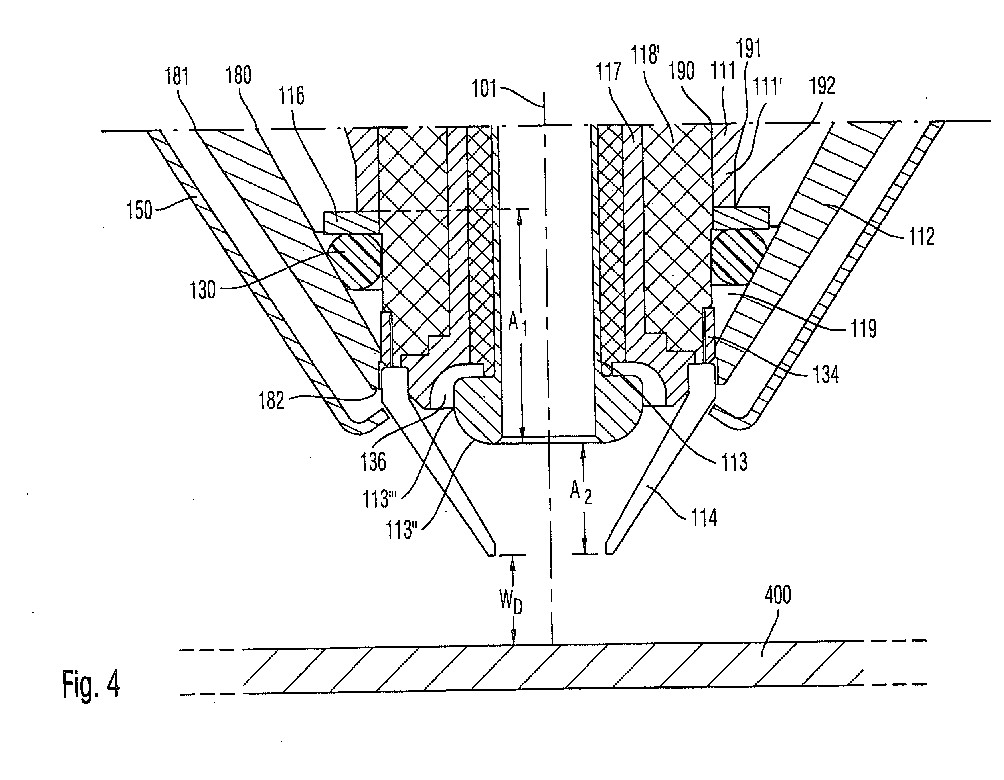
Eine Objektivlinse für ein Elektronenmikroskopiesystem umfasst eine rotationssymmetrische Polschuhanordnung zur Erzeugung eines fokussierenden Magnetfeldes mit einem inneren Polschuh (111) und einem äußeren Polschuh (112)mit einem in z-Richtung orientierten Spalt, einen Spulenkörper (115) und eine rotationssymmetrische Elektrodenanordnung zur Erzeugung eines fokussierenden elektrostatischen Feldes mit Strahlrohr (113) und einer mit Abstand von dem unteren Ende des Strahlrohrs angeordneten Abschlusselektrode (114); wobei der äußere Polschuh außen im Wesentlichen durch eine Konusfläche mit einem Konuswinkel α zur z-Richtung begrenzt ist, wobei die Abschlusselektrode außen im Wesentlichen durch eine Konusfläche mit einem Konuswinkel α' zur z-Richtung begrenzt ist, wobei die Abschlusselektrode zum Reduzieren des Magnetfelds in der Objektebene im Wesentlichen spaltfrei magnetisch an den äußeren Polschuh gekoppelt ist.
Applications Claiming Priority (2)
| Application Number | Priority Date | Filing Date | Title |
|---|---|---|---|
| DE10233002A DE10233002B4 (en) | 2002-07-19 | 2002-07-19 | Objective lens for an electron microscopy system and electron microscopy system |
| EP03016238A EP1385193B9 (en) | 2002-07-19 | 2003-07-17 | Objective lens for an electron microscopy system, and electron microscopy system |
Related Parent Applications (2)
| Application Number | Title | Priority Date | Filing Date |
|---|---|---|---|
| EP03016238A Division EP1385193B9 (en) | 2002-07-19 | 2003-07-17 | Objective lens for an electron microscopy system, and electron microscopy system |
| EP03016238.2 Division | 2003-07-17 |
Publications (2)
| Publication Number | Publication Date |
|---|---|
| EP2418673A2 EP2418673A2 (en) | 2012-02-15 |
| EP2418673A3 true EP2418673A3 (en) | 2014-08-20 |
Family
ID=29796478
Family Applications (2)
| Application Number | Title | Priority Date | Filing Date |
|---|---|---|---|
| EP03016238A Expired - Lifetime EP1385193B9 (en) | 2002-07-19 | 2003-07-17 | Objective lens for an electron microscopy system, and electron microscopy system |
| EP11008617.0A Withdrawn EP2418673A3 (en) | 2002-07-19 | 2003-07-17 | Lens for an electron microscope system and electron microscope system |
Family Applications Before (1)
| Application Number | Title | Priority Date | Filing Date |
|---|---|---|---|
| EP03016238A Expired - Lifetime EP1385193B9 (en) | 2002-07-19 | 2003-07-17 | Objective lens for an electron microscopy system, and electron microscopy system |
Country Status (4)
| Country | Link |
|---|---|
| US (1) | US6855938B2 (en) |
| EP (2) | EP1385193B9 (en) |
| JP (2) | JP4812238B2 (en) |
| DE (1) | DE10233002B4 (en) |
Families Citing this family (59)
| Publication number | Priority date | Publication date | Assignee | Title |
|---|---|---|---|---|
| EP1501115B1 (en) * | 2003-07-14 | 2009-07-01 | FEI Company | Dual beam system |
| EP1557867B1 (en) * | 2004-01-21 | 2008-02-27 | ICT Integrated Circuit Testing Gesellschaft für Halbleiterprüftechnik mbH | Focussing lens for charged particle beams |
| US7385197B2 (en) * | 2004-07-08 | 2008-06-10 | Ebara Corporation | Electron beam apparatus and a device manufacturing method using the same apparatus |
| US7312448B2 (en) * | 2005-04-06 | 2007-12-25 | Carl Zeiss Nts Gmbh | Method and apparatus for quantitative three-dimensional reconstruction in scanning electron microscopy |
| JP4588602B2 (en) * | 2005-09-30 | 2010-12-01 | 株式会社トプコン | Manufacturing method of electrostatic deflector |
| CN102103966B (en) * | 2005-11-28 | 2013-02-06 | 卡尔蔡司Smt有限责任公司 | Particle-optical component |
| US7825386B2 (en) * | 2006-10-25 | 2010-11-02 | Hermes-Microvision, Inc. | System and method for a charged particle beam |
| DE102006059162B4 (en) * | 2006-12-14 | 2009-07-09 | Carl Zeiss Nts Gmbh | Particle-optical arrangement |
| US7872236B2 (en) * | 2007-01-30 | 2011-01-18 | Hermes Microvision, Inc. | Charged particle detection devices |
| DE102007010873B4 (en) * | 2007-03-06 | 2009-07-30 | Carl Zeiss Nts Gmbh | objective lens |
| WO2009077450A2 (en) | 2007-12-17 | 2009-06-25 | Carl Zeiss Nts Gmbh | Scanning charged particle beams |
| DE102008009640A1 (en) * | 2008-02-18 | 2009-08-27 | Carl Zeiss Nts Gmbh | processing system |
| US20090246171A1 (en) * | 2008-03-27 | 2009-10-01 | Van Antwerp William P | Automatic system for dose control in treating hepatitis c using infusion pumps |
| JP2009266697A (en) * | 2008-04-25 | 2009-11-12 | National Institute Of Advanced Industrial & Technology | Cleaning device and cleaning method of vacuum device |
| DE102008025495A1 (en) * | 2008-05-28 | 2009-12-10 | Carl Zeiss Nts Gmbh | Electron microscopy system for examining surface of object, has voltage supply system configured to place electron beam source, radiant pipe and object in negative, positive and third potentials, respectively in operating mode |
| DE102008045336B4 (en) | 2008-09-01 | 2022-05-25 | Carl Zeiss Microscopy Gmbh | System for processing a sample with a laser beam and an electron beam or an ion beam |
| DE102009045008A1 (en) | 2008-10-15 | 2010-04-29 | Carl Zeiss Smt Ag | EUV lithography apparatus and method for processing a mask |
| US7960697B2 (en) | 2008-10-23 | 2011-06-14 | Hermes-Microvision, Inc. | Electron beam apparatus |
| US7919760B2 (en) * | 2008-12-09 | 2011-04-05 | Hermes-Microvision, Inc. | Operation stage for wafer edge inspection and review |
| US8094924B2 (en) * | 2008-12-15 | 2012-01-10 | Hermes-Microvision, Inc. | E-beam defect review system |
| DE102008064696B4 (en) | 2008-12-23 | 2022-01-27 | Carl Zeiss Microscopy Gmbh | Magnet array particle optical device and its use for imaging or illumination |
| DE102009008063A1 (en) * | 2009-02-09 | 2010-08-19 | Carl Zeiss Nts Gmbh | particle beam |
| JP5702552B2 (en) * | 2009-05-28 | 2015-04-15 | エフ イー アイ カンパニFei Company | Control method of dual beam system |
| DE102009033319B4 (en) | 2009-07-15 | 2019-02-21 | Carl Zeiss Microscopy Gmbh | Particle beam microscopy system and method of operating the same |
| DE102009036701A1 (en) | 2009-08-07 | 2011-03-03 | Carl Zeiss Nts Gmbh | Particle beam system and investigation method for this purpose |
| DE102010001346B4 (en) * | 2010-01-28 | 2014-05-08 | Carl Zeiss Microscopy Gmbh | Particle beam apparatus and method of operating a particle beam apparatus |
| DE102010008296A1 (en) | 2010-02-17 | 2011-08-18 | Carl Zeiss NTS GmbH, 73447 | Laser processing system, object holder and laser processing method |
| DE102010011898A1 (en) | 2010-03-18 | 2011-09-22 | Carl Zeiss Nts Gmbh | inspection system |
| US8735030B2 (en) | 2010-04-15 | 2014-05-27 | Carl Zeiss Smt Gmbh | Method and apparatus for modifying a substrate surface of a photolithographic mask |
| DE102010024625A1 (en) * | 2010-06-22 | 2011-12-22 | Carl Zeiss Nts Gmbh | Method for editing an object |
| DE102010064462B3 (en) | 2010-07-30 | 2024-07-11 | Carl Zeiss Microscopy Gmbh | TEM lamella |
| DE102010032894B4 (en) | 2010-07-30 | 2013-08-22 | Carl Zeiss Microscopy Gmbh | Tem lamella, process for its preparation and apparatus for carrying out the process |
| US8319192B2 (en) * | 2010-08-24 | 2012-11-27 | Hermes Microvision Inc. | Charged particle apparatus |
| JP5492032B2 (en) * | 2010-09-03 | 2014-05-14 | 日本電子株式会社 | Scanning electron microscope and method for switching use of objective lens of scanning electron microscope |
| DE102011109449B9 (en) * | 2011-08-04 | 2013-04-18 | Fraunhofer-Gesellschaft zur Förderung der angewandten Forschung e.V. | METHOD OF CALIBRATING A LASER SCANNER, USING THE METHOD AND MACHINING SYSTEM WITH A LASER SCANNER |
| TWI489222B (en) | 2012-02-16 | 2015-06-21 | 紐富來科技股份有限公司 | Electron beam rendering device and electron beam rendering method |
| JP6002428B2 (en) | 2012-04-24 | 2016-10-05 | 株式会社日立ハイテクノロジーズ | Charged particle beam equipment |
| US10586625B2 (en) | 2012-05-14 | 2020-03-10 | Asml Netherlands B.V. | Vacuum chamber arrangement for charged particle beam generator |
| EP2665082A1 (en) * | 2012-05-16 | 2013-11-20 | ICT Integrated Circuit Testing Gesellschaft für Halbleiterprüftechnik mbH | Element for fast magnetic beam deflection |
| JP2014041734A (en) | 2012-08-22 | 2014-03-06 | Hitachi High-Technologies Corp | Composite charged particle beam device |
| TWI617805B (en) * | 2012-09-14 | 2018-03-11 | Ebara Corp | Inspection device |
| DE102012020478A1 (en) | 2012-10-18 | 2014-05-08 | Carl Zeiss Microscopy Gmbh | Particle beam system and method for processing a TEM sample |
| US9057670B2 (en) * | 2013-05-30 | 2015-06-16 | International Business Machines Corporation | Transmission electron microscope sample fabrication |
| NL2013814B1 (en) | 2013-11-14 | 2016-05-10 | Mapper Lithography Ip Bv | Multi-electrode vacuum arrangement. |
| TWI502616B (en) * | 2014-08-08 | 2015-10-01 | Nat Univ Tsing Hua | Desktop electron microscope and wide range tunable magnetic lens thereof |
| JP6177817B2 (en) * | 2015-01-30 | 2017-08-09 | 松定プレシジョン株式会社 | Charged particle beam apparatus and scanning electron microscope |
| JP6404736B2 (en) * | 2015-02-06 | 2018-10-17 | 株式会社日立ハイテクノロジーズ | Compound charged particle beam system |
| CN108292580B (en) | 2015-12-03 | 2019-06-11 | 松定精度株式会社 | Charged particle beam device and scanning electron microscope |
| DE102016002883B4 (en) | 2016-03-09 | 2023-05-17 | Carl Zeiss Microscopy Gmbh | Method for structuring an object and particle beam system therefor |
| US10777382B2 (en) | 2017-11-21 | 2020-09-15 | Focus-Ebeam Technology (Beijing) Co., Ltd. | Low voltage scanning electron microscope and method for specimen observation |
| US11264198B2 (en) * | 2018-10-15 | 2022-03-01 | Applied Materials Israel Ltd. | Objective lens arrangement |
| CN114171361B (en) * | 2020-09-11 | 2024-09-06 | 聚束科技(北京)有限公司 | An electron microscope |
| CN114220725B (en) | 2020-12-02 | 2024-05-07 | 聚束科技(北京)有限公司 | Electron microscope |
| CN114256043B (en) | 2020-12-02 | 2024-04-05 | 聚束科技(北京)有限公司 | An electron beam system |
| US11640896B2 (en) * | 2021-05-13 | 2023-05-02 | Nuflare Technology, Inc. | Method and apparatus for Schottky TFE inspection |
| CN115497791B (en) * | 2022-09-14 | 2024-12-17 | 国仪量子技术(合肥)股份有限公司 | Scanning electron microscope objective |
| CN115527823A (en) * | 2022-10-31 | 2022-12-27 | 中国科学院电工研究所 | A kind of objective lens and environmental scanning electron microscope |
| US20250239431A1 (en) * | 2024-01-24 | 2025-07-24 | Taiwan Semiconductor Manufacturing Company, Ltd. | Electron microscope detector and related methods |
| CN118588520B (en) * | 2024-08-06 | 2024-10-18 | 北京惠然肯来科技中心(有限合伙) | Magnetic objective lens structure for particle beam control device and particle beam control device |
Citations (8)
| Publication number | Priority date | Publication date | Assignee | Title |
|---|---|---|---|---|
| EP0180723A1 (en) * | 1984-08-13 | 1986-05-14 | ICT Integrated Circuit Testing Gesellschaft für Halbleiterprüftechnik mbH | Corpuscular beam device |
| EP0274622A1 (en) * | 1986-12-12 | 1988-07-20 | ICT Integrated Circuit Testing Gesellschaft für Halbleiterprüftechnik mbH | Detector assembly with detector objective for corpuscular ray instruments |
| EP0333018A2 (en) * | 1988-03-17 | 1989-09-20 | ICT Integrated Circuit Testing Gesellschaft für Halbleiterprüftechnik mbH | Objective lens for focusing charged particles |
| EP0461442A2 (en) * | 1990-06-11 | 1991-12-18 | ICT Integrated Circuit Testing Gesellschaft für HalbleiterprÀ¼ftechnik mbH | Particle beam apparatus |
| US5093572A (en) * | 1989-11-02 | 1992-03-03 | Mitsubishi Denki Kabushiki Kaisha | Scanning electron microscope for observation of cross section and method of observing cross section employing the same |
| EP0893816A2 (en) * | 1997-07-25 | 1999-01-27 | LEO Elektronenmikroskopie GmbH | Corpuscular beam apparatus |
| EP0910108A1 (en) * | 1997-09-29 | 1999-04-21 | Advantest Corporation | Electron beam lens |
| DE19845329A1 (en) * | 1998-03-10 | 1999-09-23 | Erik Essers | Scanning electron microscope for acquiring images of specimens in high pressure chamber |
Family Cites Families (20)
| Publication number | Priority date | Publication date | Assignee | Title |
|---|---|---|---|---|
| DE2922325A1 (en) * | 1979-06-01 | 1980-12-11 | Philips Patentverwaltung | GRID ELECTRON MICROSCOPE |
| SU997135A1 (en) | 1981-07-13 | 1983-02-15 | Предприятие П/Я А-7638 | Optronic system for microprobe device |
| JPS6074250A (en) * | 1983-09-29 | 1985-04-26 | Jeol Ltd | Magnetic field type lens |
| GB8401578D0 (en) * | 1984-01-19 | 1984-02-22 | Cleaver J R A | Ion and electron beam electrostatic and magnetic lens systems |
| JPH0636346B2 (en) * | 1988-03-09 | 1994-05-11 | セイコー電子工業株式会社 | Charged particle beam apparatus and sample observation method using the same |
| JPH0864163A (en) * | 1994-08-19 | 1996-03-08 | Jeol Ltd | Charged particle beam device |
| US5623183A (en) * | 1995-03-22 | 1997-04-22 | Litton Systems, Inc. | Diverging beam electron gun for a toxic remediation device with a dome-shaped focusing electrode |
| US5731586A (en) * | 1995-05-25 | 1998-03-24 | Jeol Ltd. | Magnetic-electrostatic compound objective lens |
| JP3372138B2 (en) * | 1995-06-26 | 2003-01-27 | 株式会社日立製作所 | Scanning electron microscope |
| JPH10106466A (en) * | 1996-09-30 | 1998-04-24 | Eiko Eng:Kk | Magnetic field type objective electron lens |
| JP3457875B2 (en) * | 1998-01-27 | 2003-10-20 | 日本電子株式会社 | Method for observing sample cross section in FIB-SEM apparatus and FIB-SEM apparatus |
| JP2002507045A (en) * | 1998-03-10 | 2002-03-05 | エッサーズ、エリック | Scanning electron microscope |
| JP3117950B2 (en) * | 1998-05-21 | 2000-12-18 | セイコーインスツルメンツ株式会社 | Charged particle device |
| EP0969493A1 (en) * | 1998-07-03 | 2000-01-05 | ICT Integrated Circuit Testing Gesellschaft für Halbleiterprüftechnik mbH | Apparatus and method for examining specimen with a charged particle beam |
| EP1022766B1 (en) * | 1998-11-30 | 2004-02-04 | Advantest Corporation | Particle beam apparatus |
| JP4162343B2 (en) * | 1999-12-24 | 2008-10-08 | エスアイアイ・ナノテクノロジー株式会社 | Electron beam equipment |
| JP2002056794A (en) * | 2000-08-08 | 2002-02-22 | National Institute For Materials Science | Objective lens for electron microscope |
| JP2002134051A (en) * | 2000-10-20 | 2002-05-10 | Seiko Instruments Inc | Electromagnetic field superimposed lens and electron beam device using the same |
| JP4178741B2 (en) * | 2000-11-02 | 2008-11-12 | 株式会社日立製作所 | Charged particle beam apparatus and sample preparation apparatus |
| JP4215454B2 (en) * | 2001-07-12 | 2009-01-28 | 株式会社日立製作所 | Sample unevenness determination method and charged particle beam apparatus |
-
2002
- 2002-07-19 DE DE10233002A patent/DE10233002B4/en not_active Expired - Fee Related
-
2003
- 2003-07-16 US US10/619,475 patent/US6855938B2/en not_active Expired - Lifetime
- 2003-07-17 EP EP03016238A patent/EP1385193B9/en not_active Expired - Lifetime
- 2003-07-17 EP EP11008617.0A patent/EP2418673A3/en not_active Withdrawn
- 2003-07-18 JP JP2003277006A patent/JP4812238B2/en not_active Expired - Lifetime
-
2011
- 2011-06-14 JP JP2011132388A patent/JP5395118B2/en not_active Expired - Lifetime
Patent Citations (8)
| Publication number | Priority date | Publication date | Assignee | Title |
|---|---|---|---|---|
| EP0180723A1 (en) * | 1984-08-13 | 1986-05-14 | ICT Integrated Circuit Testing Gesellschaft für Halbleiterprüftechnik mbH | Corpuscular beam device |
| EP0274622A1 (en) * | 1986-12-12 | 1988-07-20 | ICT Integrated Circuit Testing Gesellschaft für Halbleiterprüftechnik mbH | Detector assembly with detector objective for corpuscular ray instruments |
| EP0333018A2 (en) * | 1988-03-17 | 1989-09-20 | ICT Integrated Circuit Testing Gesellschaft für Halbleiterprüftechnik mbH | Objective lens for focusing charged particles |
| US5093572A (en) * | 1989-11-02 | 1992-03-03 | Mitsubishi Denki Kabushiki Kaisha | Scanning electron microscope for observation of cross section and method of observing cross section employing the same |
| EP0461442A2 (en) * | 1990-06-11 | 1991-12-18 | ICT Integrated Circuit Testing Gesellschaft für HalbleiterprÀ¼ftechnik mbH | Particle beam apparatus |
| EP0893816A2 (en) * | 1997-07-25 | 1999-01-27 | LEO Elektronenmikroskopie GmbH | Corpuscular beam apparatus |
| EP0910108A1 (en) * | 1997-09-29 | 1999-04-21 | Advantest Corporation | Electron beam lens |
| DE19845329A1 (en) * | 1998-03-10 | 1999-09-23 | Erik Essers | Scanning electron microscope for acquiring images of specimens in high pressure chamber |
Non-Patent Citations (5)
| Title |
|---|
| DE JAGER P W H ET AL: "A combined objective lens for electrons and ions", MICROELECTRONIC ENGINEERING, ELSEVIER PUBLISHERS BV., AMSTERDAM, NL, vol. 30, no. 1-4, 1 January 1996 (1996-01-01), pages 427 - 430, XP004597546, ISSN: 0167-9317 * |
| FROSIEN J ET AL: "COMPOUND MAGNETIC AND ELECTROSTATIC LENSES FOR LOW-VOLTAGE APPLICATIONS", JOURNAL OF VACUUM SCIENCE AND TECHNOLOGY: PART B, AVS / AIP, MELVILLE, NEW YORK, NY, US, vol. 7, no. 6, 1 November 1989 (1989-11-01), pages 1874 - 1877, XP000117179, ISSN: 1071-1023 * |
| FROSIEN J ET AL: "High performance electron optical column for testing ICs with submicrometer design rules", MICROELECTRONIC ENGINEERING, ELSEVIER PUBLISHERS BV., AMSTERDAM, NL, vol. 7, no. 2-4, 1 January 1987 (1987-01-01), pages 163 - 172, XP025931934, ISSN: 0167-9317, [retrieved on 19870101] * |
| KOLARIK V ET AL: "A design of a new axially symmetric secondary electron detector for the transmission electron microscope", MEASUREMENT SCIENCE AND TECHNOLOGY, IOP, BRISTOL, GB, vol. 1, no. 5, 1 May 1990 (1990-05-01), pages 391 - 395, XP020066215, ISSN: 0957-0233 * |
| REIMER, LUDWIG: "Scanning Electron Microscopy", 1986, SPRINGER, BERLIN HEIDELBERG NEW YORK TOKYO, XP002493854 * |
Also Published As
| Publication number | Publication date |
|---|---|
| EP2418673A2 (en) | 2012-02-15 |
| EP1385193B1 (en) | 2012-05-02 |
| DE10233002B4 (en) | 2006-05-04 |
| US20040084629A1 (en) | 2004-05-06 |
| JP4812238B2 (en) | 2011-11-09 |
| JP2004134379A (en) | 2004-04-30 |
| EP1385193B9 (en) | 2012-08-08 |
| JP5395118B2 (en) | 2014-01-22 |
| EP1385193A3 (en) | 2009-12-16 |
| EP1385193A2 (en) | 2004-01-28 |
| JP2011222525A (en) | 2011-11-04 |
| DE10233002A1 (en) | 2004-02-12 |
| US6855938B2 (en) | 2005-02-15 |
Similar Documents
| Publication | Publication Date | Title |
|---|---|---|
| EP2418673A3 (en) | Lens for an electron microscope system and electron microscope system | |
| Farahani et al. | Single quantum dot coupled to a scanning optical antenna: a tunable superemitter | |
| EP2446246B1 (en) | Device and method for selecting particles | |
| EP0218829B1 (en) | Arrangement for the detection of secondary and/or back-scattering electrons in an electron beam apparatus | |
| ATE505808T1 (en) | METHOD FOR OBTAINING A SCANNING TRANSMISSION IMAGE OF A SAMPLE IN A PARTICLE OPTICAL DEVICE | |
| JPWO2000019482A1 (en) | scanning electron microscope | |
| DE102007010873B4 (en) | objective lens | |
| EP1197985A3 (en) | Scanning charged-particle microscope | |
| JP6722958B1 (en) | Electron beam applying apparatus and electron beam emitting method in electron beam applying apparatus | |
| EP2804199A3 (en) | Scanning charged particle microscope, image acquisition method, and electron detection method | |
| EP3742470A3 (en) | Multi-beam scanning electron microscope | |
| CN110596877B (en) | An optical zoom microscope with continuously adjustable objective and eyepiece focal lengths | |
| CN210403653U (en) | Scanning electron microscope in non-magnetic environment | |
| AT137611B (en) | Device for imaging objects. | |
| DE102023101628B4 (en) | Particle beam microscope | |
| DE19915572A1 (en) | Immersion lens for electron beam projection system | |
| WO2023186558A1 (en) | Illumination for a microscope, microscope having dark-field illumination, use for examining blood, and method for illuminating a sample | |
| DE102024002911B4 (en) | Electron beam microscope and method for operating it | |
| DE102022113918A1 (en) | Method for imaging, processing and/or analyzing an object using a particle beam device, computer program product and particle beam device for carrying out the method | |
| DE102006040057A1 (en) | Device for concentration of polarized light of area substantially smaller than light wave length, has slots to support excitation of automatic concentrated surface plasmon resonance in metal shield by light radiation in chamber | |
| DE102011111546A1 (en) | Interchangeable alignment marking unit | |
| JP2002540562A (en) | Magnetic immersion lens | |
| DE10347969B4 (en) | Method for precise positioning of individual particles in or on a substrate surface and application of a device suitable for this purpose | |
| DE102024119459B3 (en) | Beam generating device for a multi-particle beam system and multi-particle beam system | |
| US20040084620A1 (en) | Lens for a scanning electron microscope |
Legal Events
| Date | Code | Title | Description |
|---|---|---|---|
| AC | Divisional application: reference to earlier application |
Ref document number: 1385193 Country of ref document: EP Kind code of ref document: P |
|
| AK | Designated contracting states |
Kind code of ref document: A2 Designated state(s): CZ DE GB NL |
|
| PUAI | Public reference made under article 153(3) epc to a published international application that has entered the european phase |
Free format text: ORIGINAL CODE: 0009012 |
|
| PUAL | Search report despatched |
Free format text: ORIGINAL CODE: 0009013 |
|
| AK | Designated contracting states |
Kind code of ref document: A3 Designated state(s): CZ DE GB NL |
|
| RIC1 | Information provided on ipc code assigned before grant |
Ipc: H01J 37/30 20060101ALI20140716BHEP Ipc: H01J 37/145 20060101AFI20140716BHEP |
|
| STAA | Information on the status of an ep patent application or granted ep patent |
Free format text: STATUS: THE APPLICATION IS DEEMED TO BE WITHDRAWN |
|
| 18D | Application deemed to be withdrawn |
Effective date: 20150221 |