EP0333018A2 - Objective lens for focusing charged particles - Google Patents
Objective lens for focusing charged particles Download PDFInfo
- Publication number
- EP0333018A2 EP0333018A2 EP89104133A EP89104133A EP0333018A2 EP 0333018 A2 EP0333018 A2 EP 0333018A2 EP 89104133 A EP89104133 A EP 89104133A EP 89104133 A EP89104133 A EP 89104133A EP 0333018 A2 EP0333018 A2 EP 0333018A2
- Authority
- EP
- European Patent Office
- Prior art keywords
- electrode
- lens
- objective lens
- magnetic
- sample
- Prior art date
- Legal status (The legal status is an assumption and is not a legal conclusion. Google has not performed a legal analysis and makes no representation as to the accuracy of the status listed.)
- Granted
Links
- 239000002245 particle Substances 0.000 title claims description 5
- 238000007654 immersion Methods 0.000 claims abstract description 17
- 239000011163 secondary particle Substances 0.000 claims 2
- 230000005684 electric field Effects 0.000 abstract description 2
- 239000000523 sample Substances 0.000 description 14
- 230000000694 effects Effects 0.000 description 6
- 230000001133 acceleration Effects 0.000 description 4
- 230000004075 alteration Effects 0.000 description 3
- 230000008859 change Effects 0.000 description 3
- 238000003384 imaging method Methods 0.000 description 3
- 230000007935 neutral effect Effects 0.000 description 3
- 230000009467 reduction Effects 0.000 description 3
- 230000001960 triggered effect Effects 0.000 description 3
- 230000008901 benefit Effects 0.000 description 2
- 238000011161 development Methods 0.000 description 2
- 230000018109 developmental process Effects 0.000 description 2
- 238000010894 electron beam technology Methods 0.000 description 2
- 230000006872 improvement Effects 0.000 description 2
- 230000033228 biological regulation Effects 0.000 description 1
- 230000007423 decrease Effects 0.000 description 1
- 230000001419 dependent effect Effects 0.000 description 1
- 230000002349 favourable effect Effects 0.000 description 1
- 239000012212 insulator Substances 0.000 description 1
- 230000003993 interaction Effects 0.000 description 1
- 238000004519 manufacturing process Methods 0.000 description 1
- 239000000463 material Substances 0.000 description 1
- 238000005259 measurement Methods 0.000 description 1
- 238000004377 microelectronic Methods 0.000 description 1
- 230000005693 optoelectronics Effects 0.000 description 1
- 239000004065 semiconductor Substances 0.000 description 1
- 238000012876 topography Methods 0.000 description 1
Images

Classifications
-
- H—ELECTRICITY
- H01—ELECTRIC ELEMENTS
- H01J—ELECTRIC DISCHARGE TUBES OR DISCHARGE LAMPS
- H01J37/00—Discharge tubes with provision for introducing objects or material to be exposed to the discharge, e.g. for the purpose of examination or processing thereof
- H01J37/02—Details
- H01J37/04—Arrangements of electrodes and associated parts for generating or controlling the discharge, e.g. electron-optical arrangement or ion-optical arrangement
- H01J37/10—Lenses
- H01J37/145—Combinations of electrostatic and magnetic lenses
Definitions
- the invention relates to an objective lens for focusing charged particles.
- the invention has for its object to provide an objective lens of the type mentioned, with which a charge-neutral examination of poorly conductive samples is guaranteed. This object is achieved by an objective lens according to claim 1.
- the advantage that can be achieved with the invention is, in particular, that non-conductive or poorly conductive samples can be imaged and measured with high resolution and with no charge.
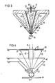
- 1 to 4 show exemplary embodiments of objective lenses according to the invention for scanning electron microscopes.
- the objective lens shown schematically in FIG. 1 forms the component of a scanning electron microscope with which an electron source or its intermediate image reduced by condenser lenses is imaged on the sample PR, in particular an opto or microelectronic component.
- the objective lens consists of an asymmetrical magnetic lens ML, an electrostatic immersion lens OE / UE superimposed on the magnetic lens ML, a control electrode ST which is at an adjustable potential and a detector DT for detecting the secondary and backscattered electrons SE triggered by the primary electrons PE at the respective measuring point.
- the immersion lens comprises a conical electrode OE, which is insulated in the area of the upper pole shoe OP of the magnetic lens ML, and a tubular electrode UE which projects into the bore of the lower pole shoe UP and whose potentials U OE or U UE are selected such that they are within the objective lens decelerating the primary electrons PE or building up an electric field accelerating the secondary electrons SE.
- the color and aperture error constants of the magnetic lens ML exceed those of the electrostatic-magnetic objective lens by almost an order of magnitude if the primary electrons PE are braked by a factor of 10 in the field of the immersion lens.
- the detector DT for detecting the secondary and backscattered electrons SE triggered at the respective measuring point and accelerated in the field of the immersion lens is located in the exemplary embodiment shown directly above the magnetic lens ML arranges. It consists of a ring-shaped electron-sensitive part ES and a hollow cylinder RE which is insulated in its central bore.
- U ES 10 kV
- the hollow cylinder RE which has a positive potential U RE of, for example, U OE - 1 kV ⁇ U RE ⁇ U OE, should reach into the upper one Reach in the pole shoe hole of the ML magnetic lens.
- detectors DT semiconductor detectors, channel plates or scintillator-light guide combinations come into consideration as detectors DT, which, in contrast to FIG. 1, can also be arranged within the objective lens.
- ring-shaped detectors DT have the advantage that almost all of the secondary electrons SE extracted from the sample PR in the field of the immersion lens can be detected.
- Quadrant detectors can of course also be used.
- i PR denotes the sample current, i PE the primary electron current, i RE the backscattered electron current and i SE the secondary electron current.
- Such a scanning electron microscope equipped with the objective lens according to the invention does not require such a change in the beam energy E PE with the associated disadvantages (change in the acceleration voltage, refocusing of the primary electron beam, readjustment of the stigmator field), since the intensity of the secondary electron current i SE can be determined using the electrode arranged below the magnetic lens ML ST (regulation of the strength of the suction field acting on the secondary electrons SE) can weaken or increase to the required extent.
- the resolution at low acceleration voltages below about 5 kV (the neutral point energies are, with a few exceptions, in the energy range between about 0.5 and 4 keV) is essentially limited by the Boersch effect and the color error of the objective lens.
- the Coulomb repulsion of the electrons their spatial distance and thus the beam diameter on the sample increases (lateral Boersch effect).
- the electron-electron interaction in areas of high current densities, in particular in the beam generator and in the beam crossing points leads to a broadening of the energy distribution of the primary electrons (energetic Boersch effect), which has an unfavorable effect on the probe diameter via the chromatic aberration of the objective lens .
- the objective lens according to the invention which replaces the conventional objective lens of the scanning electron microscope with its comparatively large aberration, is preferably used as a device for braking and focusing the primary electrons.
- the improvement in the imaging properties results from the reduction in the color and aperture error constants associated with the deceleration of the primary electrons PE, but also from the shift of the main plane of the lens ML in the direction of the sample PR (reduction of the focal length f), which in turn has a favorable effect on that of the focal length f proportional color error constant C F affects.
- the electrode ST for setting the strength of the suction field acting on the secondary electrons SE is likewise arranged directly below the magnetic lens ML and is preferably frustoconical.
- the electrode ST can also be integrated into the lower pole shoe UP of the magnetic lens ML by applying the desired potential U ST to the lower part UP1, which is separated from the upper pole shoe part by an insulator IS.
- FIG. 4 shows an electrostatic objective lens (immersion lens with central electrode) whose source-side electrode OE has an annular part RB which acts as an aperture and a hollow cylinder HZ which extends in the direction of the sample PR.
- the center electrode ME which is at a variable positive potential U ME
- the sample-side electrode UE and the electrode ST for controlling the intensity of the secondary electron current emanating from the sample PR are each frustoconical in the exemplary embodiment and arranged concentrically to the axis OA of the hollow cylinder HZ.
- the side faces of the conical electrodes ME, UE or ST should preferably form an angle ⁇ 'between about 30 and 70 ° with the axis OA.
- the detector DT for detecting the secondary electrons SE triggered on the sample PR is arranged within the objective lens between the source-side and the middle electrode OE or ME. It consists of a ring-shaped electron sensitive Part that is preferably segmented. Since the hollow cylinder HZ is at a somewhat lower potential U HZ than the center electrode ME (U HZ ⁇ U ME ), the secondary electrons SE emitted in the direction of the beam axis OA are also deflected and detected towards the detector DT.
- This lens can also preferably be used as a lens in a high-resolution scanning electron microscope in order to brake the primary electrons PE accelerated to high kinetic energies to the desired final energy.
- the electrode OE is then subjected to the potential of the anode of the beam generator, for example, while the electrode UE is at the potential of the sample PR, that is to say usually at ground.
- the invention is of course not limited to the exemplary embodiments described. So it is easily possible to replace the conical electrode OE with a tubular electrode. However, it is important to ensure that the tube diameter is larger than the maximum cross section of the diverging secondary electron beam generated within the objective lens.
- the lower pole piece can also serve as the second electrode of the immersion lens.
- a significant improvement in the resolution of a scanning electron microscope can be expected in particular if the energy of the primary electrons is reduced by at least a factor of two using the objective lens according to the invention.
Landscapes
- Chemical & Material Sciences (AREA)
- Analytical Chemistry (AREA)
- Analysing Materials By The Use Of Radiation (AREA)
Abstract
Die erfindungsgemäße Objektivlinse bildet die Komponente eines Rasterelektronenmikroskops, mit der man die Elektronenquelle oder deren durch Kondensorlinsen verkleinertes Zwischenbild auf eine Probe (PR) abbildet. Sie besteht aus einer unsymmetrischen Magnetlinse (ML), einer der Magnetlinse (ML) überlagerten elektrostatischen Immersionslinse (OE/UE), einer auf einem einstellbaren Potential (UST) liegenden Elektrode (ST) zur Steuerung der Intenstiät des von der Probe (PR) ausgehenden Stroms der sekundären und rückgestreuten Elektronen (SE) und einem unmittelbar oberhalb der Magnetlinse (ML) angeordneten Detektor (DT). Die Elektroden (OE, UE) der Immersionslinse sind mit Potentialen derart beaufschlagt, daß sich innerhalb der Objektivlinse ein die Primärelektronen (PE) abbremsendes elektrisches Feld aufbaut. 
Description
Die Erfindung bezieht sich auf eine Objektivlinse zur Fokussierung geladener Teilchen.The invention relates to an objective lens for focusing charged particles.
In allen Bereichen der Entwicklung und Fertigung mikro- und optoelektronischer Bauelemente besteht ein steigender Bedarf an hochauflösenden Rasterelektronenmikroskopen, um Submikrometerstrukturen visuell beurteilen, Abweichungen von Sollmustern feststellen und topographische Daten wie Höhen, Breiten oder Neigungswinkel erfassen und auswerten zu können. Konventionelle Rasterelektronenmikroskope erreichen die geforderte Auflösung von wenigen Nanometern allerdings erst bei hohen Beschleunigungsspannungen oberhalb etwa 20 kV, wo Resiststrukturen und integrierte Schaltungen geschädigt und nicht- oder schlechtleitende Proben aufgeladen werden.In all areas of the development and production of micro and optoelectronic components, there is an increasing need for high-resolution scanning electron microscopes to visually assess sub-micrometer structures, determine deviations from target patterns and to be able to record and evaluate topographic data such as heights, widths or inclination angles. Conventional scanning electron microscopes only achieve the required resolution of a few nanometers at high acceleration voltages above about 20 kV, where resist structures and integrated circuits are damaged and non- or poorly conductive samples are charged.
Der Erfindung liegt die Aufgabe zugrunde, eine Objektivlinse der eingangs genannten Art anzugeben, mit der eine aufladungsneutrale Untersuchung schlechtleitender Proben gewährleistet ist. Diese Aufgabe wird erfindungsgemäß durch eine Objektivlinse nach Patentanspruch 1 gelöst.The invention has for its object to provide an objective lens of the type mentioned, with which a charge-neutral examination of poorly conductive samples is guaranteed. This object is achieved by an objective lens according to claim 1.
Der mit der Erfindung erzielbare Vorteil besteht insbesondere darin, daß nicht- oder schlechtleitende Proben mit hoher Auflösung und aufladungsneutral abgebildet und vermessen werden können.The advantage that can be achieved with the invention is, in particular, that non-conductive or poorly conductive samples can be imaged and measured with high resolution and with no charge.
Die Ansprüche 2 bis 8 sind auf bevorzugte Ausgestaltungen und Weiterbildungen der im folgenden anhand der Zeichnung näher erläuterten Erfindung gerichtet.Claims 2 to 8 are directed to preferred refinements and developments of the invention explained in more detail below with reference to the drawing.
Hierbei zeigen die FIG 1 bis 4 Ausführungsbeispiele erfindungsgemäßer Objektivlinsen für Rasterelektronenmikroskope.1 to 4 show exemplary embodiments of objective lenses according to the invention for scanning electron microscopes.
Die in FIG 1 schematisch dargestellte Objektivlinse bildet die Komponente eines Rasterelektronenmikroskops, mit der man eine Elektronenquelle oder deren durch Kondensorlinsen verkleinertes Zwischenbild auf die Probe PR, insbesondere ein opto- oder mikroelektronisches Bauelement, abbildet. Die Objektivlinse besteht aus einer unsymmetrischen Magnetlinse ML, einer der Magnetlinse ML überlagerten elektrostatischen Immersionslinse OE/UE, einer auf einem einstellbaren Potential liegenden Steuerelektrode ST und einem Detektor DT zum Nachweis der von den Primärelektronen PE an der jeweiligen Meßstelle ausgelösten sekundären und rückgestreuten Elektronen SE. Die Immersionslinse umfaßt eine im Bereich des oberen Polschuhs OP der Magnetlinse ML isoliert angeordnete, kegelförmige Elektrode OE und eine in die Bohrung des unteren Polschuhes UP hineinragende Rohrelektrode UE, deren Potentiale UOE bzw. UUE so gewählt sind, daß sich innerhalb der Objektivlinse ein die Primärelektronen PE abbrem sendes bzw. ein die Sekundärelektronen SE beschleunigendes elektrisches Feld aufbaut. So werden die mit einer hohen kinetischen Energie von beispielsweise EPE = 10 keV in die Linse eintretenden Primärelektronen PE bei einem Kathodenpotential von UK = - 1 kV und einem Anodenpotential von UA = + 9 kV auf die Endenergie von beispielsweise EPE = 1 keV abgebremst, wenn man die quellenseitige Elektrode OE der Immersionslinse auf das Anodenpotential UOE = UA = + 9 kV und die Elektrode UE auf Masse UUE = 0 V legt.The objective lens shown schematically in FIG. 1 forms the component of a scanning electron microscope with which an electron source or its intermediate image reduced by condenser lenses is imaged on the sample PR, in particular an opto or microelectronic component. The objective lens consists of an asymmetrical magnetic lens ML, an electrostatic immersion lens OE / UE superimposed on the magnetic lens ML, a control electrode ST which is at an adjustable potential and a detector DT for detecting the secondary and backscattered electrons SE triggered by the primary electrons PE at the respective measuring point. The immersion lens comprises a conical electrode OE, which is insulated in the area of the upper pole shoe OP of the magnetic lens ML, and a tubular electrode UE which projects into the bore of the lower pole shoe UP and whose potentials U OE or U UE are selected such that they are within the objective lens decelerating the primary electrons PE or building up an electric field accelerating the secondary electrons SE. Thus, the primary electrons PE entering the lens with a high kinetic energy of, for example, E PE = 10 keV, have a cathode potential of U K = - 1 kV and an anode potential of U A = + 9 kV on the final energy of, for example, E PE = 1 keV braked if you place the source-side electrode OE of the immersion lens on the anode potential U OE = U A = + 9 kV and the electrode UE on ground U UE = 0 V.
Aufgrund des dem fokussierenden Magnetfeld überlagerten elektrischen Verzögerungsfeldes besitzt die erfindungsgemäße Objektivlinse erheblich bessere Abbildungseigenschaften als die magnetische Linse ML (UOE = OV). So übertreffen die Farb- und Öffnungsfehlerkonstanten der magnetischen Linse ML die der elektrostatisch-magnetischen Objektivlinse um annähernd eine Größenordnung, wenn man die Primärelektronen PE im Feld der Immersionslinse um etwa einen Faktor 10 abbremst.Because of the electrical delay field superimposed on the focusing magnetic field, the objective lens according to the invention has considerably better imaging properties than the magnetic lens ML (U OE = OV). The color and aperture error constants of the magnetic lens ML exceed those of the electrostatic-magnetic objective lens by almost an order of magnitude if the primary electrons PE are braked by a factor of 10 in the field of the immersion lens.
Der Detektor DT zum Nachweis der am jeweiligen Meßpunkt ausgelösten und im Feld der Immersionslinse beschleunigten sekundären und rückgestreuten Elektronen SE ist in dem gezeigten Ausführungsbeispiel unmittelbar oberhalb der Magnetlinse ML ange ordnet. Er besteht aus einem ringförmigen elektronensensitiven Teil ES und einer in dessen Zentralbohrung isoliert gehalterten Hohlzylinder RE. Um die Primärelektronen PE gegenüber der üblicherweise am ringförmigen Teil ES anliegenden Hochspannung von beispielsweise UES = 10 kV abzuschirmen, sollte der mit einem positiven Potential URE von beispielsweise UOE- 1 kV≾URE≾ UOE beaufschlagte Hohlzylinder RE bis in die obere Polschuhbohrung der Magnetlinse ML hineinreichen. Als Detektoren DT kommen insbesondere Halbleiterdetektoren, Channel-Plates oder Szintillator-Lichtleiter-Kombinationen in Betracht, die, im Unterschied zu FIG 1, auch innerhalb der Objektivlinse angeordnet sein können. Hierbei besitzen ringförmige Detektoren DT den Vorteil, daß sich nahezu alle der im Feld der Immersionslinse von der Probe PR abgesaugten Sekundärelektronen SE nachweisen lassen. Es können selbstverständlich auch Quadrantendetektoren verwendet werden.The detector DT for detecting the secondary and backscattered electrons SE triggered at the respective measuring point and accelerated in the field of the immersion lens is located in the exemplary embodiment shown directly above the magnetic lens ML arranges. It consists of a ring-shaped electron-sensitive part ES and a hollow cylinder RE which is insulated in its central bore. In order to shield the primary electrons PE from the high voltage of U ES = 10 kV, for example, which is usually present on the ring-shaped part ES, the hollow cylinder RE, which has a positive potential U RE of, for example, U OE - 1 kV≾U RE ≾ U OE, should reach into the upper one Reach in the pole shoe hole of the ML magnetic lens. In particular, semiconductor detectors, channel plates or scintillator-light guide combinations come into consideration as detectors DT, which, in contrast to FIG. 1, can also be arranged within the objective lens. Here, ring-shaped detectors DT have the advantage that almost all of the secondary electrons SE extracted from the sample PR in the field of the immersion lens can be detected. Quadrant detectors can of course also be used.
In einem Rasterelektronenmikroskop ist eine aufladungsneutrale Vermessung und Abbildung isolierender Proben nur dann gewährleistet, wenn der jeweiligen Meßstelle keine Ladungen zugeführt oder entzogen werden. Man ist deshalb bestrebt die Bedingung
iPR = iPE - (iRE + iSE) : = 0
zumindest näherungsweise zu erfüllen. In dieser Gleichung bezeichnet iPR den Probenstrom, iPE den Primärelektronenstrom, iRE den Strom der rückgestreuten Elektronen und iSE den Sekundärelektronenstrom. Da der Sekundärelektronenstrom iSE gemäß der Gleichung
iSE = σ (EPE) · iPE
vom Primärelektronenstrom iPE und der von der Primärelektronenenergie EPE abhängigen Größe σ ( σ wird üblicherweise als Ausbeute emittierter Elektronen bezeichnet) bestimmt wird, versucht man in konventionellen Rasterelektronenmikriskopen, die Ladungsbilanz durch eine Anpassung der Strahlenergie EPE (Änderung von iSE ∼ σ (EPE)) an die jeweiligen Gegebenheiten (Material der Meßstelle usw.) auszugleichen. Bei einem mit einer er findungsgemäßen Objektivlinse ausgestatteten Rasterelektronenmikroskop ist eine solche Änderung der Strahlenergie EPE mit den damit verbundenen Nachteilen (Änderung der Beschleunigungsspannung, Nachfokussierung des Primärelektronenstrahls, Neueinstellung des Stigmatorfeldes) nicht notwendig, da man die Intensität des Sekundärelektronenstromes iSE mit Hilfe der unterhalb der Magnetlinse ML angeordneten Elektrode ST (Regelung der Stärke des auf die Sekundärelektronen SE wirkenden Absaugfeldes) in dem erforderlichen Maß abschwächen oder erhöhen kann. Das Potential UST der die Absaugfeldstärke definierenden Ringelektrode bzw. Blende ST muß hierbei nur innerhalb eines Bereichs von etwa - 100 Volt ≾ UST ≾ 100 Volt einstellbar sein, wenn die Strahlenergie EPE annähernd der sogenannten Neutralpunktenergie ENP des jeweils abgetasteten Oberflächenbereichs entspricht. Da man die über die Gleichung σ (ENP) = 1 definierte Neutralpunktenergie ENP im allgemeinen nur näherungsweise kennt (ENP ist u. a. auch von der Topographie der Meßstelle abhängig) ist unter Umständen auch ein etwas größerer Einstellbereich des Potentials UST erforderlich.In a scanning electron microscope, a charge-neutral measurement and imaging of insulating samples is only guaranteed if no charges are added or withdrawn to the respective measuring point. Therefore one strives for the condition
i PR = i PE - (i RE + i SE ): = 0
at least approximately. In this equation, i PR denotes the sample current, i PE the primary electron current, i RE the backscattered electron current and i SE the secondary electron current. Since the secondary electron current i SE according to the equation
i SE = σ (E PE ) · i PE
from the primary electron current i PE and dependent from the primary electron energy E PE size σ (σ is commonly referred to as yield of emitted electrons) is determined, attempts in conventional Rasterelektronenmikriskopen, the charge balance by adjusting the beam energy E PE (change from i SE ~ σ ( E PE )) to the respective circumstances (material of the measuring point, etc.). In one with one he Such a scanning electron microscope equipped with the objective lens according to the invention does not require such a change in the beam energy E PE with the associated disadvantages (change in the acceleration voltage, refocusing of the primary electron beam, readjustment of the stigmator field), since the intensity of the secondary electron current i SE can be determined using the electrode arranged below the magnetic lens ML ST (regulation of the strength of the suction field acting on the secondary electrons SE) can weaken or increase to the required extent. The potential U ST of the ring electrode or aperture ST that defines the suction field strength must only be adjustable within a range of approximately - 100 volts ≾ U ST ≾ 100 volts if the beam energy E PE approximately corresponds to the so-called neutral point energy E NP of the respectively scanned surface area. Since the neutral point energy E NP defined by the equation σ (E NP ) = 1 is generally known only approximately (E NP also depends on the topography of the measuring point, among other things), a somewhat larger adjustment range of the potential U ST may be required.
In Rasterelekronenmikroskopen mit konventionellen Objektivlinsen wird die Auflösung bei niedrigen Beschleunigungsspannungen unterhalb etwa 5 kV (die Neutralpunktenergien liegen mit wenigen Ausnahmen im Energiebereich zwischen etwa 0,5 und 4 keV) im wesentlichen durch den Boersch-Effekt und den Farbfehler der Objektivlinse begrenzt. So wächst infolge der Coulomb-Abstoßung der Elektronen deren räumlicher Abstand und damit unmittelbar der Strahldurchmesser auf der Probe (lateraler Boersch-Effekt). Außerdem führt die Elektron-Elektron-Wechselwirkung in Bereichen hoher Stromdichten, also insbesondere im Strahlerzeuger und in den Strahlüberkreuzungspunkten, zu einer Verbreiterung der Energieverteilung der Primärelektronen (energetischer Boersch-Effekt), was sich mittelbar über die chromatische Aberration der Objektivlinse ungünstig auf den Sondendurchmesser auswirkt. Der die Auflösung bestimmende Durchmesser d des Primärstrahls auf der Probe kann mit Hilfe der Gleichung
d² = d

näherungsweise berechnet werden, in der do den um die Coulomb-Abstoßung der Elektronen zwischen Strahlerzeuger und Probe vergrößerten geometrisch-optischen Strahldurchmesser und dF den Durchmesser des durch den Farbfehler der Objektivlinse erzeugten Fehlerscheibchens bezeichnet. Die Größe dF ist wiederum über die Gleichung
dF = 2 CF · α · (eΔU)/(eU)
definiert, in der CF die Farbfehlerkonstante der Objektivlinse, α die Strahlappertur, eU die Strahlenergie (U = Beschleunigungsspannung, e = Elementarladung) und e ΔU die Breite der Energieverteilung der Primärelektronen bezeichnet. Zur Steigerung der Auflösung des Rasterelektronenmikroskops bei niedrigen Strahlenergien ist es daher erforderlich, den Einfluß des energetischen und des lateralen Boersch-Effektes weitgehend zu reduzieren. Da der Einfluß des lateralen Boersch-Effektes mit wachsender kinetischer Energie eU abnimmt, die Breite der Energieverteilung insbesondere im Strahlerzeuger dann aber deutlich zunimmt, sollten die Primärelektronen den Quellen cross-over mit einer niedrigen Energie von beispielsweise EPE = 2 keV durchlaufen (kleine relative Energiebreite eΔU/eU), um sie anschließend auf eine hohe Energie von beispielsweise EPE = 10 keV zu beschleunigen und erst unmittelbar oberhalb der Probe auf die gewünschte niedrige Endenergie von beispielsweise EPE = 0,5 - 2 keV abzubremsen. Als Einrichtung zur Abbremsung und Fokussierung der Primärelektronen kommt hierbei vorzugsweise die erfindungsgemäße Objektivlinse in Betracht, die die konventionelle Objektivlinse des Rasterelektronenmikroskops mit deren vergleichsweise großen Aberration ersetzt.In scanning electron microscopes with conventional objective lenses, the resolution at low acceleration voltages below about 5 kV (the neutral point energies are, with a few exceptions, in the energy range between about 0.5 and 4 keV) is essentially limited by the Boersch effect and the color error of the objective lens. As a result of the Coulomb repulsion of the electrons, their spatial distance and thus the beam diameter on the sample increases (lateral Boersch effect). In addition, the electron-electron interaction in areas of high current densities, in particular in the beam generator and in the beam crossing points, leads to a broadening of the energy distribution of the primary electrons (energetic Boersch effect), which has an unfavorable effect on the probe diameter via the chromatic aberration of the objective lens . The diameter d of the primary beam determining the resolution on the sample can be calculated using the equation
d² = d
are calculated approximately, in which d o denotes the geometrical-optical beam diameter increased by the Coulomb repulsion of the electrons between the beam generator and the sample, and d F denotes the diameter of the error disk produced by the color error of the objective lens. The quantity d F is again via the equation
d F = C F 2 · α · (eΔU) / (Eu)
defines, in which C F denotes the color error constant of the objective lens, α the beam aperture, eU the beam energy (U = acceleration voltage, e = elementary charge) and e ΔU the width of the energy distribution of the primary electrons. To increase the resolution of the scanning electron microscope at low beam energies, it is therefore necessary to largely reduce the influence of the energetic and the lateral Boersch effect. Since the influence of the lateral Boersch effect decreases with increasing kinetic energy eU, but the width of the energy distribution increases significantly, especially in the beam generator, the primary electrons should cross the sources with a low energy of, for example, E PE = 2 keV (small relative Energy width eΔU / eU) in order to then accelerate them to a high energy of, for example, E PE = 10 keV and only to slow them down immediately above the sample to the desired low final energy of, for example, E PE = 0.5-2 keV. The objective lens according to the invention, which replaces the conventional objective lens of the scanning electron microscope with its comparatively large aberration, is preferably used as a device for braking and focusing the primary electrons.
Um großflächige Proben in geneigtem Zustand bei kleinem Arbeitsabstand, d. h. bei kleiner Brennweite f abbilden und vermessen zu können, werden konventionelle Rasterelektronenmikroskope üblicherweise mit konischen Objektivlinsen ausgestattet. Aufgrund der Polschuhform besitzt dieser Linsentyp allerdings einen großen Polschuhspalt PS und damit eine vergleichsweise lange Brennweite f, was wiederum große Farb- und Öffnungsfehler bedingt (CF∼f). Eine wesentliche Reduktion der Aberrationen dieser Objektivlinse kann erfindungsgemäß dadurch erreicht werden, daß man der konischen Magnetlinse ML die aus FIG 1 bekannte Immersionslinse mit einer kegel- bzw. zylinderförmigen Elektrode OE und einer in der Bohrung des unteren Polschuhs UP angeordneten Rohrelektrode UE überlagert (siehe FIG 2). Die Verbesserung der Abbildungseigenschaften resultiert aus der mit der Abbremsung der Primärelektronen PE einhergehenden Verringerung der Farb- und Öffnungsfehlerkonstanten aber auch aus der Verschiebung der Hauptebene der Linse ML in Richtung der Probe PR (Verringerung der Brennweite f), was sich wiederum günstig auf die der Brennweite f proportionale Farbfehlerkonstante CF auswirkt. Die Elektrode ST zur Einstellung der Stärke des auf die Sekundärelektronen SE wirkenden Absaugfeldes ist in dem in FIG 2 dargestellten Ausführungsbeispiel ebenfalls unmittelbar unterhalb der Magnetlinse ML angeordnet und vorzugsweise kegelstumpfförmig ausgebildet. Wie die FIG 3 zeigt, kann die Elektrode ST auch in den unteren Polschuh UP der Magnetlinse ML integriert werden, indem man dessen durch einen Isolator IS vom oberen Polschuhteil getrennten unteren Teil UP1 mit dem gewünschten Potential UST beaufschlagt.Conventional scanning electron microscopes are usually equipped with conical objective lenses in order to be able to image and measure large-area samples in an inclined state with a small working distance, ie with a small focal length f. Due to the shape of the pole piece, this lens type has a large pole piece gap PS and therefore a comparatively long focal length f, which in turn causes large color and aperture errors (C F ∼f). A significant reduction in aberrations This objective lens can be achieved according to the invention by superimposing the conical magnetic lens ML on the immersion lens known from FIG. 1 with a conical or cylindrical electrode OE and a tube electrode UE arranged in the bore of the lower pole shoe UP (see FIG. 2). The improvement in the imaging properties results from the reduction in the color and aperture error constants associated with the deceleration of the primary electrons PE, but also from the shift of the main plane of the lens ML in the direction of the sample PR (reduction of the focal length f), which in turn has a favorable effect on that of the focal length f proportional color error constant C F affects. In the exemplary embodiment shown in FIG. 2, the electrode ST for setting the strength of the suction field acting on the secondary electrons SE is likewise arranged directly below the magnetic lens ML and is preferably frustoconical. As FIG 3 shows, the electrode ST can also be integrated into the lower pole shoe UP of the magnetic lens ML by applying the desired potential U ST to the lower part UP1, which is separated from the upper pole shoe part by an insulator IS.
Die FIG 4 zeigt eine elektrostatische Objektivlinse (Immersionslinse mit Mittelelektrode) deren quellenseitige Elektrode OE einen als Blende wirkenden ringförmigen Teil RB und einen sich in Richtung der Probe PR erstreckenden Hohlzylinder HZ aufweist. Die auf einem variablen positiven Potential UME liegende Mittelelektrode ME, die probenseitige Elektrode UE sowie die Elektrode ST zur Steuerung der Intensität des von der Probe PR ausgehenden Sekundärelektronenstroms sind in dem Ausführungsbeispiel jeweils kegelstumpfförmig ausgebildet und konzentrisch zur Achse OA des Hohlzylinders HZ angeordnet. Um die üblicherweise auf Masse liegende Probe PR auch in geneigtem Zustand vermessen und abbilden zu können, sollten die Seitenflächen der kegelförmigen Elektroden ME, UE bzw. ST vorzugsweise einen Winkel α′ zwischen etwa 30 und 70° mit der Achse OA einschließen. Der Detektor DT zum Nachweis der auf der Probe PR ausgelösten Sekundärelektronen SE ist innerhalb der Objektivlinse zwischen der quellenseitigen und der mittleren Elektrode OE bzw. ME angeordnet. Er besteht aus einem ringförmigen elektronensensitiven Teil, der vorzugsweise segmentiert aufgebaut ist. Da der Hohlzylinder HZ auf einem etwas niedrigeren Potential UHZ als die Mittelelektrode ME liegt (UHZ<UME), werden auch die in Richtung der Strahlachse OA emittierten Sekundärelektronen SE zum Detektor DT abgelenkt und nachgewiesen. Auch diese Linse kann vorzugsweise in einem hochauflösenden Rasterelektronenmikroskop als Objektiv verwendet werden, um die auf hohe kinetische Energien beschleunigten Primäreleketronen PE auf die gewünschte Endenergie abzubremsen. Die Elektrode OE ist dann beispielsweise mit dem Potential der Anode des Strahlerzeugers beaufschlagt, während die Elektrode UE auf dem Potential der Probe PR, also üblicherweise auf Masse liegt. Das Potential UME der mittleren Elektrode ME sollte dann in einem Bereich von etwa UME = 1,1 UOE -2,5 UOE einstellbar sein.4 shows an electrostatic objective lens (immersion lens with central electrode) whose source-side electrode OE has an annular part RB which acts as an aperture and a hollow cylinder HZ which extends in the direction of the sample PR. The center electrode ME, which is at a variable positive potential U ME , the sample-side electrode UE and the electrode ST for controlling the intensity of the secondary electron current emanating from the sample PR are each frustoconical in the exemplary embodiment and arranged concentrically to the axis OA of the hollow cylinder HZ. In order to be able to measure and map the sample PR, which is usually on the ground, even in the inclined state, the side faces of the conical electrodes ME, UE or ST should preferably form an angle α 'between about 30 and 70 ° with the axis OA. The detector DT for detecting the secondary electrons SE triggered on the sample PR is arranged within the objective lens between the source-side and the middle electrode OE or ME. It consists of a ring-shaped electron sensitive Part that is preferably segmented. Since the hollow cylinder HZ is at a somewhat lower potential U HZ than the center electrode ME (U HZ <U ME ), the secondary electrons SE emitted in the direction of the beam axis OA are also deflected and detected towards the detector DT. This lens can also preferably be used as a lens in a high-resolution scanning electron microscope in order to brake the primary electrons PE accelerated to high kinetic energies to the desired final energy. The electrode OE is then subjected to the potential of the anode of the beam generator, for example, while the electrode UE is at the potential of the sample PR, that is to say usually at ground. The potential U ME of the middle electrode ME should then be adjustable in a range of approximately U ME = 1.1 U OE -2.5 U OE .
Die Erfindung ist selbstverständlich nicht auf die beschriebenen Ausführungsbeispiele beschränkt. So ist es ohne weiteres möglich, die kegelförmige Elektrode OE durch eine Rohrelektrode zu ersetzen. Hierbei ist allerdings darauf zu achten, daß der Rohrdurchmesser größer als der maximale Querschnitt des innerhalb der Objektivlinse erzeugten divergierenden Sekundärelektronenbündels ist.The invention is of course not limited to the exemplary embodiments described. So it is easily possible to replace the conical electrode OE with a tubular electrode. However, it is important to ensure that the tube diameter is larger than the maximum cross section of the diverging secondary electron beam generated within the objective lens.
Anstelle der Elektrode UE kann auch der untere Polschuh als zweite Elektrode der Immersionslinse dienen.Instead of the electrode UE, the lower pole piece can also serve as the second electrode of the immersion lens.
Eine wesentliche Verbesserung der Auflösung eines Rasterelektronenmikroskops ist insbesondere dann zu erwarten, wenn man die Energie der Primärelektronen mit Hilfe der erfindungsgemäßen Objektivlinse um mindestens einen Faktor zwei verringert.A significant improvement in the resolution of a scanning electron microscope can be expected in particular if the energy of the primary electrons is reduced by at least a factor of two using the objective lens according to the invention.
Claims (8)
Applications Claiming Priority (2)
| Application Number | Priority Date | Filing Date | Title |
|---|---|---|---|
| DE3809014 | 1988-03-17 | ||
| DE3809014 | 1988-03-17 |
Publications (3)
| Publication Number | Publication Date |
|---|---|
| EP0333018A2 true EP0333018A2 (en) | 1989-09-20 |
| EP0333018A3 EP0333018A3 (en) | 1990-07-04 |
| EP0333018B1 EP0333018B1 (en) | 1994-06-01 |
Family
ID=6350018
Family Applications (1)
| Application Number | Title | Priority Date | Filing Date |
|---|---|---|---|
| EP89104133A Expired - Lifetime EP0333018B1 (en) | 1988-03-17 | 1989-03-08 | Objective lens for focusing charged particles |
Country Status (4)
| Country | Link |
|---|---|
| US (1) | US4926054A (en) |
| EP (1) | EP0333018B1 (en) |
| JP (1) | JP2887602B2 (en) |
| DE (1) | DE58907728D1 (en) |
Cited By (10)
| Publication number | Priority date | Publication date | Assignee | Title |
|---|---|---|---|---|
| DE19605855A1 (en) * | 1996-02-16 | 1997-08-21 | Act Advanced Circuit Testing | Detector lens for corpuscular beam devices |
| EP0821393A1 (en) * | 1996-07-25 | 1998-01-28 | ACT Advanced Circuit Testing Gesellschaft für Testsystementwicklung mbH | Detector objective lens |
| WO1998014979A1 (en) * | 1996-10-04 | 1998-04-09 | Etec Systems, Inc. | Mounting a solid state particle detector within a magnetic deflection field |
| EP1022766A1 (en) * | 1998-11-30 | 2000-07-26 | Advantest Corporation | Particle beam apparatus |
| EP1052679A1 (en) * | 1999-05-06 | 2000-11-15 | Advantest Corporation | Corpuscular beam device |
| DE10233002A1 (en) * | 2002-07-19 | 2004-02-12 | Leo Elektronenmikroskopie Gmbh | Objective lens for an electron microscopy system and electron microscopy system |
| US6949744B2 (en) | 2003-04-17 | 2005-09-27 | Carl Zeiss Nts Gmbh | Electron microscopy system, electron microscopy method and focusing system for charged particles |
| EP2270835A3 (en) * | 2005-11-28 | 2011-02-23 | Carl Zeiss SMT AG | Particle-optical component |
| EP1028452B1 (en) * | 1992-10-20 | 2012-03-28 | Hitachi, Ltd. | Scanning electron microscope |
| CZ307259B6 (en) * | 2016-09-26 | 2018-05-02 | Tescan Brno, S.R.O. | An objective lens for a device using at least one beam of charged particles |
Families Citing this family (45)
| Publication number | Priority date | Publication date | Assignee | Title |
|---|---|---|---|---|
| JPH071681B2 (en) * | 1990-04-19 | 1995-01-11 | 株式会社日立製作所 | Charged particle beam device |
| DE69233781D1 (en) * | 1991-11-27 | 2010-04-01 | Hitachi Ltd | electron beam device |
| JP2919170B2 (en) * | 1992-03-19 | 1999-07-12 | 株式会社日立製作所 | Scanning electron microscope |
| KR970005769B1 (en) * | 1992-08-27 | 1997-04-19 | 가부시끼가이샤 도시바 | Magnetic field gun |
| EP0767482B1 (en) * | 1994-04-12 | 1999-09-22 | Koninklijke Philips Electronics N.V. | Particle-optical apparatus comprising a detector for secondary electrons |
| US5644132A (en) * | 1994-06-20 | 1997-07-01 | Opan Technologies Ltd. | System for high resolution imaging and measurement of topographic and material features on a specimen |
| DE69638126D1 (en) * | 1995-10-19 | 2010-04-01 | Hitachi Ltd | scanning Electron Microscope |
| DE69633338T2 (en) * | 1996-11-19 | 2005-02-24 | Advantest Corp. | Electrostatic device for acting on a corpuscular beam |
| US6069363A (en) * | 1998-02-26 | 2000-05-30 | International Business Machines Corporation | Magnetic-electrostatic symmetric doublet projection lens |
| DE19828476A1 (en) | 1998-06-26 | 1999-12-30 | Leo Elektronenmikroskopie Gmbh | Particle beam device |
| GB2348048A (en) | 1999-03-19 | 2000-09-20 | Shimadzu Research Lab | Magnetic immersion lenses |
| EP1238405B1 (en) * | 1999-12-14 | 2014-06-18 | Applied Materials, Inc. | Method and system for the examination of specimen using a charged particle beam |
| US6380546B1 (en) * | 2000-01-01 | 2002-04-30 | Applied Materials, Inc. | Focusing assembly and method for a charged particle beam column |
| DE10012314A1 (en) | 2000-03-14 | 2001-09-20 | Leo Elektronenmikroskopie Gmbh | Detector system for a corpuscular beam device and corpuscular beam device with such a detector system |
| DE60038007T2 (en) * | 2000-05-31 | 2008-05-29 | Advantest Corporation | Particle beam |
| EP2587515A1 (en) * | 2000-06-27 | 2013-05-01 | Ebara Corporation | Inspection system by charged particle beam and method of manufacturing devices using the system |
| DE60118070T2 (en) * | 2001-09-04 | 2006-08-17 | Advantest Corp. | Particle beam apparatus |
| US20050103272A1 (en) * | 2002-02-25 | 2005-05-19 | Leo Elektronenmikroskopie Gmbh | Material processing system and method |
| US7528614B2 (en) | 2004-12-22 | 2009-05-05 | Applied Materials, Inc. | Apparatus and method for voltage contrast analysis of a wafer using a tilted pre-charging beam |
| US6897442B2 (en) * | 2003-04-25 | 2005-05-24 | Applied Materials Israel, Ltd. | Objective lens arrangement for use in a charged particle beam column |
| KR101041661B1 (en) * | 2003-07-30 | 2011-06-14 | 어플라이드 머티리얼즈 이스라엘 리미티드 | Scanning electron microscope with multiple detectors and method for multiple detector based imaging |
| US7842933B2 (en) * | 2003-10-22 | 2010-11-30 | Applied Materials Israel, Ltd. | System and method for measuring overlay errors |
| US7233008B1 (en) * | 2005-03-14 | 2007-06-19 | Applied Materials, Israel, Ltd. | Multiple electrode lens arrangement and a method for inspecting an object |
| EP1703538B1 (en) * | 2005-03-17 | 2008-11-12 | ICT Integrated Circuit Testing Gesellschaft für Halbleiterprüftechnik mbH | Charged particle beam device for high spatial resolution and multiple perspective imaging |
| EP1777728A1 (en) * | 2005-10-20 | 2007-04-25 | Carl Zeiss SMS GmbH | Lithography system |
| DE102006059162B4 (en) * | 2006-12-14 | 2009-07-09 | Carl Zeiss Nts Gmbh | Particle-optical arrangement |
| US8698093B1 (en) | 2007-01-19 | 2014-04-15 | Kla-Tencor Corporation | Objective lens with deflector plates immersed in electrostatic lens field |
| US7872236B2 (en) * | 2007-01-30 | 2011-01-18 | Hermes Microvision, Inc. | Charged particle detection devices |
| DE102007010873B4 (en) * | 2007-03-06 | 2009-07-30 | Carl Zeiss Nts Gmbh | objective lens |
| DE602007005631D1 (en) * | 2007-07-27 | 2010-05-12 | Integrated Circuit Testing | Electrostatic lens arrangement |
| US7759653B2 (en) * | 2008-05-30 | 2010-07-20 | Hermes Microvision, Inc. | Electron beam apparatus |
| US7960697B2 (en) | 2008-10-23 | 2011-06-14 | Hermes-Microvision, Inc. | Electron beam apparatus |
| US7919760B2 (en) * | 2008-12-09 | 2011-04-05 | Hermes-Microvision, Inc. | Operation stage for wafer edge inspection and review |
| US8094924B2 (en) * | 2008-12-15 | 2012-01-10 | Hermes-Microvision, Inc. | E-beam defect review system |
| EP2365514B1 (en) * | 2010-03-10 | 2015-08-26 | ICT Integrated Circuit Testing Gesellschaft für Halbleiterprüftechnik mbH | Twin beam charged particle column and method of operating thereof |
| US8735030B2 (en) | 2010-04-15 | 2014-05-27 | Carl Zeiss Smt Gmbh | Method and apparatus for modifying a substrate surface of a photolithographic mask |
| JP5530811B2 (en) * | 2010-06-02 | 2014-06-25 | 株式会社日立ハイテクノロジーズ | Scanning electron microscope |
| EP2518755B1 (en) | 2011-04-26 | 2014-10-15 | FEI Company | In-column detector for particle-optical column |
| US9046475B2 (en) | 2011-05-19 | 2015-06-02 | Applied Materials Israel, Ltd. | High electron energy based overlay error measurement methods and systems |
| US10008360B2 (en) | 2015-01-26 | 2018-06-26 | Hermes Microvision Inc. | Objective lens system for fast scanning large FOV |
| JP6814282B2 (en) * | 2017-03-29 | 2021-01-13 | 株式会社日立ハイテク | Charged particle beam device |
| US10777382B2 (en) | 2017-11-21 | 2020-09-15 | Focus-Ebeam Technology (Beijing) Co., Ltd. | Low voltage scanning electron microscope and method for specimen observation |
| US10438769B1 (en) * | 2018-05-02 | 2019-10-08 | Kla-Tencor Corporation | Array-based characterization tool |
| CN114220725B (en) | 2020-12-02 | 2024-05-07 | 聚束科技(北京)有限公司 | Electron microscope |
| CN114256043B (en) | 2020-12-02 | 2024-04-05 | 聚束科技(北京)有限公司 | An electron beam system |
Family Cites Families (4)
| Publication number | Priority date | Publication date | Assignee | Title |
|---|---|---|---|---|
| DE3236271A1 (en) * | 1982-09-30 | 1984-04-05 | Siemens AG, 1000 Berlin und 8000 München | SPECTROMETER LENS FOR THE CARPUSULAR BEAM MEASUREMENT TECHNOLOGY |
| US4596929A (en) * | 1983-11-21 | 1986-06-24 | Nanometrics Incorporated | Three-stage secondary emission electron detection in electron microscopes |
| EP0242602B1 (en) * | 1986-04-24 | 1993-07-21 | ICT Integrated Circuit Testing Gesellschaft für Halbleiterprüftechnik mbH | Electrostatic and magnetic lens for corpuscular beam apparatus |
| EP0274622B1 (en) * | 1986-12-12 | 1990-11-07 | ICT Integrated Circuit Testing Gesellschaft für Halbleiterprüftechnik mbH | Detector assembly with detector objective for corpuscular ray instruments |
-
1989
- 1989-03-06 US US07/318,970 patent/US4926054A/en not_active Expired - Lifetime
- 1989-03-08 EP EP89104133A patent/EP0333018B1/en not_active Expired - Lifetime
- 1989-03-08 DE DE58907728T patent/DE58907728D1/en not_active Expired - Lifetime
- 1989-03-15 JP JP1063407A patent/JP2887602B2/en not_active Expired - Lifetime
Cited By (17)
| Publication number | Priority date | Publication date | Assignee | Title |
|---|---|---|---|---|
| EP1028452B1 (en) * | 1992-10-20 | 2012-03-28 | Hitachi, Ltd. | Scanning electron microscope |
| DE19605855A1 (en) * | 1996-02-16 | 1997-08-21 | Act Advanced Circuit Testing | Detector lens for corpuscular beam devices |
| EP0821393A1 (en) * | 1996-07-25 | 1998-01-28 | ACT Advanced Circuit Testing Gesellschaft für Testsystementwicklung mbH | Detector objective lens |
| WO1998014979A1 (en) * | 1996-10-04 | 1998-04-09 | Etec Systems, Inc. | Mounting a solid state particle detector within a magnetic deflection field |
| EP1022766A1 (en) * | 1998-11-30 | 2000-07-26 | Advantest Corporation | Particle beam apparatus |
| EP1052679A1 (en) * | 1999-05-06 | 2000-11-15 | Advantest Corporation | Corpuscular beam device |
| US6855938B2 (en) | 2002-07-19 | 2005-02-15 | Carl Zeiss Nts Gmbh | Objective lens for an electron microscopy system and electron microscopy system |
| DE10233002B4 (en) * | 2002-07-19 | 2006-05-04 | Leo Elektronenmikroskopie Gmbh | Objective lens for an electron microscopy system and electron microscopy system |
| EP1385193A3 (en) * | 2002-07-19 | 2009-12-16 | Carl Zeiss NTS GmbH | Objective lens for an electron microscopy system, and electron microscopy system |
| DE10233002A1 (en) * | 2002-07-19 | 2004-02-12 | Leo Elektronenmikroskopie Gmbh | Objective lens for an electron microscopy system and electron microscopy system |
| EP2418673A3 (en) * | 2002-07-19 | 2014-08-20 | Carl Zeiss NTS GmbH | Lens for an electron microscope system and electron microscope system |
| US6949744B2 (en) | 2003-04-17 | 2005-09-27 | Carl Zeiss Nts Gmbh | Electron microscopy system, electron microscopy method and focusing system for charged particles |
| EP2270835A3 (en) * | 2005-11-28 | 2011-02-23 | Carl Zeiss SMT AG | Particle-optical component |
| EP2267755A3 (en) * | 2005-11-28 | 2011-02-23 | Carl Zeiss SMT AG | Particle-optical component |
| US10622184B2 (en) | 2005-11-28 | 2020-04-14 | Carl Zeiss Microscopy Gmbh | Objective lens arrangement usable in particle-optical systems |
| US11527379B2 (en) | 2005-11-28 | 2022-12-13 | Carl Zeiss Microscopy Gmbh | Objective lens arrangement usable in particle-optical systems |
| CZ307259B6 (en) * | 2016-09-26 | 2018-05-02 | Tescan Brno, S.R.O. | An objective lens for a device using at least one beam of charged particles |
Also Published As
| Publication number | Publication date |
|---|---|
| EP0333018A3 (en) | 1990-07-04 |
| JPH01298633A (en) | 1989-12-01 |
| US4926054A (en) | 1990-05-15 |
| JP2887602B2 (en) | 1999-04-26 |
| DE58907728D1 (en) | 1994-07-07 |
| EP0333018B1 (en) | 1994-06-01 |
Similar Documents
| Publication | Publication Date | Title |
|---|---|---|
| EP0333018B1 (en) | Objective lens for focusing charged particles | |
| EP0461442B1 (en) | Particle beam apparatus | |
| EP0267555B1 (en) | Spectrometer objective for a corpuscular beam measuring apparatus and method for examining samples. | |
| EP0281743B1 (en) | Detector objective for a scanning microscope | |
| DE102018007652B4 (en) | Particle beam system and method for current regulation of single particle beams | |
| EP0274622B1 (en) | Detector assembly with detector objective for corpuscular ray instruments | |
| EP0242602B1 (en) | Electrostatic and magnetic lens for corpuscular beam apparatus | |
| DE69327355T2 (en) | Scanning electron microscope | |
| EP0205184B1 (en) | Low aberration spectrometer objective with a high secondary electrons acceptance | |
| DE19732093B4 (en) | Charged particle beam | |
| EP0180723B1 (en) | Corpuscular beam device | |
| DE112013000704B4 (en) | scanning electron microscope | |
| EP0194570A2 (en) | Scanning corpuscular microscope with reduced Boersch effect | |
| DE3532781A1 (en) | ARRANGEMENT FOR DETECTING SECONDARY AND / OR BACKFLOW ELECTRONES IN AN ELECTRON BEAM | |
| DE69920182T2 (en) | CORPUSCULAR-STRAHLOPTISCHES DEVICE WITH AUGER ELECTRON DETECTION | |
| DE60105199T2 (en) | SEM WITH A SECONDARY ELECTRODE DETECTOR WITH A CENTRAL ELECTRODE | |
| EP0205185B1 (en) | Objective with spectrometer in the electron beam measuring technique | |
| DE69602936T2 (en) | Detector objective lens | |
| EP0911860B1 (en) | Particle beam apparatus with energy filter | |
| EP0236807A2 (en) | Spectrometer objective for the corpuscular beam measuring technique | |
| EP0348785A2 (en) | Electron beam-measuring apparatus | |
| DE3703028A1 (en) | GRID MICROSCOPE | |
| DE102015210893B4 (en) | Analysis device for analyzing the charged particle energy and particle beam device with an analysis device | |
| DE4236273A1 (en) | Lens for focussing electrons for specimen inspection - has field generated by coils and cone-shaped electrode set into entry section | |
| DE69501533T2 (en) | PARTICLE-OPTICAL INSTRUMENT WITH A DEFLECTING UNIT FOR SECONDARY ELECTRONES |
Legal Events
| Date | Code | Title | Description |
|---|---|---|---|
| PUAI | Public reference made under article 153(3) epc to a published international application that has entered the european phase |
Free format text: ORIGINAL CODE: 0009012 |
|
| AK | Designated contracting states |
Kind code of ref document: A2 Designated state(s): DE FR GB IT NL |
|
| RAP1 | Party data changed (applicant data changed or rights of an application transferred) |
Owner name: ICT INTEGRATED CIRCUIT TESTING GESELLSCHAFT FUER H |
|
| PUAL | Search report despatched |
Free format text: ORIGINAL CODE: 0009013 |
|
| AK | Designated contracting states |
Kind code of ref document: A3 Designated state(s): DE FR GB IT NL |
|
| 17P | Request for examination filed |
Effective date: 19901221 |
|
| 17Q | First examination report despatched |
Effective date: 19930419 |
|
| GRAA | (expected) grant |
Free format text: ORIGINAL CODE: 0009210 |
|
| AK | Designated contracting states |
Kind code of ref document: B1 Designated state(s): DE FR GB IT NL |
|
| REF | Corresponds to: |
Ref document number: 58907728 Country of ref document: DE Date of ref document: 19940707 |
|
| ITF | It: translation for a ep patent filed | ||
| GBT | Gb: translation of ep patent filed (gb section 77(6)(a)/1977) |
Effective date: 19940801 |
|
| ET | Fr: translation filed | ||
| PLBE | No opposition filed within time limit |
Free format text: ORIGINAL CODE: 0009261 |
|
| STAA | Information on the status of an ep patent application or granted ep patent |
Free format text: STATUS: NO OPPOSITION FILED WITHIN TIME LIMIT |
|
| 26N | No opposition filed | ||
| REG | Reference to a national code |
Ref country code: FR Ref legal event code: TP |
|
| REG | Reference to a national code |
Ref country code: GB Ref legal event code: 732E |
|
| REG | Reference to a national code |
Ref country code: GB Ref legal event code: 732E |
|
| NLS | Nl: assignments of ep-patents |
Owner name: ADVANTEST CORPORATION;ACT ADVANCED CIRCUIT TESTING |
|
| REG | Reference to a national code |
Ref country code: FR Ref legal event code: TP |
|
| REG | Reference to a national code |
Ref country code: GB Ref legal event code: 732E |
|
| NLS | Nl: assignments of ep-patents |
Owner name: ADVANTEST CORPORATION |
|
| REG | Reference to a national code |
Ref country code: FR Ref legal event code: TP |
|
| REG | Reference to a national code |
Ref country code: GB Ref legal event code: IF02 |
|
| PG25 | Lapsed in a contracting state [announced via postgrant information from national office to epo] |
Ref country code: IT Free format text: LAPSE BECAUSE OF NON-PAYMENT OF DUE FEES;WARNING: LAPSES OF ITALIAN PATENTS WITH EFFECTIVE DATE BEFORE 2007 MAY HAVE OCCURRED AT ANY TIME BEFORE 2007. THE CORRECT EFFECTIVE DATE MAY BE DIFFERENT FROM THE ONE RECORDED. Effective date: 20050308 |
|
| PGFP | Annual fee paid to national office [announced via postgrant information from national office to epo] |
Ref country code: NL Payment date: 20080214 Year of fee payment: 20 Ref country code: GB Payment date: 20080228 Year of fee payment: 20 |
|
| PGFP | Annual fee paid to national office [announced via postgrant information from national office to epo] |
Ref country code: FR Payment date: 20080211 Year of fee payment: 20 Ref country code: DE Payment date: 20080529 Year of fee payment: 20 |
|
| REG | Reference to a national code |
Ref country code: GB Ref legal event code: PE20 Expiry date: 20090307 |
|
| NLV7 | Nl: ceased due to reaching the maximum lifetime of a patent |
Effective date: 20090308 |
|
| PG25 | Lapsed in a contracting state [announced via postgrant information from national office to epo] |
Ref country code: NL Free format text: LAPSE BECAUSE OF EXPIRATION OF PROTECTION Effective date: 20090308 |
|
| PG25 | Lapsed in a contracting state [announced via postgrant information from national office to epo] |
Ref country code: GB Free format text: LAPSE BECAUSE OF EXPIRATION OF PROTECTION Effective date: 20090307 |