DE102021109210B4 - Wafer chuck for handling and transmitting a wafer in an acoustic scanning microscope, use of a wafer chuck and wafer processing device with a wafer chuck - Google Patents
Wafer chuck for handling and transmitting a wafer in an acoustic scanning microscope, use of a wafer chuck and wafer processing device with a wafer chuck Download PDFInfo
- Publication number
- DE102021109210B4 DE102021109210B4 DE102021109210.8A DE102021109210A DE102021109210B4 DE 102021109210 B4 DE102021109210 B4 DE 102021109210B4 DE 102021109210 A DE102021109210 A DE 102021109210A DE 102021109210 B4 DE102021109210 B4 DE 102021109210B4
- Authority
- DE
- Germany
- Prior art keywords
- wafer
- contact fingers
- wafer contact
- chuck
- control
- Prior art date
- Legal status (The legal status is an assumption and is not a legal conclusion. Google has not performed a legal analysis and makes no representation as to the accuracy of the status listed.)
- Active
Links
Images


Classifications
-
- H—ELECTRICITY
- H10—SEMICONDUCTOR DEVICES; ELECTRIC SOLID-STATE DEVICES NOT OTHERWISE PROVIDED FOR
- H10P—GENERIC PROCESSES OR APPARATUS FOR THE MANUFACTURE OR TREATMENT OF DEVICES COVERED BY CLASS H10
- H10P72/00—Handling or holding of wafers, substrates or devices during manufacture or treatment thereof
- H10P72/70—Handling or holding of wafers, substrates or devices during manufacture or treatment thereof for supporting or gripping
- H10P72/76—Handling or holding of wafers, substrates or devices during manufacture or treatment thereof for supporting or gripping using mechanical means, e.g. clamps or pinches
- H10P72/7604—Handling or holding of wafers, substrates or devices during manufacture or treatment thereof for supporting or gripping using mechanical means, e.g. clamps or pinches the wafers being placed on a susceptor, stage or support
- H10P72/7608—Handling or holding of wafers, substrates or devices during manufacture or treatment thereof for supporting or gripping using mechanical means, e.g. clamps or pinches the wafers being placed on a susceptor, stage or support characterised by a plurality of separate clamping members, e.g. clamping fingers
-
- H—ELECTRICITY
- H10—SEMICONDUCTOR DEVICES; ELECTRIC SOLID-STATE DEVICES NOT OTHERWISE PROVIDED FOR
- H10P—GENERIC PROCESSES OR APPARATUS FOR THE MANUFACTURE OR TREATMENT OF DEVICES COVERED BY CLASS H10
- H10P72/00—Handling or holding of wafers, substrates or devices during manufacture or treatment thereof
- H10P72/70—Handling or holding of wafers, substrates or devices during manufacture or treatment thereof for supporting or gripping
- H10P72/76—Handling or holding of wafers, substrates or devices during manufacture or treatment thereof for supporting or gripping using mechanical means, e.g. clamps or pinches
- H10P72/7602—Handling or holding of wafers, substrates or devices during manufacture or treatment thereof for supporting or gripping using mechanical means, e.g. clamps or pinches the wafers being placed on a robot blade or gripped by a gripper for conveyance
-
- B—PERFORMING OPERATIONS; TRANSPORTING
- B25—HAND TOOLS; PORTABLE POWER-DRIVEN TOOLS; MANIPULATORS
- B25J—MANIPULATORS; CHAMBERS PROVIDED WITH MANIPULATION DEVICES
- B25J15/00—Gripping heads and other end effectors
- B25J15/08—Gripping heads and other end effectors having finger members
- B25J15/10—Gripping heads and other end effectors having finger members with three or more finger members
-
- G—PHYSICS
- G01—MEASURING; TESTING
- G01N—INVESTIGATING OR ANALYSING MATERIALS BY DETERMINING THEIR CHEMICAL OR PHYSICAL PROPERTIES
- G01N29/00—Investigating or analysing materials by the use of ultrasonic, sonic or infrasonic waves; Visualisation of the interior of objects by transmitting ultrasonic or sonic waves through the object
- G01N29/04—Analysing solids
- G01N29/06—Visualisation of the interior, e.g. acoustic microscopy
- G01N29/0654—Imaging
- G01N29/0681—Imaging by acoustic microscopy, e.g. scanning acoustic microscopy
-
- G—PHYSICS
- G01—MEASURING; TESTING
- G01N—INVESTIGATING OR ANALYSING MATERIALS BY DETERMINING THEIR CHEMICAL OR PHYSICAL PROPERTIES
- G01N29/00—Investigating or analysing materials by the use of ultrasonic, sonic or infrasonic waves; Visualisation of the interior of objects by transmitting ultrasonic or sonic waves through the object
- G01N29/22—Details, e.g. general constructional or apparatus details
- G01N29/223—Supports, positioning or alignment in fixed situation
-
- G—PHYSICS
- G01—MEASURING; TESTING
- G01N—INVESTIGATING OR ANALYSING MATERIALS BY DETERMINING THEIR CHEMICAL OR PHYSICAL PROPERTIES
- G01N29/00—Investigating or analysing materials by the use of ultrasonic, sonic or infrasonic waves; Visualisation of the interior of objects by transmitting ultrasonic or sonic waves through the object
- G01N29/22—Details, e.g. general constructional or apparatus details
- G01N29/26—Arrangements for orientation or scanning by relative movement of the head and the sensor
- G01N29/265—Arrangements for orientation or scanning by relative movement of the head and the sensor by moving the sensor relative to a stationary material
-
- G—PHYSICS
- G01—MEASURING; TESTING
- G01N—INVESTIGATING OR ANALYSING MATERIALS BY DETERMINING THEIR CHEMICAL OR PHYSICAL PROPERTIES
- G01N29/00—Investigating or analysing materials by the use of ultrasonic, sonic or infrasonic waves; Visualisation of the interior of objects by transmitting ultrasonic or sonic waves through the object
- G01N29/22—Details, e.g. general constructional or apparatus details
- G01N29/28—Details, e.g. general constructional or apparatus details providing acoustic coupling, e.g. water
-
- G—PHYSICS
- G01—MEASURING; TESTING
- G01N—INVESTIGATING OR ANALYSING MATERIALS BY DETERMINING THEIR CHEMICAL OR PHYSICAL PROPERTIES
- G01N2291/00—Indexing codes associated with group G01N29/00
- G01N2291/26—Scanned objects
- G01N2291/269—Various geometry objects
- G01N2291/2697—Wafer or (micro)electronic parts
-
- H—ELECTRICITY
- H10—SEMICONDUCTOR DEVICES; ELECTRIC SOLID-STATE DEVICES NOT OTHERWISE PROVIDED FOR
- H10P—GENERIC PROCESSES OR APPARATUS FOR THE MANUFACTURE OR TREATMENT OF DEVICES COVERED BY CLASS H10
- H10P72/00—Handling or holding of wafers, substrates or devices during manufacture or treatment thereof
- H10P72/70—Handling or holding of wafers, substrates or devices during manufacture or treatment thereof for supporting or gripping
- H10P72/76—Handling or holding of wafers, substrates or devices during manufacture or treatment thereof for supporting or gripping using mechanical means, e.g. clamps or pinches
- H10P72/7604—Handling or holding of wafers, substrates or devices during manufacture or treatment thereof for supporting or gripping using mechanical means, e.g. clamps or pinches the wafers being placed on a susceptor, stage or support
- H10P72/7606—Handling or holding of wafers, substrates or devices during manufacture or treatment thereof for supporting or gripping using mechanical means, e.g. clamps or pinches the wafers being placed on a susceptor, stage or support characterised by edge clamping, e.g. clamping ring
Landscapes
- Physics & Mathematics (AREA)
- Health & Medical Sciences (AREA)
- Life Sciences & Earth Sciences (AREA)
- Chemical & Material Sciences (AREA)
- Analytical Chemistry (AREA)
- Biochemistry (AREA)
- General Health & Medical Sciences (AREA)
- General Physics & Mathematics (AREA)
- Immunology (AREA)
- Pathology (AREA)
- Acoustics & Sound (AREA)
- Engineering & Computer Science (AREA)
- Robotics (AREA)
- Mechanical Engineering (AREA)
- Container, Conveyance, Adherence, Positioning, Of Wafer (AREA)
- Testing Or Measuring Of Semiconductors Or The Like (AREA)
Abstract
Wafer-Chuck (1) zur Handhabung und Durchschallung eines Wafers (50) in einem akustischen Rastermikroskop
- mit einer Fixiereinrichtung für den Wafer (50),
- wobei die Fixiereinrichtung einen Freiraum (12) zur Aufnahme des Wafers (50) und eine Halterung (10, 100) mit mehreren, relativ zur Halterung (10, 100) bewegbaren Waferkontaktfingern (16, 18; 116, 118, 119, 126) für den Wafer (50) aufweist,
-wobei die Waferkontaktfinger (16, 18; 116, 118, 119, 126) ringförmig um den Freiraum (12) für den Wafer (50) herum angeordnet sind,
- wobei die Waferkontaktfinger (16, 18; 116, 118, 119, 126) in Richtung des Freiraums (12) für den Wafer (50) bewegbar oder vom Freiraum (12) für den Wafer (50) weg bewegbar sind,
- wobei eine Betätigungsvorrichtung (20) für die Waferkontaktfinger (16, 18; 116, 118, 119, 126) vorgesehen ist und bei Betätigung der Betätigungsvorrichtung (20) die Waferkontaktfinger (16, 18; 116, 118, 119, 126) gleichzeitig bewegt werden, wobei die Waferkontaktfinger (16, 18; 116, 118, 119, 126) jeweils eine Schwenkachse aufweisen und um ihre Schwenkachsen verschwenkbar sind, wobei die Schwenkachsen der Waferkontaktfinger (16, 18; 116, 118, 119, 126) parallel zueinander ausgerichtet sind, wobei die Betätigungsvorrichtung (20) für die Waferkontaktfinger (16, 18; 116, 118, 119, 126) derart eingerichtet ist, dass bei Betätigung der Betätigungsvorrichtung (20) die Waferkontaktfinger (16, 18; 116, 118, 119, 126) um ihre Schwenkachsen gleichzeitig geschwenkt werden oder schwenkbar sind.

- with a fixing device for the wafer (50),
- wherein the fixing device has a free space (12) for receiving the wafer (50) and a holder (10, 100) with a plurality of wafer contact fingers (16, 18; 116, 118, 119, 126) for the wafer (50) which are movable relative to the holder (10, 100),
-wherein the wafer contact fingers (16, 18; 116, 118, 119, 126) are arranged in a ring around the free space (12) for the wafer (50),
- wherein the wafer contact fingers (16, 18; 116, 118, 119, 126) are movable in the direction of the free space (12) for the wafer (50) or away from the free space (12) for the wafer (50),
- wherein an actuating device (20) is provided for the wafer contact fingers (16, 18; 116, 118, 119, 126) and when the actuating device (20) is actuated, the wafer contact fingers (16, 18; 116, 118, 119, 126) are moved simultaneously, wherein the wafer contact fingers (16, 18; 116, 118, 119, 126) each have a pivot axis and can be pivoted about their pivot axes, wherein the pivot axes of the wafer contact fingers (16, 18; 116, 118, 119, 126) are aligned parallel to one another, wherein the actuating device (20) for the wafer contact fingers (16, 18; 116, 118, 119, 126) is set up such that when the actuating device (20) is actuated, the wafer contact fingers (16, 18; 116, 118, 119, 126) are pivoted or can be pivoted about their pivot axes at the same time.
Description
Die Erfindung betrifft einen Wafer-Chuck zur Handhabung und Durchschallung eines Wafers in einem akustischen Rastermikroskop.The invention relates to a wafer chuck for handling and transmitting ultrasound to a wafer in an acoustic scanning microscope.
Ferner betrifft die Erfindung eine Verwendung eines Wafer-Chucks. Außerdem betrifft die Erfindung eine Waferprozessvorrichtung mit einem Wafer-Chuck.The invention further relates to a use of a wafer chuck. The invention also relates to a wafer processing device with a wafer chuck.
In
In
Weiterhin offenbart
Darüber hinaus ist in
Außerdem offenbart
Des Weiteren ist in
Es ist bekannt, dass zur Halterung von plattenartigen Objekten, wie zum Beispiel Wafern aus Silizium oder dergleichen, sogenannte Wafer-Chucks für den Einsatz z.B. in einem akustischen Rastermikroskop verwendet werden, wodurch der Wafer entsprechend positioniert und fixiert wird. Dazu liegt der Wafer auf einer geeigneten Halterung, die zu einer Rasterebene justiert werden kann. Dabei ist es eine Voraussetzung, dass der Wafer auf seiner Substratseite berührt wird. Wenn der Substratwafer nicht vollflächig berührt werden darf, werden sogenannte u.a. Vakuumsauger eingesetzt, die den Wafer nur am äußeren Rand, jedoch immer noch auf der Waferoberfläche, berühren und festhalten.It is known that so-called wafer chucks are used to hold plate-like objects, such as silicon wafers or the like, for use in an acoustic scanning microscope, for example, whereby the wafer is positioned and fixed accordingly. For this purpose, the wafer lies on a suitable holder that can be adjusted to a scanning plane. A prerequisite is that the wafer is touched on its substrate side. If the substrate wafer cannot be touched over its entire surface, so-called vacuum suction cups are used, which only touch and hold the wafer on the outer edge, but still on the wafer surface.
Die Tiefenschärfe der für die Untersuchung von Wafern verwendeten Ultraschallsonden bei der akustischen Rastermikroskopie liegt typischerweise im Bereich von ca. 100 µm. Daher ist es notwendig, dass der Wafer innerhalb der Tiefenschärfe der Sonde zur Rasterebene ausgerichtet ist. Darüber hinaus sollen Schwingungen und andere Arten von mechanischem Versatz in der Größenordnung der Pixelgröße bei der Ultraschallabbildung vermieden werden, um dadurch Artefakte bei den Untersuchungen mittels eines akustischen Rastermikroskops zu vermeiden. Hierzu ist der Wafer während der gesamten Untersuchung stabil und schwingungsfrei zu halten. Die Anforderungen an die laterale Stabilität erlaubt lediglich Abweichungen unter 10 µm, in Schallwellenausbreitungsrichtung ist eine Schräglage von weniger als 100 µm erstrebenswert. Um Scanartefakte zu verhindern, ist es erforderlich, dass die Schwingungen unterhalb einer Amplitude von 10 µm Amplitude bleiben.The depth of field of the ultrasound probes used to examine wafers in acoustic scanning microscopy is typically in the range of approximately 100 µm. It is therefore necessary that the wafer is aligned with the scanning plane within the depth of field of the probe. In addition, vibrations and other types of mechanical offset on the order of the pixel size should be avoided in ultrasound imaging in order to avoid artifacts during examinations using an acoustic scanning microscope. To do this, the wafer must be kept stable and vibration-free throughout the examination. The requirements for lateral stability only allow deviations of less than 10 µm; an inclination of less than 100 µm in the direction of sound wave propagation is desirable. To prevent scanning artifacts, it is necessary that the vibrations remain below an amplitude of 10 µm.
Im Stand der Technik werden zur Fixierung von Wafern zudem weiche Sauger eingesetzt, die den Wafer auf einer stabilen Unterlage fixieren. Die Position der Unterlage kann hierbei in Z-Richtung justiert werden, um den Wafer auszurichten. Im Betrieb erzeugen die weichen Sauger Partikel auf dem Wafer, die bei der Kontaminations- und Partikelmessung detektiert werden können. Für viele Herstellungsprozesse in der Halbleiterproduktion sind die Anforderungen an die Sauberkeit von aktiven Oberflächen sehr hoch. Die an den Saugern erzeugten Partikel hinterlassen jedoch eine eindeutige Signatur, die als „Tool-Fingerprint“ bezeichnet wird. Für viele Fertigungsprozesse sind diese Fingerprints bzw. Signaturen zu vermeiden.In the current state of the art, soft suction cups are also used to fix wafers to a stable base. The position of the base can be adjusted in the Z direction to align the wafer. During operation, the soft suction cups generate particles on the wafer that can be detected during contamination and particle measurement. For many manufacturing processes in semiconductor production, the requirements for the cleanliness of active surfaces are very high. However, the particles generated on the suction cups leave behind a unique signature, which is referred to as a "tool fingerprint". These fingerprints or signatures should be avoided for many manufacturing processes.
Bei der Prüfung von komplexen Strukturen werden die Wafer in einem akustischen Rastermikroskop auch mit Ultraschall in der Transmission untersucht. Hierbei sind die Wafer zwischen einer Sendesonde und einer Empfangssonde angeordnet, so dass die Sonden sich beispielsweise über bzw. unter dem Wafer befinden. Die Durchschallung des Wafers wird hierbei durch die Haltesauger für den Wafer und Auflagen gestört. Außerdem gibt es hierbei Bereiche des Wafers, die nicht untersucht werden können.When testing complex structures, the wafers are also examined in an acoustic scanning microscope using ultrasound in transmission. The wafers are arranged between a transmitting probe and a receiving probe, so that the probes are located above or below the wafer, for example. The ultrasound transmission through the wafer is disturbed by the suction cups for the wafer and supports. In addition, there are areas of the wafer that cannot be examined.
Für die Ultraschallabbildung eines Wafers mittels eines akustischen Rastermikroskops ist Wasser als Kopplungsmedium erforderlich. Beim Scanvorgang des Wafers wird das Wasser in Bewegung versetzt und kann den Wafer zu Schwingungen und anderen Bewegungen anregen. Da der Wafer in der Regel nur auf drei Punkten aufliegt, kann er aufgrund seiner elastischen Eigenschaften im niederfrequenten durch die Anregung einfacher Schwingungsmoden niederfrequente Schwingungen ausbilden, die wegen ihrer großen Amplitude deutlich erkennbare Störungen und Artefakte bei der Ultraschallabbildung erzeugen können.For the ultrasonic imaging of a wafer using an acoustic scanning microscope, water is required as a coupling medium. When the wafer is scanned, the water is set in motion and can cause the wafer to vibrate and move in other ways. Since the wafer is usually only supported on three points, its elastic properties allow it to generate low-frequency vibrations by exciting simple vibration modes. These vibrations can cause clearly visible disturbances and artifacts in the ultrasonic imaging due to their large amplitude.
Eine Aufgabe der Erfindung besteht darin, auf einfache Weise eine reproduzierbare Fixierung von Wafern zur Durchschallung der Wafer in einem akustischen Rastermikroskop zu ermöglichen.One object of the invention is to provide a reproducible fixation of wafers to enable ultrasound to penetrate the wafers in an acoustic scanning microscope.
Die Aufgabe wird gelöst durch einen Wafer-Chuck zur Handhabung und Durchschallung eines Wafers in einem akustischen Rastermikroskop mit einer Fixiereinrichtung für den Wafer, wobei die Fixiereinrichtung einen Freiraum zur Aufnahme eines Wafers und eine Halterung mit mehreren, relativ zur Halterung bewegbaren Waferkontaktfingern für den Wafer aufweist, wobei die Waferkontaktfinger ringförmig um den Freiraum für den Wafer herum, vorzugsweise in einer Ebene, angeordnet sind, wobei die Waferkontaktfinger in Richtung des Freiraums für den Wafer bewegbar oder vom Freiraum für den Wafer weg bewegbar sind, wobei, vorzugweise ausschließlich, eine Betätigungsvorrichtung für die Waferkontaktfinger vorgesehen ist und bei Betätigung der Betätigungsvorrichtung die Waferkontaktfinger gleichzeitig bewegt werden oder bewegbar sind, wobei die Waferkontaktfinger jeweils eine Schwenkachse aufweisen und um ihre Schwenkachsen verschwenkbar sind, wobei die Schwenkachsen der Waferkontaktfinger parallel zueinander ausgerichtet sind, wobei die Betätigungsvorrichtung für die Waferkontaktfinger derart eingerichtet ist, dass bei Betätigung der Betätigungsvorrichtung die Waferkontaktfinger um ihre Schwenkachsen gleichzeitig geschwenkt werden oder schwenkbar sind.The object is achieved by a wafer chuck for handling and transmitting sound through a wafer in an acoustic scanning microscope with a fixing device for the wafer, wherein the fixing device has a free space for receiving a wafer and a holder with several wafer contact fingers for the wafer that can be moved relative to the holder, wherein the wafer contact fingers are arranged in a ring around the free space for the wafer, preferably in one plane, wherein the wafer contact fingers can be moved in the direction of the free space for the wafer or can be moved away from the free space for the wafer, wherein, preferably exclusively, an actuating device is provided for the wafer contact fingers and when the actuating device is actuated, the wafer contact fingers are moved or can be moved simultaneously, wherein the wafer contact fingers each have a pivot axis and can be pivoted about their pivot axes, wherein the pivot axes of the wafer contact fingers are aligned parallel to one another, wherein the actuating device for the wafer contact fingers is set up in such a way that when the actuating device is actuated, the wafer contact fingers can be rotated about their Swivel axes are swiveled or can be swiveled simultaneously.
Die Erfindung beruht auf dem Gedanken, dass bei dem Wafer-Chuck für ein akustischen Rastermikroskop die Wafer in einem Freiraum der Fixiereinrichtung aufgenommen werden und hierbei unter Verwendung von mehreren Waferkontaktfingern, die um den Freiraum für den Wafer herum angeordnet sind und mit dem Rand oder dem Randbereich des Wafers in Kontakt gebracht werden, gehalten und fixiert werden. Hierzu sind die bewegbaren Waferkontaktfinger ringförmig um den Freiraum, vorzugsweise in einer Ebene, angeordnet und werden für die Fixierung des Wafers in Richtung des im Freiraum angeordneten Wafers bewegt. Wird der Wafer entfernt, so wird der Kontakt zwischen den Waferkontaktfingern und dem Rand des entsprechenden Wafers oder dessen Randbereich gelöst, wobei die Waferkontaktfinger hierbei vom Freiraum bzw. vom Wafer wegbewegt werden. Für die reversible und simultane Bewegung der Waferkontaktfinger ist eine Betätigungsvorrichtung vorgesehen, mit der gleichzeitig mehrere Waferkontaktfinger synchron bewegt werden.The invention is based on the idea that in the wafer chuck for an acoustic scanning microscope, the wafers are received in a free space of the fixing device and are held and fixed using several wafer contact fingers that are arranged around the free space for the wafer and are brought into contact with the edge or the edge region of the wafer. For this purpose, the movable wafer contact fingers are arranged in a ring around the free space, preferably in one plane, and are moved in the direction of the wafer arranged in the free space to fix the wafer. If the wafer is removed, the contact between the wafer contact fingers and the edge of the corresponding wafer or its edge region is released, with the wafer contact fingers being moved away from the free space or the wafer. For the reversible and simultaneous movement of the wafer contact fingers, an actuating device is provided with which several wafer contact fingers are moved synchronously at the same time.
Dadurch, dass mittels des Wafer-Chucks und unter Verwendung von synchron bewegbaren bzw. bewegten Waferkontaktfingern der im Freiraum positionierte Wafer gehalten wird, ist es z.B. bei einem akustischen Rastermikroskop möglich, einen Wafer komplett zu untersuchen bzw. zu durchschallen, da an der Oberseite und Unterseite des Wafers keine störenden Strukturen mehr vorhanden sind. Die einzelnen Waferkontaktfinger halten hierbei den Wafer formschlüssig oder kraftschlüssig, wobei die Waferkontaktfinger in den Haltepositionen mit dem Umfangsrand des Wafers in Kontakt gebracht sind. Hierbei wird eine Stabilisierung des Wafers am Rand erreicht, wodurch störende Schwingungen und Bewegungen des Wafers z.B. während der Untersuchung mittels des akustischen Rastermikroskops unterdrückt werden. Somit sind die resultierenden Ultraschallaufnahmen des akustischen Rastermikroskops frei von Artefakten oder Bildstörungen.Because the wafer is held in the free space using the wafer chuck and using synchronously movable or moving wafer contact fingers, it is possible, for example with an acoustic scanning microscope, to examine or scan a wafer completely, since there are no longer any interfering structures on the top and bottom of the wafer. The individual wafer contact fingers hold the wafer in a form-fitting or force-fitting manner, with the wafer contact fingers being brought into contact with the peripheral edge of the wafer in the holding positions. This stabilizes the wafer at the edge, which suppresses disruptive vibrations and movements of the wafer, for example during examination using the acoustic scanning microscope. The resulting ultrasound images from the acoustic scanning microscope are therefore free of artifacts or image disturbances.
Im Rahmen der Erfindung ist es möglich, dass der erfindungsgemäße Wafer-Chuck in weiteren Waferprozessvorrichtungen, wie z.B. in Defektanalysevorrichtungen, Beschichtungsvorrichtungen, Lithographievorrichtungen, Waferprüfvorrichtungen, Waferherstellungsvorrichtungen sowie Waferverarbeitungsvorrichtungen etc. eingesetzt wird bzw. verwendet wird, um einen Wafer für die passende Anwendung in den Waferprozessvorrichtungen zu fixieren. Wenn im Folgenden die Fixierung von Wafern bespielhaft in einem akustischen Rastermikroskop beschrieben ist, gelten die Ausführungen in entsprechender Weise auch für weitere Waferprozessvorrichtungen.Within the scope of the invention, it is possible for the wafer chuck according to the invention to be used in other wafer processing devices, such as defect analysis devices, coating devices, lithography devices, wafer testing devices, wafer production devices and wafer processing devices, etc., in order to fix a wafer for the appropriate application in the wafer processing devices. If the fixing of wafers is described below by way of example in an acoustic scanning microscope, the statements also apply accordingly to other wafer processing devices.
Darüber hinaus zeichnet sich die Erfindung dadurch aus, dass durch die Verwendung des Wafer-Chucks reproduzierbare Ergebnisse erzielt werden, da aufgrund der definierten und synchronisierten Bewegung der Waferkontaktfinger bei dem Fixierungsvorgang die Waferkontaktfinger in Kontakt mit dem Rand oder dem Randbereich des Wafers in Kontakt gebracht werden. Hierbei werden die Waferkontaktfinger mittels der Betätigungsvorrichtung gleichzeitig, das heißt synchron, in Richtung des Randbereichs oder dem Rand des Wafers bewegt.Furthermore, the invention is characterized in that reproducible results are achieved by using the wafer chuck, since the defined and synchronized movement of the wafer contact fingers during the fixing process brings the wafer contact fingers into contact with the edge or edge region of the wafer. The wafer contact fingers are moved simultaneously, i.e. synchronously, in the direction of the edge region or the edge of the wafer by means of the actuating device.
Dadurch, dass die Waferkontaktfinger den Rand des Wafers berühren, wird zudem eine hohe Wiederholbarkeit der Waferpositionierung ermöglicht.The fact that the wafer contact fingers touch the edge of the wafer also enables a high level of repeatability of wafer positioning.
Insbesondere sind an der Halterung mehr als drei Waferkontaktfinger angeordnet, die ringförmig um den Freiraum für den Wafer herum, insbesondere in regelmäßigen Abständen und/oder in einer Ebene, angeordnet sind. Mittels der Betätigungsvorrichtung werden die Waferkontaktfinger in Richtung des Wafers bewegt, insbesondere geschwenkt, oder von diesem beim Lösen des Kontakts mit dem Wafer wegbewegt, insbesondere weggeschwenkt. Vorzugsweise wird die Betätigungsvorrichtung mittels eines Antriebs betätigt bzw. bewegt.In particular, more than three wafer contact fingers are arranged on the holder, which are arranged in a ring around the free space for the wafer, in particular at regular intervals and/or in a plane. By means of the actuating device, the wafer contact fingers are moved in the direction of the wafer, in particular pivoted, or moved away from the wafer when the contact with the wafer is released, in particular pivoted away. The actuating device is preferably actuated or moved by means of a drive.
In einer weiteren Ausführungsform ist hierbei vorgesehen, dass bei Betätigung der Betätigungsvorrichtung die Waferkontaktfinger mit dem Rand eines Wafers in Kontakt bringbar sind oder gebracht werden oder der Kontakt der einzelnen Waferkontaktfinger mit dem Wafer gelöst wird oder lösbar ist. Hierbei ist der Wafer in dem Freiraum der Fixiereinrichtung, vorzugsweise in der Ebene der Waferkontaktfinger, positioniert.In a further embodiment, it is provided that when the actuating device, the wafer contact fingers can be or are brought into contact with the edge of a wafer or the contact of the individual wafer contact fingers with the wafer is released or can be released. In this case, the wafer is positioned in the free space of the fixing device, preferably in the plane of the wafer contact fingers.
Außerdem zeichnet sich eine Ausgestaltung des Wafer-Chucks dadurch aus, dass die Fixiereinrichtung als Halterung einen Haltering mit einem als Freiraum ausgebildeten scheibenförmigen Aufnahmeloch zur Aufnahme eines Wafers aufweist, wobei insbesondere der Haltering aus einem elektrisch leitfähigen Material, insbesondere Metall, weiter vorzugsweise Stahl oder Edelstahl, hergestellt ist. Hierdurch ergibt sich eine einteilige Ausgestaltung der Halterung durch den Haltering, an dem die Waferkontaktfinger angeordnet sind. Hierbei bildet das scheibenförmige oder kreisförmige Aufnahmeloch des Halterings den Freiraum für den Wafer, in dem dieser z.B. für die rastermikroskopische Untersuchung oder für eine Anwendung in einer weiteren Waferprozessvorrichtung angeordnet wird.In addition, an embodiment of the wafer chuck is characterized in that the fixing device has a retaining ring as a holder with a disk-shaped receiving hole designed as a free space for receiving a wafer, wherein the retaining ring in particular is made of an electrically conductive material, in particular metal, more preferably steel or stainless steel. This results in a one-piece design of the holder through the retaining ring on which the wafer contact fingers are arranged. The disk-shaped or circular receiving hole of the retaining ring forms the free space for the wafer, in which it is arranged, for example, for scanning microscopic examination or for use in another wafer processing device.
Dazu ist gemäß einer Ausgestaltung weiterhin bei dem Wafer-Chuck vorgesehen, dass die Waferkontaktfinger an dem Haltering ringförmig angeordnet sind, wobei insbesondere der Haltering mit Ausnehmungen zur Aufnahme von Waferkontaktfingern ausgebildet ist. Die Waferkontaktfinger sind vorzugsweise in regelmäßigen Abständen um das Aufnahmeloch des Halterings angeordnet.For this purpose, according to one embodiment, the wafer chuck is further provided with the wafer contact fingers being arranged in a ring shape on the retaining ring, wherein the retaining ring in particular is designed with recesses for receiving wafer contact fingers. The wafer contact fingers are preferably arranged at regular intervals around the receiving hole of the retaining ring.
Insbesondere weist gemäß einem weiteren Aspekt die Betätigungsvorrichtung für die Waferkontaktfinger Steuerkurven für jeweils einen Waferkontaktfinger auf, wobei die Steuerkurven jeweils mit dem Waferkontaktfinger wirkverbunden sind. Mittels der Steuerkurven ist es möglich, die damit wirkverbundenen Waferkontaktfinger in Richtung des Wafers zu bewegen bzw. von diesem wegzubewegen. Aufgrund der Verschwenkbarkeit sind die Waferkontaktfinger reversibel bewegbar. Durch die entsprechenden Steuerkurven werden auf eine geführte Weise die Waferkontaktfinger synchron mittels der Betätigungsvorrichtung bewegt. Hierdurch ergibt sich auch eine exakte Justage des zu untersuchenden Wafers.In particular, according to a further aspect, the actuating device for the wafer contact fingers has control cams for each wafer contact finger, wherein the control cams are each operatively connected to the wafer contact finger. Using the control cams, it is possible to move the operatively connected wafer contact fingers towards the wafer or away from it. Due to the pivotability, the wafer contact fingers can be moved reversibly. The corresponding control cams move the wafer contact fingers synchronously in a guided manner using the actuating device. This also results in an exact adjustment of the wafer to be examined.
Insbesondere ist die Betätigungsvorrichtung für die Waferkontaktfinger als Steuerring ausgebildet, wobei insbesondere der Steuerring relativ zur Halterung, insbesondere einem oder dem Haltering für die Waferkontaktfinger, bewegbar ist und/oder wobei insbesondere der Steuerring aus einem elektrisch leitfähigen Material, insbesondere Metall, weiter vorzugsweise Stahl oder Edelstahl, hergestellt ist.In particular, the actuating device for the wafer contact fingers is designed as a control ring, wherein in particular the control ring is movable relative to the holder, in particular a or the holding ring for the wafer contact fingers, and/or wherein in particular the control ring is made of an electrically conductive material, in particular metal, more preferably steel or stainless steel.
Vorzugsweise ist in einer Ausgestaltung der Steuerring koaxial zum Haltering drehbar, wobei der Steuerring ferner auch koaxial zum Haltering geführt ist. Dadurch, dass der Steuerring mit entsprechenden Steuerkurven für die jeweiligen Waferkontaktfinger ausgebildet ist, ist es möglich, dass die Waferkontaktfinger in ihrer Position geführt werden, die durch die Steuerkurve im Steuerring vorgegeben ist.Preferably, in one embodiment, the control ring is rotatable coaxially to the retaining ring, wherein the control ring is also guided coaxially to the retaining ring. Because the control ring is designed with corresponding control curves for the respective wafer contact fingers, it is possible for the wafer contact fingers to be guided in their position, which is predetermined by the control curve in the control ring.
Eine vorteilhafte Weiterbildung des Wafer-Chucks ergibt dadurch, dass der Wafer-Chuck wenigstens zwei verschiedene Arten von Waferkontaktfingern aufweist. Dadurch ist es beispielsweise möglich, dass wahlweise mittels Waferkontaktfingern einer ersten Art der Wafer formschlüssig in dem Freiraum bzw. Aufnahmeloch für den Wafer gehalten wird oder mittels von Waferkontaktfingern einer zweiten Art der Wafer kraftschlüssig gehalten wird. Bei einer kraftschlüssigen Fixierung des Wafers werden die Flanken der freien Enden der Waferkontaktfinger senkrecht ausgebildet, wodurch der Wafer über Haftreibung in seiner Position gehalten wird. Bei einer formschlüssigen Fixierung des Wafers weisen die freien Enden der Waferkontaktfinger, die mit dem Wafer in Kontakt gebracht werden, beispielsweise eine (Halte-) Nut oder eine Abschrägung auf. Hierbei wird der Wafer über beispielsweise eine Gleitreibung in eine Haltenut geführt und fixiert. Insbesondere sind die Waferkontaktfinger für eine formschlüssige Halterung des Wafers mit form- und/oder funktionskomplementären Enden ausgebildet, um einen Formschluss mit dem Rand des Wafers auszubilden.An advantageous development of the wafer chuck results from the fact that the wafer chuck has at least two different types of wafer contact fingers. This makes it possible, for example, for the wafer to be held in a form-fitting manner in the free space or receiving hole for the wafer either by means of wafer contact fingers of a first type or by means of wafer contact fingers of a second type. When the wafer is fixed in a force-fitting manner, the flanks of the free ends of the wafer contact fingers are formed vertically, whereby the wafer is held in position by static friction. When the wafer is fixed in a form-fitting manner, the free ends of the wafer contact fingers, which are brought into contact with the wafer, have, for example, a (holding) groove or a bevel. In this case, the wafer is guided into a holding groove and fixed by, for example, sliding friction. In particular, the wafer contact fingers are designed for a positive holding of the wafer with form- and/or function-complementary ends in order to form a positive connection with the edge of the wafer.
In einer weiteren Ausgestaltung des Wafer-Chucks ist vorgesehen, dass der Steuerring für die Waferkontaktfinger für jede Art von Waferkontaktfingern jeweils eine Steuerkurve aufweist, wobei sich die Steuerkurven für jede Art von Waferkontaktfingern voneinander unterscheiden. Dadurch ist es möglich, jede Art von Waferkontaktfingern aufgrund der jeweiligen Steuerkurven gleichzeitig zu bewegen.In a further embodiment of the wafer chuck, the control ring for the wafer contact fingers has a control curve for each type of wafer contact finger, with the control curves for each type of wafer contact finger differing from one another. This makes it possible to move each type of wafer contact finger simultaneously based on the respective control curves.
Ferner zeichnet sich eine Weiterbildung des Wafer-Chucks dadurch aus, dass bei einer Drehbewegung des Steuerrings in eine erste Drehrichtung die Steuerkurven für die Waferkontaktfinger derart ausgebildet sind, dass mittels einer Steuerkurve einer ersten Art für die Waferkontaktfinger einer ersten Art die Waferkontaktfinger der ersten Art in Richtung eines Wafers geschwenkt werden und gleichzeitig mittels einer Steuerkurve einer zweiten Art für die Waferkontaktfinger einer zweiten Art die Waferkontaktfinger der zweiten Art von dem Wafer weggeschwenkt werden, und dass bei Bewegung des Steuerrings in eine zweite Drehrichtung, die von der ersten Drehrichtung entgegengesetzt ist, die Steuerkurven für die Waferkontaktfinger derart ausgebildet sind, dass mittels der Steuerkurve der ersten Art für die Waferkontaktfinger der ersten Art die Waferkontaktfinger der ersten Art von dem Wafer weggeschwenkt werden und gleichzeitig mittels der Steuerkurven der zweiten Art für die Waferkontaktfinger der zweiten Art die Waferkontaktfinger der zweiten Art in Richtung des Wafers geschwenkt werden. Hierdurch ist es möglich, dass wechselweise die Waferkontaktfinger der ersten Art und die Waferkontaktfinger der zweiten Art in Kontakt mit dem Wafer gebracht werden. Hierbei kann es vorgesehen sein, dass die Waferkontaktfinger einer ersten Art kraftschlüssig den Wafer fixieren, während die Waferkontaktfinger der zweiten Art formschlüssig den Wafer fixieren.Furthermore, a further development of the wafer chuck is characterized in that, when the control ring rotates in a first direction of rotation, the control cams for the wafer contact fingers are designed in such a way that, by means of a control cam of a first type for the wafer contact fingers of a first type, the wafer contact fingers of the first type are pivoted in the direction of a wafer and, at the same time, by means of a control cam of a second type for the wafer contact fingers of a second type, the wafer contact fingers of the second type are pivoted away from the wafer, and that, when the control ring moves in a second direction of rotation, which is opposite to the first direction of rotation, the control cams for the wafer contact fingers are designed in such a way that, by means of the control cam of the first type for the wafer contact fingers of the first type, the wafer contact contact fingers of the first type are pivoted away from the wafer and at the same time the wafer contact fingers of the second type are pivoted in the direction of the wafer by means of the control cams of the second type for the wafer contact fingers of the second type. This makes it possible for the wafer contact fingers of the first type and the wafer contact fingers of the second type to be brought into contact with the wafer alternately. It can be provided that the wafer contact fingers of a first type fix the wafer in a force-fitting manner, while the wafer contact fingers of the second type fix the wafer in a form-fitting manner.
Im Rahmen der Erfindung ist es möglich, dass der Wafer-Chuck mehrere verschiedene Arten von Waferkontaktfingern aufweist. Hierbei sind die Waferkontaktfinger derart ausgebildet, dass ein Wafer mittels eines Kraftschlusses mit dem Rand des Wafers oder mittels eines Formschlusses mit dem Rand des Wafers gehalten. Ferner können in einer weiteren Ausgestaltung die Waferkontaktfinger mit Auflageflächen für einen Wafer ausgebildet sein. Beispielsweise weist ein erfindungsgemäßer Wafer-Chuck mindestens oder ausschließlich drei Waferkontaktfinger zum Ausbilden eines (Halte-) Formschlusses mit dem Wafer und weiter mehrere, mindestens drei, Waferkontaktfinger zum Ausbilden eines (Halte-) Kraftschlusses mit dem Wafer auf. Daneben kann ein Wafer-Chuck Waferkontaktfinger mit Auflageflächen zusätzlich oder anstelle von kraftschluss- oder formschlussbildenden Waferkontaktfingern aufweisen. Dadurch werden Wafer im Freiraum für den Wafer reproduzierbar fixiert.Within the scope of the invention, it is possible for the wafer chuck to have several different types of wafer contact fingers. The wafer contact fingers are designed in such a way that a wafer is held by means of a frictional connection with the edge of the wafer or by means of a positive connection with the edge of the wafer. In a further embodiment, the wafer contact fingers can also be designed with support surfaces for a wafer. For example, a wafer chuck according to the invention has at least or exclusively three wafer contact fingers for forming a (holding) positive connection with the wafer and furthermore several, at least three, wafer contact fingers for forming a (holding) frictional connection with the wafer. In addition, a wafer chuck can have wafer contact fingers with support surfaces in addition to or instead of frictional or positive connection-forming wafer contact fingers. This means that wafers are reproducibly fixed in the free space for the wafer.
Beispielsweise dienen Waferkontaktfinger mit Auflageflächen dazu, dass bei der Verwendung von (halb-)automatischen Belade- und Entladesystemen die Wafer auf den Auflageflächen abgelegt wird, bevor die Wafer mit kraftschluss- oder formschlussbildenden Waferkontaktfingern fixiert wird. Nach der Fixierung wird der Kontakt der Auflageflächen aufweisenden Waferkontaktfinger mit dem jeweiligen Wafer beispielsweise durch eine Wegschwenkbewegung gelöst.For example, wafer contact fingers with support surfaces are used to ensure that the wafer is placed on the support surfaces when (semi-)automatic loading and unloading systems are used before the wafer is fixed with frictional or positive locking wafer contact fingers. After fixing, the contact of the wafer contact fingers with support surfaces with the respective wafer is released, for example by a pivoting movement.
Gemäß einer vorteilhaften Ausgestaltung des Wafer-Chucks ist in einem anderen Aspekt vorgesehen, dass die Fixiereinrichtung als Halterahmen mit einem polygonalen oder polygonartigen, insbesondere geschlossenen, Freiraum, insbesondere Aufnahmeloch, zur Aufnahme eines Wafers ausgebildet ist, wobei insbesondere der Halterahmen mit dem polygonalen oder polygonartigen Freiraum, insbesondere Aufnahmeloch, aus einem elektrisch leitfähigen Material, insbesondere Metall, weiter vorzugsweise Stahl oder Edelstahl, hergestellt ist. Beispielsweise weist der Freiraum für den Wafer in einer Ebene eine rechteckförmige oder quadratische Form auf. Die verschwenkbaren Waferkontaktfinger sind im Umfangsbereich des polygonalen oder polygonartigen Freiraums anordnet, um den im Freiraum angeordneten Wafer zu halten. Vorzugweise ist der Freiraum für den Wafer formkomplementär zur Ausgestaltung des Wafers ausgebildet. Der zu fixierende Wafer kann hierzu z.B. eine polygonale, insbesondere rechteckförmige oder quadratische, Form aufweisen. Vorzugsweise ist der Freiraum für den Wafer als Aufnahmeloch oder mit einer Auflagefläche für den Wafer ausgebildet, wobei die Waferkontaktfinger um den Freiraum für den Wafer herum angeordnet sind.According to an advantageous embodiment of the wafer chuck, in another aspect it is provided that the fixing device is designed as a holding frame with a polygonal or polygon-like, in particular closed, free space, in particular a receiving hole, for receiving a wafer, wherein in particular the holding frame with the polygonal or polygon-like free space, in particular a receiving hole, is made of an electrically conductive material, in particular metal, more preferably steel or stainless steel. For example, the free space for the wafer has a rectangular or square shape in one plane. The pivotable wafer contact fingers are arranged in the peripheral region of the polygonal or polygon-like free space in order to hold the wafer arranged in the free space. Preferably, the free space for the wafer is designed to be complementary in shape to the design of the wafer. The wafer to be fixed can for this purpose have, for example, a polygonal, in particular rectangular or square, shape. Preferably, the free space for the wafer is designed as a receiving hole or with a support surface for the wafer, wherein the wafer contact fingers are arranged around the free space for the wafer.
Für die Halterung eines Wafers ist in einem weiteren Aspekt des Wafer-Chucks vorgesehen, dass die Waferkontaktfinger angrenzend an den polygonalen oder polygonartigen Freiraum des Halterrahmens angeordnet sind.For holding a wafer, a further aspect of the wafer chuck provides that the wafer contact fingers are arranged adjacent to the polygonal or polygon-like free space of the holder frame.
Vorteilhafterweise sieht eine Weiterbildung des Wafer-Chucks vor, dass die Betätigungsvorrichtung für die Waferkontaktfinger einen, insbesondere einzigen, Steuerkörper, insbesondere Steuerseil und/oder Steuerstange, für die Waferkontaktfinger oder mehrere, vorzugsweise miteinander zusammenwirkende, Steuerkörper, insbesondere Steuerseile und/oder Steuerstangen, für die Waferkontaktfinger aufweist, wobei der Steuerkörper oder die Steuerkörper mit den Waferkontaktfingern wirkverbunden, insbesondere verbunden, sind, wobei insbesondere der Steuerkörper oder die Steuerkörper für die Waferkontaktfinger aus einem elektrisch leitfähigen Material, insbesondere Metall, weiter vorzugsweise Stahl oder Edelstahl, hergestellt ist. Mittels des oder der bewegbaren Steuerkörper ist es möglich, dass die entlang des äußeren Umfangs des polygonalen oder polygonartigen Freiraums bzw. Aufnahmelochs für einen Wafer angeordneten Waferkontaktfinger gleichzeitig, d.h. synchron, bewegt werden. Hierbei ist es vorzugsweise vorgesehen, dass mehrere Waferkontaktfinger an mehreren Polygonseiten synchron verschwenkt werden oder verschwenkbar sind. Der oder die Steuerkörper können dabei flexibel oder starr ausgebildet sein.Advantageously, a further development of the wafer chuck provides that the actuating device for the wafer contact fingers has one, in particular a single, control body, in particular a control cable and/or control rod, for the wafer contact fingers or several, preferably interacting, control bodies, in particular control cables and/or control rods, for the wafer contact fingers, wherein the control body or the control bodies are operatively connected, in particular connected, to the wafer contact fingers, wherein in particular the control body or the control bodies for the wafer contact fingers are made of an electrically conductive material, in particular metal, more preferably steel or stainless steel. By means of the movable control body or bodies, it is possible for the wafer contact fingers arranged along the outer circumference of the polygonal or polygon-like free space or receiving hole for a wafer to be moved simultaneously, i.e. synchronously. In this case, it is preferably provided that several wafer contact fingers are pivoted or can be pivoted synchronously on several polygon sides. The control body(s) can be flexible or rigid.
In einer Ausgestaltung des Steuerkörpers ist dieser als, insbesondere flexibles, Steuerseil für mehrere oder alle Waferkontaktfinger ausgebildet, wobei das Steuerseil beispielsweise unter Verwendung von Umlenkrollen, Umlenkführungen oder dergleichen im Randbereich des Freiraums, insbesondere Aufnahmeloch, auf dem Halterahmen angeordnet ist und mit den zu verschwenkenden Waferkontaktfingern verbunden ist. Weist der Steuerkörper in einer anderen Ausgestaltung eine, vorzugweise starre, Steuerstange an jeweils einer Seite des polygonalen Freiraums bzw. Aufnahmelochs auf, ist beispielsweise im Rahmen der Erfindung weiter vorgesehen, dass die bewegbaren Steuerstangen unter Verwendung von Umlenkvorrichtungen miteinander verbunden sind. Des Weiteren weist im Rahmen der Erfindung der Steuerkörper für die Waferkontaktfinger wenigstens einem Steuerseil und/oder wenigstens eine Steuerstange auf.In one embodiment of the control body, it is designed as a, in particular flexible, control cable for several or all wafer contact fingers, wherein the control cable is arranged on the holding frame, for example using deflection rollers, deflection guides or the like in the edge region of the free space, in particular the receiving hole, and is connected to the wafer contact fingers to be pivoted. If the control body in another embodiment has a, preferably rigid, control rod on each side of the polygonal free space or receiving hole, it is further provided within the scope of the invention, for example, that the movable control rods are connected to one another using deflection devices. Furthermore Within the scope of the invention, the control body for the wafer contact fingers has at least one control cable and/or at least one control rod.
Darüber hinaus zeichnet sich eine Weiterbildung des Wafer-Chucks dadurch aus, dass der Steuerkörper oder die Steuerkörper für die Waferkontaktfinger entlang der Seiten des polygonalen oder polygonartigen Freiraums, insbesondere Aufnahmelochs, des Halterahmens beweglich geführt ist oder sind.Furthermore, a further development of the wafer chuck is characterized in that the control body or the control bodies for the wafer contact fingers is or are movably guided along the sides of the polygonal or polygon-like free space, in particular the receiving hole, of the holding frame.
Um den oder die Steuerkörper, die mit den Waferkontaktfingern verbunden sind, zu bewegen, ist weiterhin bei dem Wafer-Chuck vorgesehen, dass ein Antrieb für den Steuerkörper oder die Steuerkörper vorgesehen ist.In order to move the control body or bodies connected to the wafer contact fingers, the wafer chuck is further provided with a drive for the control body or bodies.
Außerdem zeichnet sich eine Ausgestaltung des Wafer-Chucks dadurch aus, dass bei einer Bewegung des Steuerkörpers oder bei einer Bewegung der Steuerkörper in eine Bewegungsrichtung, vorzugsweise entlang des polygonalen oder polygonartigen Freiraums, insbesondere Aufnahmeloch, des Halterahmens, wenigstens ein oder mehrere erste Waferkontaktfinger in eine Schwenkrichtung bewegt werden und gleichzeitig wenigstens ein weiterer Waferkontaktfinger entgegen der Schwenkrichtung des oder der ersten Waferkontaktfinger bewegt werden oder bewegbar sind.In addition, an embodiment of the wafer chuck is characterized in that when the control body moves or when the control body moves in a direction of movement, preferably along the polygonal or polygon-like free space, in particular the receiving hole, of the holding frame, at least one or more first wafer contact fingers are moved in a pivoting direction and at the same time at least one further wafer contact finger is moved or can be moved counter to the pivoting direction of the first wafer contact finger or fingers.
Vorzugsweise weist der Wafer-Chuck gemäß einem weiteren Aspekt wenigstens zwei verschiedene Arten von Waferkontaktfingern auf, die am Rande des polygonalen oder polygonartigen Freiraums, insbesondere Aufnahmeloch, des Halterahmens angeordnet sind.Preferably, according to a further aspect, the wafer chuck has at least two different types of wafer contact fingers, which are arranged at the edge of the polygonal or polygon-like free space, in particular the receiving hole, of the holding frame.
Zudem ist bei einer Weiterbildung des Wafer-Chucks vorgesehen, dass bei einer Bewegung des oder der Steuerkörper in eine erste Richtung ein oder mehrere Waferkontaktfinger einer ersten Art in Richtung eines Wafers geschwenkt werden oder schwenkbar sind und gleichzeitig ein oder mehrere Waferkontaktfinger der zweiten Art von dem Wafer weggeschwenkt werden oder wegschwenkbar sind.In addition, in a further development of the wafer chuck, it is provided that when the control body or bodies move in a first direction, one or more wafer contact fingers of a first type are pivoted or can be pivoted in the direction of a wafer and at the same time one or more wafer contact fingers of the second type are pivoted or can be pivoted away from the wafer.
In einer bevorzugten Ausgestaltung des Wafer-Chucks ist außerdem vorgesehen, dass die Waferkontaktfinger jeweils freie Enden, die dem Rand des Wafers zugewandt sind, aufweisen, wobei die freien Enden der Waferkontaktfinger derart ausgebildet sind, dass die Waferkontaktfinger einen Wafer mittels eines Kraftschlusses mit dem Rand des Wafers oder mittels eines Formschlusses mit dem Rand des Wafers halten.In a preferred embodiment of the wafer chuck, it is also provided that the wafer contact fingers each have free ends that face the edge of the wafer, wherein the free ends of the wafer contact fingers are designed such that the wafer contact fingers hold a wafer by means of a frictional connection with the edge of the wafer or by means of a positive connection with the edge of the wafer.
Für eine formschlüssige Fixierung des Wafers mittels des Wafer-Chucks ist vorgesehen, dass die freien Enden der Waferkontaktfinger mit einer Nut zur Aufnahme des Randbereichs eines Wafers oder mit einer Abschrägung zur Aufnahme des Randbereichs des Wafers ausgebildet sind.For a positive fixation of the wafer by means of the wafer chuck, it is provided that the free ends of the wafer contact fingers are formed with a groove for receiving the edge region of a wafer or with a bevel for receiving the edge region of the wafer.
Des Weiteren ist es in einer Weiterbildung bevorzugt, dass die Waferkontaktfinger jeweils wenigstens teilweise elastisch ausgebildet sind und/oder dass die Waferkontaktfinger wenigstens teilweise jeweils aus einem elastischen Material bestehen. Hierdurch ist es möglich, die Waferkontaktfinger derart auszubilden, dass für eine Anpassung der Elastizität und des Weges der Waferkontaktfinger eine vorbestimmte, vorzugsweise maximale, Haltekraft pro Waferkontaktfinger eingestellt werden kann, wobei es z.B. möglich ist, dass die Kraft auf den Rand eines Wafers definierbar über eine Bahn- oder Steuerkurve für den oder die Waferkontaktfinger und die Elastizität der Waferkontaktfinger ist. Außerdem ist es möglich, dass sie als federnde Elemente aufgrund ihrer Elastizität ausgebildet sind. Ferner ist es im Rahmen der Erfindung möglich, dass die Waferkontaktfinger aus einem dämpfenden Material hergestellt sind oder mit einem dämpfenden Material z.B. für die Waferkontaktfläche ausgebildet sind. In einer Ausgestaltung ist weiterhin vorgesehen, dass die Waferkontaktfinger durch eine Feder oder ein Federelement oder dergleichen bewegt werden.Furthermore, in a further development it is preferred that the wafer contact fingers are each at least partially elastic and/or that the wafer contact fingers are each at least partially made of an elastic material. This makes it possible to design the wafer contact fingers in such a way that a predetermined, preferably maximum, holding force can be set per wafer contact finger to adjust the elasticity and the path of the wafer contact fingers, it being possible, for example, for the force on the edge of a wafer to be definable via a path or control curve for the wafer contact finger(s) and the elasticity of the wafer contact fingers. It is also possible for them to be designed as spring elements due to their elasticity. Furthermore, within the scope of the invention it is possible for the wafer contact fingers to be made from a damping material or to be designed with a damping material, e.g. for the wafer contact surface. In one embodiment it is further provided that the wafer contact fingers are moved by a spring or a spring element or the like.
Vorzugsweise bestehen die Waferkontaktfinger wenigstens teilweise aus einem elektrostatisch ableitenden Material (electro static discharge (ESD)).Preferably, the wafer contact fingers consist at least partially of an electrostatic dissipative material (electro static discharge (ESD)).
Darüber hinaus wird die Aufgabe gelöst durch eine Verwendung eines Wafer-Chucks in einer Waferprozessvorrichtung, vorzugsweise in einem akustischen Rastermikroskop, wobei der Wafer-Chuck gemäß den voranstehenden Ausführungen ausgebildet ist. Hierzu wird zur Vermeidung von Wiederholungen auf die obigen Ausführungen ausdrücklich verwiesen.Furthermore, the object is achieved by using a wafer chuck in a wafer processing device, preferably in an acoustic scanning microscope, wherein the wafer chuck is designed according to the above statements. In order to avoid repetition, explicit reference is made to the above statements.
Ferner wird die Aufgabe gelöst durch eine Waferprozessvorrichtung, vorzugsweise akustisches Rastermikroskop, die mit einem erfindungsgemäßen Wafer-Chuck, wie voranstehend beschrieben, ausgebildet ist. Zur Vermeidung von Wiederholungen wird auf die obigen Ausführungen hierzu ausdrücklich verwiesen.Furthermore, the object is achieved by a wafer processing device, preferably an acoustic scanning microscope, which is designed with a wafer chuck according to the invention, as described above. To avoid repetition, explicit reference is made to the above statements in this regard.
Weitere Merkmale der Erfindung werden aus der Beschreibung erfindungsgemäßer Ausführungsformen zusammen mit den Ansprüchen und den beigefügten Zeichnungen ersichtlich. Erfindungsgemäße Ausführungsformen können einzelne Merkmale oder eine Kombination mehrerer Merkmale erfüllen.Further features of the invention will become apparent from the description of embodiments of the invention together with the claims and the accompanying drawings. Embodiments of the invention may fulfill individual features or a combination of several features.
Im Rahmen der Erfindung sind Merkmale, die mit „insbesondere“ oder „vorzugsweise“ gekennzeichnet sind, als fakultative Merkmale zu verstehen.Within the scope of the invention, features marked with “in particular” or “preferably” are to be understood as optional features.
Die Erfindung wird nachstehend ohne Beschränkung des allgemeinen Erfindungsgedankens anhand von Ausführungsbeispielen unter Bezugnahme auf die Zeichnungen beschrieben. Es zeigen:
-
1 schematisch eine perspektivische Ansicht auf eine Basisplatte eines erfindungsgemäßen Wafer-Chucks für ein akustisches Rastermikroskop, -
2 schematisch eine perspektivische Ansicht eines erfindungsgemäßen Wafer-Chucks, -
3 schematisch eine Draufsicht auf den Wafer-Chuck von2 , -
4 schematisch eine Draufsicht auf einen Wafer-Chuck gemäß einer weiteren Ausführungsform und -
5 schematisch eine Draufsicht auf einen Wafer-Chuck gemäß einer anderen Ausführungsform.
-
1 schematically a perspective view of a base plate of a wafer chuck according to the invention for an acoustic scanning microscope, -
2 schematically a perspective view of a wafer chuck according to the invention, -
3 schematically a top view of the wafer chuck of2 , -
4 schematically a plan view of a wafer chuck according to another embodiment and -
5 schematically shows a plan view of a wafer chuck according to another embodiment.
In den Zeichnungen sind jeweils gleiche oder gleichartige Elemente und/oder Teile mit denselben Bezugsziffern versehen, so dass von einer erneuten Vorstellung jeweils abgesehen wird.In the drawings, identical or similar elements and/or parts are provided with the same reference numbers, so that a repeated presentation is dispensed with in each case.
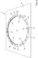
In
Die Basisplatte 10 weist in der Mitte ein Aufnahmeloch 12 für einen Wafer auf, der in der Mitte des Aufnahmelochs 12 angeordnet wird. Um das kreisförmige Aufnahmeloch 12 sind angrenzend in der Basisplatte 10 Taschen 14 ausgebildet, in denen Waferkontaktfinger 16, 18 alternierend in Umfangsrichtung des Aufnahmelochs 12 angeordnet sind. Die Waferkontaktfinger 16, 18 weisen entsprechende Schwenkachsen 26 bzw. 28 auf, um die die Waferkontaktfinger 16, 18 schwenkbar gelagert sind. Die Schwenkachsen 26, 28 sind hierbei senkrecht zur ebenen Oberfläche der Basisplatte 10 ausgerichtet.The
Oberhalb der Aufnahmetaschen 14 bzw. der darin angeordneten Waferkontaktfinger 16, 18 ist ein Stellring 20 angeordnet (vgl.
Der Stellring 20 weist Steuerkurven 22, 24 auf, in die die Vorsprünge 19 der Waferkontaktfinger 16, 18 eingreifen, wodurch der Stellring 20 mit den Waferkontaktfinger 16, 18 wirkverbunden ist. Bei einer relativen Verdrehung des Stellrings 20 gegenüber der Basisplatte 10 werden dadurch die Waferkontaktfinger 16, 18 aufgrund der Steuerkurven 22, 24 verschwenkt. Bei der in
Bei dem in den
Der Wafer-Chuck 1 ist beispielsweise Bestandteil eines Probenhalters und kann für eine Untersuchung mittels eines akustischen Rastermikroskops parallel zur Scanebene des Rastermikroskops justiert werden. Hierzu weist beispielsweise der Probenhalter entsprechende Justiermittel auf.The
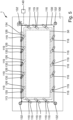
Entlang jeder Seite des rechteckförmigen Aufnahmelochs 112 sind auf dem Basiskörper 100 schwenkbare Waferkontaktfinger 116, 117, 118 für den Wafer 50 angeordnet. Die Waferkontaktfinger 116 sind hierbei als geradlinige, längserstreckte Körper ausgebildet. Der Waferkontaktfinger 117 ist als gebogener oder bogenförmiger Körper ausgebildet. Der gegenüber dem Waferkontaktfinger 117 angeordnete Waferkontaktfinger 118 ist als Auflagefinger ausgebildet, wobei der Waferkontaktfinger 118 eine entsprechende Auflagefläche 128 für den Wafer 50 aufweist.Pivotable
Die Waferkontaktfinger 116, 117, 118 sind verschwenkbar gelagert und weisen jeweils eine Schwenkachse 119 auf. Um die Waferkontaktfinger 116, 117, 118 um ihre Schwenkachsen 119 synchron zu verschwenken, sind die Waferkontaktfinger 116, 117, 118 mit einem geschlossenen Zugseil 130 verbunden.The
Das Zugseil 130 wird hierbei entlang der Seiten des rechteckförmigen Aufnahmelochs 112 geführt, wobei in den Ecken des rechteckförmigen Aufnahmelochs 112 Umlenkrollen 132 angeordnet sind, wobei das Zugseil 130 hierbei mit einem Umstellungswinkel von ungefähr 270° um die Umlenkrollen 132 geführt wird. Für eine der Umlenkrollen 132 ist ein Antrieb 140 vorgesehen, während die anderen Umlenkrollen 132 als mitlaufende Rollen ausgebildet sind. Das Zugseil 130 ist hierbei jeweils mit den Waferkontaktfingern 116, 117, 118 verbunden, so dass bei einer Bewegung des Zugseils 130 mittels der durch den Antrieb 140 angetriebenen Umlenkrolle 132 die Waferkontaktfinger 116, 117, 118 gleichzeitig verschwenkt werden.The
Der Waferkontaktfinger 118 mit der Auflagenfläche 128 ist gegensinnig zu den anderen Waferkontaktfingern 116, 117 gelagert, so dass die Schwenkbewegung bzw. Schwenkrichtung des Waferkontaktfingers 118 entgegen der Schwenkrichtung der anderen Waferkontaktfinger 116, 117 ist.The
Bei Anordnung des Wafers 50 in dem Aufnahmeloch 112 sind die Waferkontaktfinger 116, 117 weggeschwenkt, während der Waferkontaktfinger 118 mit der Auflagenfläche 128 eingeschwenkt ist, so dass der Wafer 50 in Kontakt mit der Auflagenfläche 128 des Waferkontaktfingers 118 gebracht ist bzw. darauf aufliegt. Im Rahmen der Erfindung können auch mehrere Waferkontaktfinger 118 mit jeweiligen Auflagenflächen 128 für den Wafer 50 am Aufnahmeloch 112 angeordnet sein. Danach werden die Waferkontaktfinger 116, 117 in Richtung des Wafers 50 geschwenkt, während der Waferkontaktfinger 118 vom Wafer 50 weggeschwenkt wird.When the
Um eine schwenksynchrone Schwenkbewegung der Waferkontaktfinger 116 auszuführen, sind die Waferkontaktfinger 116 mit dem Zugseil 130 verbunden, das um die Umlenkrolle 132 herumgeführt wird. Ferner ist das Zugseil 130 mit einer, insbesondere starren, Führungsstange 134 für die Waferkontaktfinger 126, die an einer (Längs-) Seite der Auflagefläche 113 angeordnet sind, verbunden, wobei die Führungsstange 134 entsprechende Steuerkurven 135 für die damit verbundenen Waferkontaktfinger 126 aufweist. Die Führungsstange 134 ist hierbei starr ausgebildet und mit dem Zugseil 130 verbunden, so dass bei Bewegung des Zugseils 130 die Führungsstange 134 linear bewegt wird, wodurch mittels der Steuerkurven 135 in der Führungsstange 134 die Waferkontaktfinger 126 eine synchrone Schwenkbewegung zusammen mit den Waferkontaktfinger 116, die mit dem Zugseil 130 direkt verbunden sind, ausführen.In order to carry out a pivoting-synchronous pivoting movement of the
BezugszeichenlisteList of reference symbols
- 11
- Wafer-ChuckWafer chuck
- 1010
- BasisplatteBase plate
- 1212
- AufnahmelochMounting hole
- 1414
- TascheBag
- 1616
- WaferkontaktfingerWafer contact fingers
- 1818
- WaferkontaktfingerWafer contact fingers
- 1919
- Vorsprunghead Start
- 2020
- StellringAdjusting ring
- 2222
- SteuerkurveControl curve
- 2424
- SteuerkurveControl curve
- 2626
- SchwenkachseSwivel axis
- 2929
- SchwenkachseSwivel axis
- 5050
- WaferWafer
- 100100
- BasiskörperBase body
- 112112
- AufnahmelochMounting hole
- 113113
- AuflageflächeSupport surface
- 116, 117, 118116, 117, 118
- WaferkontaktfingerWafer contact fingers
- 119119
- SchwenkachseSwivel axis
- 126126
- WaferkontaktfingerWafer contact fingers
- 128128
- AuflageflächeSupport surface
- 130130
- ZugseilPull rope
- 132132
- UmlenkrollenPulleys
- 134134
- FührungsstangeGuide rod
- 135135
- SteuerkurveControl curve
- 140140
- Antriebdrive
Claims (23)
Priority Applications (6)
| Application Number | Priority Date | Filing Date | Title |
|---|---|---|---|
| DE102021109210.8A DE102021109210B4 (en) | 2021-04-13 | 2021-04-13 | Wafer chuck for handling and transmitting a wafer in an acoustic scanning microscope, use of a wafer chuck and wafer processing device with a wafer chuck |
| TW111111969A TWI853227B (en) | 2021-04-13 | 2022-03-29 | Wafer chuck for handling a wafer |
| CN202210377721.9A CN115206866B (en) | 2021-04-13 | 2022-04-12 | Wafer chuck for handling wafers |
| US17/719,164 US20220328341A1 (en) | 2021-04-13 | 2022-04-12 | Wafer chuck for handling a wafer |
| KR1020220045624A KR102944815B1 (en) | 2021-04-13 | 2022-04-13 | Wafer chuck for handling one wafer |
| JP2022066228A JP7502363B2 (en) | 2021-04-13 | 2022-04-13 | Wafer chuck for handling wafers |
Applications Claiming Priority (1)
| Application Number | Priority Date | Filing Date | Title |
|---|---|---|---|
| DE102021109210.8A DE102021109210B4 (en) | 2021-04-13 | 2021-04-13 | Wafer chuck for handling and transmitting a wafer in an acoustic scanning microscope, use of a wafer chuck and wafer processing device with a wafer chuck |
Publications (2)
| Publication Number | Publication Date |
|---|---|
| DE102021109210A1 DE102021109210A1 (en) | 2022-10-13 |
| DE102021109210B4 true DE102021109210B4 (en) | 2024-07-25 |
Family
ID=83361712
Family Applications (1)
| Application Number | Title | Priority Date | Filing Date |
|---|---|---|---|
| DE102021109210.8A Active DE102021109210B4 (en) | 2021-04-13 | 2021-04-13 | Wafer chuck for handling and transmitting a wafer in an acoustic scanning microscope, use of a wafer chuck and wafer processing device with a wafer chuck |
Country Status (6)
| Country | Link |
|---|---|
| US (1) | US20220328341A1 (en) |
| JP (1) | JP7502363B2 (en) |
| KR (1) | KR102944815B1 (en) |
| CN (1) | CN115206866B (en) |
| DE (1) | DE102021109210B4 (en) |
| TW (1) | TWI853227B (en) |
Citations (6)
| Publication number | Priority date | Publication date | Assignee | Title |
|---|---|---|---|---|
| US5192087A (en) | 1990-10-02 | 1993-03-09 | Nippon Steel Corporation | Device for supporting a wafer |
| US6143147A (en) | 1998-10-30 | 2000-11-07 | Tokyo Electron Limited | Wafer holding assembly and wafer processing apparatus having said assembly |
| US20050193943A1 (en) | 2002-07-26 | 2005-09-08 | Dainippon Screen Mfg. Co., Ltd. | Substrate treatment method and substrate treatment apparatus |
| US20140077431A1 (en) | 2012-09-20 | 2014-03-20 | Varian Semiconductor Equipment Associates, Inc. | System and Method for 2D Workpiece Alignment |
| US20190148212A1 (en) | 2017-11-14 | 2019-05-16 | Taiwan Semiconductor Manufacturing Co., Ltd. | Semiconductor wafer cleaning apparatus and method for cleaning semiconductor wafer |
| US20200020563A1 (en) | 2017-03-27 | 2020-01-16 | SCREEN Holdings Co., Ltd. | Substrate processing device, substrate processing method, and program recording medium |
Family Cites Families (29)
| Publication number | Priority date | Publication date | Assignee | Title |
|---|---|---|---|---|
| JPS5790956A (en) * | 1980-11-28 | 1982-06-05 | Hitachi Ltd | Gripper for wafer |
| DE69021952T2 (en) * | 1989-06-29 | 1996-05-15 | Applied Materials Inc | Device for handling semiconductor wafers. |
| JPH04142054A (en) * | 1990-10-02 | 1992-05-15 | Nippon Steel Corp | Gripping device for wafer |
| US5566466A (en) * | 1994-07-01 | 1996-10-22 | Ontrak Systems, Inc. | Spindle assembly with improved wafer holder |
| EP0739671A3 (en) * | 1995-04-25 | 1997-07-23 | Daetwyler Ag | Tree support |
| US6217034B1 (en) * | 1998-09-24 | 2001-04-17 | Kla-Tencor Corporation | Edge handling wafer chuck |
| US6258228B1 (en) * | 1999-01-08 | 2001-07-10 | Tokyo Electron Limited | Wafer holder and clamping ring therefor for use in a deposition chamber |
| JP3909981B2 (en) | 1999-04-23 | 2007-04-25 | 株式会社 Sen−Shi・アクセリス カンパニー | Wafer size conversion holder and wafer holding method using the same |
| TW452917B (en) * | 1999-10-29 | 2001-09-01 | Winbond Electronics Corp | Holder |
| US6435807B1 (en) * | 2000-12-14 | 2002-08-20 | Genmark Automation | Integrated edge gripper |
| JP4488646B2 (en) * | 2001-04-23 | 2010-06-23 | 株式会社トプコン | Wafer holding device |
| US6752442B2 (en) * | 2001-11-09 | 2004-06-22 | Speedfam-Ipec Corporation | Workpiece handling end-effector and a method for processing workpieces using a workpiece handling end-effector |
| JP2003282681A (en) | 2002-03-26 | 2003-10-03 | Dainippon Screen Mfg Co Ltd | Substrate holding device and substrate processing device |
| US6932558B2 (en) * | 2002-07-03 | 2005-08-23 | Kung Chris Wu | Wafer aligner |
| US20040206304A1 (en) * | 2003-04-15 | 2004-10-21 | Menear John Edgar | Pressurized chuck for controlling backside wafer contamination |
| JP4467379B2 (en) | 2004-08-05 | 2010-05-26 | 大日本スクリーン製造株式会社 | Substrate processing equipment |
| US7538474B2 (en) * | 2005-03-30 | 2009-05-26 | National University Of Singapore | System and method for Micro Electro Mechanical System (MEMS) device characterization |
| US7408624B2 (en) | 2005-06-30 | 2008-08-05 | Asml Netherlands B.V. | Lithographic apparatus and device manufacturing method |
| JP2008198836A (en) * | 2007-02-14 | 2008-08-28 | Dainippon Screen Mfg Co Ltd | Substrate processing apparatus and substrate processing method |
| US7750657B2 (en) * | 2007-03-15 | 2010-07-06 | Applied Materials Inc. | Polishing head testing with movable pedestal |
| CN102935942B (en) * | 2011-08-16 | 2015-03-04 | 中芯国际集成电路制造(北京)有限公司 | Electronic control manipulator |
| US9418883B2 (en) * | 2013-07-03 | 2016-08-16 | Lam Research Ag | Device for holding wafer shaped articles |
| EP3097985B1 (en) * | 2015-05-29 | 2018-11-21 | Gerald Sebert GmbH | Positioning device |
| US9553010B2 (en) * | 2015-06-25 | 2017-01-24 | Coreflow Ltd. | Wafer gripper with non-contact support platform |
| JP7282494B2 (en) * | 2018-09-18 | 2023-05-29 | 株式会社Screenホールディングス | SUBSTRATE PROCESSING APPARATUS AND SUBSTRATE PROCESSING METHOD |
| US20210356439A1 (en) * | 2018-10-05 | 2021-11-18 | Sonix, Inc. | System, Method and Apparatus for Ultrasonic Inspection |
| CN112053965B (en) * | 2019-06-06 | 2024-05-17 | 北京北方华创微电子装备有限公司 | Wafer clamping device torque measurement system |
| JP7453757B2 (en) | 2019-07-26 | 2024-03-21 | 株式会社Screenホールディングス | Substrate processing equipment, substrate processing system, and substrate processing method |
| TWM598297U (en) * | 2020-03-30 | 2020-07-11 | 群翊工業股份有限公司 | Holding device for placing substrate |
-
2021
- 2021-04-13 DE DE102021109210.8A patent/DE102021109210B4/en active Active
-
2022
- 2022-03-29 TW TW111111969A patent/TWI853227B/en active
- 2022-04-12 CN CN202210377721.9A patent/CN115206866B/en active Active
- 2022-04-12 US US17/719,164 patent/US20220328341A1/en active Pending
- 2022-04-13 JP JP2022066228A patent/JP7502363B2/en active Active
- 2022-04-13 KR KR1020220045624A patent/KR102944815B1/en active Active
Patent Citations (6)
| Publication number | Priority date | Publication date | Assignee | Title |
|---|---|---|---|---|
| US5192087A (en) | 1990-10-02 | 1993-03-09 | Nippon Steel Corporation | Device for supporting a wafer |
| US6143147A (en) | 1998-10-30 | 2000-11-07 | Tokyo Electron Limited | Wafer holding assembly and wafer processing apparatus having said assembly |
| US20050193943A1 (en) | 2002-07-26 | 2005-09-08 | Dainippon Screen Mfg. Co., Ltd. | Substrate treatment method and substrate treatment apparatus |
| US20140077431A1 (en) | 2012-09-20 | 2014-03-20 | Varian Semiconductor Equipment Associates, Inc. | System and Method for 2D Workpiece Alignment |
| US20200020563A1 (en) | 2017-03-27 | 2020-01-16 | SCREEN Holdings Co., Ltd. | Substrate processing device, substrate processing method, and program recording medium |
| US20190148212A1 (en) | 2017-11-14 | 2019-05-16 | Taiwan Semiconductor Manufacturing Co., Ltd. | Semiconductor wafer cleaning apparatus and method for cleaning semiconductor wafer |
Also Published As
| Publication number | Publication date |
|---|---|
| DE102021109210A1 (en) | 2022-10-13 |
| TWI853227B (en) | 2024-08-21 |
| CN115206866B (en) | 2026-03-20 |
| JP2022163002A (en) | 2022-10-25 |
| CN115206866A (en) | 2022-10-18 |
| JP7502363B2 (en) | 2024-06-18 |
| KR102944815B1 (en) | 2026-03-27 |
| KR20220141758A (en) | 2022-10-20 |
| TW202240769A (en) | 2022-10-16 |
| US20220328341A1 (en) | 2022-10-13 |
Similar Documents
| Publication | Publication Date | Title |
|---|---|---|
| DE102010032894B4 (en) | Tem lamella, process for its preparation and apparatus for carrying out the process | |
| DE102013219901B4 (en) | Clamping table | |
| EP2001038B9 (en) | Charged particle beam device and method applied in a charged particle beam device | |
| DE4128571A1 (en) | EYEWEAR SCANNER | |
| EP2849649A2 (en) | X-ray detector and x-ray system | |
| DE102020201863A1 (en) | Clamping table and examination device | |
| EP0546305A1 (en) | Corpuscular optical analysing and/or processing of material specimen | |
| DE10039928B4 (en) | Device for automated testing, calibration and characterization of test adapters | |
| DE10309887A1 (en) | Cone-beam computed tomography system | |
| DE102008002832A1 (en) | Method and device for nondestructive detection of defects in the interior of semiconductor material | |
| EP2454583B1 (en) | Inspection system | |
| EP3601999A1 (en) | Device for carrying out bending tests on panel-shaped or beam-shaped samples | |
| WO2011127962A1 (en) | Method and device for contacting a row of contact surfaces with probe tips | |
| DE102012215909B4 (en) | Tool for chemical-mechanical planarization with multiple spindles | |
| DE102021109210B4 (en) | Wafer chuck for handling and transmitting a wafer in an acoustic scanning microscope, use of a wafer chuck and wafer processing device with a wafer chuck | |
| DE102023212215A1 (en) | Clamping table | |
| EP3194927B1 (en) | Breaking chamber for measuring a hardness of a test subject | |
| DE102012017662A1 (en) | Sample holder for grinding device of sample preparation device, comprises replaceable sacrificial stop elements vertically adjustable in normal direction, where grinding plane lying parallel to plane is formed by sacrificial stop elements | |
| DE102015213764B4 (en) | Sample holder, charged particle beam apparatus and observation method | |
| EP3430462B1 (en) | Device for inserting into an imaging system | |
| DE10151441B4 (en) | Arrangement and method for receiving and processing a thin wafer | |
| DE102018108974B3 (en) | Method for producing a TEM sample | |
| DE69221014T2 (en) | Apparatus for quality control of a semiconductor device | |
| DE102006005448B4 (en) | Acoustic scanning microscope and autofocus method | |
| DE3842757A1 (en) | PORTABLE GRID ELECTRON MICROSCOPE |
Legal Events
| Date | Code | Title | Description |
|---|---|---|---|
| R012 | Request for examination validly filed | ||
| R079 | Amendment of ipc main class |
Free format text: PREVIOUS MAIN CLASS: H01L0021683000 Ipc: H01L0021687000 |
|
| R016 | Response to examination communication | ||
| R016 | Response to examination communication | ||
| R018 | Grant decision by examination section/examining division | ||
| R020 | Patent grant now final | ||
| R079 | Amendment of ipc main class |
Free format text: PREVIOUS MAIN CLASS: H01L0021687000 Ipc: H10P0072760000 |