DE102013210942B4 - Light extraction substrate for an organic light emitting device and method of manufacturing the substrate - Google Patents
Light extraction substrate for an organic light emitting device and method of manufacturing the substrate Download PDFInfo
- Publication number
- DE102013210942B4 DE102013210942B4 DE102013210942.3A DE102013210942A DE102013210942B4 DE 102013210942 B4 DE102013210942 B4 DE 102013210942B4 DE 102013210942 A DE102013210942 A DE 102013210942A DE 102013210942 B4 DE102013210942 B4 DE 102013210942B4
- Authority
- DE
- Germany
- Prior art keywords
- light extraction
- texture
- substrate
- base layer
- layer
- Prior art date
- Legal status (The legal status is an assumption and is not a legal conclusion. Google has not performed a legal analysis and makes no representation as to the accuracy of the status listed.)
- Active
Links
Images


Classifications
-
- B—PERFORMING OPERATIONS; TRANSPORTING
- B32—LAYERED PRODUCTS
- B32B—LAYERED PRODUCTS, i.e. PRODUCTS BUILT-UP OF STRATA OF FLAT OR NON-FLAT, e.g. CELLULAR OR HONEYCOMB, FORM
- B32B7/00—Layered products characterised by the relation between layers; Layered products characterised by the relative orientation of features between layers, or by the relative values of a measurable parameter between layers, i.e. products comprising layers having different physical, chemical or physicochemical properties; Layered products characterised by the interconnection of layers
- B32B7/03—Layered products characterised by the relation between layers; Layered products characterised by the relative orientation of features between layers, or by the relative values of a measurable parameter between layers, i.e. products comprising layers having different physical, chemical or physicochemical properties; Layered products characterised by the interconnection of layers with respect to the orientation of features
-
- H—ELECTRICITY
- H10—SEMICONDUCTOR DEVICES; ELECTRIC SOLID-STATE DEVICES NOT OTHERWISE PROVIDED FOR
- H10K—ORGANIC ELECTRIC SOLID-STATE DEVICES
- H10K59/00—Integrated devices, or assemblies of multiple devices, comprising at least one organic light-emitting element covered by group H10K50/00
- H10K59/80—Constructional details
- H10K59/875—Arrangements for extracting light from the devices
- H10K59/877—Arrangements for extracting light from the devices comprising scattering means
-
- B—PERFORMING OPERATIONS; TRANSPORTING
- B32—LAYERED PRODUCTS
- B32B—LAYERED PRODUCTS, i.e. PRODUCTS BUILT-UP OF STRATA OF FLAT OR NON-FLAT, e.g. CELLULAR OR HONEYCOMB, FORM
- B32B3/00—Layered products comprising a layer with external or internal discontinuities or unevennesses, or a layer of non-planar shape; Layered products comprising a layer having particular features of form
- B32B3/26—Layered products comprising a layer with external or internal discontinuities or unevennesses, or a layer of non-planar shape; Layered products comprising a layer having particular features of form characterised by a particular shape of the outline of the cross-section of a continuous layer; characterised by a layer with cavities or internal voids ; characterised by an apertured layer
- B32B3/30—Layered products comprising a layer with external or internal discontinuities or unevennesses, or a layer of non-planar shape; Layered products comprising a layer having particular features of form characterised by a particular shape of the outline of the cross-section of a continuous layer; characterised by a layer with cavities or internal voids ; characterised by an apertured layer characterised by a layer formed with recesses or projections, e.g. hollows, grooves, protuberances, ribs
-
- B—PERFORMING OPERATIONS; TRANSPORTING
- B32—LAYERED PRODUCTS
- B32B—LAYERED PRODUCTS, i.e. PRODUCTS BUILT-UP OF STRATA OF FLAT OR NON-FLAT, e.g. CELLULAR OR HONEYCOMB, FORM
- B32B5/00—Layered products characterised by the non- homogeneity or physical structure, i.e. comprising a fibrous, filamentary, particulate or foam layer; Layered products characterised by having a layer differing constitutionally or physically in different parts
- B32B5/14—Layered products characterised by the non- homogeneity or physical structure, i.e. comprising a fibrous, filamentary, particulate or foam layer; Layered products characterised by having a layer differing constitutionally or physically in different parts characterised by a layer differing constitutionally or physically in different parts, e.g. denser near its faces
- B32B5/145—Variation across the thickness of the layer
-
- B—PERFORMING OPERATIONS; TRANSPORTING
- B32—LAYERED PRODUCTS
- B32B—LAYERED PRODUCTS, i.e. PRODUCTS BUILT-UP OF STRATA OF FLAT OR NON-FLAT, e.g. CELLULAR OR HONEYCOMB, FORM
- B32B7/00—Layered products characterised by the relation between layers; Layered products characterised by the relative orientation of features between layers, or by the relative values of a measurable parameter between layers, i.e. products comprising layers having different physical, chemical or physicochemical properties; Layered products characterised by the interconnection of layers
- B32B7/02—Physical, chemical or physicochemical properties
- B32B7/023—Optical properties
-
- H—ELECTRICITY
- H10—SEMICONDUCTOR DEVICES; ELECTRIC SOLID-STATE DEVICES NOT OTHERWISE PROVIDED FOR
- H10K—ORGANIC ELECTRIC SOLID-STATE DEVICES
- H10K50/00—Organic light-emitting devices
- H10K50/80—Constructional details
- H10K50/85—Arrangements for extracting light from the devices
- H10K50/854—Arrangements for extracting light from the devices comprising scattering means
-
- H—ELECTRICITY
- H10—SEMICONDUCTOR DEVICES; ELECTRIC SOLID-STATE DEVICES NOT OTHERWISE PROVIDED FOR
- H10K—ORGANIC ELECTRIC SOLID-STATE DEVICES
- H10K50/00—Organic light-emitting devices
- H10K50/80—Constructional details
- H10K50/85—Arrangements for extracting light from the devices
- H10K50/858—Arrangements for extracting light from the devices comprising refractive means, e.g. lenses
-
- H—ELECTRICITY
- H10—SEMICONDUCTOR DEVICES; ELECTRIC SOLID-STATE DEVICES NOT OTHERWISE PROVIDED FOR
- H10K—ORGANIC ELECTRIC SOLID-STATE DEVICES
- H10K59/00—Integrated devices, or assemblies of multiple devices, comprising at least one organic light-emitting element covered by group H10K50/00
- H10K59/80—Constructional details
- H10K59/875—Arrangements for extracting light from the devices
- H10K59/879—Arrangements for extracting light from the devices comprising refractive means, e.g. lenses
-
- H—ELECTRICITY
- H10—SEMICONDUCTOR DEVICES; ELECTRIC SOLID-STATE DEVICES NOT OTHERWISE PROVIDED FOR
- H10K—ORGANIC ELECTRIC SOLID-STATE DEVICES
- H10K71/00—Manufacture or treatment specially adapted for the organic devices covered by this subclass
-
- Y—GENERAL TAGGING OF NEW TECHNOLOGICAL DEVELOPMENTS; GENERAL TAGGING OF CROSS-SECTIONAL TECHNOLOGIES SPANNING OVER SEVERAL SECTIONS OF THE IPC; TECHNICAL SUBJECTS COVERED BY FORMER USPC CROSS-REFERENCE ART COLLECTIONS [XRACs] AND DIGESTS
- Y10—TECHNICAL SUBJECTS COVERED BY FORMER USPC
- Y10T—TECHNICAL SUBJECTS COVERED BY FORMER US CLASSIFICATION
- Y10T428/00—Stock material or miscellaneous articles
- Y10T428/24—Structurally defined web or sheet [e.g., overall dimension, etc.]
- Y10T428/24273—Structurally defined web or sheet [e.g., overall dimension, etc.] including aperture
-
- Y—GENERAL TAGGING OF NEW TECHNOLOGICAL DEVELOPMENTS; GENERAL TAGGING OF CROSS-SECTIONAL TECHNOLOGIES SPANNING OVER SEVERAL SECTIONS OF THE IPC; TECHNICAL SUBJECTS COVERED BY FORMER USPC CROSS-REFERENCE ART COLLECTIONS [XRACs] AND DIGESTS
- Y10—TECHNICAL SUBJECTS COVERED BY FORMER USPC
- Y10T—TECHNICAL SUBJECTS COVERED BY FORMER US CLASSIFICATION
- Y10T428/00—Stock material or miscellaneous articles
- Y10T428/24—Structurally defined web or sheet [e.g., overall dimension, etc.]
- Y10T428/24355—Continuous and nonuniform or irregular surface on layer or component [e.g., roofing, etc.]
-
- Y—GENERAL TAGGING OF NEW TECHNOLOGICAL DEVELOPMENTS; GENERAL TAGGING OF CROSS-SECTIONAL TECHNOLOGIES SPANNING OVER SEVERAL SECTIONS OF THE IPC; TECHNICAL SUBJECTS COVERED BY FORMER USPC CROSS-REFERENCE ART COLLECTIONS [XRACs] AND DIGESTS
- Y10—TECHNICAL SUBJECTS COVERED BY FORMER USPC
- Y10T—TECHNICAL SUBJECTS COVERED BY FORMER US CLASSIFICATION
- Y10T428/00—Stock material or miscellaneous articles
- Y10T428/24—Structurally defined web or sheet [e.g., overall dimension, etc.]
- Y10T428/24479—Structurally defined web or sheet [e.g., overall dimension, etc.] including variation in thickness
- Y10T428/24521—Structurally defined web or sheet [e.g., overall dimension, etc.] including variation in thickness with component conforming to contour of nonplanar surface
- Y10T428/24545—Containing metal or metal compound
-
- Y—GENERAL TAGGING OF NEW TECHNOLOGICAL DEVELOPMENTS; GENERAL TAGGING OF CROSS-SECTIONAL TECHNOLOGIES SPANNING OVER SEVERAL SECTIONS OF THE IPC; TECHNICAL SUBJECTS COVERED BY FORMER USPC CROSS-REFERENCE ART COLLECTIONS [XRACs] AND DIGESTS
- Y10—TECHNICAL SUBJECTS COVERED BY FORMER USPC
- Y10T—TECHNICAL SUBJECTS COVERED BY FORMER US CLASSIFICATION
- Y10T428/00—Stock material or miscellaneous articles
- Y10T428/24—Structurally defined web or sheet [e.g., overall dimension, etc.]
- Y10T428/24479—Structurally defined web or sheet [e.g., overall dimension, etc.] including variation in thickness
- Y10T428/24595—Structurally defined web or sheet [e.g., overall dimension, etc.] including variation in thickness and varying density
-
- Y—GENERAL TAGGING OF NEW TECHNOLOGICAL DEVELOPMENTS; GENERAL TAGGING OF CROSS-SECTIONAL TECHNOLOGIES SPANNING OVER SEVERAL SECTIONS OF THE IPC; TECHNICAL SUBJECTS COVERED BY FORMER USPC CROSS-REFERENCE ART COLLECTIONS [XRACs] AND DIGESTS
- Y10—TECHNICAL SUBJECTS COVERED BY FORMER USPC
- Y10T—TECHNICAL SUBJECTS COVERED BY FORMER US CLASSIFICATION
- Y10T428/00—Stock material or miscellaneous articles
- Y10T428/24—Structurally defined web or sheet [e.g., overall dimension, etc.]
- Y10T428/24479—Structurally defined web or sheet [e.g., overall dimension, etc.] including variation in thickness
- Y10T428/24612—Composite web or sheet
- Y10T428/2462—Composite web or sheet with partial filling of valleys on outer surface
Landscapes
- Physics & Mathematics (AREA)
- Optics & Photonics (AREA)
- Engineering & Computer Science (AREA)
- Manufacturing & Machinery (AREA)
- Electroluminescent Light Sources (AREA)
Abstract
Substrat zur Lichtextraktion für eine organische lichtemittierende Vorrichtung, aufweisend einen Oxid- oder Nitriddünnfilm (100), der auf einem Substratkörper (11) ausgebildet ist, wobei der Oxid- oder Nitriddünnfilm (100) aufweist:
eine Basisschicht (110), die auf dem Substratkörper (11) ausgebildet ist;
eine erste Textur (120), die auf der Basisschicht (110) ausgebildet ist, wobei die erste Textur (120) eine Vielzahl erster Vorsprünge (121) aufweist, die aus der Basisschicht (120) vorragen; und
eine zweite Textur (130), die eine Vielzahl zweiter Vorsprünge (131) aufweist, die aus jeder Außenfläche der ersten Vorsprünge (121) vorragen, wobei
eine Dicke (a1) der Basisschicht (110) 25% oder weniger einer Dicke der ersten Textur (120) beträgt, wobei die Dicke der ersten Textur (120) mit einer Höhe (b1) des höchsten Vorsprungs der Vielzahl der ersten Vorsprünge (121) übereinstimmt,
und wobei die Kristallstruktur der Basisschicht (110) dichter als die Kristallstruktur der ersten Textur (120) ist, sodass die Basisschicht (110) weniger Leerstellen in der Basisschicht (110) aufweist als die erste Textur (120).

a base layer (110) formed on the substrate body (11);
a first texture (120) formed on the base layer (110), the first texture (120) having a plurality of first protrusions (121) protruding from the base layer (120); and
a second texture (130) having a plurality of second projections (131) projecting from each outer surface of the first projections (121), wherein
a thickness (a1) of the base layer (110) is 25% or less of a thickness of the first texture (120), the thickness of the first texture (120) having a height (b1) of the highest protrusion of the plurality of first protrusions (121) agrees,
and wherein the crystal structure of the base layer (110) is denser than the crystal structure of the first texture (120) such that the base layer (110) has fewer voids in the base layer (110) than the first texture (120).
Description
HINTERGRUND DER ERFINDUNGBACKGROUND OF THE INVENTION
Gebiet der Erfindungfield of invention
Die vorliegende Erfindung betrifft ein Substrat zur Lichtextraktion für eine organische lichtemittierende Vorrichtung (OLED) und ein Verfahren zur Herstellung des Substrats, insbesondere betrifft sie ein Substrat zur Lichtextraktion für eine OLED, das die Helligkeit einer Anzeige oder eines Beleuchtungssystems, für die/das eine OLED verwendet wird, durch die Erhöhung der Lichtextraktionseffizienz verbessert, und ein Verfahren zur Herstellung des Substrats.The present invention relates to a light extraction substrate for an organic light emitting device (OLED) and a method for manufacturing the substrate, in particular it relates to a light extraction substrate for an OLED, which improves the brightness of a display or a lighting system for the OLED is used is improved by increasing the light extraction efficiency, and a method of manufacturing the substrate.
Beschreibung des Standes der TechnikDescription of the prior art
Allgemein weist eine organische lichtemittierende Vorrichtung (OLED) eine Anode, eine lichtemittierende Schicht und eine Kathode auf. Liegt eine Spannung zwischen der Anode und der Kathode an, so werden Löcher von der Anode in die organische lichtemittierende Schicht injiziert und werden Elektronen von der Kathode in die organische lichtemittierende Schicht injiziert. Löcher und Elektronen, die in die organische lichtemittierende Schicht gewandert sind, rekombinieren miteinander in der organischen lichtemittierenden Schicht, so dass Exzitonen erzeugt werden. Wenn diese Exzitonen vom angeregten Zustand in den Grundzustand übergehen, wird Licht emittiert.In general, an organic light-emitting device (OLED) has an anode, a light-emitting layer, and a cathode. When a voltage is applied between the anode and the cathode, holes are injected into the organic light-emitting layer from the anode, and electrons are injected into the organic light-emitting layer from the cathode. Holes and electrons that have migrated into the organic light-emitting layer recombine with each other in the organic light-emitting layer to generate excitons. When these excitons transition from the excited state to the ground state, light is emitted.
Organische lichtemittierende Anzeigen, die eine OLED aufweisen, lassen sich je nach dem Mechanismus der Ansteuerung einer N*M Anzahl von Pixeln, die in Form einer Matrix angeordnet sind, in einen Passiv-Matrix-Typ und einen Aktiv-Matrix-Typ unterteilen.Organic light emitting displays comprising an OLED are classified into a passive matrix type and an active matrix type according to the mechanism of driving an N*M number of pixels arranged in the form of a matrix.
Beim Aktiv-Matrix-Typ sind eine Pixelelektrode, die einen lichtemittierenden Bereich definiert, und eine Schaltung zur Ansteuerung einer Pixeleinheit, die einen Strom oder eine Spannung an die Pixelelektrode anlegt, in einem Pixeleinheitsbereich positioniert. Die Schaltung zur Ansteuerung einer Pixeleinheit weist zumindest zwei Dünnfilmtransistoren (TFTs) und einen Kondensator auf. Dank dieser Konfiguration kann die Schaltung zur Ansteuerung einer Pixeleinheit unabhängig von der Anzahl der Pixel einen konstanten Strom zuführen und ermöglicht so eine gleichmäßige Leuchtdichte. Zudem verbraucht die organische lichtemittierende Anzeige des Aktiv-Matrix-Typs wenig Energie, so dass sie vorteilhaft für hochauflösende Anzeigen und große Anzeigen verwendet werden kann. Der Passiv-Matrix-Typ ist hingegen derart konfiguriert, dass Strom direkt an jedem Pixel anliegt. Obwohl der Passiv-Matrix-Typ einfacher als der Aktiv-Matrix-Typ aufgebaut ist, ist er für eine hochauflösende Anzeige ungeeignet. Daher wird der Passiv-Matrix-Typ im Allgemeinen für kleine Anzeigen oder Beleuchtungssysteme verwendet.In the active matrix type, a pixel electrode that defines a light-emitting area and a pixel unit driving circuit that applies a current or a voltage to the pixel electrode are positioned in a pixel unit area. The circuit for driving a pixel unit has at least two thin film transistors (TFTs) and a capacitor. This configuration enables the circuit to drive a unit pixel to supply a constant current regardless of the number of pixels, enabling uniform luminance. In addition, the active matrix type organic light emitting display consumes little power, so that it can be advantageously used for high definition displays and large displays. On the other hand, the passive matrix type is configured so that current is applied directly to each pixel. Although the passive matrix type is simpler in structure than the active matrix type, it is unsuitable for a high-resolution display. Therefore, the passive matrix type is generally used for small displays or lighting systems.
Obgleich OLEDs kommerziell vertrieben werden, kommt es aufgrund der Differenz zwischen Brechungsindices an der Schnittstelle zwischen der Dünnfilmschicht der Vorrichtung und des Substrats immer noch zu Lichtverlust. Infolgedessen ist die Lichtextraktionseffizienz von OLEDs auf etwa 20% begrenzt, was problematisch ist. Bei OLEDs besteht die Schwierigkeit darin, ohne Erhöhung der Lichtextraktionseffizienz eine hohe Effizienz zu erzielen.Although OLEDs are commercially available, light leakage still occurs at the interface between the thin film layer of the device and the substrate due to the difference in refractive indices. As a result, the light extraction efficiency of OLEDs is limited to around 20%, which is problematic. The difficulty with OLEDs is to achieve high efficiency without increasing light extraction efficiency.
Zur Lösung dieses Problems wurde ein Ansatz zur Erhöhung der optischen Effizienz durch Ausbildung einer Lichtextraktionsschicht auf einer OLED vorgeschlagen. Im Stand der Technik wurden solche Lichtextraktionsschichten mittels Fotolithographie ausgebildet. Durch den Einsatz aufwändiger Einrichtungen ist dies indes kostspielig und erfordert ein kompliziertes Verfahren, was problematisch ist.To solve this problem, an approach of increasing optical efficiency by forming a light extraction layer on an OLED has been proposed. In the prior art, such light extraction layers were formed using photolithography. However, due to the use of complex equipment, this is expensive and requires a complicated process, which is problematic.
Außerdem wurde die Lichtextraktionsschicht durch Mustern eines Polymerkunststofffilms und anschließendes Befestigen des gemusterten Films auf einer OLED ausgebildet. Dieses Verfahren unterliegt jedoch Beschränkungen hinsichtlich des Anstiegs des Brechungsindex' des Polymerkunststoffmaterials ebenso wie hinsichtlich der mechanischen Lebensdauer und der Temperaturbelastbarkeit des Materials. Substrate zur Lichtextraktion sind etwa in
Die im Hintergrund der Erfindung offenbarten Angaben dienen lediglich dem besseren Verständnis des Hintergrunds der Erfindung und sind nicht als eine Anerkennung oder irgendeine Form der Andeutung, dass diese Angaben einen dem Fachmann bereits bekannten Stand der Technik bilden, zu verstehen.The information disclosed in the background of the invention is only for enhancement of understanding of the background of the invention and should not be taken as an acknowledgment or any form of implication that this information forms the prior art already known to a person skilled in the art.
KURZZUSAMMENFASSUNG DER ERFINDUNGBRIEF SUMMARY OF THE INVENTION
Verschiedene Aspekte der vorliegenden Erfindung stellen ein Substrat zur Lichtextraktion für eine organische lichtemittierende Vorrichtung (OLED) bereit, das die Helligkeit einer Anzeige oder eines Beleuchtungssystems, für die/das eine OLED verwendet wird, durch die Erhöhung der Lichtextraktionseffizienz verbessern kann, und ein Verfahren zur Herstellung des Substrats.Various aspects of the present invention provide a light extraction substrate for an organic light emitting device (OLED) that can improve the brightness of a display or lighting system using an OLED by increasing light extraction efficiency, and a method for Preparation of the substrate.
Gemäß einem Aspekt der vorliegenden Erfindung wird ein Substrat zur Lichtextraktion für eine organische lichtemittierende Vorrichtung (OLED) gemäß Anspruch 1 bereitgestellt. Das Substrat zur Lichtextraktion weist einen Oxid- oder Nitriddünnfilm auf, der auf einem Substratkörper ausgebildet ist. Der Oxid- oder Nitriddünnfilm weist Folgendes auf: eine Basisschicht, die auf dem Substratkörper ausgebildet ist, eine erste Textur, die auf der Basisschicht ausgebildet ist, wobei die erste Textur eine Vielzahl erster Vorsprünge aufweist, die kontinuierlich oder diskontinuierlich aus der Basisschicht vorragen; und eine zweite Textur, die eine Vielzahl zweiter Vorsprünge aufweist, die kontinuierlich oder diskontinuierlich aus jeder Außenfläche der ersten Vorsprünge vorragen.According to one aspect of the present invention, a light extraction substrate for an organic light emitting device (OLED) according to
Gemäß einer Ausführungsform der vorliegenden Erfindung kann der Brechungsindex des Oxid- oder Nitriddünnfilms größer als der Brechungsindex des Substratkörpers sein.According to an embodiment of the present invention, the refractive index of the oxide or nitride thin film can be larger than the refractive index of the substrate body.
Die (vorzugsweise durchschnittliche) Dicke des Oxid- oder Nitriddünnfilms kann im Bereich von 1 bis 12 µm liegen.The (preferably average) thickness of the oxide or nitride thin film can range from 1 to 12 µm.
Die (vorzugsweise durchschnittliche) Dicke der Basisschicht beträgt 25% oder weniger der Dicke der ersten Textur.The (preferably average) thickness of the base layer is 25% or less of the thickness of the first texture.
Die Basisschicht weist weniger Leerstellen in der Basisschicht (d. h. Leerstellen, die vollständig in der Basisschicht eingeschlossen sind) auf als die erste Textur (d. h. Leerstellen, die vollständig in der ersten Textur eingeschlossen sind). Anders ausgedrückt, die Kristallstruktur der Basisschicht ist dichter als die Kristallstruktur der ersten Textur.The base layer has fewer base layer voids (i.e., voids completely enclosed in the base layer) than the first texture (i.e., voids completely enclosed in the first texture). In other words, the crystal structure of the base layer is denser than the crystal structure of the first texture.
Der Oxid- oder Nitriddünnfilm kann aus einem bestehen, das aus der Gruppe bestehend aus ZnO, TiO2, SnO2, SrTiO3, VO2, V2O3, SrRuO3, Si3N4, SiN, TiN, SiO2 und deren Mischungen ausgewählt ist.The oxide or nitride thin film may be one selected from the group consisting of ZnO, TiO 2 , SnO 2 , SrTiO 3 , VO 2 , V 2 O 3 , SrRuO 3 , Si 3 N 4 , SiN, TiN, SiO 2 and whose mixture is selected.
Der Oxid- oder Nitriddünnfilm kann einen Dotierstoff aus zumindest einem aufweisen, das aus einer Stoffgruppe bestehend aus Mg, Cd, S, Se, Te, F, Ga, Al, Mn, Co, Cu, Nb, Nd, Sr, W und Fe ausgewählt ist.The oxide or nitride thin film may have a dopant of at least one selected from a group consisting of Mg, Cd, S, Se, Te, F, Ga, Al, Mn, Co, Cu, Nb, Nd, Sr, W and Fe is selected.
Das Substrat zur Lichtextraktion kann eine durchschnittliche Lichtdurchlässigkeit von 40% oder mehr in einem Wellenlängenbereich von 380 bis 800 nm aufweisen.The light extraction substrate may have an average light transmittance of 40% or more in a wavelength range of 380 to 800 nm.
Die (vorzugsweise durchschnittliche) Dicke der Basisschicht kann im Bereich von 0,01 bis 1 µm liegen.The (preferably average) thickness of the base layer can range from 0.01 to 1 µm.
Die Höhe jedes der ersten Vorsprünge kann im Bereich von 0,05 bis 10 µm liegen.The height of each of the first protrusions may range from 0.05 to 10 µm.
Der Abstand jedes der ersten Vorsprünge kann 10 µm oder weniger betragen.The pitch of each of the first projections may be 10 µm or less.
Die kleinste Breite jedes der ersten Vorsprünge kann im Bereich von 0,05 bis 5 µm liegen, und die Erstreckung (Breite) des jeweiligen ersten Vorsprungs, die sich orthogonal zur jeweiligen kleinsten Breite erstreckt, kann im Bereich von 0,05 bis 10 µm liegen.The smallest width of each of the first protrusions may range from 0.05 to 5 µm, and the extent (width) of each first protrusion, which extends orthogonally to the respective smallest width, may range from 0.05 to 10 µm .
Der Abstand jedes der zweiten Vorsprünge kann im Bereich von 0,01 bis 1 µm liegen, und die Höhe jedes der zweiten Vorsprünge kann im Bereich von 0,01 bis 1 µm liegen.The pitch of each of the second protrusions may range from 0.01 to 1 µm and the height of each of the second protrusions may range from 0.01 to 1 µm.
Vorzugsweise sind die zweiten Vorsprünge auf den Oberflächen der ersten Vorsprünge positioniert. Besonders bevorzugt sind die zweiten Vorsprünge ausschließlich auf den Außenflächen der ersten Vorsprünge positioniert.Preferably, the second protrusions are positioned on the surfaces of the first protrusions. More preferably, the second protrusions are positioned exclusively on the outer surfaces of the first protrusions.
Das Substrat zur Lichtextraktion besteht vorzugsweise aus einem Oxid- oder Nitriddünnfilm, der auf einem Substratkörper ausgebildet ist. Das heißt, dass alle Komponenten des Substrats zur Lichtextraktion (Basisschicht, erste Textur und zweite Textur) aus einem Oxid oder aus einem Nitrid bestehen.The substrate for light extraction is preferably composed of an oxide or nitride thin film formed on a substrate body. That is, all components of the light extraction substrate (base layer, first texture, and second texture) are made of an oxide or a nitride.
Vorzugsweise sind die ersten Vorsprünge in einem regelmäßigen Muster ausgebildet. Vorzugsweise sind die ersten Vorsprünge gleichmäßig über einen lichtemittierenden Bereich des Substratkörpers verteilt. Vorzugsweise ist der lichtemittierende Bereich des Substratkörpers ein solcher Bereich des Substratkörpers, in dem eine Verlängerung der lichtemittierenden Schicht der OLED in die Ebene des Substratkörpers mit dem Substratkörper überlappt (Verlängerung entlang einer zur lichtemittierenden Schicht senkrechten Achse). Vorzugsweise liegt ein Verhältnis einer maximalen Höhe der ersten Vorsprünge und einer minimalen Höhe der ersten Vorsprünge (bezüglich aller Vorsprünge) im Bereich zwischen 10 und 1, besonders bevorzugt zwischen 5 und 1, noch mehr bevorzugt zwischen 3 und 1, noch mehr bevorzugt zwischen 2 und 1 und ganz besonders bevorzugt zwischen 1,5 und 1. Vorzugsweise liegt ein Verhältnis einer maximalen Breite der ersten Vorsprünge und einer minimalen Breite der ersten Vorsprünge (bezüglich aller Vorsprünge) im Bereich zwischen 10 und 1, besonders bevorzugt zwischen 5 und 1, noch mehr bevorzugt zwischen 3 und 1, noch mehr bevorzugt zwischen 2 und 1 und ganz besonders bevorzugt zwischen 1,5 und 1. Vorzugsweise liegt ein Verhältnis eines maximalen Abstands der ersten Vorsprünge und eines minimalen Abstands der ersten Vorsprünge (bezüglich aller Vorsprünge) im Bereich zwischen 10 und 1, besonders bevorzugt zwischen 5 und 1, noch mehr bevorzugt zwischen 3 und 1, noch mehr bevorzugt zwischen 2 und 1 und ganz besonders bevorzugt zwischen 1,5 und 1. Vorzugsweise sind jeweils die Höhe /Breite und der Abstand der Vielzahl der ersten Vorsprünge vollkommen gleichmäßig.Preferably, the first projections are formed in a regular pattern. The first projections are preferably distributed uniformly over a light-emitting area of the substrate body. The light-emitting region of the substrate body is preferably a region of the substrate body in which an extension of the light-emitting layer of the OLED in the plane of the substrate body overlaps with the substrate body (extension along an axis perpendicular to the light-emitting layer). Preferably, a ratio of a maximum height of the first protrusions and a minimum height of the first protrusions (with respect to all protrusions) is in the range between 10 and 1, more preferably between 5 and 1, even more preferably between 3 and 1, even more preferably between 2 and 2 1 and very particularly preferably between 1.5 and 1. Preferably, a ratio of a maximum width of the first projections and a minimum width of the first projections (with respect to all projections) is in the range between 10 and 1, particularly preferably between 5 and 1, even more preferably between 3 and 1, even more preferably between 2 and 1 and very particularly preferably between 1.5 and 1. Preferably, a ratio of a maximum distance of the first protrusions and a minimum distance of the first protrusions (with respect to all protrusions) is in the range between 10 and 1, more preferably between 5 and 1, even more preferably between 3 and 1, even more preferably between 2 and 1 µm d is most preferably between 1.5 and 1. Preferably, the height/width and the spacing of the plurality of first projections are completely uniform.
Vorzugsweise sind die zweiten Vorsprünge in einem regelmäßigen Muster ausgebildet. Vorzugsweise sind die zweiten Vorsprünge gleichmäßig über die Außenflächen der ersten Vorsprünge verteilt. Vorzugsweise sind die ersten Vorsprünge gleichmäßig über einen lichtemittierenden Bereich des Substratkörpers verteilt. Vorzugsweise liegt ein Verhältnis einer maximalen Höhe der zweiten Vorsprünge und einer minimalen Höhe der zweiten Vorsprünge (bezüglich aller Vorsprünge) im Bereich zwischen 10 und 1, besonders bevorzugt zwischen 5 und 1, noch mehr bevorzugt zwischen 3 und 1, noch mehr bevorzugt zwischen 2 und 1 und ganz besonders bevorzugt zwischen 1,5 und 1. Vorzugsweise liegt ein Verhältnis eines maximalen Abstands der zweiten Vorsprünge und eines minimalen Abstands der zweiten Vorsprünge (bezüglich aller Vorsprünge) im Bereich zwischen 10 und 1, besonders bevorzugt zwischen 5 und 1, noch mehr bevorzugt zwischen 3 und 1, noch mehr bevorzugt zwischen 2 und 1 und ganz besonders bevorzugt zwischen 1,5 und 1. Vorzugsweise sind jeweils die Höhe /Breite und der Abstand der Vielzahl der zweiten Vorsprünge vollkommen gleichmäßig.Preferably, the second projections are formed in a regular pattern. Preferably, the second projections are evenly distributed over the outer surfaces of the first projections. The first projections are preferably distributed uniformly over a light-emitting area of the substrate body. Preferably, a ratio of a maximum height of the second protrusions and a minimum height of the second protrusions (with respect to all protrusions) is in the range between 10 and 1, more preferably between 5 and 1, even more preferably between 3 and 1, even more preferably between 2 and 2 1 and very particularly preferably between 1.5 and 1. Preferably, a ratio of a maximum distance of the second projections and a minimum distance of the second projections (with respect to all projections) is in the range between 10 and 1, particularly preferably between 5 and 1, even more preferably between 3 and 1, even more preferably between 2 and 1 and very particularly preferably between 1.5 and 1. Preferably, the height/width and spacing of the plurality of second projections are completely uniform.
Vorzugsweise liegt ein Verhältnis der durchschnittlichen Höhe der ersten Vorsprünge und der durchschnittlichen Höhe der zweiten Vorsprünge (bezüglich aller Vorsprünge) im Bereich zwischen 100 und 1, besonders bevorzugt zwischen 50 und 2, noch mehr bevorzugt zwischen 30 und 4 und ganz besonders bevorzugt zwischen 20 und 5. Vorzugsweise liegt ein Verhältnis des durchschnittlichen Abstands der ersten Vorsprünge und des durchschnittlichen Abstands der zweiten Vorsprünge (bezüglich aller Vorsprünge) im Bereich zwischen 50 und 1, besonders bevorzugt zwischen 25 und 2, noch mehr bevorzugt zwischen 15 und 4 und ganz besonders bevorzugt zwischen 10 und 5.Preferably, a ratio of the average height of the first protrusions and the average height of the second protrusions (with respect to all protrusions) is in the range between 100 and 1, more preferably between 50 and 2, even more preferably between 30 and 4 and most preferably between 20 and 5. Preferably, a ratio of the average first protrusion pitch and the average second protrusion pitch (with respect to all the protrusions) ranges between 50 and 1, more preferably between 25 and 2, even more preferably between 15 and 4, and most preferably between 10 and 5
Gemäß einem weiteren Aspekt der vorliegenden Erfindung wird eine organische lichtemittierende Vorrichtung (OLED) bereitgestellt, die das durch die vorliegende Erfindung definierte Substrat zur Lichtextraktion aufweist, das als vorderes Substrat (oder hinteres Substrat) fungiert. Die OLED weist weiterhin ein hinteres Substrat (oder vorderes Substrat), das derart angeordnet ist, dass es dem weiteren Substrat zugewandt ist, eine erste und zweite Elektrodenschicht, die zwischen dem vorderen Substrat (Substratkörper) und dem hinteren Substrat angeordnet sind, eine organische lichtemittierende Schicht, die zwischen der ersten und zweiten Elektrodenschicht angeordnet ist, auf. Vorzugsweise weist die OLED weiterhin ein Dichtungsmittel auf, das auf dem Umfang des vorderen Substrats (Substratkörper) und des hinteren Substrats und in dem Raum zwischen dem vorderen Substrat (Substratkörper) und dem hinteren Substrat angeordnet ist, um die erste und zweite Elektrodenschicht und die organische lichtemittierende Schicht vor der Außenumgebung zu schützen. Gemäß der vorliegenden Erfindung weist die organische lichtemittierende Vorrichtung ein in der vorliegenden Erfindung definiertes Substrat zur Lichtextraktion auf. Das Substrat zur Lichtextraktion fungiert vorzugsweise als vorderes Substrat, das Substrat zur Lichtextraktion kann jedoch alternativ als hinteres Substrat fungieren.According to another aspect of the present invention, there is provided an organic light emitting device (OLED) having the light extraction substrate defined by the present invention functioning as a front (or back) substrate. The OLED further comprises a back substrate (or front substrate) arranged to face the further substrate, first and second electrode layers arranged between the front substrate (substrate body) and the back substrate, an organic light emitting Layer disposed between the first and second electrode layers. Preferably, the OLED further comprises a sealant disposed on the periphery of the front substrate (substrate body) and the back substrate and in the space between the front substrate (substrate body) and the back substrate to seal the first and second electrode layers and the organic to protect the light-emitting layer from the outside environment. According to the present invention, the organic light emitting device has a light extraction substrate defined in the present invention. The light extraction substrate preferably functions as the front substrate, but the light extraction substrate may alternatively function as the rear substrate.
Gemäß noch einem weiteren Aspekt der vorliegenden Erfindung wird ein Verfahren zur Herstellung eines Substrats zur Lichtextraktion gemäß Anspruch 12 bereitgestellt. Das Verfahren weist den Schritt der Ausbildung einer Lichtextraktionsschicht auf einem Substratkörper mittels einer chemischen Gasphasenabscheidung bei Atmosphärendruck (APCVD) auf, wobei die Lichtextraktionsschicht als Oxid- oder Nitriddünnfilm realisiert wird. Die Lichtextraktionsschicht weist eine Basisschicht auf dem Substratkörper, eine erste Textur, die eine Vielzahl erster Vorsprünge aufweist, die kontinuierlich oder diskontinuierlich aus der Basisschicht vorragen, und eine zweite Textur auf, die eine Vielzahl zweiter Vorsprünge aufweist, die kontinuierlich oder diskontinuierlich aus jeder Außenfläche der ersten Vorsprünge vorragen.According to a still further aspect of the present invention, a method of manufacturing a light extraction substrate according to
Gemäß einer Ausführungsform der vorliegenden Erfindung kann das Verfahren weiterhin den Schritt der Behandlung des Substrats mit Plasma oder einer Chemikalie vor dem Schritt der Ausbildung der Lichtextraktionsschicht mittels APCVD aufweisen.According to an embodiment of the present invention, the method may further comprise the step of treating the substrate with plasma or a chemical prior to the step of forming the light extraction layer by APCVD.
Gemäß einer Ausführungsform der vorliegenden Erfindung kann das Verfahren weiterhin den Schritt der Behandlung der Lichtextraktionsschicht mit Plasma oder einer Chemikalie nach dem Schritt der Ausbildung der Lichtextraktionsschicht mittels APCVD aufweisen.According to an embodiment of the present invention, the method may further comprise the step of treating the light extraction layer with plasma or a chemical after the step of forming the light extraction layer by APCVD.
Gemäß Ausführungsformen der vorliegenden Erfindung ist es möglich, die Lichtextraktionseffizienz durch die Bereitstellung eines Substrats zur Lichtextraktion zu verbessern, in dem Texturen, die verschiedene Größen und Formen aufweisen, auf mehreren Schichten ausgebildet sind. Infolgedessen lässt sich die Helligkeit einer Anzeige oder eines Beleuchtungssystems verbessern, für die/das eine OLED verwendet wird.According to embodiments of the present invention, it is possible to improve light extraction efficiency by providing a light extraction substrate in which textures having various sizes and shapes are formed on multiple layers. As a result, the brightness of a display or a lighting system using an OLED can be improved.
Zudem ist es möglich, natürlicherweise eine Textur auf der Oberfläche einer Lichtextraktionsschicht auszubilden, die mittels APCVD ausgebildet wird, was das Verfahren gegenüber dem Stand der Technik vereinfacht.In addition, it is possible to naturally form a texture on the surface of a light extraction layer formed by APCVD, which simplifies the process over the prior art.
Weiterhin kann eine OLED realisiert werden, die kostengünstig und hocheffizient ist.Furthermore, an OLED that is inexpensive and highly efficient can be realized.
Die Verfahren und Vorrichtungen gemäß der vorliegenden Erfindung weisen weitere Merkmale und Vorteile auf, die sich aus den hierin aufgenommenen beigefügten Figuren und der nachfolgenden ausführlichen Beschreibung der Erfindung ergeben oder in diesen genauer erläutert werden, wobei die Figuren und die Beschreibung gemeinsam der Erläuterung bestimmter Prinzipien der vorliegenden Erfindung dienen.The methods and apparatus of the present invention have additional features and advantages which will become apparent from or will be explained in more detail in the accompanying figures incorporated herein and the following detailed description of the invention, which figures and description together serve to explain certain principles of the invention serve the present invention.
Figurenlistecharacter list
-
1 zeigt eine Konfiguration, in der schematisch eine organische lichtemittierende Vorrichtung (OLED) dargestellt ist, die ein Substrat zur Lichtextraktion gemäß einer Ausführungsform der vorliegenden Erfindung aufweist;1 Fig. 12 shows a configuration schematically showing an organic light emitting device (OLED) having a substrate for light extraction according to an embodiment of the present invention; -
2 zeigt eine Ansicht, in der die Oberflächenform eines Substrats zur Lichtextraktion gemäß einer Ausführungsform der vorliegenden Erfindung dargestellt ist;2 12 is a view showing the surface shape of a substrate for light extraction according to an embodiment of the present invention; -
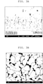
3A ,3B ,4A ,4B ,5A und5B zeigen Bilder eines Substrats zur Lichtextraktion gemäß einer Ausführungsform der vorliegenden Erfindung;3A ,3B ,4A ,4B ,5A and5B -
6 zeigt ein Diagramm, in dem die Korrelation zwischen der Gesamtdicke und der Lichtextraktionseffizienz einer Lichtextraktionsschicht gemäß einer Ausführungsform der vorliegenden Erfindung dargestellt ist;6 Fig. 12 is a graph showing the correlation between the total thickness and the light extraction efficiency of a light extraction layer according to an embodiment of the present invention; -
7 zeigt ein Diagramm, in dem die Korrelation zwischen der Dicke einer Basisschicht und der Lichtextraktionseffizienz einer Lichtextraktionsschicht gemäß einer Ausführungsform der vorliegenden Erfindung dargestellt ist;7 Fig. 12 is a graph showing the correlation between the thickness of a base layer and the light extraction efficiency of a light extraction layer according to an embodiment of the present invention; -
8 zeigt ein Diagramm, in dem die Korrelation zwischen der Dicke einer ersten Textur und der Lichtextraktionseffizienz einer Lichtextraktionsschicht gemäß einer Ausführungsform der vorliegenden Erfindung dargestellt ist;8th -
9 und10 zeigen Diagramme, in denen Veränderungen bei der Lichtdurchlässigkeit und dem Trübungswert in Abhängigkeit von der Wellenlänge eines Substrats zur Lichtextraktion gemäß einer Ausführungsform der vorliegenden Erfindung dargestellt sind; und9 and10 12 are graphs showing changes in transmittance and haze value with wavelength of a substrate for light extraction according to an embodiment of the present invention; and -
11 und12 zeigen Diagramme, in denen Veränderungen bei der Lichtdurchlässigkeit und dem Trübungswert in Abhängigkeit von der Wellenlänge eines Substrats zur Lichtextraktion gemäß dem Stand der Technik dargestellt sind.11 and12 12 are graphs showing changes in transmittance and haze value with respect to wavelength of a prior art substrate for light extraction.
AUSFÜHRLICHE BESCHREIBUNG DER ERFINDUNGDETAILED DESCRIPTION OF THE INVENTION
Nachfolgend soll ausführlich auf ein Substrat zur Lichtextraktion für eine organische lichtemittierende Vorrichtung (OLED) und ein Verfahren zur Herstellung des Substrats gemäß der vorliegenden Erfindung eingegangen werden, wobei Ausführungsformen der vorliegenden Erfindung in den beigefügten Figuren dargestellt und weiter unten beschrieben werden, so dass ein Durchschnittsfachmann in der Technik, auf die sich die vorliegende Erfindung bezieht, die vorliegende Erfindung leicht in die Praxis umsetzen kann.A substrate for light extraction for an organic light-emitting device (OLED) and a method for producing the substrate according to the present invention will be discussed in detail below, with embodiments of the present invention being illustrated in the attached figures and described below so that one of ordinary skill in the art to which the present invention pertains may readily practice the present invention.
Im gesamten Dokument soll auf die Figuren Bezug genommen werden, wobei in den verschiedenen Figuren gleiche Bezugszeichen und Zeichen zur Bezeichnung der gleichen oder ähnlicher Komponenten verwendet werden. In der nachfolgenden Beschreibung sollen ausführliche Beschreibungen hierin aufgenommener bekannter Funktionen und Komponenten unterbleiben, wenn sie das Verständnis des Gegenstands der vorliegenden Erfindung erschweren.Reference should be made to the figures throughout this document, with the same reference numerals and symbols being used in the different figures to designate the same or like components. In the following description, detailed descriptions of well-known functions and components incorporated herein are omitted if they make the subject matter of the present invention difficult to understand.
Gemäß
Wie in der Figur gezeigt, weist die OLED 10 den Substratkörper 11 auf, der eine Komponente des Substrats zur Lichtextraktion ist und als vorderes Substrat dient. Die OLED 10 weist weiterhin ein hinteres Substrat 15, das derart angeordnet ist, dass es dem Substratkörper 11 zugewandt ist, eine erste und zweite Elektrodenschicht 12 und 14, die zwischen dem vorderen Substrat (Substratkörper 11) und dem hinteren Substrat 15 angeordnet sind, eine organische lichtemittierende Schicht 13, die zwischen der ersten und zweiten Elektrodenschicht 12 und 14 angeordnet ist, und ein Dichtungsmittel 16 auf, das auf dem Umfang des vorderen Substrats (Substratkörper 11) und des hinteren Substrats 15 sowie in dem Raum zwischen dem vorderen Substrat (Substratkörper 11) und dem hinteren Substrat 15 angeordnet ist, so dass die erste und zweite Elektrodenschicht 12 und 14 und die organische lichtemittierende Schicht 13 vor der Außenumgebung geschützt sind.As shown in the figure, the
Wie in
Der Substratkörper 11 ist ein transparentes Substrat, das aus irgendeinem Material hergestellt werden kann, sofern dieses eine hervorragende Lichtdurchlässigkeit und ausgezeichnete mechanische Eigenschaften aufweist. Zum Beispiel kann der Substratkörper 11 aus einem Polymermaterial wie einem wärmehärtbaren oder durch ultraviolette Strahlung (UV) härtbaren organischen Film oder einem chemisch vorgespannten Glas wie Kalk-Natron-Glas (SiO2-CaO-Na2O oder einem Alumosilicatglas (SiO2Al2O-Na2O) hergestellt werden, wobei die Menge des Na je nach der Verwendung reguliert werden kann. Das Kalk-Natron-Glas kann dabei verwendet werden, wenn die OLED zur Beleuchtung verwendet wird, während das Alumosilicatglas verwendet werden kann, wenn die OLED für eine Anzeige verwendet wird.The
Gemäß einer Ausführungsform der vorliegenden Erfindung kann der Substratkörper 11 als Dünnglas mit einer Dicke von 1,5 mm oder weniger realisiert werden. Das Dünnglas wird durch ein Schmelzverfahren oder ein Floatverfahren hergestellt.According to an embodiment of the present invention, the
Gemäß
Wie in
Wie in
Darüber hinaus zeigen
Nachfolgend soll auf das Verfahren zur Herstellung eines Substrats zur Lichtextraktion für eine OLED gemäß einer Ausführungsform der vorliegenden Erfindung eingegangen werden. Das Verfahren zur Herstellung eines Substrats zur Lichtextraktion für eine OLED gemäß einer Ausführungsform der vorliegenden Erfindung soll unter Bezugnahme auf
Im Verfahren zur Herstellung eines Substrats zur Lichtextraktion für eine OLED gemäß einer Ausführungsform der vorliegenden Erfindung wird die Lichtextraktionsschicht 100, die die Basisschicht 110, die erste Textur 120 und die zweite Textur 130 aufweist, auf dem Substratkörper 11 mittels eines Verfahrens zur chemischen Gasphasenabscheidung bei Atmosphärendruck (APCVD) ausgebildet. Wenn die Lichtextraktionsschicht 100 mittels APCVD ausgebildet wird, werden die Basisschicht 110, die erste Textur 120 und die zweite Textur 130 natürlicherweise auf der Oberfläche der Lichtextraktionsschicht 100 ausgebildet. Das heißt, dass es bei der Ausbildung der Lichtextraktionsschicht 100 mittels APCVD möglich ist, das Verfahren zur Ausbildung der Texturen wegzulassen, was das Herstellungsverfahren vereinfacht. Auf diese Weise kann mithin die Produktivität gesteigert werden, so dass eine Massenproduktion möglich wird.In the method for manufacturing a substrate for light extraction for an OLED according to an embodiment of the present invention, the
Das APCVD-Verfahren weist zuerst das (nicht gezeigte) Laden des Substrats 11 in eine Prozesskammer sowie das Erwärmen des Substratkörpers 11 auf eine vorbestimmte Temperatur auf. Anschließend werden ein Vorläufergas und ein Oxidatorgas in die Prozesskammer eingeblasen, so dass die Lichtextraktionsschicht mittels APCVD ausgebildet wird. Vorzugsweise werden das Vorläufergas und das Oxidatorgas so gesteuert, dass sie entlang verschiedener Wege zugeführt werden, um zu verhindern, dass sich die Gase vor Eintritt in die Prozesskammer vermischen. Das Vorläufergas und das Oxidatorgas können vor der Zuführung vorgewärmt werden, um eine chemische Reaktion zu fördern. Das Vorläufergas kann auf einem Trägergas in die Prozesskammer eingeblasen werden, wobei das Vorläufergas als Inertgas wie Stickstoff, Helium oder Argon, realisiert wird.The APCVD method comprises first loading the
Wird die Lichtextraktionsschicht 100 durch das APCVD-Verfahren ausgebildet, kann die Oberfläche des Substratkörpers 11 vor der APCVD durch eine Plasmabehandlung oder eine chemische Behandlung neu geformt werden, so dass die Form der texturierten Formen, d. h. der ersten Vorsprünge 131 und der zweiten Vorsprünge 131 der ersten Textur 120 und der zweiten Textur 130 reguliert werden. Zudem kann bei der Ausbildung der Lichtextraktionsschicht 100 durch das APCVD-Verfahren die Oberfläche des Substratkörpers 11 durch eine Plasmabehandlung oder eine chemische Behandlung nach der APCVD neu geformt werden, so dass die Form der Texturen, d. h. der ersten Textur 120 und der zweiten Textur 130 sowie die Formen der ersten Vorsprünge 121 und der zweiten Vorsprünge 131 der Textur reguliert werden.When the
Wird das APCVD-Verfahren wie oben beschrieben abgeschlossen, wird ein Substrat zur Lichtextraktion für eine OLED gemäß einer Ausführungsform der vorliegenden Erfindung hergestellt.When the APCVD process is completed as described above, a light extraction substrate for an OLED according to an embodiment of the present invention is manufactured.
Claims (14)
Applications Claiming Priority (2)
| Application Number | Priority Date | Filing Date | Title |
|---|---|---|---|
| KR10-2012-0062738 | 2012-06-12 | ||
| KR1020120062738A KR101421026B1 (en) | 2012-06-12 | 2012-06-12 | Light extraction layer substrate for oled and method of fabricating thereof |
Publications (2)
| Publication Number | Publication Date |
|---|---|
| DE102013210942A1 DE102013210942A1 (en) | 2013-12-12 |
| DE102013210942B4 true DE102013210942B4 (en) | 2022-01-20 |
Family
ID=49626073
Family Applications (1)
| Application Number | Title | Priority Date | Filing Date |
|---|---|---|---|
| DE102013210942.3A Active DE102013210942B4 (en) | 2012-06-12 | 2013-06-12 | Light extraction substrate for an organic light emitting device and method of manufacturing the substrate |
Country Status (4)
| Country | Link |
|---|---|
| US (1) | US9825257B2 (en) |
| KR (1) | KR101421026B1 (en) |
| CN (1) | CN103490015B (en) |
| DE (1) | DE102013210942B4 (en) |
Families Citing this family (4)
| Publication number | Priority date | Publication date | Assignee | Title |
|---|---|---|---|---|
| KR102296915B1 (en) * | 2014-07-30 | 2021-09-02 | 삼성디스플레이 주식회사 | organic light emitting diode display |
| CN105355798A (en) * | 2015-11-25 | 2016-02-24 | 京东方科技集团股份有限公司 | Organic electroluminescent device, manufacturing method thereof, and display device |
| CN105870349B (en) * | 2016-06-06 | 2017-09-26 | 京东方科技集团股份有限公司 | Light emitting diode and preparation method thereof, luminescent device |
| US10734454B2 (en) | 2016-09-02 | 2020-08-04 | 3M Innovative Properties Company | Display stack including emissive display and color correction film |
Citations (4)
| Publication number | Priority date | Publication date | Assignee | Title |
|---|---|---|---|---|
| US20040027062A1 (en) | 2001-01-16 | 2004-02-12 | General Electric Company | Organic electroluminescent device with a ceramic output coupler and method of making the same |
| US20040263061A1 (en) | 2003-06-27 | 2004-12-30 | Haruyuki Ishikawa | Light-emitting apparatus |
| JP2010102965A (en) | 2008-10-23 | 2010-05-06 | Nippon Zeon Co Ltd | Light source device and liquid crystal display device |
| US20120098421A1 (en) | 2010-10-20 | 2012-04-26 | Thompson David S | Light Extraction Films for Organic Light Emitting Devices (OLEDs) |
Family Cites Families (53)
| Publication number | Priority date | Publication date | Assignee | Title |
|---|---|---|---|---|
| US6010747A (en) * | 1996-12-02 | 2000-01-04 | Alliedsignal Inc. | Process for making optical structures for diffusing light |
| US6881501B2 (en) * | 2000-03-13 | 2005-04-19 | Seiko Epson Corporation | Organic electro-luminescence element and the manufacturing method thereof |
| US6777871B2 (en) * | 2000-03-31 | 2004-08-17 | General Electric Company | Organic electroluminescent devices with enhanced light extraction |
| JP2004513483A (en) * | 2000-11-02 | 2004-04-30 | スリーエム イノベイティブ プロパティズ カンパニー | Bright and contrast enhanced direct-view luminescent display |
| EP1875520A1 (en) * | 2005-04-13 | 2008-01-09 | Philips Intellectual Property & Standards GmbH | Structured substrate for a led |
| US20060268418A1 (en) * | 2005-05-05 | 2006-11-30 | Kim Jong M | Optical films, method of making and method of using |
| KR101245128B1 (en) * | 2005-07-25 | 2013-03-25 | 삼성디스플레이 주식회사 | Optical unit, method for manufacturing the optical unit, backlight assembly and display device having the same |
| FR2893610B1 (en) * | 2005-11-23 | 2008-07-18 | Saint Gobain | SURFACE STRUCTURING METHOD OF A GLASS PRODUCT, A STRUCTURED SURFACE GLASS PRODUCT, AND USES |
| KR20070081144A (en) * | 2006-02-10 | 2007-08-16 | 삼성전자주식회사 | Optical sheet and display device having same |
| US20070201056A1 (en) * | 2006-02-24 | 2007-08-30 | Eastman Kodak Company | Light-scattering color-conversion material layer |
| EP1840966A1 (en) * | 2006-03-30 | 2007-10-03 | Universite De Neuchatel | Transparent, conducting and textured layer and method of fabrication |
| US7842376B2 (en) * | 2006-05-24 | 2010-11-30 | Zhijian Lu | Diffusers and methods of manufacture |
| US20080232135A1 (en) * | 2006-05-31 | 2008-09-25 | 3M Innovative Properties Company | Light guide |
| US20080088933A1 (en) * | 2006-10-16 | 2008-04-17 | Ching-Bin Lin | Optical film for overcoming optical defects |
| EP2087271A4 (en) * | 2006-10-27 | 2011-03-09 | Fujifilm Corp | Backlight unit |
| JP2008204947A (en) * | 2007-01-25 | 2008-09-04 | Konica Minolta Holdings Inc | Surface light emitter, method for manufacturing surface light emitter, display device and lighting device using surface light emitter |
| FR2914630B3 (en) * | 2007-04-04 | 2009-02-06 | Saint Gobain | METHOD FOR SURFACE STRUCTURING OF A SOL-GEL LAYER PRODUCT, STRUCTURED SOL-GEL LAYER PRODUCT |
| FR2915834B1 (en) * | 2007-05-04 | 2009-12-18 | Saint Gobain | TRANSPARENT SUBSTRATE WITH IMPROVED ELECTRODE LAYER |
| US8179034B2 (en) * | 2007-07-13 | 2012-05-15 | 3M Innovative Properties Company | Light extraction film for organic light emitting diode display and lighting devices |
| CN101614368B (en) * | 2008-06-27 | 2011-11-23 | 鸿富锦精密工业(深圳)有限公司 | Light guiding element and light source component with same |
| US20120258285A1 (en) * | 2008-07-14 | 2012-10-11 | Huga Optotech Inc. | Substrate for fabricating light emitting device and light emitting device fabricated therefrom |
| TW201003980A (en) * | 2008-07-14 | 2010-01-16 | Huga Optotech Inc | Substrate for making light emitting element and light emitting element using the same |
| DE102008056370B4 (en) * | 2008-11-07 | 2021-09-30 | Osram Oled Gmbh | Method for producing an organic radiation-emitting component and organic radiation-emitting component |
| US8794777B2 (en) * | 2008-11-10 | 2014-08-05 | Sharp Kabushiki Kaisha | Light emitting device, surface illuminant, and display device |
| KR101064016B1 (en) * | 2008-11-26 | 2011-09-08 | 엘지이노텍 주식회사 | Light emitting device and manufacturing method |
| US8605234B2 (en) * | 2008-12-05 | 2013-12-10 | Koninklijke Philips N.V. | Light guide, patterned light emitting diode device, illumination system and method of generating the light guide or patterned light emitting diode device |
| WO2010123528A2 (en) * | 2008-12-30 | 2010-10-28 | 3M Innovative Properties Company | Nanostructured articles and methods of making nanostructured articles |
| WO2010090142A1 (en) * | 2009-02-03 | 2010-08-12 | 株式会社カネカ | Substrate with transparent conductive film and thin film photoelectric conversion device |
| WO2010124028A2 (en) * | 2009-04-21 | 2010-10-28 | Vasylyev Sergiy V | Light collection and illumination systems employing planar waveguide |
| KR101254565B1 (en) * | 2009-07-06 | 2013-04-15 | 엘지전자 주식회사 | Method for texturing substrate for solar cell and mehtod for manufacturing solar cell |
| KR20120036976A (en) * | 2009-07-29 | 2012-04-18 | 아사히 가라스 가부시키가이샤 | Transparent conductive substrate for solar cell, and solar cell |
| US8743629B2 (en) | 2009-08-31 | 2014-06-03 | Sandisk Il Ltd. | Preloading data into a flash storage device |
| US8917447B2 (en) * | 2010-01-13 | 2014-12-23 | 3M Innovative Properties Company | Microreplicated film for attachment to autostereoscopic display components |
| KR101084985B1 (en) * | 2010-03-15 | 2011-11-21 | 한국철강 주식회사 | Photovoltaic device including flexible substrate and manufacturing method thereof |
| BR112012030078A8 (en) * | 2010-05-28 | 2017-12-05 | Koninklijke Philips Electronics Nv | OPTICAL BEAM-FORMING CELL TO BE OPTICALLY COUPLED TO A LIGHT-EMITTING SURFACE OF A LIGHT EMITTER, LIGHT SOURCE AND LIGHT SOURCE |
| EP2611611A4 (en) * | 2010-08-31 | 2015-06-10 | Saint Gobain Performance Plast | PATTERNED PROTECTIVE FILM |
| KR20120024358A (en) * | 2010-09-06 | 2012-03-14 | 주식회사 엘지화학 | Substrate for organic electronic devices and method for manufacturing thereof |
| TWI425867B (en) * | 2010-11-19 | 2014-02-01 | 友達光電股份有限公司 | Organic electroluminescent display element and method of manufacturing same |
| KR101789586B1 (en) * | 2010-12-06 | 2017-10-26 | 삼성디스플레이 주식회사 | Light-scattering substrate, manufacturing method thereof, Organic light emitting display device comprising thereof and manufancturing method of the organic light emitting display device |
| KR101184434B1 (en) * | 2010-12-15 | 2012-09-20 | 한국과학기술연구원 | Color conversion luminescent sheet and the fabrication method thereof |
| JPWO2012086396A1 (en) * | 2010-12-20 | 2014-05-22 | 旭硝子株式会社 | Organic EL device and translucent substrate |
| JP5827578B2 (en) * | 2011-02-14 | 2015-12-02 | 株式会社半導体エネルギー研究所 | Method for producing optical element |
| JP6124805B2 (en) * | 2011-03-03 | 2017-05-10 | 日東電工株式会社 | Porous membrane for light emitting device |
| JP2012227122A (en) * | 2011-04-04 | 2012-11-15 | Rohm Co Ltd | Organic el device |
| JP2012222346A (en) * | 2011-04-08 | 2012-11-12 | Moser Baer India Ltd | Method for transferring electrical gridlines on lacquer layer |
| US20140042422A1 (en) * | 2011-04-12 | 2014-02-13 | Battelle Memorial Institute | Internal optical extraction layer for oled devices |
| EP2518789B1 (en) * | 2011-04-18 | 2016-04-13 | Corning Precision Materials Co., Ltd. | Method of manufacturing a light extraction substrate for an electroluminescent device |
| KR101225739B1 (en) * | 2011-04-22 | 2013-01-23 | 삼성코닝정밀소재 주식회사 | ZnO BASED TRANSPARENT CONDUCTIVE THIN FILM FOR PHOTOVOLTAIC AND METHOD OF MANUFACTURING THEREOF |
| KR101333529B1 (en) * | 2012-02-21 | 2013-11-27 | 삼성코닝정밀소재 주식회사 | Oxide thin film substrate, method of fabricating thereof, photovoltaic and oled including the same |
| EP2942822A1 (en) * | 2012-04-02 | 2015-11-11 | Asahi Kasei E-materials Corporation | Optical substrate, semiconductor light-emitting element and method of manufacturing semiconductor light-emitting element |
| US9419249B2 (en) * | 2012-04-13 | 2016-08-16 | Asahi Kasei E-Materials Corporation | Light extraction product for semiconductor light emitting device and light emitting device |
| KR101387918B1 (en) * | 2012-04-30 | 2014-04-23 | 엘지디스플레이 주식회사 | Organic Light Emitting Display Device and Method for Manufacturing The Same |
| KR101359681B1 (en) * | 2012-08-13 | 2014-02-07 | 삼성코닝정밀소재 주식회사 | Metallic oxide thin film substrate, method of fabricating thereof, photovoltaic and oled including the same |
-
2012
- 2012-06-12 KR KR1020120062738A patent/KR101421026B1/en active Active
-
2013
- 2013-06-11 US US13/914,916 patent/US9825257B2/en active Active
- 2013-06-12 DE DE102013210942.3A patent/DE102013210942B4/en active Active
- 2013-06-13 CN CN201310233676.0A patent/CN103490015B/en active Active
Patent Citations (4)
| Publication number | Priority date | Publication date | Assignee | Title |
|---|---|---|---|---|
| US20040027062A1 (en) | 2001-01-16 | 2004-02-12 | General Electric Company | Organic electroluminescent device with a ceramic output coupler and method of making the same |
| US20040263061A1 (en) | 2003-06-27 | 2004-12-30 | Haruyuki Ishikawa | Light-emitting apparatus |
| JP2010102965A (en) | 2008-10-23 | 2010-05-06 | Nippon Zeon Co Ltd | Light source device and liquid crystal display device |
| US20120098421A1 (en) | 2010-10-20 | 2012-04-26 | Thompson David S | Light Extraction Films for Organic Light Emitting Devices (OLEDs) |
Also Published As
| Publication number | Publication date |
|---|---|
| CN103490015B (en) | 2016-03-02 |
| US20130330505A1 (en) | 2013-12-12 |
| KR101421026B1 (en) | 2014-07-22 |
| DE102013210942A1 (en) | 2013-12-12 |
| KR20130139045A (en) | 2013-12-20 |
| US9825257B2 (en) | 2017-11-21 |
| CN103490015A (en) | 2014-01-01 |
Similar Documents
| Publication | Publication Date | Title |
|---|---|---|
| DE102018002478B4 (en) | ORGANIC LIGHT EMITTING DISPLAY PANEL AND ORGANIC LIGHT EMITTING DISPLAY DEVICE | |
| DE102018002907B4 (en) | Organic light emitting display panel, method for its preparation and organic light emitting display device | |
| DE102016125920B4 (en) | Organic light emitting display device and method of manufacturing the same | |
| DE102011054774B4 (en) | WHITE LIGHT EMITTING ORGANIC DEVICES | |
| DE69825705T2 (en) | Process for producing an organic electroluminescent (EL) display | |
| EP1771895B1 (en) | Top-emitting, electroluminescent component having at least one organic layer | |
| DE102013114150B4 (en) | Organic light emitting diode display device and method of manufacturing the same | |
| DE102011086168B4 (en) | Organic light-emitting component and method for producing an organic optoelectronic component | |
| DE112011104339B4 (en) | Glass with high refractive index | |
| DE60223443T2 (en) | Organic light-emitting diode with high contrast ratio | |
| DE112012002137B4 (en) | Glass with high refractive index | |
| DE102016117918A1 (en) | Organic light-emitting display device | |
| DE60026778T2 (en) | Substrate for light emitting device, light emitting device and manufacturing method | |
| DE102018121544B4 (en) | Organic light emitting element and organic light emitting display device using it | |
| DE112014003233T5 (en) | Light emitting device | |
| DE112019005931T5 (en) | DISPLAY DEVICE AND ELECTRONIC DEVICE | |
| DE4424748A1 (en) | Method of forming low resistance electrodes | |
| DE102012208142B4 (en) | ORGANIC LIGHT EMITTING COMPONENT AND METHOD FOR MANUFACTURING AN ORGANIC LIGHT EMITTING COMPONENT | |
| DE102013210942B4 (en) | Light extraction substrate for an organic light emitting device and method of manufacturing the substrate | |
| DE102007029915B4 (en) | Organic electroluminescent device and method of making the same | |
| DE10302108A1 (en) | Organic electroluminescent color display device | |
| DE102020103287A1 (en) | Arrangement of micro-light emitting diodes and their manufacturing process | |
| DE4226593B4 (en) | Electroluminescent (EL) display panel and method of making the same | |
| DE10152654B4 (en) | Method for producing an organic electroluminescent device | |
| DE102014104251A1 (en) | PROCESS FOR PRODUCTION OF OLED PIXEL AND DISPLAY DEVICE |
Legal Events
| Date | Code | Title | Description |
|---|---|---|---|
| R012 | Request for examination validly filed | ||
| R082 | Change of representative |
Representative=s name: GULDE & PARTNER PATENT- UND RECHTSANWALTSKANZL, DE |
|
| R081 | Change of applicant/patentee |
Owner name: CORNING PRECISION MATERIALS CO., LTD., ASAN-SI, KR Free format text: FORMER OWNER: SAMSUNG CORNING PRECISION MATERIALS CO., LTD., GUMI, GYEONGSANGBUK, KR Effective date: 20150218 |
|
| R082 | Change of representative |
Representative=s name: GULDE & PARTNER PATENT- UND RECHTSANWALTSKANZL, DE Effective date: 20150218 |
|
| R016 | Response to examination communication | ||
| R016 | Response to examination communication | ||
| R018 | Grant decision by examination section/examining division | ||
| R020 | Patent grant now final | ||
| R079 | Amendment of ipc main class |
Free format text: PREVIOUS MAIN CLASS: H01L0051520000 Ipc: H10K0050800000 |