DE112014003233T5 - Light emitting device - Google Patents
Light emitting device Download PDFInfo
- Publication number
- DE112014003233T5 DE112014003233T5 DE112014003233.6T DE112014003233T DE112014003233T5 DE 112014003233 T5 DE112014003233 T5 DE 112014003233T5 DE 112014003233 T DE112014003233 T DE 112014003233T DE 112014003233 T5 DE112014003233 T5 DE 112014003233T5
- Authority
- DE
- Germany
- Prior art keywords
- light
- flexibility
- strip
- flexible light
- emitting panel
- Prior art date
- Legal status (The legal status is an assumption and is not a legal conclusion. Google has not performed a legal analysis and makes no representation as to the accuracy of the status listed.)
- Ceased
Links
Images


Classifications
-
- H—ELECTRICITY
- H05—ELECTRIC TECHNIQUES NOT OTHERWISE PROVIDED FOR
- H05B—ELECTRIC HEATING; ELECTRIC LIGHT SOURCES NOT OTHERWISE PROVIDED FOR; CIRCUIT ARRANGEMENTS FOR ELECTRIC LIGHT SOURCES, IN GENERAL
- H05B33/00—Electroluminescent light sources
- H05B33/02—Details
-
- F—MECHANICAL ENGINEERING; LIGHTING; HEATING; WEAPONS; BLASTING
- F21—LIGHTING
- F21V—FUNCTIONAL FEATURES OR DETAILS OF LIGHTING DEVICES OR SYSTEMS THEREOF; STRUCTURAL COMBINATIONS OF LIGHTING DEVICES WITH OTHER ARTICLES, NOT OTHERWISE PROVIDED FOR
- F21V15/00—Protecting lighting devices from damage
- F21V15/01—Housings, e.g. material or assembling of housing parts
- F21V15/012—Housings with variable shape or dimensions, e.g. by means of elastically deformable materials or by movement of parts forming telescopic extensions of the housing body
-
- H—ELECTRICITY
- H04—ELECTRIC COMMUNICATION TECHNIQUE
- H04W—WIRELESS COMMUNICATION NETWORKS
- H04W72/00—Local resource management
- H04W72/20—Control channels or signalling for resource management
- H04W72/23—Control channels or signalling for resource management in the downlink direction of a wireless link, i.e. towards a terminal
-
- H—ELECTRICITY
- H04—ELECTRIC COMMUNICATION TECHNIQUE
- H04W—WIRELESS COMMUNICATION NETWORKS
- H04W72/00—Local resource management
- H04W72/50—Allocation or scheduling criteria for wireless resources
- H04W72/56—Allocation or scheduling criteria for wireless resources based on priority criteria
- H04W72/566—Allocation or scheduling criteria for wireless resources based on priority criteria of the information or information source or recipient
- H04W72/569—Allocation or scheduling criteria for wireless resources based on priority criteria of the information or information source or recipient of the traffic information
-
- H—ELECTRICITY
- H05—ELECTRIC TECHNIQUES NOT OTHERWISE PROVIDED FOR
- H05B—ELECTRIC HEATING; ELECTRIC LIGHT SOURCES NOT OTHERWISE PROVIDED FOR; CIRCUIT ARRANGEMENTS FOR ELECTRIC LIGHT SOURCES, IN GENERAL
- H05B33/00—Electroluminescent light sources
- H05B33/12—Light sources with substantially two-dimensional [2D] radiating surfaces
-
- H—ELECTRICITY
- H10—SEMICONDUCTOR DEVICES; ELECTRIC SOLID-STATE DEVICES NOT OTHERWISE PROVIDED FOR
- H10K—ORGANIC ELECTRIC SOLID-STATE DEVICES
- H10K50/00—Organic light-emitting devices
- H10K50/10—OLEDs or polymer light-emitting diodes [PLED]
- H10K50/19—Tandem OLEDs
-
- H—ELECTRICITY
- H10—SEMICONDUCTOR DEVICES; ELECTRIC SOLID-STATE DEVICES NOT OTHERWISE PROVIDED FOR
- H10K—ORGANIC ELECTRIC SOLID-STATE DEVICES
- H10K59/00—Integrated devices, or assemblies of multiple devices, comprising at least one organic light-emitting element covered by group H10K50/00
- H10K59/90—Assemblies of multiple devices comprising at least one organic light-emitting element
-
- F—MECHANICAL ENGINEERING; LIGHTING; HEATING; WEAPONS; BLASTING
- F21—LIGHTING
- F21Y—INDEXING SCHEME ASSOCIATED WITH SUBCLASSES F21K, F21L, F21S and F21V, RELATING TO THE FORM OR THE KIND OF THE LIGHT SOURCES OR OF THE COLOUR OF THE LIGHT EMITTED
- F21Y2105/00—Planar light sources
-
- F—MECHANICAL ENGINEERING; LIGHTING; HEATING; WEAPONS; BLASTING
- F21—LIGHTING
- F21Y—INDEXING SCHEME ASSOCIATED WITH SUBCLASSES F21K, F21L, F21S and F21V, RELATING TO THE FORM OR THE KIND OF THE LIGHT SOURCES OR OF THE COLOUR OF THE LIGHT EMITTED
- F21Y2115/00—Light-generating elements of semiconductor light sources
- F21Y2115/10—Light-emitting diodes [LED]
-
- F—MECHANICAL ENGINEERING; LIGHTING; HEATING; WEAPONS; BLASTING
- F21—LIGHTING
- F21Y—INDEXING SCHEME ASSOCIATED WITH SUBCLASSES F21K, F21L, F21S and F21V, RELATING TO THE FORM OR THE KIND OF THE LIGHT SOURCES OR OF THE COLOUR OF THE LIGHT EMITTED
- F21Y2115/00—Light-generating elements of semiconductor light sources
- F21Y2115/20—Electroluminescent [EL] light sources
-
- H—ELECTRICITY
- H10—SEMICONDUCTOR DEVICES; ELECTRIC SOLID-STATE DEVICES NOT OTHERWISE PROVIDED FOR
- H10K—ORGANIC ELECTRIC SOLID-STATE DEVICES
- H10K2102/00—Constructional details relating to the organic devices covered by this subclass
- H10K2102/301—Details of OLEDs
- H10K2102/302—Details of OLEDs of OLED structures
- H10K2102/3023—Direction of light emission
- H10K2102/3026—Top emission
-
- H—ELECTRICITY
- H10—SEMICONDUCTOR DEVICES; ELECTRIC SOLID-STATE DEVICES NOT OTHERWISE PROVIDED FOR
- H10K—ORGANIC ELECTRIC SOLID-STATE DEVICES
- H10K2102/00—Constructional details relating to the organic devices covered by this subclass
- H10K2102/301—Details of OLEDs
- H10K2102/311—Flexible OLED
-
- H—ELECTRICITY
- H10—SEMICONDUCTOR DEVICES; ELECTRIC SOLID-STATE DEVICES NOT OTHERWISE PROVIDED FOR
- H10K—ORGANIC ELECTRIC SOLID-STATE DEVICES
- H10K59/00—Integrated devices, or assemblies of multiple devices, comprising at least one organic light-emitting element covered by group H10K50/00
- H10K59/10—OLED displays
- H10K59/12—Active-matrix OLED [AMOLED] displays
- H10K59/1201—Manufacture or treatment
-
- H—ELECTRICITY
- H10—SEMICONDUCTOR DEVICES; ELECTRIC SOLID-STATE DEVICES NOT OTHERWISE PROVIDED FOR
- H10K—ORGANIC ELECTRIC SOLID-STATE DEVICES
- H10K59/00—Integrated devices, or assemblies of multiple devices, comprising at least one organic light-emitting element covered by group H10K50/00
- H10K59/10—OLED displays
- H10K59/12—Active-matrix OLED [AMOLED] displays
- H10K59/121—Active-matrix OLED [AMOLED] displays characterised by the geometry or disposition of pixel elements
- H10K59/1213—Active-matrix OLED [AMOLED] displays characterised by the geometry or disposition of pixel elements the pixel elements being TFTs
-
- H—ELECTRICITY
- H10—SEMICONDUCTOR DEVICES; ELECTRIC SOLID-STATE DEVICES NOT OTHERWISE PROVIDED FOR
- H10K—ORGANIC ELECTRIC SOLID-STATE DEVICES
- H10K59/00—Integrated devices, or assemblies of multiple devices, comprising at least one organic light-emitting element covered by group H10K50/00
- H10K59/40—OLEDs integrated with touch screens
-
- Y—GENERAL TAGGING OF NEW TECHNOLOGICAL DEVELOPMENTS; GENERAL TAGGING OF CROSS-SECTIONAL TECHNOLOGIES SPANNING OVER SEVERAL SECTIONS OF THE IPC; TECHNICAL SUBJECTS COVERED BY FORMER USPC CROSS-REFERENCE ART COLLECTIONS [XRACs] AND DIGESTS
- Y02—TECHNOLOGIES OR APPLICATIONS FOR MITIGATION OR ADAPTATION AGAINST CLIMATE CHANGE
- Y02E—REDUCTION OF GREENHOUSE GAS [GHG] EMISSIONS, RELATED TO ENERGY GENERATION, TRANSMISSION OR DISTRIBUTION
- Y02E10/00—Energy generation through renewable energy sources
- Y02E10/50—Photovoltaic [PV] energy
- Y02E10/549—Organic PV cells
Landscapes
- Engineering & Computer Science (AREA)
- General Engineering & Computer Science (AREA)
- Computer Networks & Wireless Communication (AREA)
- Signal Processing (AREA)
- Physics & Mathematics (AREA)
- Optics & Photonics (AREA)
- Manufacturing & Machinery (AREA)
- Microelectronics & Electronic Packaging (AREA)
- Electroluminescent Light Sources (AREA)
- Devices For Indicating Variable Information By Combining Individual Elements (AREA)
- Fastening Of Light Sources Or Lamp Holders (AREA)
- Planar Illumination Modules (AREA)
- Thin Film Transistor (AREA)
- Non-Portable Lighting Devices Or Systems Thereof (AREA)
- Illuminated Signs And Luminous Advertising (AREA)
- Surgical Instruments (AREA)
- Led Device Packages (AREA)
- Led Devices (AREA)
Abstract
Eine Licht emittierende Vorrichtung beinhaltet einen streifenförmigen Bereich mit hoher Flexibilität und einen streifenförmigen Bereich mit geringer Flexibilität, welche abwechselnd in einer Richtung angeordnet sind. Der Bereich mit hoher Flexibilität beinhaltet ein flexibles, Licht emittierendes Feld. Der Bereich mit geringer Flexibilität beinhaltet das Licht emittierende Feld und ein Trägerteil, das eine geringere Flexibilität aufweist als das Licht emittierende Feld und das Licht emittierende Feld überlappt. Es ist vorzuziehen, dass das Licht emittierende Feld eine externe Verbindungselektrode beinhaltet und dass die in der Richtung gemessene Länge eines Bereichs A mit geringer Flexibilität, der die externe Verbindungselektrode überlappt, länger ist als die in der Richtung gemessene Länge eines Bereichs B mit geringer Flexibilität, der am nächsten an dem Bereich A ist.A light-emitting device includes a strip-shaped region with high flexibility and a strip-shaped region with low flexibility, which are arranged alternately in one direction. The high flexibility area includes a flexible, light emitting panel. The low-flexibility region includes the light-emitting field and a support part that has less flexibility than the light-emitting field and overlaps the light-emitting field. It is preferable that the light-emitting panel includes an external connection electrode, and that the length measured in the direction of a region A of low flexibility overlapping the external connection electrode is longer than the direction-measured length of a region B of low flexibility. which is closest to the area A.
Description
Technisches GebietTechnical area
Die vorliegende Erfindung betrifft eine Licht emittierende Vorrichtung, eine Anzeigevorrichtung, eine elektronische Vorrichtung, eine Beleuchtungsvorrichtung oder ein Herstellungsverfahren dafür. Im Besonderen betrifft die vorliegende Erfindung eine Licht emittierende Vorrichtung, eine Anzeigevorrichtung, eine elektronische Vorrichtung oder eine Beleuchtungsvorrichtung, welche Elektrolumineszenz (EL) nützt, oder ein Herstellungsverfahren dafür.The present invention relates to a light-emitting device, a display device, an electronic device, a lighting device or a manufacturing method thereof. More particularly, the present invention relates to a light-emitting device, a display device, an electronic device or a lighting device that uses electroluminescence (EL), or a manufacturing method thereof.
Stand der TechnikState of the art
Es wird erwartet, dass neueste Licht emittierende Vorrichtungen und Anzeigevorrichtungen in verschiedener Weise eingesetzt werden und sich verbreiten.It is expected that recent light emitting devices and display devices will be used and distributed in a variety of ways.
Beispielsweise ist es erforderlich, dass Licht emittierende Vorrichtungen und Anzeigevorrichtungen für tragbare Vorrichtungen und dergleichen dünn und leicht sind und mit geringerer Wahrscheinlichkeit beschädigt werden.For example, light emitting devices and portable device display devices and the like are required to be thin, lightweight, and less likely to be damaged.
Licht emittierende Elemente, die EL nützen (auch als EL-Elemente bezeichnet), haben Vorteile, nämlich eine leichte Verringerung der Dicke und des Gewichts, eine schnelle Antwort auf ein Eingangssignal sowie Betrieb mit einer Gleichstrom-Niederspannungsquelle; deshalb ist der Einsatz der Licht emittierenden Elemente für Licht emittierende Vorrichtungen und Anzeigevorrichtungen vorgeschlagen worden.Light-emitting elements that use EL (also referred to as EL elements) have advantages, namely, a slight reduction in thickness and weight, a fast response to an input signal, and operation with a DC low-voltage source; therefore, the use of the light-emitting elements for light-emitting devices and display devices has been proposed.
Beispielsweise offenbart Patentdokument 1 eine flexible Licht emittierende Aktivmatrix-Vorrichtung, bei der ein organisches EL-Element und ein Transistor, der als Schaltelement dient, über einem Foliensubstrat bereitgestellt sind.For example,
[Referenz][Reference]
[Patentdokument][Patent Document]
-
Patentdokument 1:
Japanische Patentoffenlegungsschrift Nr.2003-174153 Japanese Patent Laid-Open Publication No. 2003-174153
Offenbarung der ErfindungDisclosure of the invention
Beispielsweise kann eine Anzeigevorrichtung, deren Größe zur besseren Tragbarkeit verringert ist und deswegen einen kleinen Anzeigebereich aufweist, weniger Informationen auf einem Bildschirm anzeigen und ist weniger übersichtlich.For example, a display device whose size is reduced for better portability and therefore has a small display area can display less information on a screen and is less clear.
Eine Aufgabe einer Ausführungsform der vorliegenden Erfindung ist, eine leicht tragbare Licht emittierende Vorrichtung, Anzeigevorrichtung, elektronische Vorrichtung oder Beleuchtungsvorrichtung bereitzustellen. Eine weitere Aufgabe einer Ausführungsform der vorliegenden Erfindung ist, eine sehr übersichtliche Licht emittierende Vorrichtung, Anzeigevorrichtung oder elektronische Vorrichtung bereitzustellen. Eine weitere Aufgabe einer Ausführungsform der vorliegenden Erfindung ist, eine leicht tragbare und sehr übersichtliche Licht emittierende Vorrichtung, Anzeigevorrichtung oder elektronische Vorrichtung bereitzustellen.An object of an embodiment of the present invention is to provide an easily portable light-emitting device, display device, electronic device, or lighting device. Another object of one embodiment of the present invention is to provide a very clear light emitting device, display device or electronic device. Another object of one embodiment of the present invention is to provide an easily portable and very clear light emitting device, display device or electronic device.
Eine Aufgabe einer Ausführungsform der vorliegenden Erfindung ist, eine neuartige Licht emittierende Vorrichtung, Anzeigevorrichtung, elektronische Vorrichtung oder Beleuchtungsvorrichtung bereitzustellen. Eine weitere Aufgabe einer Ausführungsform der vorliegenden Erfindung ist, eine leichte Licht emittierende Vorrichtung, Anzeigevorrichtung, elektronische Vorrichtung oder Beleuchtungsvorrichtung bereitzustellen. Eine weitere Aufgabe einer Ausführungsform der vorliegenden Erfindung ist, eine hochzuverlässige Licht emittierende Vorrichtung, Anzeigevorrichtung, elektronische Vorrichtung oder Beleuchtungsvorrichtung bereitzustellen. Eine weitere Aufgabe einer Ausführungsform der vorliegenden Erfindung ist, eine Licht emittierende Vorrichtung, Anzeigevorrichtung, elektronische Vorrichtung oder Beleuchtungsvorrichtung, welche mit geringerer Wahrscheinlichkeit beschädigt wird, bereitzustellen. Eine weitere Aufgabe einer Ausführungsform der vorliegenden Erfindung ist, eine dünne Licht emittierende Vorrichtung, Anzeigevorrichtung, elektronische Vorrichtung oder Beleuchtungsvorrichtung bereitzustellen. Eine weitere Aufgabe einer Ausführungsform der vorliegenden Erfindung ist, eine flexible Licht emittierende Vorrichtung, Anzeigevorrichtung, elektronische Vorrichtung oder Beleuchtungsvorrichtung bereitzustellen. Eine weitere Aufgabe einer Ausführungsform der vorliegenden Erfindung ist, eine Licht emittierende Vorrichtung oder Beleuchtungsvorrichtung, welche einen nahtlosen großen Licht emittierenden Bereich aufweist, oder eine Anzeigevorrichtung oder elektronische Vorrichtung, welche einen nahtlosen großen Anzeigebereich aufweist, bereitzustellen. Eine weitere Aufgabe einer Ausführungsform der vorliegenden Erfindung ist, eine Licht emittierende Vorrichtung, Anzeigevorrichtung, elektronische Vorrichtung oder Beleuchtungsvorrichtung mit niedrigem Stromverbrauch bereitzustellen.An object of an embodiment of the present invention is to provide a novel light-emitting device, display device, electronic device, or lighting device. Another object of one embodiment of the present invention is to provide a light emitting device, display device, electronic device, or lighting device. Another object of one embodiment of the present invention is to provide a highly reliable light-emitting device, display device, electronic device, or lighting device. Another object of one embodiment of the present invention is to provide a light-emitting device, display device, electronic device, or lighting device that is less likely to be damaged. Another object of one embodiment of the present invention is to provide a thin light emitting device, display device, electronic device, or lighting device. Another object of one embodiment of the present invention is to provide a flexible light emitting device, display device, electronic device, or lighting device. Another object of one embodiment of the present invention is to provide a light emitting device or lighting device having a seamless large light emitting area or a display device or electronic device having a seamless large display area. Another object of one embodiment of the present invention is to provide a low-power light-emitting device, display device, electronic device, or lighting device.
Bei einer Ausführungsform der vorliegenden Erfindung ist es unnötig, alle Aufgaben zu erfüllen.In one embodiment of the present invention, it is unnecessary to accomplish all the tasks.
Eine Licht emittierende Vorrichtung einer Ausführungsform der vorliegenden Erfindung beinhaltet einen streifenförmigen Bereich mit hoher Flexibilität und einen streifenförmigen Bereich mit geringer Flexibilität, welche abwechselnd angeordnet sind. Die Licht emittierende Vorrichtung kann gefaltet werden, indem der Bereich mit hoher Flexibilität gebogen wird. Eine Licht emittierende Vorrichtung einer Ausführungsform der vorliegenden Erfindung ist im gefalteten Zustand leicht tragbar, und sie ist im geöffneten Zustand sehr übersichtlich, weil sie einen nahtlosen großen Licht emittierenden Bereich aufweist. Bei einer Ausführungsform der vorliegenden Erfindung kann die Tragbarkeit einer Vorrichtung erhöht werden, ohne dass die Größe eines Licht emittierenden Bereichs oder eines Anzeigebereichs reduziert wird.A light-emitting device of an embodiment of the present invention includes a strip-shaped region having high flexibility and a striped region low flexibility, which are arranged alternately. The light-emitting device can be folded by bending the region with high flexibility. A light emitting device of one embodiment of the present invention is easily portable in the folded state, and is very clear when opened because it has a seamless large light emitting area. In one embodiment of the present invention, the portability of a device can be increased without reducing the size of a light emitting area or a display area.
Eine Ausführungsform der vorliegenden Erfindung ist insbesondere eine Licht emittierende Vorrichtung, die ein flexibles, Licht emittierendes Feld und eine Vielzahl von Trägerteilen beinhaltet, die voneinander getrennt sind und das Licht emittierende Feld tragen. Das Trägerteil weist eine geringere Flexibilität auf als das Licht emittierende Feld.In particular, an embodiment of the present invention is a light-emitting device that includes a flexible light-emitting panel and a plurality of support members that are separate from each other and support the light-emitting panel. The carrier part has a lower flexibility than the light-emitting field.
Eine Ausführungsform der vorliegenden Erfindung ist eine Licht emittierende Vorrichtung, die einen streifenförmigen Bereich mit hoher Flexibilität und einen streifenförmigen Bereich mit geringer Flexibilität beinhaltet, welche abwechselnd in einer ersten Richtung angeordnet sind. Der Bereich mit hoher Flexibilität beinhaltet ein flexibles, Licht emittierendes Feld. Der Bereich mit geringer Flexibilität beinhaltet das Licht emittierende Feld und ein Trägerteil, das eine geringere Flexibilität aufweist als das Licht emittierende Feld und das Licht emittierende Feld überlappt.An embodiment of the present invention is a light-emitting device including a strip-shaped region with high flexibility and a strip-shaped region with low flexibility, which are arranged alternately in a first direction. The high flexibility area includes a flexible, light emitting panel. The low-flexibility region includes the light-emitting field and a support part that has less flexibility than the light-emitting field and overlaps the light-emitting field.
Es ist vorzuziehen, dass die vorstehende Licht emittierende Vorrichtung ferner eine Schutzschicht, die eine höhere Flexibilität aufweist als das Trägerteil, beinhaltet und dass der Bereich mit hoher Flexibilität und der Bereich mit geringer Flexibilität das Licht emittierende Feld und die Schutzschicht, die das Licht emittierende Feld überlappt, beinhalten.It is preferable that the above light-emitting device further includes a protective layer having higher flexibility than the carrier part, and that the high flexibility region and the low flexibility region include the light-emitting panel and the protective layer, the light-emitting panel overlaps include.
Eine weitere Ausführungsform der vorliegenden Erfindung ist eine Licht emittierende Vorrichtung, die einen streifenförmigen Bereich mit hoher Flexibilität und einen streifenförmigen Bereich mit geringer Flexibilität beinhaltet, welche abwechselnd in einer ersten Richtung angeordnet sind. Der Bereich mit hoher Flexibilität beinhaltet ein flexibles, Licht emittierendes Feld. Der Bereich mit geringer Flexibilität beinhaltet ein Trägerteil, das eine geringere Flexibilität aufweist als das Licht emittierende Feld, und das Licht emittierende Feld, das von dem Trägerteil gehalten wird.Another embodiment of the present invention is a light-emitting device including a strip-shaped region with high flexibility and a strip-shaped region with low flexibility, which are arranged alternately in a first direction. The high flexibility area includes a flexible, light emitting panel. The low-flexibility region includes a support member having less flexibility than the light-emitting panel and the light-emitting panel held by the support member.
Es ist vorzuziehen, dass die vorstehende Licht emittierende Vorrichtung ferner ein Paar von Schutzschichten beinhaltet und dass die Schutzschicht eine höhere Flexibilität aufweist als das Trägerteil. Es ist auch vorzuziehen, dass in dem Bereich mit geringer Flexibilität das Paar von Schutzschichten von dem Trägerteil gehalten wird und dass das Licht emittierende Feld zwischen dem Paar von Schutzschichten platziert ist.It is preferable that the above light-emitting device further includes a pair of protective layers, and that the protective layer has higher flexibility than the carrier part. It is also preferable that in the low flexibility region, the pair of protective layers is held by the support part, and the light emitting field is placed between the pair of protection layers.
Eine weitere Ausführungsform der vorliegenden Erfindung ist eine Licht emittierende Vorrichtung, die einen streifenförmigen Bereich mit hoher Flexibilität und einen streifenförmigen Bereich mit geringer Flexibilität beinhaltet, welche abwechselnd in einer ersten Richtung angeordnet sind. Der Bereich mit hoher Flexibilität beinhaltet ein flexibles, Licht emittierendes Feld. Der Bereich mit geringer Flexibilität beinhaltet ein Paar von Trägerteilen und das Licht emittierende Feld zwischen dem Paar von Trägerteilen. Das Trägerteil weist eine geringere Flexibilität auf als das Licht emittierende Feld.Another embodiment of the present invention is a light-emitting device including a strip-shaped region with high flexibility and a strip-shaped region with low flexibility, which are arranged alternately in a first direction. The high flexibility area includes a flexible, light emitting panel. The low flexibility region includes a pair of support parts and the light emitting field between the pair of support parts. The carrier part has a lower flexibility than the light-emitting field.
Es ist vorzuziehen, dass die vorstehende Licht emittierende Vorrichtung ferner ein Paar von Schutzschichten beinhaltet und dass die Schutzschicht eine höhere Flexibilität aufweist als das Trägerteil. Es ist auch vorzuziehen, dass in dem Bereich mit geringer Flexibilität das Paar von Schutzschichten zwischen dem Paar von Trägerteilen und das Licht emittierende Feld zwischen dem Paar von Schutzschichten platziert sind.It is preferable that the above light-emitting device further includes a pair of protective layers, and that the protective layer has higher flexibility than the carrier part. It is also preferable that in the low flexibility region, the pair of protective layers are placed between the pair of support parts and the light-emitting panel between the pair of protection layers.
Bei jeder der vorstehenden Licht emittierenden Vorrichtungen ist das Folgende vorzuziehen: Wenn einer von zwei benachbarten Bereichen mit hoher Flexibilität nach innen und der andere nach außen gebogen werden, überlappen ein Kreis, dessen Radius dem Krümmungsradius des Licht emittierenden Feldes in dem einen Bereich mit hoher Flexibilität entspricht, und ein Kreis, dessen Radius dem Krümmungsradius des Licht emittierenden Feldes in dem anderen Bereich mit hoher Flexibilität entspricht, einander, indem sie in einer Richtung parallel zu einer Trägerfläche der Licht emittierenden Vorrichtung bewegt werden.In each of the above light-emitting devices, the following is preferable: When one of two adjacent regions is bent inward with high flexibility and the other outward, a circle whose radius overlaps the radius of curvature of the light-emitting field in the one region having high flexibility and a circle whose radius corresponds to the radius of curvature of the light-emitting panel in the other region having high flexibility is moved by being moved in a direction parallel to a support surface of the light-emitting device.
Es sei angemerkt, dass in dieser Beschreibung mit „nach innen gebogen” eine Biegung gemeint ist, bei der eine Licht emittierende Oberfläche eines Licht emittierenden Feldes nach innen zeigt, und mit „nach außen gebogen” eine Biegung gemeint ist, bei der eine Licht emittierende Oberfläche eines Licht emittierenden Feldes nach außen zeigt. Eine Licht emittierende Oberfläche eines Licht emittierenden Feldes oder einer Licht emittierenden Vorrichtung bezieht sich auf eine Oberfläche, durch die Licht, das von einem Licht emittierenden Element emittiert wird, extrahiert wird.It is to be noted that in this specification, "inwardly bent" means a bend in which a light emitting surface of a light emitting panel faces inward, and "outwardly bent" means a bend in which a light emitting Surface of a light-emitting field to the outside shows. A light-emitting surface of a light-emitting panel or a light-emitting device refers to a surface through which light emitted from a light-emitting element is extracted.
Bei jeder der vorstehenden Licht emittierenden Vorrichtungen ist das Folgende vorzuziehen: Wenn eine Vielzahl von Bereichen mit hoher Flexibilität abwechselnd nach innen und nach außen gebogen wird, erfüllt der kürzeste Abstand L zwischen einer Oberfläche des Licht emittierenden Feldes, die am nächsten an einer Trägerfläche der Licht emittierenden Vorrichtung ist, und einer Oberfläche des Licht emittierenden Feldes, die am weitesten entfernt von der Trägerfläche ist, L < 2(D + T). Dabei repräsentiert D die Summe der Krümmungsradien des Licht emittierenden Feldes in der Vielzahl von Bereichen mit hoher Flexibilität, und T repräsentiert die Dicke des Licht emittierenden Feldes.In each of the above light-emitting devices, the following is preferable: When a plurality of regions of high flexibility are alternately bent inward and outward, the shortest distance L is satisfied a surface of the light-emitting panel closest to a support surface of the light-emitting device and a surface of the light-emitting field farthest from the support surface L <2 (D + T). Here, D represents the sum of the radii of curvature of the light-emitting field in the plurality of regions of high flexibility, and T represents the thickness of the light-emitting field.
Bei jeder der vorstehenden Licht emittierenden Vorrichtungen ist vorzuziehen, dass das Licht emittierende Feld eine externe Verbindungselektrode beinhaltet und dass die in der ersten Richtung gemessene Länge eines Bereichs A mit geringer Flexibilität, der die externe Verbindungselektrode überlappt, länger ist als die in der ersten Richtung gemessene Länge eines Bereichs B mit geringer Flexibilität, der am nächsten an dem Bereich A ist.In each of the above light-emitting devices, it is preferable that the light-emitting panel includes an external connection electrode and that the length measured in the first direction of a region A of low flexibility overlapping the external connection electrode is longer than that measured in the first direction Length of a region B with low flexibility, which is closest to the region A.
Bei der vorstehenden Licht emittierenden Vorrichtung ist vorzuziehen, dass unter dem Bereich A, dem Bereich B und einem Bereich C mit geringer Flexibilität, der am weitesten entfernt von dem Bereich A ist, die in der ersten Richtung gemessene Länge des Bereichs A am längsten ist und die in der ersten Richtung gemessene Länge des Bereichs C am zweitlängsten ist.In the above light-emitting device, it is preferable that, among the region A, the region B, and a region C of low flexibility farthest from the region A, the length of the region A measured in the first direction is the longest and the length of the region C measured in the first direction is the second longest.
Bei den vorstehenden Licht emittierenden Vorrichtungen ist vorzuziehen, dass unter einer Vielzahl von Bereichen mit geringer Flexibilität die in der ersten Richtung gemessene Länge des Bereichs A am längsten ist.In the above light-emitting devices, it is preferable that, among a plurality of regions of low flexibility, the length of the region A measured in the first direction is the longest.
Ausführungsformen der vorliegenden Erfindung umfassen auch eine elektronische Vorrichtung, die die vorstehende Licht emittierende Vorrichtung beinhaltet, und eine Beleuchtungsvorrichtung, die die vorstehende Licht emittierende Vorrichtung beinhaltet. Außerdem fungiert in einigen Fällen die vorstehende Licht emittierende Vorrichtung selbst als elektronische Vorrichtung oder als Beleuchtungsvorrichtung.Embodiments of the present invention also include an electronic device including the above light-emitting device, and a lighting device including the above light-emitting device. In addition, in some cases, the above light-emitting device itself functions as an electronic device or a lighting device.
Es sei angemerkt, dass die Kategorie der Licht emittierenden Vorrichtung in dieser Beschreibung eine Anzeigevorrichtung, bei der ein Licht emittierendes Element verwendet wird, umfasst. Des Weiteren umfasst die Kategorie der Licht emittierenden Vorrichtung in dieser Beschreibung ein Modul, bei dem ein Licht emittierendes Element mit einem Verbinder, wie z. B. einem anisotropen leitenden Film oder einem TOP (Tape Carrier Package), versehen ist, ein Modul mit einem TOP, dessen Ende mit einer gedruckten Leiterplatte versehen ist, und ein Modul, bei dem ein IC (integrated circuit bzw. integrierter Schaltkreis) durch ein COG-(Chip-on-Glass-)Verfahren direkt auf einem Licht emittierenden Element montiert ist. Darüber hinaus umfasst die Kategorie eine Licht emittierende Vorrichtung, die bei einer Beleuchtungseinrichtung oder dergleichen verwendet wird.It should be noted that the category of the light-emitting device in this specification includes a display device using a light-emitting element. Further, in this specification, the category of the light-emitting device includes a module in which a light-emitting element is provided with a connector such as a connector. An anisotropic conductive film or a TOP (Tape Carrier Package), a module having a TOP whose end is provided with a printed circuit board, and a module in which an IC (Integrated Circuit) a COG (chip-on-glass) method is mounted directly on a light-emitting element. In addition, the category includes a light-emitting device used in a lighting device or the like.
Bei einer Ausführungsform der vorliegenden Erfindung kann eine leicht tragbare Licht emittierende Vorrichtung, Anzeigevorrichtung, elektronische Vorrichtung oder Beleuchtungsvorrichtung bereitgestellt werden. Bei einer Ausführungsform der vorliegenden Erfindung kann eine sehr übersichtliche Licht emittierende Vorrichtung, Anzeigevorrichtung oder elektronische Vorrichtung bereitgestellt werden. Bei einer Ausführungsform der vorliegenden Erfindung kann eine leicht tragbare und sehr übersichtliche Licht emittierende Vorrichtung, Anzeigevorrichtung oder elektronische Vorrichtung bereitgestellt werden.In one embodiment of the present invention, an easily portable light-emitting device, display device, electronic device, or lighting device may be provided. In one embodiment of the present invention, a very clear light emitting device, display device or electronic device can be provided. In one embodiment of the present invention, an easily portable and very clear light-emitting device, display device, or electronic device can be provided.
Bei einer Ausführungsform der vorliegenden Erfindung kann eine neuartige Licht emittierende Vorrichtung, Anzeigevorrichtung, elektronische Vorrichtung oder Beleuchtungsvorrichtung bereitgestellt werden. Bei einer Ausführungsform der vorliegenden Erfindung kann eine leichte Licht emittierende Vorrichtung, Anzeigevorrichtung, elektronische Vorrichtung oder Beleuchtungsvorrichtung bereitgestellt werden. Bei einer Ausführungsform der vorliegenden Erfindung kann eine hochzuverlässige Licht emittierende Vorrichtung, Anzeigevorrichtung, elektronische Vorrichtung oder Beleuchtungsvorrichtung bereitgestellt werden. Bei einer Ausführungsform der vorliegenden Erfindung kann eine Licht emittierende Vorrichtung, Anzeigevorrichtung, elektronische Vorrichtung oder Beleuchtungsvorrichtung, welche mit geringerer Wahrscheinlichkeit beschädigt wird, bereitgestellt werden. Bei einer Ausführungsform der vorliegenden Erfindung kann eine dünne Licht emittierende Vorrichtung, Anzeigevorrichtung, elektronische Vorrichtung oder Beleuchtungsvorrichtung bereitgestellt werden. Bei einer Ausführungsform der vorliegenden Erfindung kann eine flexible Licht emittierende Vorrichtung, Anzeigevorrichtung, elektronische Vorrichtung oder Beleuchtungsvorrichtung bereitgestellt werden. Bei einer Ausführungsform der vorliegenden Erfindung kann eine Licht emittierende Vorrichtung oder Beleuchtungsvorrichtung, welche einen nahtlosen großen Licht emittierenden Bereich aufweist, oder eine Anzeigevorrichtung oder elektronische Vorrichtung, welche einen nahtlosen großen Anzeigebereich aufweist, bereitgestellt werden. Bei einer Ausführungsform der vorliegenden Erfindung kann eine Licht emittierende Vorrichtung, Anzeigevorrichtung, elektronische Vorrichtung oder Beleuchtungsvorrichtung mit niedrigem Stromverbrauch bereitgestellt werden.In one embodiment of the present invention, a novel light-emitting device, display device, electronic device, or lighting device may be provided. In one embodiment of the present invention, a light emitting device, display device, electronic device, or lighting device may be provided. In one embodiment of the present invention, a highly reliable light-emitting device, display device, electronic device, or lighting device may be provided. In one embodiment of the present invention, a light-emitting device, display device, electronic device, or lighting device that is less likely to be damaged may be provided. In one embodiment of the present invention, a thin light emitting device, display device, electronic device, or lighting device may be provided. In an embodiment of the present invention, a flexible light emitting device, display device, electronic device, or lighting device may be provided. In one embodiment of the present invention, a light emitting device or lighting device having a seamless large light emitting area, or a display device or electronic device having a seamless large display area may be provided. In one embodiment of the present invention, a light-emitting device, display device, electronic device, or low-power lighting device may be provided.
Kurze Beschreibung der ZeichnungenBrief description of the drawings
Beste Art der Ausführung der ErfindungBest mode of execution of the invention
Ausführungsformen werden unter Bezugnahme auf die Zeichnungen detailliert beschrieben. Es sei angemerkt, dass die vorliegende Erfindung nicht auf die folgende Beschreibung beschränkt ist, und es erschließt sich einem Fachmann ohne Weiteres, dass verschiedene Änderungen und Modifikationen durchgeführt werden können, ohne vom Gedanken und Schutzbereich der vorliegenden Erfindung abzuweichen. Dementsprechend soll die vorliegende Erfindung nicht als auf die Beschreibung der nachstehenden Ausführungsformen beschränkt angesehen werden.Embodiments will be described in detail with reference to the drawings. It should be noted that the present invention is not limited to the following description, and it will be readily apparent to one skilled in the art that various changes and modifications can be made without departing from the spirit and scope of the present invention. Accordingly, the present invention should not be construed as being limited to the description of the following embodiments.
Es sei angemerkt, dass bei den Strukturen der im Folgenden beschriebenen Erfindung gleiche Teile oder Teile mit ähnlichen Funktionen in unterschiedlichen Zeichnungen mit gleichen Bezugszeichen gekennzeichnet sind und dass die Beschreibung dieser Teile nicht wiederholt wird. Zudem wird gleiche Schraffur für Teile mit ähnlichen Funktionen verwendet, und in einigen Fällen sind diese Teile nicht gesondert mit Bezugszeichen gekennzeichnet.It should be noted that, in the structures of the invention described below, like parts or parts having similar functions are denoted by like reference characters in different drawings, and the description of these parts will not be repeated. In addition, equal hatching is used for parts having similar functions, and in some cases these parts are not separately identified by reference numerals.
Außerdem ist in einigen Fällen die Position, die Größe, der Bereich oder dergleichen jeder in Zeichnungen und dergleichen gezeigten Struktur zum leichten Verständnis nicht genau dargestellt. Die offenbarte Erfindung ist daher nicht notwendigerweise auf die Position, die Größe, den Bereich oder dergleichen beschränkt, welche in den Zeichnungen und dergleichen offenbart sind.In addition, in some cases, the position, size, area, or the like of each structure shown in drawings and the like is not shown in detail for easy understanding. Therefore, the disclosed invention is not necessarily limited to the position, size, range or the like disclosed in the drawings and the like.
(Ausführungsform 1)(Embodiment 1)
Bei dieser Ausführungsform werden Licht emittierende Vorrichtungen nach Ausführungsformen der vorliegenden Erfindung beschrieben.In this embodiment, light-emitting devices according to embodiments of the present invention will be described.
Eine Licht emittierende Vorrichtung einer Ausführungsform der vorliegenden Erfindung beinhaltet einen streifenförmigen Bereich mit hoher Flexibilität und einen streifenförmigen Bereich mit geringer Flexibilität, welche abwechselnd angeordnet sind. Die Licht emittierende Vorrichtung kann gefaltet werden, indem der Bereich mit hoher Flexibilität gebogen wird. Eine Licht emittierende Vorrichtung einer Ausführungsform der vorliegenden Erfindung ist im gefalteten Zustand leicht tragbar, und sie ist im geöffneten Zustand sehr übersichtlich, weil sie einen nahtlosen großen Licht emittierenden Bereich aufweist.A light-emitting device of an embodiment of the present invention includes a strip-shaped region with high flexibility and a strip-shaped region with low flexibility, which are arranged alternately. The light-emitting device can be folded by bending the region with high flexibility. A light emitting device of one embodiment of the present invention is easily portable in the folded state, and is very clear when opened because it has a seamless large light emitting area.
Bei der Licht emittierenden Vorrichtung einer Ausführungsform der vorliegenden Erfindung kann der Bereich mit hoher Flexibilität sowohl nach innen als auch nach außen gebogen werden.In the light-emitting device of one embodiment of the present invention, the high flexibility region can be bent both inwardly and outwardly.
Wenn die Licht emittierende Vorrichtung einer Ausführungsform der vorliegenden Erfindung nicht verwendet wird, kann sie derart gefaltet werden, dass eine Licht emittierende Oberfläche eines Licht emittierenden Feldes nach innen zeigt, wodurch verhindert werden kann, dass die Licht emittierende Oberfläche beschädigt oder verschmutzt wird. When the light-emitting device of one embodiment of the present invention is not used, it can be folded such that a light-emitting surface of a light-emitting panel faces inward, whereby the light-emitting surface can be prevented from being damaged or soiled.
Wenn die Licht emittierende Vorrichtung einer Ausführungsform der vorliegenden Erfindung verwendet wird, kann sie geöffnet werden, so dass der gesamte nahtlose große Licht emittierende Bereich verwendet wird, oder sie kann derart gefaltet werden, dass die Licht emittierende Oberfläche des Licht emittierenden Feldes nach außen zeigt, damit der Licht emittierende Bereich teilweise verwendet werden kann. Indem die Licht emittierende Vorrichtung gefaltet wird und ein Teil des Licht emittierenden Bereichs, der vor einem Benutzer verborgen wird, in einen Zustand eines kein Licht emittierenden Bereiches versetzt wird, kann der Stromverbrauch der Licht emittierenden Vorrichtung verringert werden.When the light-emitting device of one embodiment of the present invention is used, it may be opened so as to use the entire seamless large-sized light-emitting region, or it may be folded so that the light-emitting surface of the light-emitting panel faces outside, so that the light-emitting area can be partially used. By folding the light-emitting device and placing a part of the light-emitting area hidden from a user in a non-light-emitting region state, power consumption of the light-emitting device can be reduced.
Im Folgenden wird beispielhaft eine Licht emittierende Vorrichtung beschrieben, die in drei Teile gefaltet werden kann und zwei streifenförmige Bereiche mit hoher Flexibilität und drei streifenförmige Bereiche mit geringer Flexibilität beinhaltet.The following is an example of a light-emitting device that can be folded in three parts and includes two strip-shaped areas with high flexibility and three strip-shaped areas with low flexibility.
Die Licht emittierende Vorrichtung in
Die Licht emittierende Vorrichtung beinhaltet, wie in
Der Bereich E1 mit hoher Flexibilität in der Licht emittierenden Vorrichtung beinhaltet mindestens ein flexibles, Licht emittierendes Feld. Ein Licht emittierendes Feld, bei dem organische EL-Elemente verwendet werden, wird besonders bevorzugt, weil es nicht nur hohe Flexibilität und Stoßbeständigkeit aufweist, sondern auch dünner und leichter werden kann. Beispiele für eine Struktur eines Licht emittierenden Feldes werden bei den Ausführungsformen 2 und 3 detailliert.The high flexibility region E1 in the light-emitting device includes at least one flexible light-emitting panel. A light-emitting panel using organic EL elements is particularly preferred because it not only has high flexibility and impact resistance, but also becomes thinner and lighter. Examples of a structure of a light-emitting panel are detailed in
Der Bereich E2 mit geringer Flexibilität in der Licht emittierenden Vorrichtung beinhaltet mindestens ein flexibles, Licht emittierendes Feld und ein Trägerteil, das eine geringere Flexibilität aufweist als das Licht emittierende Feld und das Licht emittierende Feld überlappt.The low flexibility region E2 in the light-emitting device includes at least a flexible light-emitting panel and a support member having less flexibility than the light-emitting panel and overlapping the light-emitting panel.
Die Licht emittierende Vorrichtung beinhaltet, wie in
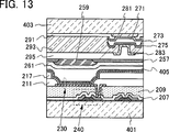
In
Zusätzlich beinhaltet der Bereich mit geringer Flexibilität vorzugsweise eine externe Verbindungselektrode des Licht emittierenden Feldes. Dabei entspricht die externe Verbindungselektrode beispielsweise einer leitenden Schicht
In
Wäre dabei bei der Licht emittierenden Vorrichtung im gefalteten Zustand ein Endabschnitt (auch als gefalteter Abschnitt oder dergleichen bezeichnet) des Licht emittierenden Feldes
Bei der Licht emittierenden Vorrichtung im gefalteten Zustand in
Außerdem ist bei der Licht emittierenden Vorrichtung im gefalteten Zustand in
Folglich ist bei der Licht emittierenden Vorrichtung vorzugsweise die Länge W1 des Bereichs A mit geringer Flexibilität, der die externe Verbindungselektrode überlappt, länger als die Länge W3 des Bereichs B mit geringer Flexibilität, der näher an dem Bereich A ist. Besonders bevorzugt ist unter der Länge W1 des Bereichs A, der Länge W3 des Bereichs B und der Länge W2 eines Bereichs C mit geringer Flexibilität, der weiter entfernt von dem Bereich A ist, W1 am längsten und W2 ist am zweitlängsten.Thus, in the light emitting device, preferably, the length W1 of the low flexibility region A overlapping the external connection electrode is longer than the length W3 of the low flexibility region B closer to the region A. More preferably, among the length W1 of the region A, the length W3 of the region B, and the length W2 of a region C of low flexibility farther away from the region A, W1 is the longest and W2 is the second longest.
Das Trägerteil ist auf der Licht emittierenden Oberflächenseite und/oder der der Licht emittierenden Oberflächenseite entgegengesetzten Seite des Licht emittierenden Feldes angeordnet.The support member is disposed on the light-emitting surface side and / or the light-emitting surface side opposite side of the light-emitting panel.
Das Licht emittierende Feld weist vorzugsweise Trägerteile wie die Trägerteile
Alternativ kann statt der Trägerteile
Beispielsweise liegen in
Das Licht emittierende Feld weist vorzugsweise das Trägerteil entweder auf der Licht emittierenden Oberflächenseite oder auf der der Licht emittierenden Oberflächenseite entgegengesetzten Seite auf, da die Licht emittierende Vorrichtung dünner oder leichter sein kann. Beispielsweise kann eine Licht emittierende Vorrichtung eingesetzt werden, die, wie in
Der Bereich E1 mit hoher Flexibilität und der Bereich E2 mit geringer Flexibilität beinhalten vorzugsweise das Licht emittierende Feld und eine Schutzschicht, die eine höhere Flexibilität aufweist als das Trägerteil und das Licht emittierende Feld überlappt. In diesem Fall kann bei der Licht emittierenden Vorrichtung der Bereich E1 mit hoher Flexibilität eine hohe mechanische Festigkeit sowie eine Flexibilität aufweisen, und es wird weniger wahrscheinlich, dass die Licht emittierende Vorrichtung beschädigt wird. Diese Struktur macht es weniger wahrscheinlich, dass die Licht emittierende Vorrichtung durch eine äußere Kraft oder dergleichen in dem Bereich mit hoher Flexibilität sowie in dem Bereich mit geringer Flexibilität verformt wird und beschädigt wird.The high flexibility region E1 and the low flexibility region E2 preferably include the light emitting field and a protective layer that has higher flexibility than the carrier part and overlaps the light emitting field. In this case, in the light emitting device, the high flexibility region E1 can have high mechanical strength as well have a flexibility, and it is less likely that the light-emitting device is damaged. This structure makes it less likely that the light-emitting device will be deformed and damaged by an external force or the like in the high flexibility region as well as in the low flexibility region.
Zum Beispiel ist unter dem Licht emittierenden Feld, dem Trägerteil und der Schutzschicht vorzugsweise das Trägerteil am dicksten und das Licht emittierende Feld ist am dünnsten. Alternativ weist zum Beispiel unter dem Licht emittierenden Feld, dem Trägerteil und der Schutzschicht vorzugsweise das Trägerteil die geringste Flexibilität auf und das Licht emittierende Feld weist die höchste Flexibilität auf. Eine derartige Struktur erhöht die Differenz zwischen der Flexibilität des Bereichs mit hoher Flexibilität und derjenigen des Bereichs mit geringer Flexibilität. Dementsprechend kann die Licht emittierende Vorrichtung sicher an dem Bereich mit hoher Flexibilität gefaltet werden, so dass verhindert wird, dass der Bereich mit geringer Flexibilität gebogen wird. Folglich kann die Zuverlässigkeit der Licht emittierenden Vorrichtung verbessert werden. Eine derartige Struktur verhindert auch, dass die Licht emittierende Vorrichtung an einem unerwünschten Teil gebogen wird.For example, under the light-emitting panel, the support member and the protective layer, it is preferable that the support member is thickest and the light-emitting panel is thinnest. Alternatively, for example, among the light-emitting panel, the support member and the protective layer, preferably, the support member has the least flexibility, and the light-emitting panel has the highest flexibility. Such a structure increases the difference between the flexibility of the high flexibility region and that of the low flexibility region. Accordingly, the light-emitting device can be securely folded at the region of high flexibility, so that the region with low flexibility is prevented from being bent. Consequently, the reliability of the light-emitting device can be improved. Such a structure also prevents the light-emitting device from being bent at an undesirable part.
Das Licht emittierende Feld weist vorzugsweise Schutzschichten sowohl auf der Licht emittierenden Oberflächenseite als auch auf der der Licht emittierenden Oberflächenseite entgegengesetzten Seite auf, in welchem Falle das Licht emittierende Feld zwischen einem Paar von Schutzschichten liegen kann; dementsprechend weist die Licht emittierende Vorrichtung eine erhöhte mechanische Festigkeit auf, und es wird weniger wahrscheinlich, dass sie beschädigt wird.The light-emitting panel preferably has protective layers on both the light-emitting surface side and the side opposite the light-emitting surface side, in which case the light-emitting panel may be sandwiched between a pair of protective layers; accordingly, the light-emitting device has increased mechanical strength and is less likely to be damaged.
Zum Beispiel sind, wie in
Alternativ ist vorzuziehen, dass, wie in
Das Licht emittierende Feld weist vorzugsweise die Schutzschicht entweder auf der Licht emittierenden Oberflächenseite oder auf der der Licht emittierenden Oberflächenseite entgegengesetzten Seite auf, da die Licht emittierende Vorrichtung dünner oder leichter sein kann. Beispielsweise kann eine Licht emittierende Vorrichtung eingesetzt werden, die die Schutzschicht
Wenn es sich bei der Schutzschicht
Wie in
Bei der Licht emittierenden Vorrichtung einer Ausführungsform der vorliegenden Erfindung ist das Folgende vorzuziehen: Wenn eine Vielzahl von Bereichen mit hoher Flexibilität abwechselnd nach innen und nach außen gebogen wird, erfüllt der kürzeste Abstand L zwischen einer Oberfläche des Licht emittierenden Feldes, die am nächsten an einer Trägerfläche der Licht emittierenden Vorrichtung ist, und einer Oberfläche des Licht emittierenden Feldes, die am weitesten entfernt von der Trägerfläche ist, L < 2(D + T). Dabei repräsentiert D die Summe der Krümmungsradien des Licht emittierenden Feldes in der Vielzahl von Bereichen mit hoher Flexibilität, und T repräsentiert die Dicke des Licht emittierenden Feldes. In diesem Fall kann die Licht emittierende Vorrichtung dünner gemacht werden.In the light emitting device of one embodiment of the present invention, the following is preferable: When a plurality of high flexibility regions are alternately bent inward and outward, the shortest distance L between a surface of the light emitting field closest to one meets Carrier surface of the light-emitting device, and a surface of the light-emitting field, which is farthest from the support surface, L <2 (D + T). Here, D represents the sum of the radii of curvature of the light-emitting field in the plurality of regions of high flexibility, and T represents the thickness of the light-emitting field. In this case, the light-emitting device can be made thinner.
Die Licht emittierende Vorrichtung in
Indem beispielsweise die Dicken der Trägerteile
Dabei ist bei der Licht emittierenden Vorrichtung das Folgende vorzuziehen: Unter den Bereichen mit geringer Flexibilität, die beim Falten der Licht emittierenden Vorrichtung einander überlappen, ist ein Paar von Bereichen mit geringer Flexibilität, die auf der Außenseite positioniert sind, parallel zur Trägerfläche der Licht emittierenden Vorrichtung, und ein Bereich mit geringer Flexibilität, der auf der Innenseite positioniert ist, ist nicht parallel zur Trägerfläche.Here, in the light-emitting device, the following is preferable: Among the low-flexibility regions which overlap each other when the light-emitting device is folded, a pair of low-flexibility regions positioned on the outside are parallel to the surface of the light-emitting ones Device, and a region of low flexibility, which is positioned on the inside, is not parallel to the support surface.
Bei der Licht emittierenden Vorrichtung einer Ausführungsform der vorliegenden Erfindung ist das Folgende vorzuziehen: Wenn einer von zwei benachbarten Bereichen mit hoher Flexibilität nach innen und der andere nach außen gebogen werden, überlappen ein Kreis, dessen Radius dem Krümmungsradius des Licht emittierenden Feldes in dem einen Bereich mit hoher Flexibilität entspricht, und ein Kreis, dessen Radius dem Krümmungsradius des Licht emittierenden Feldes in dem anderen Bereich mit hoher Flexibilität entspricht, einander, indem sie in einer Richtung parallel zu einer Trägerfläche der Licht emittierenden Vorrichtung bewegt werden. In diesem Fall kann die Licht emittierende Vorrichtung dünner gemacht werden.In the light-emitting device of one embodiment of the present invention, the following is preferable: When one of two adjacent regions is bent inward with high flexibility and the other outward, a circle whose radius overlaps the radius of curvature of the light-emitting field in the one region overlaps with high flexibility, and a circle whose radius corresponds to the radius of curvature of the light-emitting panel in the other high flexibility area is moved by being moved in a direction parallel to a support surface of the light-emitting device. In this case, the light-emitting device can be made thinner.
Wie in
Der kürzeste Abstand L3 zwischen einer Oberfläche, die am nächsten an einer Trägerfläche der Licht emittierenden Vorrichtung ist, und einer Oberfläche des Licht emittierenden Feldes in
Die Schutzschicht und das Trägerteil können unter Verwendung von Kunststoff, Gummi, eines Metalls, einer Legierung oder dergleichen ausgebildet werden. Kunststoff, Gummi oder dergleichen wird vorzugsweise verwendet, da er/es eine Schutzschicht oder ein Trägerteil bilden kann, die/das leicht ist und mit geringerer Wahrscheinlichkeit beschädigt wird. Beispielsweise kann man Silikongummi für die Schutzschicht und Edelstahl oder Aluminium für das Trägerteil verwenden.The protective layer and the support member may be formed using plastic, rubber, a metal, an alloy or the like. Plastic, rubber, or the like is preferably used because it can form a protective layer or carrier that is lightweight and less likely to be damaged. For example, one can use silicone rubber for the protective layer and stainless steel or aluminum for the carrier part.
Die Schutzschicht und das Trägerteil werden vorzugsweise unter Verwendung eines Materials mit hoher Festigkeit ausgebildet. In diesem Fall kann eine Licht emittierende Vorrichtung, die eine hohe Stoßbeständigkeit aufweist und mit geringerer Wahrscheinlichkeit beschädigt wird, bereitgestellt werden. Wenn beispielsweise ein organisches Harz, ein dünnes Metallmaterial oder ein dünnes Legierungsmaterial für die Schutzschicht und das Trägerteil verwendet wird, kann die Licht emittierende Vorrichtung leicht sein, und es kann weniger wahrscheinlich sein, dass sie beschädigt wird. Aus einem ähnlichen Grund wird auch ein Substrat des Licht emittierenden Feldes vorzugsweise unter Verwendung eines Materials mit hoher Festigkeit ausgebildet.The protective layer and the support member are preferably formed by using a high-strength material. In this case, a light-emitting device which has high impact resistance and is less likely to be damaged can be provided. For example, when an organic resin, a thin metal material or a thin alloy material is used for the protective layer and the support member, the light-emitting device may be light and less likely to be damaged. For a similar reason, a substrate of the light-emitting panel is also preferably formed by using a high-strength material.
Die Schutzschicht und das Trägerteil auf der Licht emittierenden Oberflächenseite weisen nicht notwendigerweise eine Lichtdurchlässigkeit auf, falls sie nicht den Licht emittierenden Bereich des Licht emittierenden Feldes überlappen. Wenn die Schutzschicht und das Trägerteil auf der Licht emittierenden Oberflächenseite mindestens einen Teil des Licht emittierenden Bereichs überlappen, werden sie vorzugsweise unter Verwendung eines Materials ausgebildet, das Licht durchlässt, das von dem Licht emittierenden Feld emittiert wird. Es gibt keine Beschränkung hinsichtlich der Lichtdurchlässigkeit der Schutzschicht und des Trägerteils auf der der Licht emittierenden Oberflächenseite entgegengesetzten Seite.The protective layer and the support member on the light-emitting surface side do not necessarily have light transmittance unless they are the light-emitting portion of the light overlap the emitting field. When the protective layer and the support member on the light-emitting surface side overlap at least a part of the light-emitting region, they are preferably formed by using a material that transmits light emitted from the light-emitting panel. There is no limitation to the light transmittance of the protective layer and the support member on the side opposite to the light-emitting surface side.
Wenn zwei von der Schutzschicht, dem Trägerteil und dem Licht emittierenden Feld miteinander verbunden werden, können verschiedene Klebstoffe verwendet werden, wobei beispielsweise ein aushärtendes Harz, das bei Raumtemperatur aushärtend ist (z. B. ein zwei Komponenten enthaltendes Harz), ein lichthärtendes Harz, ein wärmehärtendes Harz oder dergleichen verwendet werden kann. Als Alternative kann auch eine Klebefolie verwendet werden. Alternativ können Bestandteile der Licht emittierenden Vorrichtung beispielsweise mit einer Schraube, die zwei oder mehr von der Schutzschicht, dem Trägerteil und dem Licht emittierenden Feld durchdringt, oder mit einem Stift oder einer Klammer, welcher/welche diese hält, fixiert werden.When two of the protective layer, the support member and the light-emitting panel are bonded together, various adhesives may be used, for example, a thermosetting resin which is thermosetting at room temperature (e.g., a two-component resin), a photocuring resin, a thermosetting resin or the like can be used. As an alternative, an adhesive film may also be used. Alternatively, components of the light-emitting device may be fixed, for example, with a screw that penetrates two or more of the protective layer, the support member, and the light-emitting panel, or with a pin or clip that holds them.
Die Licht emittierende Vorrichtung einer Ausführungsform der vorliegenden Erfindung kann verwendet werden, wobei ein Licht emittierendes Feld (ein Licht emittierender Bereich) in zwei oder mehr Bereiche an einem/mehreren gefalteten Abschnitt/en geteilt ist. Zum Beispiel ist es möglich, den Bereich, der beim Falten der Licht emittierenden Vorrichtung verborgen wird, in einen kein Licht emittierenden Zustand und nur den freiliegenden Bereich in einen Licht emittierenden Zustand zu versetzen. Demzufolge kann der Strom verringert werden, der von einem Bereich verbraucht wird, den ein Benutzer nicht verwendet.The light-emitting device of one embodiment of the present invention may be used wherein a light-emitting panel (a light-emitting panel) is divided into two or more areas at one folded portion (s). For example, it is possible to put the area which is hidden when the light-emitting device is folded into a non-light-emitting state and only the exposed area to a light-emitting state. As a result, the power consumed by an area which a user does not use can be reduced.
Die Licht emittierende Vorrichtung einer Ausführungsform der vorliegenden Erfindung kann einen Sensor beinhalten, um zu bestimmen, ob der Bereich mit hoher Flexibilität jeweils gebogen ist oder nicht. Der Sensor kann beispielsweise aus einem Schalter, einem MEMS-Drucksensor, einem Drucksensor oder dergleichen bestehen.The light-emitting device of one embodiment of the present invention may include a sensor for determining whether the high-flexibility region is bent or not. The sensor may for example consist of a switch, a MEMS pressure sensor, a pressure sensor or the like.
Bei den oben beschriebenen Beispielen beinhaltet die Licht emittierende Vorrichtung zwei Bereiche mit hoher Flexibilität; jedoch ist eine Ausführungsform der vorliegenden Erfindung nicht darauf beschränkt. Zum Beispiel beinhaltet, wie in
Beispielsweise ist bei der Licht emittierenden Vorrichtung in
Außerdem ist bei der Licht emittierenden Vorrichtung in
In
Indem beispielsweise die Dicken der Trägerteile
In
Darüber hinaus kann die Licht emittierende Vorrichtung noch dünner gemacht werden, indem, wie in
Beim Falten der Licht emittierenden Vorrichtung müssen ferner die Bereiche mit hoher Flexibilität nicht unbedingt abwechselnd nach innen und nach außen gebogen werden; beispielsweise kann, wie in
Bei der Licht emittierenden Vorrichtung dieser Ausführungsform kann ein Licht emittierendes Feld einmal oder mehrmals gefaltet werden. Der Krümmungsradius in diesem Fall kann beispielsweise größer als oder gleich 1 mm und kleiner als oder gleich 150 mm sein.In the light-emitting device of this embodiment, a light-emitting panel may be folded once or more. The radius of curvature in this case may be, for example, greater than or equal to 1 mm and less than or equal to 150 mm.
Diese Ausführungsform kann gegebenenfalls mit jeder anderen Ausführungsform kombiniert werden.This embodiment may optionally be combined with any other embodiment.
(Ausführungsform 2)(Embodiment 2)
Bei dieser Ausführungsform werden Licht emittierende Felder anhand von
<Konkretes Beispiel 1><Concrete example 1>
Das Licht emittierende Feld in
Die leitende Schicht
Ein Licht emittierendes Element
Die Farbschicht
Das Licht emittierende Feld beinhaltet eine Vielzahl von Transistoren einschließlich des Transistors
Das Licht emittierende Feld des konkreten Beispiels 1 kann auf die folgende Weise hergestellt werden: Die isolierende Schicht
In dem Fall, in dem ein Material mit geringer Wärmebeständigkeit (z. B. Harz) für ein Substrat verwendet wird, ist es schwierig, das Substrat einer hohen Temperatur im Herstellungsprozess auszusetzen. Deswegen gibt es eine Beschränkung hinsichtlich der Bedingungen, unter denen ein Transistor und ein isolierender Film über dem Substrat ausgebildet werden. Ferner wird in dem Fall, in dem ein Material mit hoher Wasserdurchlässigkeit (z. B. Harz) für ein Substrat einer Licht emittierenden Vorrichtung verwendet wird, vorzugsweise ein Film mit geringer Wasserdurchlässigkeit bei einer hohen Temperatur zwischen dem Substrat und einem Licht emittierenden Element ausgebildet. Beim Herstellungsverfahren dieser Ausführungsform können ein Transistor und dergleichen über einem Bildungssubstrat, das eine hohe Wärmebeständigkeit aufweist, ausgebildet werden; demzufolge können ein hochzuverlässiger Transistor und ein isolierender Film mit ausreichend geringer Wasserdurchlässigkeit bei einer hohen Temperatur ausgebildet werden. Danach werden der Transistor und der isolierende Film auf ein Substrat mit geringer Wärmebeständigkeit übertragen, wodurch ein hochzuverlässiges, Licht emittierendes Feld hergestellt werden kann. Auf diese Weise kann einer Ausführungsform der vorliegenden Erfindung entsprechend eine dünne oder/und leichte Licht emittierende Vorrichtung mit hoher Zuverlässigkeit bereitgestellt werden. Die Einzelheiten des Herstellungsverfahrens werden später beschrieben.In the case where a material having low heat resistance (eg, resin) is used for a substrate, it is difficult to expose the substrate to a high temperature in the manufacturing process. Therefore, there is a limitation on the conditions under which a transistor and an insulating film are formed over the substrate. Further, in the case where a high water permeability material (eg, resin) is used for a substrate of a light emitting device, preferably, a low water permeability film is formed at a high temperature between the substrate and a light emitting element. In the manufacturing method of this embodiment, a transistor and the like may be formed over a formation substrate having high heat resistance; Accordingly, a highly reliable transistor and an insulating film having sufficiently low water permeability can be formed at a high temperature. Thereafter, the transistor and the insulating film are transferred to a substrate having low heat resistance, whereby a highly reliable light-emitting panel can be produced. In this way, according to an embodiment of the present invention, a thin and / or light-emitting device with high reliability can be provided. The details of the manufacturing process will be described later.
Das Substrat
Ein Metallmaterial und ein Legierungsmaterial, welche eine hohe Wärmeleitfähigkeit aufweisen, werden bevorzugt, da sie Wärme leicht in das ganze Substrat leiten und somit einen lokalen Temperaturanstieg in dem Licht emittierenden Feld verhindern können. Die Dicke eines Substrats, für das ein Metallmaterial oder ein Legierungsmaterial verwendet wird, ist bevorzugt größer als oder gleich 10 μm und kleiner als oder gleich 200 μm, stärker bevorzugt größer als oder gleich 20 μm und kleiner als oder gleich 50 μm.A metal material and an alloy material having a high thermal conductivity are preferred because they can easily conduct heat into the entire substrate and thus prevent local temperature rise in the light-emitting panel. The thickness of a substrate for which a metal material or an alloy material is used is preferably greater than or equal to 10 μm and less than or equal to 200 μm, more preferably greater than or equal to 20 μm and less than or equal to 50 μm.
Des Weiteren kann dann, wenn ein Material mit hohem Wärmeemissionsgrad für das Substrat
<Konkretes Beispiel 2> <Concrete example 2>
Das Licht emittierende Feld in
Das konkrete Beispiel 2 beinhaltet die isolierende Schicht
Als Licht empfangendes Element, das in dem Licht emittierenden Feld enthalten ist, kann beispielsweise eine PN-Photodiode oder eine PIN-Photodiode verwendet werden. Bei dieser Ausführungsform wird als Licht empfangendes Element eine PIN-Photodiode verwendet, die eine p-Typ-Halbleiterschicht
Es sei angemerkt, dass es sich bei der i-Typ-Halbleiterschicht
Die lichtundurchlässige Schicht
Die leitende Schicht
Vorzugsweise wird ein optischer Berührungssensor zwischen dem Substrat
<Konkretes Beispiel 3><Concrete example 3>
Das Licht emittierende Feld in
<Konkretes Beispiel 4><Concrete example 4>
Das Licht emittierende Feld in
Die leitende Schicht
<Konkretes Beispiel 5><Concrete example 5>
Das Licht emittierende Feld in
Die leitende Schicht
<Konkretes Beispiel 6><Concrete example 6>
Das Licht emittierende Feld in
Das Licht emittierende Element
Die Farbschicht
<Konkretes Beispiel 7><Specific Example 7>
Das Licht emittierende Feld in
Die leitende Schicht
Das Licht emittierende Element
Das Substrat
Die leitende Schicht
Die leitende Schicht
Wenn eine Paste (z. B. Silberpaste) als Material für die leitende Schicht, die elektrisch mit der oberen Elektrode
<Beispiele für Materialien><Examples of materials>
Als Nächstes werden Materialien und dergleichen beschrieben, die für ein Licht emittierendes Feld verwendet werden können. Es sei angemerkt, dass die Beschreibung der Bestandteile, die bereits bei dieser Ausführungsform beschrieben worden sind, weggelassen wird.Next, materials and the like that can be used for a light-emitting panel will be described. It should be noted that the description of the components already described in this embodiment will be omitted.
Die Elementschicht
Die Elementschicht
Die Struktur der Transistoren in dem Licht emittierenden Feld ist nicht besonders beschränkt. Beispielsweise kann ein Forward-Staggered-Transistor oder ein Inverted-Staggered-Transistor verwendet werden. Es kann ein Transistor mit oberem Gate oder ein Transistor mit unterem Gate verwendet werden. Ein Halbleitermaterial, das für die Transistoren verwendet wird, ist nicht besonders beschränkt, und beispielsweise kann Silizium oder Germanium verwendet werden. Alternativ kann auch ein Oxidhalbleiter, der mindestens eines von Indium, Gallium und Zink enthält, wie z. B. ein Metalloxid auf In-Ga-Zn-Basis, verwendet werden.The structure of the transistors in the light-emitting panel is not particularly limited. For example, a forward staggered transistor or an inverted staggered transistor may be used. An upper gate transistor or a lower gate transistor may be used. A semiconductor material used for the transistors is not particularly limited, and for example, silicon or germanium may be used. Alternatively, an oxide semiconductor containing at least one of indium, gallium and zinc, such as. For example, an In-Ga-Zn-based metal oxide can be used.
Es gibt keine besondere Beschränkung hinsichtlich der Kristallinität eines Halbleitermaterials, das für die Transistoren verwendet wird, und man kann einen amorphen Halbleiter oder einen Halbleiter mit Kristallinität (einen mikrokristallinen Halbleiter, einen polykristallinen Halbleiter, einen einkristallinen Halbleiter oder einen Halbleiter, der teilweise Kristallbereiche enthält) verwenden. Vorzugsweise wird ein Halbleiter mit Kristallinität verwendet, in welchem Falle eine Verschlechterung der Transistoreigenschaften unterdrückt werden kann.There is no particular limitation on the crystallinity of a semiconductor material used for the transistors, and there may be an amorphous semiconductor or a semiconductor having crystallinity (a microcrystalline semiconductor, a polycrystalline semiconductor, a monocrystalline semiconductor or a semiconductor partially containing crystal regions). use. Preferably, a semiconductor having crystallinity is used, in which case deterioration of the transistor characteristics can be suppressed.
Das Licht emittierende Element, das in dem Licht emittierenden Feld enthalten ist, beinhaltet ein Paar von Elektroden (die untere Elektrode
Das Licht emittierende Element kann eine Top-Emission-Struktur, eine Bottom-Emission-Struktur oder eine Dual-Emission-Struktur haben. Ein leitender Film, der sichtbares Licht durchlässt, wird als Elektrode verwendet, durch die Licht extrahiert wird. Ein leitender Film, der sichtbares Licht reflektiert, wird vorzugsweise als Elektrode verwendet, durch die kein Licht extrahiert wird.The light-emitting element may have a top-emission structure, a bottom-emission structure, or a dual-emission structure. A conductive film that transmits visible light is used as an electrode by which light is extracted. A conductive film that reflects visible light is preferably used as an electrode by which no light is extracted.
Der leitende Film, der sichtbares Licht durchlässt, kann beispielsweise unter Verwendung von Indiumoxid, Indiumzinnoxid (indium tin oxide, ITO), Indiumzinkoxid, Zinkoxid oder Zinkoxid, dem Gallium zugesetzt ist, ausgebildet werden. Alternativ kann auch ein Film aus einem Metallmaterial, wie z. B. Gold, Silber, Platin, Magnesium, Nickel, Wolfram, Chrom, Molybdän, Eisen, Kobalt, Kupfer, Palladium oder Titan, einer Legierung, die ein beliebiges dieser Metallmaterialien enthält, oder einem Nitrid eines beliebigen dieser Metallmaterialien (z. B. Titannitrid) dünn ausgebildet werden, um eine Lichtdurchlässigkeit aufzuweisen. Alternativ kann auch ein mehrschichtiger Film aus beliebigen der vorstehenden Materialien als leitender Film verwendet werden. Zum Beispiel wird vorzugsweise ein mehrschichtiger Film, der ITO und eine Legierung aus Silber und Magnesium enthält, verwendet, in welchem Falle die Leitfähigkeit erhöht werden kann. Als weitere Alternative kann Graphen oder dergleichen verwendet werden.The conductive film which transmits visible light may be formed, for example, by using indium oxide, indium tin oxide (ITO), indium zinc oxide, zinc oxide or zinc oxide added with gallium. Alternatively, a film of a metal material, such. As gold, silver, platinum, magnesium, nickel, tungsten, chromium, molybdenum, iron, cobalt, copper, palladium or titanium, an alloy containing any of these metal materials, or a nitride of any of these metal materials (eg. Titanium nitride) are made thin to have a light transmittance. Alternatively, a multilayer film of any of the above materials may be used as the conductive film. For example, a multilayer film containing ITO and an alloy of silver and magnesium is preferably used, in which case the conductivity can be increased. As another alternative, graphene or the like can be used.
Für den leitenden Film, der sichtbares Licht reflektiert, kann beispielsweise ein Metallmaterial, wie z. B. Aluminium, Gold, Platin, Silber, Nickel, Wolfram, Chrom, Molybdän, Eisen, Kobalt, Kupfer oder Palladium, oder eine Legierung, die ein beliebiges dieser Metallmaterialien enthält, verwendet werden. Ferner kann Lanthan, Neodym, Germanium oder dergleichen dem Metallmaterial oder der Legierung zugesetzt werden. Zudem kann eine Aluminium enthaltende Legierung (eine Aluminiumlegierung), wie z. B. eine Legierung aus Aluminium und Titan, eine Legierung aus Aluminium und Nickel oder eine Legierung aus Aluminium und Neodym, oder eine Silber enthaltende Legierung, wie z. B. eine Legierung aus Silber und Kupfer, eine Legierung aus Silber, Kupfer und Palladium oder eine Legierung aus Silber und Magnesium, für den leitenden Film verwendet werden. Eine Legierung aus Silber und Kupfer wird aufgrund ihrer hohen Wärmebeständigkeit bevorzugt. Des Weiteren kann dann, wenn ein Metallfilm oder ein Metalloxidfilm auf und in Kontakt mit einem Aluminiumlegierungsfilm angeordnet ist, eine Oxidation des Aluminiumlegierungsfilms verhindert werden. Beispiele für ein Material für den Metallfilm oder den Metalloxidfilm sind Titan und Titanoxid. Alternativ können der vorstehende leitende Film, der sichtbares Licht durchlässt, und ein Film, der ein Metallmaterial enthält, übereinander geschichtet werden. Zum Beispiel kann ein mehrschichtiger Film aus Silber und ITO oder ein mehrschichtiger Film, der eine Legierung aus Silber und Magnesium und ITO enthält, verwendet werden.For the conductive film that reflects visible light, for example, a metal material such. Aluminum, gold, platinum, silver, nickel, tungsten, chromium, molybdenum, iron, cobalt, copper or palladium, or an alloy containing any of these metal materials. Further, lanthanum, neodymium, germanium or the like may be added to the metal material or the alloy. In addition, an aluminum-containing alloy (an aluminum alloy), such as. Example, an alloy of aluminum and titanium, an alloy of aluminum and nickel or an alloy of aluminum and neodymium, or a silver-containing alloy, such. For example, an alloy of silver and copper, an alloy of silver, copper and palladium or an alloy of silver and magnesium may be used for the conductive film. An alloy of silver and copper is preferred because of its high heat resistance. Further, when a metal film or a metal oxide film is disposed on and in contact with an aluminum alloy film, oxidation of the aluminum alloy film can be prevented. Examples of a material for the metal film or the metal oxide film are titanium and titanium oxide. Alternatively, the above conductive film which transmits visible light and a film containing a metallic material may be stacked one upon the other. For example, a multilayer film of silver and ITO or a multilayer film containing an alloy of silver and magnesium and ITO may be used.
Jede der Elektroden kann durch ein Verdampfungsverfahren oder ein Sputterverfahren ausgebildet werden. Alternativ kann auch ein Ausstoßverfahren, wie z. B. ein Tintenstrahlverfahren, ein Druckverfahren, wie z. B. ein Siebdruckverfahren, oder ein Plattierungsverfahren verwendet werden.Each of the electrodes may be formed by an evaporation method or a sputtering method. Alternatively, an ejection method, such. As an ink-jet method, a printing method such. As a screen printing method, or a plating method can be used.
Wenn eine Spannung, die höher ist als die Schwellenspannung des Licht emittierenden Elementes, zwischen der unteren Elektrode
Die EL-Schicht
Für die EL-Schicht
Bei der Elementschicht
Als isolierender Film mit geringer Wasserdurchlässigkeit kann ein Film, der Stickstoff und Silizium enthält (z. B. ein Siliziumnitridfilm oder ein Siliziumnitridoxidfilm), ein Film, der Stickstoff und Aluminium enthält (z. B. ein Aluminiumnitridfilm), oder dergleichen verwendet werden. Als Alternative kann auch ein Siliziumoxidfilm, ein Siliziumoxynitridfilm, ein Aluminiumoxidfilm oder dergleichen verwendet werden.As the insulating film with low water permeability, a film containing nitrogen and silicon (eg, a silicon nitride film or a silicon nitride oxide film), a film containing nitrogen and aluminum (eg, an aluminum nitride film), or the like may be used. Alternatively, a silicon oxide film, a silicon oxynitride film, an alumina film or the like may be used.
Der Wasserdampfdurchlässigkeitsgrad des isolierenden Films mit geringer Wasserdurchlässigkeit ist beispielsweise niedriger als oder gleich 1 × 10⁻⁵ [g/m2·Tag], bevorzugt niedriger als oder gleich 1 × 10⁻⁶ [g/m2·Tag], stärker bevorzugt niedriger als oder gleich 1 × 10⁻⁷ [g/m2·Tag], noch stärker bevorzugt niedriger als oder gleich 1 × 10⁻⁸ [g/m2·Tag].The water vapor transmission rate of the low water permeability insulating film is, for example, lower than or equal to 1 × 10 -5 [g / m 2 · day], preferably lower than or equal to 1 × 10 -6 [g / m 2 · day], more preferably lower greater than or equal to 1 x 10 -7 [g / m 2 .day], even more preferably less than or equal to 1 x 10 -8 [g / m 2 .day].
Das Substrat
Ein organisches Harz, das leichter ist als Glas, wird vorzugsweise für das Substrat
Beispiele für ein Material, das Flexibilität und eine Lichtdurchlässigkeit für sichtbares Licht aufweist, umfassen Glas, das dünn genug ist, um Flexibilität aufzuweisen, Polyesterharze, wie z. B. Polyethylenterephthalat (PET) und Polyethylennaphthalat (PEN), ein Polyacrylnitrilharz, ein Polyimidharz, ein Polymethylmethacrylatharz, ein Polycarbonat-(PC-)Harz, ein Polyethersulfon-(PES-)Harz, ein Polyamidharz, ein Cycloolefinharz, ein Polystyrolharz, ein Polyamidimidharz und ein Polyvinylchloridharz. Im Besonderen wird ein Material bevorzugt, dessen Wärmeausdehnungskoeffizient gering ist, und beispielsweise kann ein Polyamidimidharz, ein Polyimidharz oder PET vorteilhaft verwendet werden. Man kann auch ein Substrat, bei dem eine Glasfaser mit einem organischen Harz imprägniert ist, oder ein Substrat verwenden, dessen Wärmeausdehnungskoeffizient durch Mischen eines organischen Harzes mit einem anorganischen Füllmaterial verringert ist.Examples of a material that has flexibility and visible light transmittance include glass that is thin enough to have flexibility, polyester resins such as polyester resins. Polyethylene terephthalate (PET) and polyethylene naphthalate (PEN), a polyacrylonitrile resin, a polyimide resin, a polymethylmethacrylate resin, a polycarbonate (PC) resin, a polyethersulfone (PES) resin, a polyamide resin, a cycloolefin resin, a polystyrene resin, a polyamideimide resin and a polyvinyl chloride resin. In particular, a material whose thermal expansion coefficient is small is preferable, and for example, a polyamideimide resin, a polyimide resin or PET can be advantageously used. Also, a substrate in which a glass fiber is impregnated with an organic resin or a substrate whose thermal expansion coefficient is reduced by mixing an organic resin with an inorganic filler may be used.
Das Substrat
Die Klebeschicht
Für die Klebeschicht
Außerdem kann das Harz ein Trocknungsmittel enthalten. Beispielsweise kann eine Substanz, die durch eine chemische Adsorption Feuchtigkeit adsorbiert, wie z. B. ein Oxid eines Erdalkalimetalls (z. B. Calciumoxid oder Bariumoxid), verwendet werden. Alternativ kann auch eine Substanz, die durch eine physikalische Adsorption Feuchtigkeit adsorbiert, wie z. B. Zeolith oder Kieselgel, verwendet werden. Das Trocknungsmittel ist vorzugsweise enthalten, da es verhindern kann, dass eine Verunreinigung, wie z. B. Feuchtigkeit, in das Licht emittierende Element eindringt; somit kann die Zuverlässigkeit der Licht emittierenden Vorrichtung verbessert werden.In addition, the resin may contain a drying agent. For example, a substance that is hydrated by a chemical adsorption adsorbed, such. For example, an oxide of an alkaline earth metal (eg, calcium oxide or barium oxide) may be used. Alternatively, a substance which adsorbs moisture by a physical adsorption, such as. As zeolite or silica gel. The desiccant is preferably included since it can prevent contamination such as. Moisture, entering the light-emitting element; thus, the reliability of the light-emitting device can be improved.
Zusätzlich wird vorzugsweise ein Füllmaterial mit einem hohen Brechungsindex (z. B. Titanoxid) in das Harz gemischt, in welchem Falle die Effizienz der Lichtextraktion von dem Licht emittierenden Element verbessert werden kann.In addition, it is preferable to mix a filler having a high refractive index (eg, titanium oxide) in the resin, in which case the efficiency of light extraction from the light-emitting element can be improved.
Die Klebeschicht
Die Differenz zwischen dem Brechungsindex des Harzes und demjenigen der Partikel mit einem Brechungsindex, der sich von demjenigen des Harzes unterscheidet, ist bevorzugt 0,1 oder mehr, stärker bevorzugt 0,3 oder mehr. Insbesondere kann ein Epoxidharz, ein Acrylharz, ein Imidharz, Silikon oder dergleichen als Harz verwendet werden, und als Partikel kann Titanoxid, Bariumoxid, Zeolith oder dergleichen verwendet werden.The difference between the refractive index of the resin and that of the particles having a refractive index different from that of the resin is preferably 0.1 or more, more preferably 0.3 or more. In particular, an epoxy resin, an acrylic resin, an imide resin, silicone or the like may be used as the resin, and as the particle, titanium oxide, barium oxide, zeolite or the like may be used.
Titanoxid- oder Bariumoxidpartikel werden bevorzugt, weil sie Licht sehr gut streuen. Wenn Zeolith verwendet wird, kann er Wasser, das in dem Harz und dergleichen enthalten ist, adsorbieren, wodurch die Zuverlässigkeit des Licht emittierenden Elementes verbessert wird.Titanium oxide or barium oxide particles are preferred because they scatter light very well. When zeolite is used, it can adsorb water contained in the resin and the like, thereby improving the reliability of the light-emitting element.
Die isolierende Schicht
Die isolierende Schicht
Als jede der isolierenden Schichten
Die isolierende Schicht
Als Material für die isolierende Schicht
Es gibt keine besondere Beschränkung hinsichtlich des Verfahrens zum Ausbilden der isolierenden Schicht
Die isolierende Schicht
Die isolierenden Schichten
Für die Dichtungsschicht
Die leitenden Schichten
Beispielsweise kann jede der leitenden Schichten in einer einschichtigen oder mehrschichtigen Struktur ausgebildet werden, bei der ein Metallmaterial, wie z. B. Molybdän, Titan, Chrom, Tantal, Wolfram, Aluminium, Kupfer, Neodym oder Scandium, oder ein Legierungsmaterial, das ein beliebiges dieser Elemente enthält, verwendet wird. Jede der leitenden Schichten kann unter Verwendung eines leitenden Metalloxids ausgebildet werden. Als leitendes Metalloxid kann Indiumoxid (z. B. In2O3), Zinnoxid (z. B. SnO2), Zinkoxid (z. B. ZnO), ITO, Indiumzinkoxid (z. B. In2O3-ZnO) oder ein beliebiges dieser Metalloxidmaterialien, das Siliziumoxid enthält, verwendet werden.For example, each of the conductive layers may be formed in a single-layered or multi-layered structure in which a metal material, such as a metal substrate, may be formed. Molybdenum, titanium, chromium, tantalum, tungsten, aluminum, copper, neodymium or scandium, or an alloy material containing any of these elements. Each of the conductive layers may be formed using a conductive metal oxide. Indium oxide (eg In 2 O 3 ), tin oxide (eg SnO 2 ), zinc oxide (eg ZnO), ITO, indium zinc oxide (eg In 2 O 3 -ZnO) may be used as the conductive metal oxide. or any of these metal oxide materials containing silica may be used.
Die leitenden Schichten
Es handelt sich bei jeder der leitenden Schichten
Als die leitfähigen Partikel
Für den Verbinder
Es handelt sich bei der Farbschicht
Die lichtundurchlässige Schicht
Vorzugsweise ist die isolierende Schicht
<Beispiel für ein Herstellungsverfahren><Example of a manufacturing process>
Als Nächstes wird ein Beispiel für ein Verfahren zum Herstellen eines Licht emittierenden Feldes anhand von
Zunächst wird eine Trennschicht
Außerdem wird eine Trennschicht
Das Bildungssubstrat
Für das Glassubstrat kann beispielsweise ein Glasmaterial, wie z. B. Aluminosilikatglas, Aluminoborosilikatglas oder Bariumborosilikatglas, verwendet werden. Wenn die Temperatur einer später durchgeführten Wärmebehandlung hoch ist, wird vorzugsweise ein Substrat verwendet, das eine untere Entspannungsgrenze (strain point) von 730°C oder höher aufweist.For the glass substrate, for example, a glass material such. As aluminosilicate glass, aluminoborosilicate or barium borosilicate glass, are used. When the temperature of a heat treatment performed later is high, a substrate having a strain point of 730 ° C. or higher is preferably used.
Es sei angemerkt, dass das Glassubstrat wärmebeständig und praktischer sein kann, wenn es eine große Menge an Bariumoxid (BaO) enthält. Alternativ kann auch kristallisiertes Glas oder dergleichen verwendet werden.It should be noted that the glass substrate may be heat-resistant and more practical if it contains a large amount of barium oxide (BaO). Alternatively, crystallized glass or the like may be used.
In dem Fall, in dem ein Glassubstrat als Bildungssubstrat verwendet wird, wird vorzugsweise ein isolierender Film, wie z. B. ein Siliziumoxidfilm, ein Siliziumoxynitridfilm, ein Siliziumnitridfilm oder ein Siliziumnitridoxidfilm, zwischen dem Bildungssubstrat und der Trennschicht ausgebildet, in welchem Falle eine Kontamination durch das Glassubstrat verhindert werden kann.In the case where a glass substrate is used as the forming substrate, it is preferable to use an insulating film such as an insulating film. For example, a silicon oxide film, a silicon oxynitride film, a silicon nitride film or a silicon nitride oxide film is formed between the formation substrate and the separation layer, in which case contamination by the glass substrate can be prevented.
Die Trennschicht
Die Trennschicht kann durch ein Sputterverfahren, ein Plasma-CVD-Verfahren, ein Beschichtungsverfahren, ein Druckverfahren oder dergleichen ausgebildet werden. Es sei angemerkt, dass ein Rotationsbeschichtungsverfahren, ein Tröpfchenausstoßverfahren und ein Dispenserverfahren zum Beschichtungsverfahren gehören.The separation layer may be formed by a sputtering method, a plasma CVD method, a coating method, a printing method, or the like. It should be noted that a spin coating method, a droplet ejecting method, and a dispensing method belong to the coating method.
In dem Fall, in dem die Trennschicht eine einschichtige Struktur hat, wird vorzugsweise eine Wolframschicht, eine Molybdänschicht oder eine Schicht, die eine Mischung aus Wolfram und Molybdän enthält, ausgebildet. Alternativ kann auch eine Schicht, die ein Oxid oder ein Oxynitrid von Wolfram enthält, eine Schicht, die ein Oxid oder ein Oxynitrid von Molybdän enthält, oder eine Schicht, die ein Oxid oder ein Oxynitrid einer Mischung aus Wolfram und Molybdän enthält, ausgebildet werden. Es sei angemerkt, dass die Mischung aus Wolfram und Molybdän beispielsweise einer Legierung aus Wolfram und Molybdän entspricht.In the case where the separation layer has a single-layer structure, it is preferable to use a tungsten layer, a molybdenum layer or a layer. which contains a mixture of tungsten and molybdenum. Alternatively, a layer containing an oxide or an oxynitride of tungsten, a layer containing an oxide or an oxynitride of molybdenum, or a layer containing an oxide or an oxynitride of a mixture of tungsten and molybdenum may also be formed. It should be noted that the mixture of tungsten and molybdenum corresponds, for example, to an alloy of tungsten and molybdenum.
In dem Fall, in dem die Trennschicht in einer mehrschichtigen Struktur ausgebildet wird, die eine Wolfram enthaltende Schicht und eine ein Oxid von Wolfram enthaltende Schicht umfasst, kann die ein Oxid von Wolfram enthaltende Schicht wie folgt ausgebildet werden: Zuerst wird die Wolfram enthaltende Schicht ausgebildet, und ein isolierender Film aus einem Oxid wird darüber ausgebildet, so dass die ein Oxid von Wolfram enthaltende Schicht an der Grenzfläche zwischen der Wolframschicht und dem isolierenden Film ausgebildet wird. Alternativ kann die ein Oxid von Wolfram enthaltende Schicht ausgebildet werden, indem eine thermische Oxidationsbehandlung, eine Sauerstoffplasmabehandlung, eine Distickstoffoxid-(N2O-)Plasmabehandlung, eine Behandlung mit einer stark oxidierenden Lösung, wie z. B. Ozonwasser, oder dergleichen, an der Oberfläche der Wolfram enthaltenden Schicht durchgeführt wird. Eine Plasmabehandlung oder eine Wärmebehandlung kann in einer Atmosphäre von Sauerstoff, Stickstoff oder Distickstoffoxid selbst oder in einem Gasgemisch aus einem beliebigen dieser Gase und einem weiteren Gas durchgeführt werden. Der Oberflächenzustand der Trennschicht wird durch die Plasmabehandlung oder die Wärmebehandlung verändert, wodurch die Adhäsion zwischen der Trennschicht und der später ausgebildeten isolierenden Schicht gesteuert werden kann.In the case where the separation layer is formed in a multilayered structure comprising a tungsten-containing layer and a tungsten-containing layer, the layer containing an oxide of tungsten may be formed as follows: First, the tungsten-containing layer is formed and an insulating film of an oxide is formed over it, so that the layer containing an oxide of tungsten is formed at the interface between the tungsten layer and the insulating film. Alternatively, the layer containing an oxide of tungsten can be formed by subjecting a thermal oxidation treatment, an oxygen plasma treatment, a nitrous oxide (N 2 O) plasma treatment, a treatment with a strongly oxidizing solution, such as e.g. Ozone water, or the like, is carried out on the surface of the tungsten-containing layer. A plasma treatment or a heat treatment may be carried out in an atmosphere of oxygen, nitrogen or nitrous oxide itself or in a gas mixture of any of these gases and another gas. The surface state of the separation layer is changed by the plasma treatment or the heat treatment, whereby the adhesion between the separation layer and the later-formed insulating layer can be controlled.
Jede der isolierenden Schichten kann durch ein Sputterverfahren, ein Plasma-CVD-Verfahren, ein Beschichtungsverfahren, ein Druckverfahren oder dergleichen ausgebildet werden. Zum Beispiel wird die isolierende Schicht durch ein Plasma-CVD-Verfahren bei einer Temperatur von höher als oder gleich 250°C und niedriger als oder gleich 400°C ausgebildet, wodurch es sich bei der isolierenden Schicht um einen dichten Film mit sehr geringer Wasserdurchlässigkeit handeln kann.Each of the insulating layers may be formed by a sputtering method, a plasma CVD method, a coating method, a printing method, or the like. For example, the insulating layer is formed by a plasma CVD method at a temperature higher than or equal to 250 ° C and lower than or equal to 400 ° C, whereby the insulating layer is a dense film having a very low water permeability can.
Danach wird ein Material für die Dichtungsschicht
Anschließend wird das Bildungssubstrat
Verschiedene Verfahren können gegebenenfalls für den Trennungsprozess verwendet werden. Wenn beispielsweise eine Schicht, die einen Metalloxidfilm umfasst, als Trennschicht auf der Seite in Kontakt mit der abzutrennenden Schicht ausgebildet wird, wird der Metalloxidfilm durch Kristallisation brüchig, wodurch die abzutrennende Schicht von dem Bildungssubstrat abgetrennt werden kann. Alternativ wird dann, wenn ein Wasserstoff enthaltender amorpher Siliziumfilm als Trennschicht zwischen dem Bildungssubstrat, das eine hohe Wärmebeständigkeit aufweist, und der abzutrennenden Schicht ausgebildet wird, der amorphe Siliziumfilm durch eine Bestrahlung mit Laserlicht oder ein Ätzen entfernt, wodurch die abzutrennende Schicht von dem Bildungssubstrat abgetrennt werden kann. Alternativ wird, nachdem eine Schicht, die einen Metalloxidfilm umfasst, als Trennschicht auf der Seite in Kontakt mit der abzutrennenden Schicht ausgebildet worden ist, der Metalloxidfilm durch Kristallisation brüchig, und ein Teil der Trennschicht wird durch ein Ätzen unter Verwendung einer Lösung oder eines Fluoridgases, wie z. B. NF3, BrF3 oder ClF3, entfernt, wodurch die Trennung an dem brüchigen Metalloxidfilm auftreten kann. Ferner kann ein Verfahren verwendet werden, bei dem ein Film, der Stickstoff, Sauerstoff, Wasserstoff oder dergleichen enthält (zum Beispiel ein Wasserstoff enthaltender amorpher Siliziumfilm, ein Wasserstoff enthaltender Legierungsfilm, ein Sauerstoff enthaltender Legierungsfilm oder dergleichen), als Trennschicht verwendet wird und bei dem die Trennschicht mit Laserlicht bestrahlt wird, um den in der Trennschicht enthaltenen Stickstoff, Sauerstoff oder Wasserstoff als Gas abzugeben, wodurch die Trennung zwischen der abzutrennenden Schicht und dem Bildungssubstrat gefördert wird. Alternativ ist es auch möglich, ein Verfahren, bei dem das Bildungssubstrat, das mit der abzutrennenden Schicht versehen ist, mechanisch oder durch ein Ätzen unter Verwendung einer Lösung oder eines Fluoridgases, wie z. B. NF3, BrF3 oder ClF3, entfernt wird, oder dergleichen zu verwenden. In diesem Fall wird die Trennschicht nicht notwendigerweise bereitgestellt.Various methods may optionally be used for the separation process. For example, when a layer comprising a metal oxide film is formed as a release layer on the side in contact with the layer to be separated, the metal oxide film becomes brittle by crystallization, whereby the layer to be separated can be separated from the formation substrate. Alternatively, when a hydrogen-containing amorphous silicon film is formed as a separation layer between the formation substrate having high heat resistance and the layer to be separated, the amorphous silicon film is removed by irradiation with laser light or etching, whereby the layer to be separated is separated from the formation substrate can be. Alternatively, after a layer comprising a metal oxide film has been formed as a release layer on the side in contact with the layer to be separated, the metal oxide film becomes brittle by crystallization, and a part of the separation layer is removed by etching using a solution or a fluoride gas. such as As NF 3 , BrF 3 or ClF 3 , removed, whereby the separation of the brittle metal oxide film can occur. Further, a method may be used in which a film containing nitrogen, oxygen, hydrogen or the like (for example, a hydrogen-containing amorphous silicon film, a hydrogen-containing alloy film, an alloy-containing alloy film or the like) is used as the release layer and in which the separation layer is irradiated with laser light to release the nitrogen, oxygen or hydrogen contained in the separation layer as a gas, whereby the separation between the layer to be separated and the formation substrate is promoted. Alternatively, it is also possible to use a method in which the formation substrate provided with the layer to be separated is formed mechanically or by etching using a solution or a fluoride gas such as fluoride gas. B. NF 3 , BrF 3 or ClF 3 , or the like to use. In this case, the separation layer is not necessarily provided.
Überdies kann der Trennungsprozess durch Kombination der oben beschriebenen Trennverfahren leicht ausgeführt werden. Mit anderen Worten: Die Trennung kann mit physikalischer Kraft (durch eine Maschine oder dergleichen) durchgeführt werden, nachdem die Trennschicht einer Bestrahlung mit Laserlicht, einem Ätzen mit einem Gas, einer Lösung oder dergleichen oder einer mechanischen Entfernung mit einem scharfen Messer, Skalpell oder dergleichen unterzogen worden ist, so dass die Trennschicht und die abzutrennende Schicht leicht voneinander abgetrennt werden können.Moreover, the separation process can be achieved by combining the above-described Separation method can be easily performed. In other words, the separation can be performed with physical force (by a machine or the like) after the separation layer is irradiated with laser light, etching with a gas, solution or the like or mechanical removal with a sharp knife, scalpel or the like has been subjected, so that the release layer and the separated layer can be easily separated from each other.
Die Trennung der abzutrennenden Schicht von dem Bildungssubstrat kann ausgeführt werden, indem die Grenzfläche zwischen der Trennschicht und der abzutrennenden Schicht mit einer Flüssigkeit gefüllt wird. Ferner kann die Trennung ausgeführt werden, während eine Flüssigkeit, wie z. B. Wasser, gegossen wird.The separation of the layer to be separated from the formation substrate may be carried out by filling the interface between the separation layer and the layer to be separated with a liquid. Furthermore, the separation can be carried out while a liquid, such. As water is poured.
Als weiteres Trennverfahren wird vorzugsweise in dem Fall, in dem die Trennschicht unter Verwendung von Wolfram ausgebildet wird, die Trennung durchgeführt, während die Trennschicht unter Verwendung eines Lösungsgemisches aus Ammoniakwasser und einer Wasserstoffperoxidlösung geätzt wird.As another separation method, preferably, in the case where the separation layer is formed by using tungsten, the separation is performed while the separation layer is etched using a mixed solution of ammonia water and a hydrogen peroxide solution.
Es sei angemerkt, dass die Trennschicht nicht notwendig ist, falls die Trennung an der Grenzfläche zwischen dem Bildungssubstrat und der abzutrennenden Schicht möglich ist. Zum Beispiel wird Glas als Bildungssubstrat verwendet, ein organisches Harz, wie z. B. Polyimid, Polyester, Polyolefin, Polyamid, Polycarbonat oder Acryl, wird in Kontakt mit dem Glas ausgebildet, und ein isolierender Film, ein Transistor und dergleichen werden über dem organischen Harz ausgebildet. In diesem Fall erfolgt durch eine Erwärmung des organischen Harzes die Trennung an der Grenzfläche zwischen dem Bildungssubstrat und dem organischen Harz. Alternativ kann auch eine Trennung an der Grenzfläche zwischen einer Metallschicht und dem organischen Harz auf die folgende Weise durchgeführt werden: Die Metallschicht wird zwischen dem Bildungssubstrat und dem organischen Harz angeordnet, und ein Strom wird zum Fließen in der Metallschicht gebracht, so dass die Metallschicht erwärmt wird. Das organische Harz, das von dem Bildungssubstrat abgetrennt worden ist, kann als Substrat des Licht emittierenden Feldes verwendet werden. Alternativ kann das organische Harz mit einem Klebstoff an einem Substrat angebracht werden.It should be noted that the separation layer is not necessary if the separation is possible at the interface between the formation substrate and the layer to be separated. For example, glass is used as a formation substrate, an organic resin such as, for example, an organic resin. Polyimide, polyester, polyolefin, polyamide, polycarbonate or acrylic, is formed in contact with the glass, and an insulating film, a transistor and the like are formed over the organic resin. In this case, by heating the organic resin, the separation occurs at the interface between the formation substrate and the organic resin. Alternatively, a separation at the interface between a metal layer and the organic resin may be performed in the following manner: The metal layer is disposed between the formation substrate and the organic resin, and a current is caused to flow in the metal layer, so that the metal layer is heated becomes. The organic resin which has been separated from the formation substrate can be used as a substrate of the light-emitting panel. Alternatively, the organic resin may be attached to a substrate with an adhesive.
Schließlich wird eine Öffnung in der isolierenden Schicht
Auf die oben beschriebene Weise kann das Licht emittierende Feld hergestellt werden.In the manner described above, the light-emitting panel can be manufactured.
Wie oben beschrieben, beinhaltet das Licht emittierende Feld dieser Ausführungsform zwei Substrate; eines ist das Substrat
Diese Ausführungsform kann gegebenenfalls mit jeder anderen Ausführungsform kombiniert werden.This embodiment may optionally be combined with any other embodiment.
(Ausführungsform 3)(Embodiment 3)
Bei dieser Ausführungsform wird ein Licht emittierendes Feld anhand von
Das Licht emittierende Feld in
Das Licht emittierende Feld beinhaltet eine Klebeschicht (nicht gezeigt), die in Rahmenform zwischen dem Substrat
Bei dem Licht emittierenden Feld dieser Ausführungsform weist das Substrat
Das Licht emittierende Feld dieser Ausführungsform ist zur Touch-Bedienung geeignet. Mit dem Licht empfangenden Element kann insbesondere eine Nähe oder ein Kontakt eines Objekts an einer Oberfläche des Substrats
Ein optischer Berührungssensor ist sehr haltbar und wird bevorzugt, weil seine Erfassungsgenauigkeit nicht durch Schäden an einer Oberfläche, die von einem Objekt berührt wird, beeinflusst wird. Ein optischer Berührungssensor hat auch Vorteile, dass er zur kontaktlosen Erfassung geeignet ist, dass er die Bildschärfe nicht verschlechtert, wenn er bei einer Anzeigevorrichtung verwendet wird und dass er für große Licht emittierende Felder und Anzeigevorrichtungen eingesetzt werden kann.An optical touch sensor is very durable and is preferred because its detection accuracy is not affected by damage to a surface touched by an object. An optical touch sensor also has advantages that it is suitable for non-contact detection, that it does not deteriorate the image sharpness when used in a display device, and that it can be used for large light-emitting panels and display devices.
Vorzugsweise wird ein optischer Berührungssensor zwischen dem Substrat
Die lichtundurchlässige Schicht
Es gibt keine besondere Beschränkung hinsichtlich der Materialien, die für die Substrate
Es besteht keine Beschränkung hinsichtlich eines Verfahrens zum Abdichten des Licht emittierenden Feldes, und entweder Massivdichtung oder Hohldichtung kann zum Einsatz kommen. Beispielsweise kann als Dichtungsmaterial ein Glasmaterial, wie z. B. eine Glasfritte, oder ein Harzmaterial, wie z. B. ein Harz, das bei Raumtemperatur aushärtend ist (z. B. ein zwei Komponenten enthaltendes Harz), ein lichthärtendes Harz oder ein wärmehärtendes Harz, verwendet werden. Der Raum
Diese Ausführungsform kann gegebenenfalls mit jeder anderen Ausführungsform kombiniert werden.This embodiment may optionally be combined with any other embodiment.
[Beispiel][Example]
Bei diesem Beispiel wurde eine Licht emittierende Vorrichtung einer Ausführungsform der vorliegenden Erfindung hergestellt. Die Licht emittierende Vorrichtung dieses Beispiels kann als eine Anzeige mit dreifach faltbarem Bildschirm (tri-fold folding screen type display) bezeichnet werden.In this example, a light-emitting device of one embodiment of the present invention was fabricated. The light-emitting device of this example may be referred to as a tri-fold folding screen type display.
Das Licht emittierende Feld wurde mittels des bei der Ausführungsform 2 beschriebenen Herstellungsverfahrens hergestellt.The light-emitting panel was produced by the manufacturing method described in
Zunächst wurde die Trennschicht
Wie bei jeder der Trennschichten
Bei der mehrschichtigen Struktur der Trennschicht tritt die Trennung gleich nach der Abscheidung nicht leicht auf; jedoch verändert eine durch eine Wärmebehandlung hervorgerufene Reaktion mit einem anorganischen isolierenden Film den Zustand der Grenzfläche zwischen der Trennschicht und dem anorganischen isolierenden Film, so dass sie brüchig wird. Dann erfolgt eine physikalische Trennung, indem ein Anfangspunkt der Trennung ausgebildet wird.In the multi-layered structure of the separation layer, the separation does not easily occur just after the deposition; however, a reaction with an inorganic insulating film caused by a heat treatment changes the state of the interface between the release layer and the inorganic insulating film to become brittle. Then, a physical separation is made by forming a starting point of the separation.
Als abzutrennende Schicht über der Trennschicht
Eine mehrschichtige Struktur, die einen Siliziumoxynitridfilm, einen Siliziumnitridfilm und dergleichen umfasste, wurde als jede der isolierenden Schichten
Als Transistor wurde ein Transistor verwendet, der einen kristallinen Oxidhalbleiter mit Ausrichtung bezüglich der c-Achse (c-axis aligned crystalline oxide semiconductor, CAAC-OS) enthielt. Da der CAAC-OS, der nicht amorph ist, wenige Defektzustände aufweist, kann die Verwendung des CAAC-OS die Zuverlässigkeit des Transistors verbessern. Da der CAAC-OS keine Korngrenze aufweist, erzeugt außerdem eine Beanspruchung, die durch Biegung einer flexiblen Vorrichtung verursacht wird, nicht leicht einen Riss in einem CAAC-OS-Film.As the transistor, a transistor including a c-axis aligned crystalline oxide semiconductor (CAAC-OS) crystalline oxide semiconductor was used. Since the CAAC-OS, which is not amorphous, has few defect states, the use of the CAAC-OS can improve the reliability of the transistor. In addition, since the CAAC-OS has no grain boundary, stress caused by bending a flexible device does not easily create a crack in a CAAC-OS film.
Es handelt sich bei einem CAAC-OS um einen Oxidhalbleiter, der eine Ausrichtung bezüglich der c-Achse in einer Richtung im Wesentlichen senkrecht zur Filmoberfläche aufweist. Es ist festgestellt worden, dass Oxidhalbleiter, neben einer amorphen Struktur und einer einkristallinen Struktur, verschiedene Kristallstrukturen haben. Ein Beispiel für derartige Strukturen ist eine nanokristalline(nano-crystal, nc-)Struktur, die ein Aggregat von Mikrokristallen im Nanobereich ist. Die Kristallinität einer CAAC-Struktur ist niedriger als diejenige einer einkristallinen Struktur, aber höher als diejenige einer amorphen Struktur und diejenige einer nc-Struktur.A CAAC-OS is an oxide semiconductor that has alignment with the c-axis in a direction substantially perpendicular to the film surface. It has been found that oxide semiconductors, apart from an amorphous structure and a monocrystalline structure, have different crystal structures. An example of such structures is a nanocrystalline (nano-crystal, nc) structure, which is an aggregate of nanocrystalline microcrystals. The crystallinity of a CAAC structure is lower than that of a monocrystalline structure but higher than that of an amorphous structure and that of an nc structure.
Bei diesem Beispiel wurde ein kanalgeätzter Transistor (channel-etched transistor) verwendet, der ein Oxid auf In-Ga-Zn-Basis enthielt. Der Transistor kann bei einer Prozesstemperatur von niedriger als 500°C über einem Glassubstrat hergestellt werden.In this example, a channel-etched transistor was used which contained an In-Ga-Zn-based oxide. The transistor can be fabricated at a process temperature lower than 500 ° C over a glass substrate.
Bei einem Verfahren zum Herstellen eines Elementes, wie z. B. eines Transistors, direkt über einem organischen Harz, wie z. B. einem Kunststoffsubstrat, muss die Temperatur im Prozess zum Herstellen des Elementes niedriger sein als die obere Temperaturgrenze des organischen Harzes. Bei dem Bildungssubstrat dieses Beispiels handelt es sich um ein Glassubstrat, und die Trennschicht, die ein anorganischer Film ist, weist eine hohe Wärmebeständigkeit auf; deshalb kann der Transistor bei einer Temperatur hergestellt werden, die gleich der Temperatur ist, bei der ein Transistor über einem Glassubstrat hergestellt wird. Daher können die Leistung und Zuverlässigkeit des Transistors leicht sichergestellt werden.In a method for producing an element, such. B. a transistor, directly over an organic resin such. As a plastic substrate, the temperature in the process for producing the element must be lower than the upper temperature limit of the organic resin. The formation substrate of this example is a glass substrate, and the release layer, which is an inorganic film, has high heat resistance; therefore, the transistor can be made at a temperature equal to the temperature at which a transistor is fabricated over a glass substrate. Therefore, the performance and reliability of the transistor can be easily ensured.
Als das Licht emittierende Element
Bei dem hergestellten Licht emittierenden Feld hatte ein Licht emittierender Bereich (Pixelabschnitt) eine Größe von 5,9 Zoll in der Diagonale, und es betrugen die Anzahl von Pixeln 720×1280×3 (RGB), der Pixelabstand 0,102 mm×0,102 mm, die Auflösung 249 ppi und das Öffnungsverhältnis 45,2%. Verwendet wurden ein integrierter Abtasttreiber (built-in scan driver) und ein externer Source-Treiber, der durch Chip-on-Film (COF) angebracht wurde.In the manufactured light emitting panel, a light emitting area (pixel portion) had a size of 5.9 inches in the diagonal, and the number of pixels was 720 × 1280 × 3 (RGB), the pixel pitch 0.102 mm × 0.102 mm Resolution 249 ppi and the aperture ratio 45.2%. We used a built-in scan driver and an external source driver mounted by chip-on-film (COF).
Wäre dabei das Licht emittierende Feld mit einem Paar von Schutzschichten und/oder einem Paar von Trägerteilen vollständig fixiert, so würde das Licht emittierende Feld in einigen Fällen beim Falten der Licht emittierenden Vorrichtung unter Spannung beschädigt werden. Beim Öffnen der Licht emittierenden Vorrichtung würde sich außerdem das Licht emittierende Feld in einigen Fällen durch eine Kraft in einer Richtung zusammenziehen, so dass es beschädigt werden würde. Das Licht emittierende Feld der bei diesem Beispiel hergestellten Licht emittierenden Vorrichtung ist mit einem Paar von Schutzschichten und/oder einem Paar von Trägerteilen nicht vollständig fixiert. Dementsprechend verschiebt sich das Licht emittierende Feld beim Falten oder Öffnen der Licht emittierenden Vorrichtung derart, dass sich die Position des Licht emittierenden Feldes in Bezug auf das Paar von Schutzschichten und/oder das Paar von Trägerteilen verändert. Folglich kann verhindert werden, dass das Licht emittierende Feld durch eine Kraft beschädigt wird.In this case, if the light-emitting panel were completely fixed with a pair of protective layers and / or a pair of support members, the light-emitting panel would be damaged in tension when the light-emitting device is folded in some cases. In addition, when opening the light emitting device, the light emitting field would in some cases contract by a force in one direction, so that it would be damaged. The light-emitting panel of the light-emitting device manufactured in this example is not completely fixed with a pair of protective layers and / or a pair of support members. Accordingly, when the light-emitting device is folded or opened, the light-emitting panel shifts so that the position of the light-emitting panel changes with respect to the pair of protective layers and / or the pair of support members. Consequently, the light-emitting panel can be prevented from being damaged by a force.
Die Anzeige auf dem Licht emittierenden Feld
Erläuterung der BezugszeichenExplanation of the reference numbers
-
11 : Licht emittierendes Feld,11a : Licht emittierender Bereich,11b : kein Licht emittierender Bereich,13 : Schutzschicht,13a : Schutzschicht,13b : Schutzschicht,15 : Trägerteil,15a : Trägerteil,15b : Trägerteil,101 : Elementschicht,103 : Substrat,104 : Lichtextraktionsabschnitt,105 : Klebeschicht,106 : Treiberschaltungsabschnitt,108 : FPC,108a : FPC,108b : FPC,156 : leitende Schicht,157 : leitende Schicht,201 : Substrat,202 : Substrat,203 : Klebeschicht,205 : isolierende Schicht,207 : isolierende Schicht,208 : leitende Schicht,209 : isolierende Schicht,209a : isolierende Schicht,209b : isolierende Schicht,211 : isolierende Schicht,212 : leitende Schicht,213 : Dichtungsschicht,215 : Verbinder,215a : Verbinder,215b : Verbinder,217 : isolierende Schicht,230 : Licht emittierendes Element,231 : untere Elektrode,233 : EL-Schicht,235 : obere Elektrode,240 : Transistor,255 : isolierende Schicht,257 : lichtundurchlässige Schicht,259 : Farbschicht,261 : isolierende Schicht,270 : leitende Schicht,271 : p-Typ-Halbleiterschicht,272 : leitende Schicht,273 : i-Typ-Halbleiterschicht,274 : leitende Schicht,275 : n-Typ-Halbleiterschicht,276 : isolierende Schicht,278 : isolierende Schicht,280 : leitende Schicht,281 : leitende Schicht,283 : leitende Schicht,291 : isolierende Schicht,292 : leitfähige Partikel,293 : isolierende Schicht,294 : leitende Schicht,295 : isolierende Schicht,296 : leitende Schicht,301 : Bildungssubstrat,303 : Trennschicht,305 : Bildungssubstrat,307 : Trennschicht,310a : leitende Schicht,310b : leitende Schicht,401 : Substrat,403 : Substrat,405 : Raum.11 : Light emitting field,11a : Light emitting area,11b : no light emitting area,13 : Protective layer,13a : Protective layer,13b : Protective layer,15 : Carrier part,15a : Carrier part,15b : Carrier part,101 : Element layer,103 : Substrate,104 : Light extraction section,105 : Adhesive layer,106 : Driver circuit section,108 : FPC,108a : FPC,108b : FPC,156 : conductive layer,157 : conductive layer,201 : Substrate,202 : Substrate,203 : Adhesive layer,205 : insulating layer,207 : insulating layer,208 : conductive layer,209 : insulating layer,209a : insulating layer,209b : insulating layer,211 : insulating layer,212 : conductive layer,213 : Sealing layer,215 : Interconnects,215a : Interconnects,215b : Interconnects,217 : insulating layer,230 : Light emitting element,231 : lower electrode,233 Photos: EL layer,235 : upper electrode,240 : Transistor,255 : insulating layer,257 : opaque layer,259 : Color layer,261 : insulating layer,270 : conductive layer,271 : p-type semiconductor layer,272 : conductive layer,273 : i-type semiconductor layer,274 : conductive layer,275 : n-type semiconductor layer,276 : insulating layer,278 : insulating layer,280 : conductive layer,281 : conductive layer,283 : conductive layer,291 : insulating layer,292 : conductive particles,293 : insulating layer,294 : conductive layer,295 : insulating layer,296 : conductive layer,301 Image: Education substrate,303 : Separating layer,305 Image: Education substrate,307 : Separating layer,310a : conductive layer,310b : conductive layer,401 : Substrate,403 : Substrate,405 : Room.
Diese Anmeldung basiert auf der
Claims (25)
Applications Claiming Priority (7)
| Application Number | Priority Date | Filing Date | Title |
|---|---|---|---|
| JP2013-146293 | 2013-07-12 | ||
| JP2013146291 | 2013-07-12 | ||
| JP2013-146291 | 2013-07-12 | ||
| JP2013146293 | 2013-07-12 | ||
| JP2013249155 | 2013-12-02 | ||
| JP2013-249155 | 2013-12-02 | ||
| PCT/JP2014/067853 WO2015005230A1 (en) | 2013-07-12 | 2014-06-27 | Light-emitting device |
Publications (1)
| Publication Number | Publication Date |
|---|---|
| DE112014003233T5 true DE112014003233T5 (en) | 2016-04-21 |
Family
ID=52276957
Family Applications (1)
| Application Number | Title | Priority Date | Filing Date |
|---|---|---|---|
| DE112014003233.6T Ceased DE112014003233T5 (en) | 2013-07-12 | 2014-06-27 | Light emitting device |
Country Status (7)
| Country | Link |
|---|---|
| US (10) | US9719665B2 (en) |
| JP (11) | JP6463915B2 (en) |
| KR (6) | KR20260009401A (en) |
| CN (2) | CN108615744A (en) |
| DE (1) | DE112014003233T5 (en) |
| TW (8) | TWI844396B (en) |
| WO (1) | WO2015005230A1 (en) |
Families Citing this family (74)
| Publication number | Priority date | Publication date | Assignee | Title |
|---|---|---|---|---|
| KR102398137B1 (en) | 2013-07-02 | 2022-05-17 | 가부시키가이샤 한도오따이 에네루기 켄큐쇼 | Data processing device |
| TWI667644B (en) | 2013-07-19 | 2019-08-01 | 日商半導體能源研究所股份有限公司 | Data processing device |
| KR20220025259A (en) | 2013-07-19 | 2022-03-03 | 가부시키가이샤 한도오따이 에네루기 켄큐쇼 | Semiconductor device |
| US9395070B2 (en) | 2013-07-19 | 2016-07-19 | Semiconductor Energy Laboratory Co., Ltd. | Support of flexible component and light-emitting device |
| US9356049B2 (en) | 2013-07-26 | 2016-05-31 | Semiconductor Energy Laboratory Co., Ltd. | Display device with a transistor on an outer side of a bent portion |
| US9377817B2 (en) | 2013-08-20 | 2016-06-28 | Semiconductor Energy Laboratory Co., Ltd. | Display device |
| US9229481B2 (en) | 2013-12-20 | 2016-01-05 | Semiconductor Energy Laboratory Co., Ltd. | Semiconductor device |
| KR102358935B1 (en) | 2014-02-12 | 2022-02-04 | 가부시키가이샤 한도오따이 에네루기 켄큐쇼 | Electronic device |
| TWI654736B (en) | 2014-02-14 | 2019-03-21 | Semiconductor Energy Laboratory Co., Ltd. | Illuminating device |
| US9588549B2 (en) | 2014-02-28 | 2017-03-07 | Semiconductor Energy Laboratory Co., Ltd. | Electronic device |
| KR102293958B1 (en) | 2014-02-28 | 2021-08-27 | 가부시키가이샤 한도오따이 에네루기 켄큐쇼 | Electronic device |
| WO2015166376A1 (en) | 2014-05-02 | 2015-11-05 | Semiconductor Energy Laboratory Co., Ltd. | Display device and input/output device |
| KR20210068638A (en) | 2014-10-28 | 2021-06-09 | 가부시키가이샤 한도오따이 에네루기 켄큐쇼 | Light-emitting device |
| KR102298367B1 (en) * | 2015-01-05 | 2021-09-06 | 삼성디스플레이 주식회사 | Display device |
| KR102417119B1 (en) * | 2015-02-11 | 2022-07-06 | 삼성디스플레이 주식회사 | Flexible display device |
| KR102273053B1 (en) | 2015-02-16 | 2021-07-06 | 삼성디스플레이 주식회사 | Display apparatus |
| CN104733503B (en) * | 2015-03-17 | 2018-05-08 | 京东方科技集团股份有限公司 | A kind of display panel and curved face display panel |
| USD789925S1 (en) * | 2015-06-26 | 2017-06-20 | Intel Corporation | Electronic device with foldable display panels |
| JP6850587B2 (en) * | 2015-11-18 | 2021-03-31 | 株式会社半導体エネルギー研究所 | Electronics |
| JP6412036B2 (en) | 2015-12-21 | 2018-10-24 | 株式会社ジャパンディスプレイ | Display device |
| US9837475B2 (en) * | 2015-12-21 | 2017-12-05 | Japan Display Inc. | Display device |
| KR102505585B1 (en) * | 2015-12-31 | 2023-03-02 | 엘지디스플레이 주식회사 | Organic light emitting display panel and organic light emitting display device |
| KR102458892B1 (en) * | 2016-04-27 | 2022-10-26 | 삼성디스플레이 주식회사 | Flexible display device and method of manufacturing the same |
| JP6918560B2 (en) * | 2016-04-28 | 2021-08-11 | 株式会社半導体エネルギー研究所 | Information processing device |
| CN106057855B (en) * | 2016-05-30 | 2019-02-19 | 武汉华星光电技术有限公司 | Foldable display device and its driving method |
| KR102595137B1 (en) * | 2016-10-11 | 2023-10-31 | 삼성디스플레이 주식회사 | Flexible display device |
| CN117666709A (en) * | 2016-10-27 | 2024-03-08 | 株式会社半导体能源研究所 | Data processing device, display device, and electronic apparatus |
| JP2018072663A (en) * | 2016-11-01 | 2018-05-10 | 東洋紡株式会社 | Folding display and mobile terminal device |
| WO2018163005A1 (en) | 2017-03-10 | 2018-09-13 | 株式会社半導体エネルギー研究所 | Touch panel system, electronic device, and semiconductor device |
| KR102381286B1 (en) * | 2017-05-18 | 2022-03-31 | 삼성디스플레이 주식회사 | Display device |
| CN108953864B (en) * | 2017-05-23 | 2021-02-19 | 元太科技工业股份有限公司 | Bearing device and display |
| JP6556812B2 (en) * | 2017-11-28 | 2019-08-07 | Nissha株式会社 | Film type touch sensor with hard coat and flexible device using the same |
| KR102438259B1 (en) * | 2017-12-04 | 2022-08-30 | 엘지디스플레이 주식회사 | Display Unit |
| CN108417485B (en) * | 2018-01-18 | 2020-12-15 | 云谷(固安)科技有限公司 | Flexible substrate processing method and flexible display screen |
| USD857979S1 (en) * | 2018-03-05 | 2019-08-27 | Intellytech Llc | Foldable light emitting mat |
| TWI652529B (en) * | 2018-03-07 | 2019-03-01 | 緯創資通股份有限公司 | Flexible display device and method for dividing flexible display |
| CN108493213A (en) * | 2018-03-13 | 2018-09-04 | 武汉华星光电半导体显示技术有限公司 | Display screen component and terminal device |
| US10734441B1 (en) * | 2018-03-15 | 2020-08-04 | Intellytech Llc | Selectively adjustable lighting system |
| USD857980S1 (en) * | 2018-04-05 | 2019-08-27 | Intellytech Llc | Foldable light emitting mat |
| CN108461531B (en) * | 2018-04-09 | 2019-09-06 | 京东方科技集团股份有限公司 | Flexible array substrate and its preparation method and flexible display panel |
| KR20250126874A (en) * | 2018-04-27 | 2025-08-25 | 가부시키가이샤 한도오따이 에네루기 켄큐쇼 | Electronic device |
| CN112513961A (en) * | 2018-06-15 | 2021-03-16 | 深圳市柔宇科技股份有限公司 | Flexible screen dustproof mechanism, electronic device and manufacturing method of flexible screen dustproof mechanism |
| CN108766249B (en) * | 2018-08-09 | 2020-12-29 | 武汉天马微电子有限公司 | A foldable display panel and a foldable display device |
| JP6686084B2 (en) * | 2018-08-31 | 2020-04-22 | レノボ・シンガポール・プライベート・リミテッド | Electronics |
| EP3939819A1 (en) * | 2018-12-10 | 2022-01-19 | Corning Incorporated | Dynamically bendable automotive interior display systems |
| US11204627B2 (en) | 2019-01-08 | 2021-12-21 | Samsung Display Co., Ltd. | Foldable device |
| TWI908556B (en) | 2019-03-26 | 2025-12-11 | 日商半導體能源研究所股份有限公司 | Display device and its working method |
| KR102777238B1 (en) * | 2019-04-02 | 2025-03-06 | 삼성디스플레이 주식회사 | Display device |
| TWI872058B (en) | 2019-04-19 | 2025-02-11 | 日商半導體能源研究所股份有限公司 | Flexible member support tool and display device |
| KR102756865B1 (en) * | 2019-05-27 | 2025-01-20 | 주식회사 루멘스 | Flexible micro light emitting device module |
| KR102668512B1 (en) * | 2019-08-30 | 2024-05-22 | 엘지디스플레이 주식회사 | Foldable Display |
| US11076494B2 (en) * | 2019-08-30 | 2021-07-27 | Wuhan China Star Optoelectronics Semiconductor Display Technology Co., Ltd. | Foldable display device |
| US11139129B2 (en) * | 2019-09-26 | 2021-10-05 | Apple Inc. | Membrane sealed keyboard |
| US11842002B2 (en) | 2019-10-04 | 2023-12-12 | Semiconductor Energy Laboratory Co., Ltd. | Display device |
| CN110602918B (en) * | 2019-10-28 | 2024-07-26 | 深圳精智达技术股份有限公司 | Bionic fixture, bionic system and control method of bionic system |
| JP6734605B1 (en) * | 2019-12-13 | 2020-08-05 | 株式会社デジメット | Information terminal device |
| CN112987957B (en) * | 2019-12-17 | 2025-09-05 | 群创光电股份有限公司 | electronic devices |
| CN111128030B (en) * | 2020-01-02 | 2021-11-19 | 武汉天马微电子有限公司 | Display module and display device |
| US12019483B2 (en) | 2020-01-10 | 2024-06-25 | Semiconductor Energy Laboratory Co., Ltd. | Angle adjustment device, support, and display device |
| US11395421B2 (en) | 2020-05-26 | 2022-07-19 | Wuhan China Star Optoeleetronics Semiconductor Display Technology Co., Ltd. | Sliding flexible display device |
| CN111613142B (en) * | 2020-05-26 | 2021-11-23 | 武汉华星光电半导体显示技术有限公司 | Sliding flexible display device |
| CN111722674B (en) * | 2020-06-16 | 2024-01-30 | 京东方科技集团股份有限公司 | Backboard of display module assembly, flexible display screen and electronic equipment |
| KR20220001038A (en) * | 2020-06-26 | 2022-01-05 | 삼성디스플레이 주식회사 | Display device |
| EP4202598A4 (en) | 2020-11-06 | 2024-02-21 | Samsung Electronics Co., Ltd. | ELECTRONIC DEVICE COMPRISING A FLEXIBLE SCREEN |
| KR102932865B1 (en) | 2020-11-16 | 2026-03-04 | 삼성디스플레이 주식회사 | Display device |
| EP4192212B1 (en) * | 2021-01-27 | 2026-04-22 | Samsung Electronics Co., Ltd. | Electronic apparatus including sealing member |
| CN113066373B (en) * | 2021-03-25 | 2023-05-12 | 京东方科技集团股份有限公司 | Flexible supporting layer and flexible display device |
| WO2022216120A1 (en) * | 2021-04-09 | 2022-10-13 | 삼성전자 주식회사 | Electronic device including display side protection member |
| KR20230011523A (en) * | 2021-07-13 | 2023-01-25 | 삼성디스플레이 주식회사 | Electronic device |
| CN113503900B (en) * | 2021-07-14 | 2024-07-05 | 苏州大学 | Method for manufacturing three-dimensional sensor and sensor |
| EP4322139B1 (en) * | 2021-09-01 | 2025-10-01 | Samsung Electronics Co., Ltd. | Electronic device including foldable display |
| CN115164166B (en) * | 2022-07-01 | 2024-01-30 | 固安翌光科技有限公司 | Lighting device |
| JPWO2024228089A1 (en) | 2023-05-02 | 2024-11-07 | ||
| WO2026065239A1 (en) * | 2024-09-29 | 2026-04-02 | 京东方科技集团股份有限公司 | Display screen support structural member, display module, and display device |
Family Cites Families (95)
| Publication number | Priority date | Publication date | Assignee | Title |
|---|---|---|---|---|
| JPH0343687A (en) | 1989-07-10 | 1991-02-25 | Hitachi Ltd | Refrigerant compressor and its capacity control method |
| JPH0343687U (en) * | 1989-09-06 | 1991-04-24 | ||
| KR100481994B1 (en) | 1996-08-27 | 2005-12-01 | 세이코 엡슨 가부시키가이샤 | Stripping method, transfer method of thin film device, and thin film device, thin film integrated circuit device and liquid crystal display device manufactured using the same |
| JPH10207389A (en) | 1997-01-20 | 1998-08-07 | Sony Corp | Image display terminal |
| WO2001053919A2 (en) | 2000-01-24 | 2001-07-26 | Spotware Technologies, Inc. | Compactable/convertible modular pda |
| JP4304852B2 (en) | 2000-09-04 | 2009-07-29 | コニカミノルタホールディングス株式会社 | Non-flat liquid crystal display element and method for manufacturing the same |
| US7053874B2 (en) | 2000-09-08 | 2006-05-30 | Semiconductor Energy Laboratory Co., Ltd. | Light emitting device and driving method thereof |
| TW522577B (en) | 2000-11-10 | 2003-03-01 | Semiconductor Energy Lab | Light emitting device |
| US7211828B2 (en) | 2001-06-20 | 2007-05-01 | Semiconductor Energy Laboratory Co., Ltd. | Light emitting device and electronic apparatus |
| JP2003086356A (en) * | 2001-09-06 | 2003-03-20 | Semiconductor Energy Lab Co Ltd | Light emitting device and electronic equipment |
| TW548860B (en) | 2001-06-20 | 2003-08-21 | Semiconductor Energy Lab | Light emitting device and method of manufacturing the same |
| JP4027740B2 (en) | 2001-07-16 | 2007-12-26 | 株式会社半導体エネルギー研究所 | Method for manufacturing semiconductor device |
| US8415208B2 (en) | 2001-07-16 | 2013-04-09 | Semiconductor Energy Laboratory Co., Ltd. | Semiconductor device and peeling off method and method of manufacturing semiconductor device |
| US6819304B2 (en) | 2001-10-11 | 2004-11-16 | International Business Machines Corporation | Adjustable display device with display adjustment function and method therefor |
| US7446757B2 (en) * | 2002-09-17 | 2008-11-04 | Brother Kogyo Kabushiki Kaisha | Foldable display, input device provided with the display and foldable keyboard, and personal computer provided with the input device |
| JP2004110305A (en) * | 2002-09-17 | 2004-04-08 | Brother Ind Ltd | Input device with foldable display and keyboard, and personal computer with the input device |
| JP3816457B2 (en) * | 2003-03-18 | 2006-08-30 | 株式会社東芝 | Display device |
| US8665247B2 (en) | 2003-05-30 | 2014-03-04 | Global Oled Technology Llc | Flexible display |
| JP2005114759A (en) * | 2003-10-02 | 2005-04-28 | Canon Inc | Display device, mobile phone, and electronic device |
| JP2005112251A (en) * | 2003-10-09 | 2005-04-28 | Mitsubishi Automob Eng Co Ltd | Display device for instrument panel |
| KR100614898B1 (en) * | 2004-06-01 | 2006-08-25 | 김시환 | Portable display |
| JP2006072115A (en) * | 2004-09-03 | 2006-03-16 | Fuji Photo Film Co Ltd | Image display device |
| JP2006208424A (en) * | 2005-01-25 | 2006-08-10 | Sony Corp | Display device and electronic device |
| JP2006174506A (en) * | 2005-02-08 | 2006-06-29 | Columbus No Tamagotachi:Kk | Portable communication terminal comprising flexible display |
| JP5049792B2 (en) | 2005-02-11 | 2012-10-17 | クリエーター テクノロジー ビー ヴィ | Wrapped display system with flexible display |
| JP2006287982A (en) | 2005-07-13 | 2006-10-19 | Columbus No Tamagotachi:Kk | Portable communication terminal with flexible display |
| JP3911515B2 (en) | 2005-10-13 | 2007-05-09 | パイオニア株式会社 | Display control apparatus, display method, display program, and recording medium |
| KR20070042233A (en) * | 2005-10-18 | 2007-04-23 | 삼성전자주식회사 | Manufacturing method of plastic liquid crystal display |
| US20070097014A1 (en) | 2005-10-31 | 2007-05-03 | Solomon Mark C | Electronic device with flexible display screen |
| JP2007140220A (en) * | 2005-11-21 | 2007-06-07 | Hitachi Ltd | Display device |
| JP2007212775A (en) * | 2006-02-09 | 2007-08-23 | Fujifilm Corp | Portable device |
| JP2007226068A (en) * | 2006-02-26 | 2007-09-06 | Sharp Corp | Display device |
| KR20080035709A (en) | 2006-10-20 | 2008-04-24 | 김종억 | 3-fold cell phone with flexible display |
| US7787917B2 (en) * | 2006-12-28 | 2010-08-31 | Intel Corporation | Folding electronic device with continuous display |
| JP2008293680A (en) * | 2007-05-22 | 2008-12-04 | Konica Minolta Holdings Inc | Organic electroluminescence device and method for manufacturing the same |
| US9823833B2 (en) | 2007-06-05 | 2017-11-21 | Immersion Corporation | Method and apparatus for haptic enabled flexible touch sensitive surface |
| TWI424194B (en) * | 2007-07-20 | 2014-01-21 | Ind Tech Res Inst | Electronic device, display and manufacturing method thereof |
| EP2220547B1 (en) | 2007-11-29 | 2020-04-15 | Samsung Electronics Co., Ltd. | Electronic apparatus comprising collapsible display with non-deformable active areas |
| KR100978929B1 (en) | 2008-06-24 | 2010-08-30 | 한국전자통신연구원 | Method of registering reference gesture data, driving method of mobile terminal and mobile terminal performing the same |
| KR101472021B1 (en) | 2008-09-02 | 2014-12-24 | 엘지전자 주식회사 | Mobile terminal equipped with flexible display and controlling method thereof |
| US8933874B2 (en) | 2008-09-08 | 2015-01-13 | Patrik N. Lundqvist | Multi-panel electronic device |
| US8803816B2 (en) | 2008-09-08 | 2014-08-12 | Qualcomm Incorporated | Multi-fold mobile device with configurable interface |
| US8836611B2 (en) * | 2008-09-08 | 2014-09-16 | Qualcomm Incorporated | Multi-panel device with configurable interface |
| US8947320B2 (en) | 2008-09-08 | 2015-02-03 | Qualcomm Incorporated | Method for indicating location and direction of a graphical user interface element |
| US8866840B2 (en) | 2008-09-08 | 2014-10-21 | Qualcomm Incorporated | Sending a parameter based on screen size or screen resolution of a multi-panel electronic device to a server |
| JP5323445B2 (en) * | 2008-10-21 | 2013-10-23 | 富士フイルム株式会社 | Ultrasonic diagnostic equipment |
| JP2010157060A (en) | 2008-12-26 | 2010-07-15 | Sony Corp | Display device |
| JPWO2010106590A1 (en) | 2009-03-17 | 2012-09-13 | シャープ株式会社 | Display device |
| JP5593630B2 (en) * | 2009-04-01 | 2014-09-24 | セイコーエプソン株式会社 | Organic EL device and electronic device |
| JP2010276908A (en) * | 2009-05-29 | 2010-12-09 | Victor Co Of Japan Ltd | Casing structure and image display device |
| KR101155907B1 (en) | 2009-06-04 | 2012-06-20 | 삼성모바일디스플레이주식회사 | Organic light emitting diode display and method for manufacturing the same |
| TW201110802A (en) | 2009-06-24 | 2011-03-16 | Seiko Epson Corp | Electro-optical device, electronic device, and illumination apparatus |
| JP5533073B2 (en) * | 2010-03-16 | 2014-06-25 | セイコーエプソン株式会社 | Electro-optical device and illumination device |
| JP5360687B2 (en) * | 2009-07-07 | 2013-12-04 | セイコーエプソン株式会社 | Electronics |
| JP5712509B2 (en) | 2009-07-09 | 2015-05-07 | コニカミノルタ株式会社 | Barrier film manufacturing method |
| KR101979327B1 (en) | 2009-09-16 | 2019-05-16 | 가부시키가이샤 한도오따이 에네루기 켄큐쇼 | Light-emitting device and manufacturing method thereof |
| EP2487671A1 (en) | 2009-10-08 | 2012-08-15 | Sharp Kabushiki Kaisha | Light emitting panel device wherein a plurality of panels respectively having light emitting sections are connected , and image display device and illuminating device provided with the light emitting panel device |
| EP2315186B1 (en) | 2009-10-26 | 2016-09-21 | Lg Electronics Inc. | Mobile terminal with flexible body for inputting a signal upon bending said body |
| WO2011055637A1 (en) | 2009-11-06 | 2011-05-12 | Semiconductor Energy Laboratory Co., Ltd. | Touch panel and driving method of touch panel |
| US9075258B2 (en) | 2009-11-12 | 2015-07-07 | Sharp Kabushiki Kaisha | Display unit and display device |
| JP5446790B2 (en) * | 2009-12-02 | 2014-03-19 | セイコーエプソン株式会社 | Electro-optical device and electronic apparatus |
| US8253329B2 (en) * | 2010-01-21 | 2012-08-28 | General Electric Company | Enhanced edge seal design for organic light emitting diode (OLED) encapsulation |
| US20110241998A1 (en) | 2010-03-30 | 2011-10-06 | Mckinney Susan | Flexible portable communication device |
| JP2011221189A (en) * | 2010-04-07 | 2011-11-04 | Seiko Epson Corp | Display device |
| TWI383343B (en) * | 2010-05-21 | 2013-01-21 | Wistron Corp | Electronic device capable of providing a display panel with planar support |
| KR101227644B1 (en) | 2010-08-10 | 2013-01-30 | 유상규 | Rollable flexible display device |
| DE102010048162A1 (en) | 2010-10-11 | 2012-04-12 | Osram Opto Semiconductors Gmbh | conversion component |
| KR101170480B1 (en) * | 2010-11-09 | 2012-08-02 | (주) 유원컴텍 | Forder type portable terminal with hinged type display |
| TWI434250B (en) * | 2010-12-15 | 2014-04-11 | Au Optronics Corp | Flexible display panel |
| CN103477304A (en) | 2011-02-10 | 2013-12-25 | 三星电子株式会社 | Portable device including touch screen display and method of controlling it |
| KR102010429B1 (en) | 2011-02-25 | 2019-08-13 | 가부시키가이샤 한도오따이 에네루기 켄큐쇼 | Light-emitting device and electronic device using light-emitting device |
| TWI438740B (en) | 2011-04-13 | 2014-05-21 | Wistron Corp | Flexible electronic device |
| KR101839615B1 (en) * | 2011-04-14 | 2018-03-19 | 삼성전자주식회사 | Portable communication device having flexible display |
| US9176535B2 (en) | 2011-06-03 | 2015-11-03 | Microsoft Technology Licensing, Llc | Flexible display flexure assembly |
| JP5783813B2 (en) * | 2011-06-13 | 2015-09-24 | キヤノン株式会社 | Display device |
| US10061356B2 (en) | 2011-06-30 | 2018-08-28 | Samsung Display Co., Ltd. | Flexible display panel and display apparatus including the flexible display panel |
| US8787016B2 (en) | 2011-07-06 | 2014-07-22 | Apple Inc. | Flexible display devices |
| US20130172068A1 (en) | 2011-11-02 | 2013-07-04 | Tiger T G Zhou | Wearable personal digital flexible cloud game, multimedia, communication and computing device |
| KR101881865B1 (en) | 2011-08-30 | 2018-07-25 | 삼성전자주식회사 | Device and method for changing user interface in wireless terminal |
| JP5887790B2 (en) * | 2011-09-21 | 2016-03-16 | ソニー株式会社 | Display device and electronic device |
| KR101773088B1 (en) * | 2011-09-22 | 2017-08-31 | 삼성디스플레이 주식회사 | Organic light emitting display apparatus and the method for manufacturing the same |
| KR101876540B1 (en) * | 2011-12-28 | 2018-07-10 | 삼성디스플레이 주식회사 | Flexible display apparatus and the method of manufacturing the same |
| KR20140044237A (en) | 2012-10-04 | 2014-04-14 | 삼성전자주식회사 | Flexible apparatus and the flexible apparatus controlling method |
| GB201218004D0 (en) | 2012-10-08 | 2012-11-21 | Plastic Logic Ltd | Foldable electronic display |
| KR20140046327A (en) | 2012-10-10 | 2014-04-18 | 삼성전자주식회사 | Multi display apparatus, input pen, multi display apparatus controlling method and multi display system |
| US8804349B2 (en) * | 2012-10-19 | 2014-08-12 | Samsung Display Co., Ltd. | Foldable display device |
| TWI566134B (en) | 2013-02-05 | 2017-01-11 | 財團法人工業技術研究院 | Foldable display, flexible display and icons controlling methods |
| KR102131825B1 (en) | 2013-03-20 | 2020-07-09 | 엘지전자 주식회사 | Foldable display device providing adaptive touch sensitive region and method for controlling the same |
| TWI515615B (en) | 2013-04-30 | 2016-01-01 | 財團法人工業技術研究院 | Touch apparatus and touch sensing method thereof |
| KR102145568B1 (en) | 2013-05-27 | 2020-08-31 | 삼성디스플레이 주식회사 | Flexable display device having guide function of gesture command and method thereof |
| US10628103B2 (en) | 2013-06-07 | 2020-04-21 | Semiconductor Energy Laboratory Co., Ltd. | Information processor and program |
| KR20220025259A (en) | 2013-07-19 | 2022-03-03 | 가부시키가이샤 한도오따이 에네루기 켄큐쇼 | Semiconductor device |
| CN105452981B (en) | 2013-08-02 | 2021-08-24 | 株式会社半导体能源研究所 | display device |
| KR102288238B1 (en) * | 2013-09-03 | 2021-08-09 | 가부시키가이샤 한도오따이 에네루기 켄큐쇼 | Light-emitting device |
| KR102234317B1 (en) * | 2014-06-10 | 2021-03-31 | 삼성디스플레이 주식회사 | Flexible display device including folding area |
-
2014
- 2014-06-27 CN CN201810323333.6A patent/CN108615744A/en active Pending
- 2014-06-27 WO PCT/JP2014/067853 patent/WO2015005230A1/en not_active Ceased
- 2014-06-27 KR KR1020267000334A patent/KR20260009401A/en active Pending
- 2014-06-27 KR KR1020167003683A patent/KR102233048B1/en active Active
- 2014-06-27 DE DE112014003233.6T patent/DE112014003233T5/en not_active Ceased
- 2014-06-27 CN CN201480039807.4A patent/CN105379420B/en active Active
- 2014-06-27 KR KR1020197037569A patent/KR102493535B1/en active Active
- 2014-06-27 KR KR1020257009767A patent/KR20250047413A/en active Pending
- 2014-06-27 KR KR1020197038097A patent/KR102287424B1/en active Active
- 2014-06-27 KR KR1020217017133A patent/KR102790055B1/en active Active
- 2014-07-07 TW TW112122547A patent/TWI844396B/en active
- 2014-07-07 TW TW109101097A patent/TWI756614B/en active
- 2014-07-07 TW TW110122626A patent/TWI796711B/en active
- 2014-07-07 TW TW107129108A patent/TWI737930B/en active
- 2014-07-07 TW TW111146215A patent/TWI827386B/en active
- 2014-07-07 TW TW113150104A patent/TWI913069B/en active
- 2014-07-07 US US14/324,678 patent/US9719665B2/en active Active
- 2014-07-07 TW TW103123307A patent/TWI641939B/en active
- 2014-07-07 TW TW113115894A patent/TWI871955B/en active
- 2014-07-07 JP JP2014139588A patent/JP6463915B2/en active Active
-
2017
- 2017-06-08 US US15/617,334 patent/US10125955B2/en active Active
-
2018
- 2018-04-10 US US15/949,471 patent/US10119683B2/en active Active
- 2018-11-08 US US16/184,066 patent/US10711980B2/en active Active
-
2019
- 2019-01-07 JP JP2019000465A patent/JP6890618B2/en active Active
- 2019-12-09 US US16/707,293 patent/US11143387B2/en active Active
-
2020
- 2020-05-21 JP JP2020088659A patent/JP2020149978A/en not_active Withdrawn
- 2020-10-27 JP JP2020179510A patent/JP6931117B2/en active Active
-
2021
- 2021-04-29 US US17/243,757 patent/US11371678B2/en active Active
- 2021-05-21 JP JP2021086221A patent/JP7001862B2/en active Active
- 2021-05-21 JP JP2021086234A patent/JP6999058B2/en active Active
- 2021-06-24 JP JP2021105150A patent/JP7118219B2/en active Active
-
2022
- 2022-05-25 US US17/752,919 patent/US11639785B2/en active Active
- 2022-08-02 JP JP2022123328A patent/JP2022140627A/en not_active Withdrawn
-
2023
- 2023-04-05 US US18/130,996 patent/US12018818B2/en active Active
-
2024
- 2024-06-21 US US18/749,804 patent/US12297981B2/en active Active
- 2024-10-07 JP JP2024175531A patent/JP7749301B2/en active Active
-
2025
- 2025-05-08 US US19/202,029 patent/US20250271122A1/en active Pending
- 2025-09-23 JP JP2025157568A patent/JP7788588B2/en active Active
- 2025-12-08 JP JP2025240589A patent/JP2026026409A/en active Pending
Also Published As
Similar Documents
| Publication | Publication Date | Title |
|---|---|---|
| DE112014003233T5 (en) | Light emitting device | |
| DE102013113462B4 (en) | ORGANIC LIGHT-EMITTING DIODE DEVICE AND METHOD FOR MANUFACTURING THE SAME | |
| DE112014003328B4 (en) | Data processing device | |
| DE102018128304B4 (en) | Organic light-emitting display device | |
| US10229965B2 (en) | Method fabricating organic light emitting diode display device | |
| DE102020134206B4 (en) | FLEXIBLE DISPLAY DEVICE | |
| DE10307504B4 (en) | Method for producing an organic electroluminescent component and component produced in this way | |
| DE102013111943B4 (en) | Flexible organic electroluminescent device and method of making the same | |
| DE112014003928T5 (en) | display device | |
| DE102012106131B4 (en) | ORGANIC LIGHT EMITTING DISPLAY DEVICE AND METHOD OF MANUFACTURING THE SAME | |
| DE102018121544B4 (en) | Organic light emitting element and organic light emitting display device using it | |
| DE102018129857A1 (en) | Organic light-emitting diode display | |
| DE112017005659T5 (en) | Display device and method of operation of the display device | |
| DE102015103124B4 (en) | Bi-directional organic display devices and methods for producing double-sided organic display devices | |
| DE102020133167A1 (en) | DISPLAY DEVICE | |
| DE112019002238B4 (en) | DISPLAY DEVICE | |
| CN109212842A (en) | Display device | |
| DE102023119773A1 (en) | LIGHT EMISSION DISPLAY DEVICE | |
| DE102020128843A1 (en) | Flexible display device | |
| DE102018128809B4 (en) | LIGHTING DEVICE AND DISPLAY DEVICE | |
| DE102021115479B4 (en) | FLEXIBLE DISPLAY DEVICE AND METHOD FOR MANUFACTURING THE SAME | |
| DE102021129221A1 (en) | ELECTROLUMINESCENCE DISPLAY DEVICE | |
| WO2015000815A1 (en) | Optoelectronic component and method for producing an optoelectronic component | |
| KR20210154304A (en) | Ink composite organic material display device using the same, and manufacturing of the display device | |
| DE102015101463A1 (en) | Organic light emitting diode device and method of manufacturing an organic light emitting diode device |
Legal Events
| Date | Code | Title | Description |
|---|---|---|---|
| R012 | Request for examination validly filed | ||
| R016 | Response to examination communication | ||
| R130 | Divisional application to |
Ref document number: 112014007362 Country of ref document: DE |
|
| R016 | Response to examination communication | ||
| R002 | Refusal decision in examination/registration proceedings | ||
| R003 | Refusal decision now final |