CN202662909U - D type HDMI (High-Definition Multimedia Interface) connector - Google Patents
D type HDMI (High-Definition Multimedia Interface) connector Download PDFInfo
- Publication number
- CN202662909U CN202662909U CN 201220301134 CN201220301134U CN202662909U CN 202662909 U CN202662909 U CN 202662909U CN 201220301134 CN201220301134 CN 201220301134 CN 201220301134 U CN201220301134 U CN 201220301134U CN 202662909 U CN202662909 U CN 202662909U
- Authority
- CN
- China
- Prior art keywords
- terminal
- speed signal
- high speed
- signal terminal
- end subgroup
- Prior art date
- Legal status (The legal status is an assumption and is not a legal conclusion. Google has not performed a legal analysis and makes no representation as to the accuracy of the status listed.)
- Expired - Fee Related
Links
- 238000003780 insertion Methods 0.000 claims description 10
- 230000037431 insertion Effects 0.000 claims description 10
- 238000005452 bending Methods 0.000 claims description 4
- 238000007689 inspection Methods 0.000 claims 4
- 230000004308 accommodation Effects 0.000 claims 2
- 238000009413 insulation Methods 0.000 claims 1
- 238000003466 welding Methods 0.000 abstract description 13
- 230000005540 biological transmission Effects 0.000 description 16
- GJWAPAVRQYYSTK-UHFFFAOYSA-N [(dimethyl-$l^{3}-silanyl)amino]-dimethylsilicon Chemical compound C[Si](C)N[Si](C)C GJWAPAVRQYYSTK-UHFFFAOYSA-N 0.000 description 10
- 238000001514 detection method Methods 0.000 description 10
- 239000004020 conductor Substances 0.000 description 5
- 238000010586 diagram Methods 0.000 description 4
- 239000000758 substrate Substances 0.000 description 4
- 238000005516 engineering process Methods 0.000 description 3
- 238000004519 manufacturing process Methods 0.000 description 3
- 238000005476 soldering Methods 0.000 description 2
- 230000008878 coupling Effects 0.000 description 1
- 238000010168 coupling process Methods 0.000 description 1
- 238000005859 coupling reaction Methods 0.000 description 1
- 238000009434 installation Methods 0.000 description 1
- 238000000034 method Methods 0.000 description 1
- 230000001568 sexual effect Effects 0.000 description 1
- 230000005236 sound signal Effects 0.000 description 1
Images


Landscapes
- Coupling Device And Connection With Printed Circuit (AREA)
- Details Of Connecting Devices For Male And Female Coupling (AREA)
Abstract
Description
技术领域 technical field
本实用新型涉及一种D型HDMI连接器,尤其涉及一种焊接部形成一水平直线排列的D型HDMI连接器,以减少端子串音干扰问题以及节省机壳空间。The utility model relates to a D-type HDMI connector, in particular to a D-type HDMI connector in which welding parts are arranged in a horizontal line, so as to reduce terminal crosstalk interference and save the space of a casing.
背景技术 Background technique
随着科技的进步,显示设备(例如液晶显示器或液晶电视)的分辨率日益提高,目前市面上的液晶电视通常提供有高清晰度多媒体接口(HighDefinition Multimedia Interface,以下简称HDMI)或显示端口(Display port)接口与计算机或其他视讯装置连接。HDMI是一种全数字化影像和声音传送接口,可以传送无压缩的音频信号及视讯信号,该HDMI可用于机顶盒、DVD播放器、个人计算机、电视游乐器、综合扩大机、数字音响与电视机,且HDMI可以同时传送音讯和影音信号,由于音频与视讯信号采用同一条电缆,大大简化了系统的安装。With the advancement of technology, the resolution of display devices (such as LCD monitors or LCD TVs) is increasing day by day. Currently, LCD TVs on the market usually provide high-definition multimedia interface (High Definition Multimedia Interface, hereinafter referred to as HDMI) or Display Port (Display Port). port) interface to connect with a computer or other video devices. HDMI is a fully digital image and sound transmission interface that can transmit uncompressed audio signals and video signals. The HDMI can be used in set-top boxes, DVD players, personal computers, video games, integrated amplifiers, digital audio and televisions. And HDMI can transmit audio and video signals at the same time, because the same cable is used for audio and video signals, which greatly simplifies the installation of the system.
目前HDMI已快速成为全球消费性电子产品的数字接口标准。从数字电视到DVD,各种具有HDMI接口的产品已普及世界各地,为消费者带来更犀利的数位享受。HDMI的规格书中规定了四种HDMI型态,分别为A型HDMI、B型HDMI、C型HDMI及D型HDMI。At present, HDMI has rapidly become the digital interface standard of global consumer electronics products. From digital TV to DVD, various products with HDMI interface have been popularized all over the world, bringing more sharp digital enjoyment to consumers. There are four types of HDMI specified in the specification of HDMI, which are Type A HDMI, Type B HDMI, Type C HDMI and Type D HDMI.
根据HDMI协会发布的HDMI标准来看,D型的HDMI连接器具有19支脚位,其脚位配置为引脚1为热插入侦测(Hot Plug Detect)、引脚2为通用通道(Utility)、引脚3为最小化传输差分讯号数据2+(TMDS Data2+)、引脚4为最小化传输差分讯号数据2屏蔽(TMDS Data2Shield)、引脚5为最小化传输差分讯号数据2-(TMDS Data2-)、引脚6为最小化传输差分讯号数据1+(TMDS Datal+)、引脚7为最小化传输差分讯号数据1屏蔽(TMDSDatal Shield)、引脚8为最小化传输差分讯号数据1-(TMDS Datal-)、引脚9为最小化传输差分讯号数据0+(TMDS Data0+)、引脚10为最小化传输差分讯号数据0屏蔽(TMDS Data0Shield)、引脚11为最小化传输差分讯号数据0-(TMDS Data0-)、引脚12为最小化传输差分讯号频率+(TMDSClock+)、引脚13为最小化传输差分讯号频率屏蔽(TMDS Clock Shield)、引脚14为最小化传输差分讯号频率-(TMDS Clock-)、引脚15为消费性电子控制(CEC)、引脚16为显示数据信道/消费性电子控制接地(DDC/CECGround)、引脚17为串行频率(SCL)、引脚18为串行数据(SDA)以及引脚19为5伏特电源(+5Power)。According to the HDMI standard issued by the HDMI Association, the D-type HDMI connector has 19 pins.
公知的一种D型HDMI连接器的导电端子(图未示)分置该电连接器后侧的上下两侧,使公知的D型HDMI连接器的导电端子的焊接部形成上下两排设计,以使公知的D型HDMI连接器与一电路板连接时,该电路板为配合与该D型HDMI连接器电连接,需在该电路板的顶面及底面上设有表面黏着技术(Surface Mount Technology,SMT)的接点,因此该电路板的电路布局(Layout)必须设置两层,相对增加电路板的制作成本,且因公知的D型HDMI连接器的导电端子形成上下两排设计,在高频时容易产生串音(cross-talk)干扰,而影响传输质量,且也会增加机壳的厚度。The conductive terminals (not shown) of a known D-type HDMI connector are arranged separately on the upper and lower sides of the rear side of the electrical connector, so that the welding parts of the known D-type HDMI connector form two rows of upper and lower rows. When the known D-type HDMI connector is connected to a circuit board, the circuit board needs to be provided with surface mount technology (Surface Mount) on the top surface and the bottom surface of the circuit board in order to cooperate with the D-type HDMI connector to be electrically connected. Technology, SMT) contacts, so the circuit layout (Layout) of the circuit board must be provided with two layers, which relatively increases the production cost of the circuit board, and because the conductive terminals of the known D-type HDMI connector form two rows of design up and down, in high It is easy to generate cross-talk (cross-talk) interference during frequency, which will affect the transmission quality, and will also increase the thickness of the casing.
为解决上述问题,中国台湾公告第I323531号专利案揭示一种能够抑制串音的电连接器,其利用成对的讯号接触片的接触部置于一第一列中,且相隔一间距,而使接地接触片的接触部则置于一第二列中,且面对着该间距,另使成对讯号接触片及接地接触片的端子部配置于一第三列中,且接地接触片的端子部与成对讯号接触片的端子的其中之一相邻,以降低相邻接触片间的串音问题。In order to solve the above-mentioned problems, the Chinese Taiwan Publication No. I323531 patent case discloses an electrical connector capable of suppressing crosstalk, which utilizes the contact portions of the paired signal contact pieces to be placed in a first row and separated by a distance. The contact portion of the ground contact piece is placed in a second row and faces the spacing, and the terminal portions of the paired signal contact piece and the ground contact piece are arranged in a third row, and the ground contact piece The terminal part is adjacent to one of the terminals of the paired signal contact pieces, so as to reduce the crosstalk problem between the adjacent contact pieces.
另外,中国台湾公告号540187也揭露一种可减少串音干扰问题的电连接器组合体,其导体电极在基板的两面沿基板的长度方向交互配置,其中一导体电极传送+差动信号,而另一导体电极传送-差动信号,该传送+差动信号及-差动信号的导体电极置于该基板的正侧面上,而接地用电极则置于该基板的逆侧面上,且位于传送+差动信号及-差动信号的导体电极的中间,以防止串音情形发生。In addition, China Taiwan Publication No. 540187 also discloses an electrical connector assembly that can reduce the problem of crosstalk interference. Its conductor electrodes are alternately arranged on both sides of the substrate along the length direction of the substrate, and one of the conductor electrodes transmits + differential signals, while The other conductor electrode transmits - differential signal, the conductor electrode transmitting + differential signal and - differential signal is placed on the positive side of the substrate, and the electrode for grounding is placed on the reverse side of the substrate, and is located on the transmission side. In the middle of the conductor electrodes of + differential signal and - differential signal to prevent crosstalk.
再者,中国台湾公告号M369574揭示一种电连接器,其接点包含第一讯号差动对、第二讯号差动对与第三讯号差动对,其中第一讯号差动对与第三讯号差动对位于第二讯号差动对两侧,且每一差动对之间被一电源接点或接地接点给隔离,以减低高速传输时串音造成的干扰以防止串音情形发生。Furthermore, China Taiwan Publication No. M369574 discloses an electrical connector whose contacts include a first signal differential pair, a second signal differential pair, and a third signal differential pair, wherein the first signal differential pair and the third signal differential pair The differential pairs are located on both sides of the second signal differential pair, and each differential pair is isolated by a power contact or a ground contact to reduce interference caused by crosstalk during high-speed transmission and prevent crosstalk from occurring.
上述专利案的连接器都为利用成对的讯号端子搭配一接地端子并形成交错排列方式,以降低及防止串音的情形发生,但上述专利案的端子排列方式较为复杂,所以端子的模具结构也复杂,因此,如何在减少导电端子间产生串音干扰的问题的同时,又可减少电路板设计的成本与节省机壳的空间,实为本产业亟需解决的问题。The connectors of the above-mentioned patents all use a pair of signal terminals to match a ground terminal and form a staggered arrangement to reduce and prevent crosstalk. However, the terminal arrangement of the above-mentioned patent is relatively complicated, so the mold structure of the terminals It is also complicated. Therefore, how to reduce the cost of circuit board design and save the space of the casing while reducing the problem of crosstalk interference between conductive terminals is an urgent problem to be solved in this industry.
发明内容 Contents of the invention
本实用新型提供了一种D型HDMI连接器,藉由独特端子组排列结构设计,以减少电路板设计的成本与节省机壳的空间。The utility model provides a D-type HDMI connector, which reduces the cost of circuit board design and saves the space of the casing by means of a unique terminal group arrangement structure design.
本实用新型还提供了一种可减少导电端子间产生串音干扰的问题的D型HDMI连接器。The utility model also provides a D-type HDMI connector which can reduce the problem of crosstalk interference between conductive terminals.
达到上述目的的D型HDMI连接器包括:一遮蔽壳体,其具有一容置空间;一绝缘本体,其设置在该容置空间中,且具有一舌板,该舌板的顶面设有一第一端子槽,而该舌板的一外侧面设有一第二端子槽;一屏蔽组件,其置于该遮蔽壳体的底面上,用以防止电磁干扰;一第一导电端子组,其设置在该第一端子槽中,且该第一导电端子组具有多个导电端子;以及一第二导电端子组,其设置在该第二端子槽中,且具有多个导电端子,其中该第一导电端子组与第二导电端子组的导电端子都具有一接触部、多个弯折部及一焊接部,该第一导电端子组与第二导电端子组的接触部分别置于该绝缘壳体的舌板顶面的第一端子槽与舌板外侧面的第二端子槽中,使该第一导电端子组与该第二导电端子组形成端子上下排列,而该多个弯折部则由该接触部朝该焊接部呈多次弯折延伸,藉由相互错置且多次弯折的该第一导电端子组与第二导电端子组使该第一导电端子组与该第二导电端子组的焊接部形成一水平直线排列。The D-type HDMI connector to achieve the above purpose includes: a shielding shell, which has an accommodating space; an insulating body, which is arranged in the accommodating space, and has a tongue plate, and the top surface of the tongue plate is provided with a A first terminal groove, and an outer surface of the tongue plate is provided with a second terminal groove; a shielding component, which is placed on the bottom surface of the shielding case, to prevent electromagnetic interference; a first conductive terminal group, which is set In the first terminal groove, and the first conductive terminal group has a plurality of conductive terminals; and a second conductive terminal group, which is arranged in the second terminal groove, and has a plurality of conductive terminals, wherein the first The conductive terminals of the conductive terminal group and the second conductive terminal group both have a contact part, a plurality of bending parts and a welding part, and the contact parts of the first conductive terminal group and the second conductive terminal group are respectively placed in the insulating casing In the first terminal groove on the top surface of the tongue plate and the second terminal groove on the outer surface of the tongue plate, the first conductive terminal group and the second conductive terminal group form terminals arranged up and down, and the plurality of bent parts are formed by The contact portion is bent and extended toward the soldering portion for multiple times, and the first conductive terminal group and the second conductive terminal group are mutually displaced and bent multiple times to make the first conductive terminal group and the second conductive terminal group The welding parts of the group form a horizontal straight line arrangement.
前述第一导电端子组的导电端子的接触部置于该第一端子槽中的端子排列顺序为一热插入侦测端子、一第一高速讯号端子、一第一高速讯号端子、一第二高速讯号屏蔽端子、一第三高速讯号端子、一第三高速讯号端子、一第四高速频率讯号屏蔽端子、一消费性电子控制端子、一串行频率端子及一5伏特电源端子。The arrangement order of the contacts of the conductive terminals of the aforementioned first conductive terminal group placed in the first terminal groove is a hot insertion detection terminal, a first high-speed signal terminal, a first high-speed signal terminal, and a second high-speed signal terminal. Signal shielding terminal, a third high-speed signal terminal, a third high-speed signal terminal, a fourth high-speed frequency signal shielding terminal, a consumer electronics control terminal, a serial frequency terminal and a 5V power supply terminal.
前述热插入侦测端子和该第一高速讯号端子之间的间距与该串行频率端子和该5伏特电源端子之间的间距相同,而该第一高速讯号端子、该第二高速讯号屏蔽端子、该第三高速讯号端子、该第三高速讯号端子、该第四高速频率讯号屏蔽端子、该消费性电子控制端子则以等间距依序排列。The distance between the aforementioned hot insertion detection terminal and the first high-speed signal terminal is the same as the distance between the serial frequency terminal and the 5 volt power supply terminal, and the first high-speed signal terminal, the second high-speed signal shielding terminal , the third high-speed signal terminal, the third high-speed signal terminal, the fourth high-speed frequency signal shielding terminal, and the consumer electronics control terminal are arranged in sequence at equal intervals.
前述热插入侦测端子和该第一高速讯号端子之间的间距与该串行频率端子和该5伏特电源端子之间的间距小于该第一高速讯号端子、该第二高速讯号屏蔽端子、该第三高速讯号端子、该第三高速讯号端子、该第四高速频率讯号屏蔽端子、该消费性电子控制端子彼此间的间距。The distance between the aforementioned hot plug detection terminal and the first high-speed signal terminal and the distance between the serial frequency terminal and the 5 volt power supply terminal are smaller than the first high-speed signal terminal, the second high-speed signal shielding terminal, the The spacing between the third high-speed signal terminal, the third high-speed signal terminal, the fourth high-speed frequency signal shielding terminal, and the consumer electronics control terminal.
前述第二导电端子组之导电端子的接触部置于该第二端子槽中的端子排列顺序为一通用信道端子、一第一高速讯号屏蔽端子、一第二高速讯号端子、一第二高速讯号端子、一第三高速讯号屏蔽端子、一第四高速频率讯号端子、一第四高速频率讯号端子、一显示数据信道/消费性电子控制接地端子及一串行数据端子。The contact portion of the conductive terminal of the second conductive terminal group is placed in the second terminal slot in the order of a common channel terminal, a first high-speed signal shielding terminal, a second high-speed signal terminal, and a second high-speed signal terminal. terminal, a third high-speed signal shielding terminal, a fourth high-speed frequency signal terminal, a fourth high-speed frequency signal terminal, a display data channel/consumer electronic control ground terminal and a serial data terminal.
前述通用通道端子和该第一高速讯号屏蔽端子之间的间距与该显示数据信道/消费性电子控制接地端子和该串行数据端子之间的间距相同,而该第二高速讯号端子、该第二高速讯号端子、该第三高速讯号屏蔽端子、该第四高速频率讯号端子、该第四高速频率讯号端子则以等间距依序排列。The distance between the aforementioned universal channel terminal and the first high-speed signal shielding terminal is the same as the distance between the display data channel/consumer electronics control ground terminal and the serial data terminal, and the second high-speed signal terminal, the first The second high-speed signal terminal, the third high-speed signal shielding terminal, the fourth high-speed frequency signal terminal, and the fourth high-speed frequency signal terminal are arranged in sequence at equal intervals.
前述通用通道端子和该第一高速讯号屏蔽端子之间的间距与该显示数据信道/消费性电子控制接地端子和该串行数据端子之间的间距小于该第二高速讯号端子、该第二高速讯号端子、该第三高速讯号屏蔽端子、该第四高速频率讯号端子、该第四高速频率讯号端子彼此间的间距。The spacing between the aforementioned universal channel terminal and the first high-speed signal shielding terminal and the spacing between the display data channel/consumer electronics control ground terminal and the serial data terminal are smaller than the second high-speed signal terminal and the second high-speed signal terminal. The distance between the signal terminal, the third high-speed signal shielding terminal, the fourth high-speed frequency signal terminal, and the fourth high-speed frequency signal terminal.
前述该水平直线排列的导电端子的引脚定义依序为一通用通道端子、一热插入侦测端子、一第一高速讯号端子、一第一高速讯号屏蔽端子、一第一高速讯号端子、一第二高速讯号端子、一第二高速讯号屏蔽端子、一第二高速讯号端子、一第三高速讯号端子、一第三高速讯号屏蔽端子、一第三高速讯号端子、一第四高速频率讯号端子、一第四高速频率讯号屏蔽端子、一第四高速频率讯号端子、一显示数据信道/消费性电子控制接地端子、一消费性电子控制端子、一串行频率端子、一串行数据端子及一5伏特电源端子。The pin definitions of the above-mentioned conductive terminals arranged in a horizontal line are sequentially a general channel terminal, a hot insertion detection terminal, a first high-speed signal terminal, a first high-speed signal shielding terminal, a first high-speed signal terminal, a A second high-speed signal terminal, a second high-speed signal shielding terminal, a second high-speed signal terminal, a third high-speed signal terminal, a third high-speed signal shielding terminal, a third high-speed signal terminal, a fourth high-speed frequency signal terminal , a fourth high-speed frequency signal shielding terminal, a fourth high-speed frequency signal terminal, a display data channel/consumer electronics control ground terminal, a consumer electronics control terminal, a serial frequency terminal, a serial data terminal and a 5 volt power terminal.
前述第一导电端子组及第二导电端子组的焊接部用以耦接在一电路板上,该电路板设有多个SMT接点,该多个SMT接点呈水平直线排列。The welding portions of the first conductive terminal group and the second conductive terminal group are used to couple to a circuit board, and the circuit board is provided with a plurality of SMT contacts arranged in a horizontal line.
附图说明 Description of drawings
图1A是显示根据本实用新型的一个实施例的D型HDMI连接器的分解立体图;FIG. 1A is an exploded perspective view showing a D-type HDMI connector according to an embodiment of the present invention;
图1B是显示根据本实用新型的一个实施例的D型HDMI连接器的仰视的分解立体图;FIG. 1B is an exploded perspective view showing a bottom view of a D-type HDMI connector according to an embodiment of the present invention;
图1C是显示根据本实用新型的一个实施例的D型HDMI连接器的组合立体图;FIG. 1C is a combined perspective view showing a D-type HDMI connector according to an embodiment of the present invention;
图1D是显示根据本实用新型的一个实施例的D型HDMI连接器的另一视角的组合立体图;Figure 1D is a combined perspective view showing another viewing angle of the D-type HDMI connector according to an embodiment of the present invention;
图2A是显示根据本实用新型的一个实施例的第一导电端子组的立体图;2A is a perspective view showing a first conductive terminal group according to an embodiment of the present invention;
图2B是显示根据本实用新型的一个实施例的第二导电端子组的立体图;2B is a perspective view showing a second conductive terminal group according to an embodiment of the present invention;
图2C是显示根据本实用新型的一个实施例的第一导电端子组与第二导电端子组组合的立体图;2C is a perspective view showing the combination of the first conductive terminal group and the second conductive terminal group according to an embodiment of the present invention;
图3A是显示根据本实用新型的一个实施例的D型HDMI连接器配合耦接的一电路板的分解示意图;以及FIG. 3A is an exploded schematic diagram showing a circuit board matingly coupled with a D-type HDMI connector according to an embodiment of the present invention; and
图3B是显示根据本实用新型的一个实施例的D型HDMI连接器配合耦接的一电路板的组合示意图。FIG. 3B is a schematic diagram showing an assembly of a circuit board coupled with a D-type HDMI connector according to an embodiment of the present invention.
具体实施方式 Detailed ways
以下将进行本实用新型的具体实施例的说明。须注意,所揭示的实施例仅在于列举说明。本实用新型的范围并未限制在其所揭露包含特定特征、结构、或性质的具体实施例中,而由权利要求所界定。此外,说明书中所参照的图示并未具体描绘出所有本实用新型的不必要的特征,且所描绘出的组件可能以简化、示意之方式来表达,图标中各类组件的尺寸可能为说明之便而加以夸大或不符合实际比例。不论上述的简略为何,或是相关特征是否有被详尽描述,其皆意表所述特征位于相关领域中本领域的技术人员可据以连同其他与该等特征、结构或性质相关的其他具体实施例来实施的范围内。The specific embodiments of the present utility model will be described below. It should be noted that the disclosed embodiments are only illustrative. The scope of the invention is not limited to the disclosed embodiments including specific features, structures, or properties, but is defined by the claims. In addition, the drawings referred to in the description do not specifically depict all unnecessary features of the present invention, and the depicted components may be expressed in a simplified and schematic manner, and the dimensions of various components in the drawings may be illustrative Exaggerated for convenience or out of proportion to reality. Regardless of the abbreviation mentioned above, or whether the relevant features are described in detail, it means that those skilled in the art can use the described features in the relevant field together with other specific embodiments related to these features, structures or properties. within the scope of implementation.
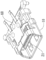
请同时参考图1A至图1C,图1A是显示根据本实用新型的一个实施例的D型HDMI连接器的分解立体图;图1B是显示根据本实用新型的一个实施例的D型HDMI连接器的仰视的分解立体图;图1C是显示根据本实用新型的一个实施例的D型HDMI连接器的组合立体图;图1D是显示根据本实用新型的一个实施例的D型HDMI连接器的另一视角的组合立体图。本实用新型的D型HDMI连接器100包含一遮蔽壳体10、一绝缘本体20、一屏蔽组件60、第一导电端子组30及第二导电端子组40,其中该遮蔽壳体10具有一容置空间101,该绝缘本体20设置于该容置空间101中且具有一舌板21,该舌板21的顶面设有多个间隔排列的第一端子槽210,而该舌板21的一外侧面设有多个间隔排列的第二端子槽211,该第一端子槽210及第二端子槽211用以将各导电端子间隔开,以防止相互接触而产生串扰。该屏蔽组件60置于该遮蔽壳体10的底面上,用以防止电磁干扰,而该多个第一导电端子组30对应置于该第一端子槽210中,且具有多个导电端子,而该多个第二导电端子组40则对应置于该第二端子槽211中。Please refer to Figure 1A to Figure 1C at the same time, Figure 1A is an exploded perspective view showing a D-type HDMI connector according to an embodiment of the present utility model; Figure 1B is an exploded perspective view showing a D-type HDMI connector according to an embodiment of the present utility model An exploded perspective view looking up; Figure 1C is a combined perspective view showing a D-type HDMI connector according to an embodiment of the present invention; Figure 1D is a perspective view showing another perspective of a D-type HDMI connector according to an embodiment of the present invention Combine stereograms. The D-type HDMI connector 100 of the present invention includes a shielding
进一步参考图2A至图2C,图2A是显示本实用新型的一个实施例的第一导电端子组的立体图;图2B是显示本实用新型的一个实施例的第二导电端子组的立体图;图2C是显示本实用新型的一个实施例的第一导电端子组与第二导电端子组组合的立体图。该第一导电端子组30的多个导电端子均具有一接触部31、多个弯折部32及焊接部33,该接触部31置于该绝缘壳体20的舌板21顶面的第一端子槽210中,且该第一导电端子组30的导电端子的接触部31置于该第一端子槽210中的端子排列顺序为一热插入侦测端子301、一第一高速讯号端子A(302)、一第一高速讯号端子B(303)、一第二高速讯号屏蔽端子304、一第三高速讯号端子A(305)、一第三高速讯号端子B(306)、一第四高速频率讯号屏蔽端子307、一消费性电子控制端子308、一串行频率端子309及一5伏特电源端子310,而该第二导电端子组40的多个导电端子也均具有一接触部41、多个弯折部42及焊接部43,该接触部31置于该绝缘壳体20的舌板21外侧面的第二端子槽211中,且该第二导电端子组40的导电端子的接触部31置于该第二端子槽211中的端子排列顺序为一通用信道端子401、一第一高速讯号屏蔽端子402、一第二高速讯号端子A(403)、一第二高速讯号端子B(404)、一第三高速讯号屏蔽端子405、一第四高速频率讯号端子A(406)、一第四高速频率讯号端子B(407)、一显示数据信道/消费性电子控制接地端子408及一串行数据端子409,藉由该第一导电端子组30的接触部31与该第二导电端子组40的接触部41分别置于该第一端子槽210及第二端子槽211中,使该第一导电端子组30与该第二导电端子组40形成端子上下排列,而多个弯折部32、42则由该接触部31、41分别朝该焊接部33、43多次弯折延伸,且藉由相互错置且多次弯折的该第一导电端子组30与第二导电端子组40,使该第一导电端子组30与该第二导电端子组40的焊接部33、43形成一水平直线排列,如图2C所示,且藉由该焊接部33、43呈一水平直线排列方式,有效地减少端子串音干扰问题。With further reference to Figures 2A to 2C, Figure 2A is a perspective view showing the first conductive terminal group of an embodiment of the present utility model; Figure 2B is a perspective view showing the second conductive terminal group of an embodiment of the present utility model; Figure 2C It is a perspective view showing the combination of the first conductive terminal group and the second conductive terminal group according to an embodiment of the present invention. The plurality of conductive terminals of the first
在本实施例中,该热插入侦测端子301和该第一高速讯号端子A(302)之间的间距与该串行频率端子309和该5伏特电源端子310之间的间距相同,而该第一高速讯号端子B(303)、该第二高速讯号屏蔽端子304、该第三高速讯号端子A(305)、该第三高速讯号端子B(306)、该第四高速频率讯号屏蔽端子307、该消费性电子控制端子308则以等间距依序排列,而使端子间形成规则性的对称,且该热插入侦测端子301和该第一高速讯号端子A(302)之间的间距与该串行频率端子309和该5伏特电源端子310之间的间距小于该第一高速讯号端子B(303)、该第二高速讯号屏蔽端子304、该第三高速讯号端子A(305)、该第三高速讯号端子B(306)、该第四高速频率讯号屏蔽端子307、该消费性电子控制端子308彼此间的间距。In this embodiment, the distance between the hot
而该通用通道端子401和该第一高速讯号屏蔽端子402之间的间距与该显示数据信道/消费性电子控制接地端子408和该串行数据端子409之间的间距相同,而该第二高速讯号端子A(403)、该第二高速讯号端子BThe distance between the
(404)、该第三高速讯号屏蔽端子405、该第四高速频率讯号端子A (406)、该第四高速频率讯号端子B(407)则以等间距依序排列,而使端子间形成规则性的对称,且该通用通道端子401和该第一高速讯号屏蔽端子402之间的间距与该显示数据信道/消费性电子控制接地端子408和该串行数据端子409之间的间距小于该第二高速讯号端子A(403)、该第二高速讯号端子B(404)、该第三高速讯号屏蔽端子405、该第四高速频率讯号端子A(406)、该第四高速频率讯号端子B(407)彼此间的间距。(404), the third high-speed
此外,在本实施例中,该第一高速讯号端子A(302)、第二高速讯号端子A(403)、第三高速讯号端子A(305)及第四高速频率讯号端子A(406)为一正讯号端子,而该第一高速讯号端子B(303)、第二高速讯号端子B(404)、第三高速讯号端子B(306)及第四高速频率讯号端子B(407)为一负讯号端子,且分别藉由该第一高速讯号屏蔽端子402、第二高速讯号屏蔽端子304、第三高速讯号屏蔽端子405及第四高速频率讯号屏蔽端子307降低端子间的干扰。In addition, in this embodiment, the first high-speed signal terminal A (302), the second high-speed signal terminal A (403), the third high-speed signal terminal A (305) and the fourth high-speed frequency signal terminal A (406) are A positive signal terminal, and the first high-speed signal terminal B (303), the second high-speed signal terminal B (404), the third high-speed signal terminal B (306) and the fourth high-speed frequency signal terminal B (407) are a negative Signal terminals, and the interference between the terminals is reduced by the first high-speed
此外,在本实施例中,该第一导电端子组30的接触部31端的导电端子所代表的脚位为奇数序列排列,即该热插入侦测端子301所代表的脚位为引脚1,而该第一高速讯号端子A(302)所代表的脚位依序为引脚3,该第一高速讯号端子B(303)所代表的脚位依序为引脚5,该第二高速讯号屏蔽端子304所代表的脚位为引脚7,而该第三高速讯号端子A(305)所代表的脚位依序为引脚9,该第三高速讯号端子B(306)所代表的脚位依序为引脚11,该第四高速频率讯号屏蔽端子307所代表的脚位为引脚13,而该消费性电子控制端子308所代表的脚位为引脚15,该串行频率端子309所代表的脚位为引脚17,而该5伏特电源端子310所代表的脚位为引脚19。In addition, in this embodiment, the pins represented by the conductive terminals at the
此外,在本实施例中,该第二导电端子组40的接触部31端的导电端子所代表的脚位为偶数序列排列,即该通用通道端子401所代表的脚位为引脚2,而该第一高速讯号屏蔽端子402所代表的脚位为引脚4,该第二高速讯号端子A(403)所代表的脚位依序为引脚6,该第二高速讯号端子B(404)所代表的脚位依序为引脚8,而该第三高速讯号屏蔽端子405所代表的脚位为引脚10,该第四高速频率讯号端子A(406)所代表的脚位依序为引脚12,该第四高速频率讯号端子B(407)所代表的脚位依序为引脚14,而该显示数据信道/消费性电子控制接地端子408所代表的脚位为引脚16,该串行资料端子409所代表的脚位为引脚18。In addition, in this embodiment, the pins represented by the conductive terminals at the
此外,本实用新型的D型HDMI连接器100,藉由相互错置且多次弯折该第一导电端子组30与第二导电端子组40,使该第一导电端子组30与第二导电端子组40的焊接部33、43端的导电端子呈一水平直线排列,且该水平直线排列的导电端子的引脚定义依序为该通用通道端子401、该热插入侦测端子301、该第一高速讯号端子A(302)、该第一高速讯号屏蔽端子402、该第一高速讯号端子B(303)、该第二高速讯号端子A(403)、该第二高速讯号屏蔽端子304、该第二高速讯号端子B(404)、该第三高速讯号端子A(305)、该第三高速讯号屏蔽端子(405)、该第三高速讯号端子B(306)、该第四高速频率讯号端子A(406)、该第四高速频率讯号屏蔽端子307、该第四高速频率讯号端子B(407)、该显示数据信道/消费性电子控制接地端子(308)、该消费性电子控制端子408、该串行频率端子309、该串行数据端子310及该5伏特电源端子409。In addition, the D-type HDMI connector 100 of the present invention makes the first
请参考图3A与图3B,图3A是显示本实用新型的一个实施例的D型HDMI连接器配合耦接的一电路板的分解示意图;图3B是显示本实用新型的一个实施例的D型HDMI连接器配合耦接的一电路板的组合示意图,其中本实用新型的D型HDMI连接器仅显示该第一导电端子组与第二导电端子组。本实用新型的D型HDMI连接器100用以耦接一电路板50上,该电路板50设有多个SMT接点51,该多个个SMT接点51呈水平直线排列,而该第一导电端子组30与第二导电端子组40的焊接部33根据引脚定义为该通用通道端子401、该热插入侦测端子301、该第一高速讯号端子A (302)、该第一高速讯号屏蔽端子402、该第一高速讯号端子B(303)、该第二高速讯号端子A(403)、该第二高速讯号屏蔽端子304、该第二高速讯号端子B(404)、该第三高速讯号端子A(305)、该第三高速讯号屏蔽端子(405)、该第三高速讯号端子B(306)、该第四高速频率讯号端子A(406)、该第四高速频率讯号屏蔽端子307、该第四高速频率讯号端子B(407)、该显示数据信道/消费性电子控制接地端子(308)、该消费性电子控制端子408、该串行频率端子309、该串行数据端子310及该5伏特电源端子409序列地间隔与该电路板50的多个SMT接点51耦接,如图3B所示,因此本实用新型的D型HDMI连接器100的水平直线排列的焊接部33、43的设计使该电路板50的电路布局(Layout)仅需设置一层,可有效地节省空间,相对地减少电路板的制作成本。Please refer to FIG. 3A and FIG. 3B. FIG. 3A is an exploded view showing a circuit board coupled with a D-type HDMI connector according to an embodiment of the present invention; FIG. 3B is a schematic diagram showing a D-type HDMI connector according to an embodiment of the present invention. A combined diagram of a circuit board coupled to the HDMI connector, wherein the D-type HDMI connector of the present invention only shows the first conductive terminal group and the second conductive terminal group. The D-type HDMI connector 100 of the present utility model is used for coupling on a
本实用新型的D型HDMI连接器,藉由该第一导电端子组30与第二导电端组40独特端子组排列结构,以减少电路板设计的成本与节省机壳的空间,且该第一导电端子组30与该第二导电端子组40的端子间形成规则性的对称,以使端子的模具结构简单,而容易制造,并藉由设置一屏蔽组件在该遮蔽壳体的底面上,而可防止电磁波的干扰。The D-type HDMI connector of the present utility model uses the unique terminal group arrangement structure of the first
在详细说明本实用新型的优选实施例之后,本领域的技术人员可清楚的了解,在不脱离权利要求范围与精神下可进行各种变化与改变,且本实用新型也不受限于说明书中所举实施例的实施方式。应注意,措词“包括”不排除其它元件或步骤,措词“一”或“一个”不排除多个。另外,权利要求的任何元件标号不应理解为限制本实用新型的范围。After describing the preferred embodiments of the present utility model in detail, those skilled in the art can clearly understand that various changes and changes can be made without departing from the scope and spirit of the claims, and the utility model is not limited to the specification. Implementation of the examples given. It should be noted that the word "comprising" does not exclude other elements or steps, and the word "a" or "an" does not exclude a plurality. Additionally, any element references in the claims should not be construed as limiting the scope of the present invention.
Claims (9)
Priority Applications (1)
| Application Number | Priority Date | Filing Date | Title |
|---|---|---|---|
| CN 201220301134 CN202662909U (en) | 2012-06-21 | 2012-06-21 | D type HDMI (High-Definition Multimedia Interface) connector |
Applications Claiming Priority (1)
| Application Number | Priority Date | Filing Date | Title |
|---|---|---|---|
| CN 201220301134 CN202662909U (en) | 2012-06-21 | 2012-06-21 | D type HDMI (High-Definition Multimedia Interface) connector |
Publications (1)
| Publication Number | Publication Date |
|---|---|
| CN202662909U true CN202662909U (en) | 2013-01-09 |
Family
ID=47457789
Family Applications (1)
| Application Number | Title | Priority Date | Filing Date |
|---|---|---|---|
| CN 201220301134 Expired - Fee Related CN202662909U (en) | 2012-06-21 | 2012-06-21 | D type HDMI (High-Definition Multimedia Interface) connector |
Country Status (1)
| Country | Link |
|---|---|
| CN (1) | CN202662909U (en) |
Cited By (13)
| Publication number | Priority date | Publication date | Assignee | Title |
|---|---|---|---|---|
| CN104158001A (en) * | 2013-05-31 | 2014-11-19 | 连展科技电子(昆山)有限公司 | Vertical electric connector |
| CN108075270A (en) * | 2016-11-16 | 2018-05-25 | 富士康(昆山)电脑接插件有限公司 | Electric connector |
| CN108448310A (en) * | 2018-04-24 | 2018-08-24 | 东莞联基电业有限公司 | HDMI connector and its conductive terminals |
| CN109149217A (en) * | 2017-06-15 | 2019-01-04 | 矽玛科技股份有限公司 | Signal connector using bending part to make terminal contact with grounding piece |
| TWI650910B (en) * | 2017-11-24 | 2019-02-11 | 維將科技股份有限公司 | Electrical connector |
| CN109378608A (en) * | 2014-04-09 | 2019-02-22 | 富士康(昆山)电脑接插件有限公司 | Socket connector |
| CN109462064A (en) * | 2018-11-28 | 2019-03-12 | 岱炜科技股份有限公司 | Structure of HDMI male connector |
| CN110048281A (en) * | 2018-01-15 | 2019-07-23 | 连展科技(深圳)有限公司 | Electrical connector |
| TWI682589B (en) * | 2018-10-19 | 2020-01-11 | 岱煒科技股份有限公司 | Structure of HDMI female connector (1) |
| CN110829075A (en) * | 2018-08-09 | 2020-02-21 | 岱炜科技股份有限公司 | Structure of HDMI male connector |
| CN110829076A (en) * | 2018-08-09 | 2020-02-21 | 岱炜科技股份有限公司 | Structure of HDMI female connector |
| CN111244657A (en) * | 2018-11-28 | 2020-06-05 | 岱炜科技股份有限公司 | Structure of HDMI socket connector |
| TWI908580B (en) * | 2024-11-28 | 2025-12-11 | 大陸商東莞立德精密工業有限公司 | A connector and accessories for an electronic equipment |
-
2012
- 2012-06-21 CN CN 201220301134 patent/CN202662909U/en not_active Expired - Fee Related
Cited By (15)
| Publication number | Priority date | Publication date | Assignee | Title |
|---|---|---|---|---|
| CN104158001A (en) * | 2013-05-31 | 2014-11-19 | 连展科技电子(昆山)有限公司 | Vertical electric connector |
| CN109378608A (en) * | 2014-04-09 | 2019-02-22 | 富士康(昆山)电脑接插件有限公司 | Socket connector |
| CN109378608B (en) * | 2014-04-09 | 2020-07-28 | 富士康(昆山)电脑接插件有限公司 | Socket connector |
| CN108075270A (en) * | 2016-11-16 | 2018-05-25 | 富士康(昆山)电脑接插件有限公司 | Electric connector |
| CN109149217A (en) * | 2017-06-15 | 2019-01-04 | 矽玛科技股份有限公司 | Signal connector using bending part to make terminal contact with grounding piece |
| CN109149217B (en) * | 2017-06-15 | 2020-04-07 | 矽玛科技股份有限公司 | Signal connector using bending part to make terminal contact with grounding piece |
| TWI650910B (en) * | 2017-11-24 | 2019-02-11 | 維將科技股份有限公司 | Electrical connector |
| CN110048281A (en) * | 2018-01-15 | 2019-07-23 | 连展科技(深圳)有限公司 | Electrical connector |
| CN108448310A (en) * | 2018-04-24 | 2018-08-24 | 东莞联基电业有限公司 | HDMI connector and its conductive terminals |
| CN110829075A (en) * | 2018-08-09 | 2020-02-21 | 岱炜科技股份有限公司 | Structure of HDMI male connector |
| CN110829076A (en) * | 2018-08-09 | 2020-02-21 | 岱炜科技股份有限公司 | Structure of HDMI female connector |
| TWI682589B (en) * | 2018-10-19 | 2020-01-11 | 岱煒科技股份有限公司 | Structure of HDMI female connector (1) |
| CN111244657A (en) * | 2018-11-28 | 2020-06-05 | 岱炜科技股份有限公司 | Structure of HDMI socket connector |
| CN109462064A (en) * | 2018-11-28 | 2019-03-12 | 岱炜科技股份有限公司 | Structure of HDMI male connector |
| TWI908580B (en) * | 2024-11-28 | 2025-12-11 | 大陸商東莞立德精密工業有限公司 | A connector and accessories for an electronic equipment |
Similar Documents
| Publication | Publication Date | Title |
|---|---|---|
| CN202662909U (en) | D type HDMI (High-Definition Multimedia Interface) connector | |
| US9136649B2 (en) | HDMI type-D connector | |
| CN202217817U (en) | Connector for Mini DisplayPort | |
| CN104795700B (en) | Audio-video signal transmission connector | |
| US8083546B2 (en) | Electric connector and electric assembly | |
| TWI339467B (en) | Electrical connector and cable | |
| CN102292881A (en) | Receptacle, printed wiring board, and electronic device | |
| TWM496274U (en) | Connector improvement | |
| CN113810070B (en) | Signal transmission device capable of transmitting multiple sets of data streams | |
| US7963809B2 (en) | Microdvi connector | |
| CN102117978A (en) | Electric connector | |
| CN201160154Y (en) | stackable connector | |
| CN103117463A (en) | Display port connector and circuit board in coupling connection with the same | |
| CN102239606A (en) | Receptacle, printed circuit board, and electronic device | |
| KR101092155B1 (en) | HMD Connector | |
| US8007322B2 (en) | Connector component and connector device | |
| CN201639086U (en) | Electric connector | |
| US10404021B2 (en) | Reliable connector receptacles having high signal quality | |
| CN108448310A (en) | HDMI connector and its conductive terminals | |
| CN111082267A (en) | Multipoint grounded electric connector | |
| CN204067706U (en) | Improved structure of the connector | |
| CN201336463Y (en) | Connecting device with built-in digital television tuner | |
| US8690458B2 (en) | Optical connector | |
| CN110011091B (en) | electrical connector | |
| TWI478445B (en) | Display port connector and a circuit board coupled thereto |
Legal Events
| Date | Code | Title | Description |
|---|---|---|---|
| C14 | Grant of patent or utility model | ||
| GR01 | Patent grant | ||
| CF01 | Termination of patent right due to non-payment of annual fee |
Granted publication date: 20130109 Termination date: 20200621 |
|
| CF01 | Termination of patent right due to non-payment of annual fee |