CN1758322A - Display element drive unit, display device including the same, and display element drive method - Google Patents
Display element drive unit, display device including the same, and display element drive method Download PDFInfo
- Publication number
- CN1758322A CN1758322A CNA2005101165568A CN200510116556A CN1758322A CN 1758322 A CN1758322 A CN 1758322A CN A2005101165568 A CNA2005101165568 A CN A2005101165568A CN 200510116556 A CN200510116556 A CN 200510116556A CN 1758322 A CN1758322 A CN 1758322A
- Authority
- CN
- China
- Prior art keywords
- display
- mentioned
- circuit
- data
- display element
- Prior art date
- Legal status (The legal status is an assumption and is not a legal conclusion. Google has not performed a legal analysis and makes no representation as to the accuracy of the status listed.)
- Granted
Links
Images


Classifications
-
- G—PHYSICS
- G09—EDUCATION; CRYPTOGRAPHY; DISPLAY; ADVERTISING; SEALS
- G09G—ARRANGEMENTS OR CIRCUITS FOR CONTROL OF INDICATING DEVICES USING STATIC MEANS TO PRESENT VARIABLE INFORMATION
- G09G3/00—Control arrangements or circuits, of interest only in connection with visual indicators other than cathode-ray tubes
- G09G3/20—Control arrangements or circuits, of interest only in connection with visual indicators other than cathode-ray tubes for presentation of an assembly of a number of characters, e.g. a page, by composing the assembly by combination of individual elements arranged in a matrix no fixed position being assigned to or needed to be assigned to the individual characters or partial characters
- G09G3/34—Control arrangements or circuits, of interest only in connection with visual indicators other than cathode-ray tubes for presentation of an assembly of a number of characters, e.g. a page, by composing the assembly by combination of individual elements arranged in a matrix no fixed position being assigned to or needed to be assigned to the individual characters or partial characters by control of light from an independent source
- G09G3/36—Control arrangements or circuits, of interest only in connection with visual indicators other than cathode-ray tubes for presentation of an assembly of a number of characters, e.g. a page, by composing the assembly by combination of individual elements arranged in a matrix no fixed position being assigned to or needed to be assigned to the individual characters or partial characters by control of light from an independent source using liquid crystals
- G09G3/3611—Control of matrices with row and column drivers
- G09G3/3685—Details of drivers for data electrodes
- G09G3/3688—Details of drivers for data electrodes suitable for active matrices only
-
- G—PHYSICS
- G02—OPTICS
- G02F—OPTICAL DEVICES OR ARRANGEMENTS FOR THE CONTROL OF LIGHT BY MODIFICATION OF THE OPTICAL PROPERTIES OF THE MEDIA OF THE ELEMENTS INVOLVED THEREIN; NON-LINEAR OPTICS; FREQUENCY-CHANGING OF LIGHT; OPTICAL LOGIC ELEMENTS; OPTICAL ANALOGUE/DIGITAL CONVERTERS
- G02F1/00—Devices or arrangements for the control of the intensity, colour, phase, polarisation or direction of light arriving from an independent light source, e.g. switching, gating or modulating; Non-linear optics
- G02F1/01—Devices or arrangements for the control of the intensity, colour, phase, polarisation or direction of light arriving from an independent light source, e.g. switching, gating or modulating; Non-linear optics for the control of the intensity, phase, polarisation or colour
- G02F1/13—Devices or arrangements for the control of the intensity, colour, phase, polarisation or direction of light arriving from an independent light source, e.g. switching, gating or modulating; Non-linear optics for the control of the intensity, phase, polarisation or colour based on liquid crystals, e.g. single liquid crystal display cells
- G02F1/133—Constructional arrangements; Operation of liquid crystal cells; Circuit arrangements
-
- G—PHYSICS
- G09—EDUCATION; CRYPTOGRAPHY; DISPLAY; ADVERTISING; SEALS
- G09G—ARRANGEMENTS OR CIRCUITS FOR CONTROL OF INDICATING DEVICES USING STATIC MEANS TO PRESENT VARIABLE INFORMATION
- G09G3/00—Control arrangements or circuits, of interest only in connection with visual indicators other than cathode-ray tubes
- G09G3/20—Control arrangements or circuits, of interest only in connection with visual indicators other than cathode-ray tubes for presentation of an assembly of a number of characters, e.g. a page, by composing the assembly by combination of individual elements arranged in a matrix no fixed position being assigned to or needed to be assigned to the individual characters or partial characters
- G09G3/34—Control arrangements or circuits, of interest only in connection with visual indicators other than cathode-ray tubes for presentation of an assembly of a number of characters, e.g. a page, by composing the assembly by combination of individual elements arranged in a matrix no fixed position being assigned to or needed to be assigned to the individual characters or partial characters by control of light from an independent source
- G09G3/36—Control arrangements or circuits, of interest only in connection with visual indicators other than cathode-ray tubes for presentation of an assembly of a number of characters, e.g. a page, by composing the assembly by combination of individual elements arranged in a matrix no fixed position being assigned to or needed to be assigned to the individual characters or partial characters by control of light from an independent source using liquid crystals
- G09G3/3611—Control of matrices with row and column drivers
- G09G3/3648—Control of matrices with row and column drivers using an active matrix
-
- G—PHYSICS
- G09—EDUCATION; CRYPTOGRAPHY; DISPLAY; ADVERTISING; SEALS
- G09G—ARRANGEMENTS OR CIRCUITS FOR CONTROL OF INDICATING DEVICES USING STATIC MEANS TO PRESENT VARIABLE INFORMATION
- G09G2310/00—Command of the display device
- G09G2310/02—Addressing, scanning or driving the display screen or processing steps related thereto
- G09G2310/0243—Details of the generation of driving signals
- G09G2310/0245—Clearing or presetting the whole screen independently of waveforms, e.g. on power-on
-
- G—PHYSICS
- G09—EDUCATION; CRYPTOGRAPHY; DISPLAY; ADVERTISING; SEALS
- G09G—ARRANGEMENTS OR CIRCUITS FOR CONTROL OF INDICATING DEVICES USING STATIC MEANS TO PRESENT VARIABLE INFORMATION
- G09G2310/00—Command of the display device
- G09G2310/02—Addressing, scanning or driving the display screen or processing steps related thereto
- G09G2310/0264—Details of driving circuits
- G09G2310/027—Details of drivers for data electrodes, the drivers handling digital grey scale data, e.g. use of D/A converters
-
- G—PHYSICS
- G09—EDUCATION; CRYPTOGRAPHY; DISPLAY; ADVERTISING; SEALS
- G09G—ARRANGEMENTS OR CIRCUITS FOR CONTROL OF INDICATING DEVICES USING STATIC MEANS TO PRESENT VARIABLE INFORMATION
- G09G2320/00—Control of display operating conditions
- G09G2320/02—Improving the quality of display appearance
- G09G2320/0271—Adjustment of the gradation levels within the range of the gradation scale, e.g. by redistribution or clipping
- G09G2320/0276—Adjustment of the gradation levels within the range of the gradation scale, e.g. by redistribution or clipping for the purpose of adaptation to the characteristics of a display device, i.e. gamma correction
Landscapes
- Engineering & Computer Science (AREA)
- Physics & Mathematics (AREA)
- General Physics & Mathematics (AREA)
- Crystallography & Structural Chemistry (AREA)
- Chemical & Material Sciences (AREA)
- Theoretical Computer Science (AREA)
- Computer Hardware Design (AREA)
- Nonlinear Science (AREA)
- Mathematical Physics (AREA)
- Optics & Photonics (AREA)
- Control Of Indicators Other Than Cathode Ray Tubes (AREA)
- Liquid Crystal Display Device Control (AREA)
- Liquid Crystal (AREA)
Abstract
显示元件驱动装置设置有电源接通时间显示部,该电源接通时间显示部为了可以从显示面板的电源接通时刻起直到输出基于被输入的显示数据信号的灰度显示电平电压的一定期间内,将和基于该被输入的显示数据信号的灰度显示电平电压不同的灰度显示电平电压输出到多个显示元件,而预先另外设定灰度显示数字数据。由此,将提供对于面板电源接通时的一定期间内产生的瞬间显示图像的紊乱,能够在将电路尺寸的增大控制在最小限度的条件下减轻该问题的显示元件驱动装置,具有该显示元件驱动装置的显示装置以及显示元件驱动方法。

The display element driving device is provided with a power-on time display unit for a certain period from when the power of the display panel is turned on until outputting a gradation display level voltage based on an input display data signal. Inside, a grayscale display level voltage different from the grayscale display level voltage based on the input display data signal is output to a plurality of display elements, and grayscale display digital data is separately set in advance. Thus, there will be provided a display element driving device capable of alleviating the disturbance of the displayed image instantaneously during a certain period of time when the panel power is turned on, while minimizing the increase in the circuit size. A display device of an element driving device and a display element driving method.
Description
发明领域field of invention
本发明涉及驱动多个液晶显示元件等等的显示元件的显示元件驱动装置,和具有该显示元件驱动装置的显示装置以及显示元件驱动方法。作为显示装置,例如可以在有源矩阵型液晶显示装置中使用,并且在电泳型显示器、螺旋球型显示器(twist ball display)、利用微细的棱柱薄膜的反射型显示器、利用数字反射镜装置等光学调制元件的显示器等等中使用外,还可以作为发光元件,在使用有机EL发光元件、无机EL发光元件、LED(发光二极管)等发光亮度可变的元件的显示器、场致发光显示器(FED)、等离子体显示器等等中使用。The present invention relates to a display element driving device for driving display elements such as a plurality of liquid crystal display elements, a display device including the display element driving device, and a display element driving method. As a display device, for example, it can be used in an active matrix liquid crystal display device, and in an electrophoretic display, a twist ball display (twist ball display), a reflective display using a fine prism film, and an optical device using a digital mirror device. In addition to being used in displays such as modulation elements, it can also be used as a light-emitting element in displays using elements with variable luminance such as organic EL light-emitting elements, inorganic EL light-emitting elements, LEDs (light-emitting diodes), and electroluminescence displays (FED). , Plasma Display, etc. used.
背景技术Background technique
在液晶显示装置的各种显示方式中,包含有一种作为进行高精密显示的方式的,在开关元件中采用TFT(Thin Film Transistor:薄膜晶体管)的有源矩阵方式。Among the various display methods of liquid crystal display devices, there is an active matrix method using TFT (Thin Film Transistor: Thin Film Transistor) as a switching element as a method for high-precision display.
如图13所示,采用着上述有源矩阵方式的液晶显示装置110的结构大致可以分为液晶显示部110a,和作为驱动该液晶显示部110a的液晶驱动装置的液晶驱动电路110b。As shown in FIG. 13, the structure of the liquid
上述液晶显示部110a具有呈TFT方式的液晶面板101。另一方面,在上述液晶驱动电路110b上,搭载有由IC(Integrated Circuit:半导体集成电路)构成的源极驱动器103、栅极驱动器104、控制器105和液晶驱动电源106。The liquid crystal display unit 110a has a
在上述结构的液晶显示装置110中,从外部输入的显示数据通过上述控制器105作为数字信号即显示数据D被输入到源极驱动器103中。源极驱动器103对输入的显示数据D进行时间分割,并锁存在第1源极驱动器~第n源极驱动器中,之后,与从控制器105输入的上述水平同步信号同步并进行D/A(数/模)变换。然后,通过未图示的源极信号线,将对按时间分割的显示数据D进行D/A变换的灰度显示用的模拟电压(下面也称为“灰度显示电压”),输出到液晶面板101内对应的液晶显示元件中。In the liquid
另一方面,如图14所示,在上述液晶面板101上设置有象素电极111、象素电容112、对将电压施加到象素电极111上进行开·关控制的TFT(Thin FilmTransistor:薄膜晶体管)113、源极信号线114、栅极信号线115以及对置电极102。这里,由象素电极111、象素电容112和TFT113构成1个象素的液晶显示元件A。On the other hand, as shown in FIG. 14, the above-mentioned
将对应于显示对象象素的亮度的上述灰度显示电压,从图13所示的源极驱动器103施加到上述源极信号线114上。另一方面,将依次接通按列方向排列的TFT113的扫描信号从栅极驱动器104施加到栅极信号线115上。然后,通过处于导通状态的TFT113将源极信号线114的灰度显示电压,施加到连接到该TFT113的漏极上的象素电极111上,并积累在和上述对置电极102之间的象素电容112上。这样,液晶的透光率将对应于上述灰度显示电压而发生变化,进行象素显示。The gradation display voltage corresponding to the luminance of the pixel to be displayed is applied to the source signal line 114 from the
下面,基于图15对构成源极驱动器103的第n源极驱动器进行说明。Next, the nth source driver constituting the
如该图所示,在第n源极驱动器130,作为输入的数字信号的显示数据D具有分别为R(赤)·G(绿)·B(蓝)的显示数据(DR·DG·DB)。该显示数据D在被暂时锁存在输入锁存电路131中后,配合根据来自上述控制器105的启动脉冲信号SP和时钟信号CK实施移位的移位寄存电路132的动作,通过时间分割方式存储在采样存储电路133中。之后,基于来自控制器105的未图示的水平同步信号一起传送到保持存储电路134中。而且,S表示的是串级输出(cascade output)。As shown in the figure, in the nth source driver 130, the display data D as an input digital signal has display data (DR·DG·DB) of R (red), G (green) and B (blue), respectively. . After the display data D is temporarily latched in the input latch circuit 131, it cooperates with the operation of the shift register circuit 132 for shifting according to the start pulse signal SP and the clock signal CK from the above-mentioned
基于从外部基准电压产生电路(相当于图13中的液晶驱动电源106)供给的电压VR,灰度显示基准电压产生电路139可以产生出各种电平的基准电压。保持存储电路134的数据通过电平移位电路135输出到D/A变换电路136中,并基于各种电平的基准电压被变换成模拟电压。然后,由输出电路137从液晶驱动电压输出端子138(如图15示出的R1、G1、B1~Rn、Gn、Bn端子),作为上述灰度显示电压输出到各液晶显示元件A的源极信号线114上。换言之,上述基准电压的电平数为上述可以显示的灰度数。Based on the voltage VR supplied from the external reference voltage generating circuit (corresponding to the liquid crystal
如图16所示,产生上述这样的多个基准电压并生成中间电压用的灰度显示基准电压产生电路139,可以产生出通常为64种的基准电压。As shown in FIG. 16, the gradation display reference voltage generation circuit 139 for generating a plurality of reference voltages as described above to generate an intermediate voltage can generate 64 kinds of reference voltages in general.
该灰度显示基准电压产生电路139可以由下述各部分构成,即由V0·V8·V16·V24·V32·V40·V48·V56和V64表示的9个中间色调电压输入端子,具有用于γ校正的电阻比的电阻元件R0~R7,以及在各电阻元件R0~R7的两端之间每8个串联连接总共为64个的未图示的电阻。采用这种方式,可以将具有被称为γ校正的电阻比内置于源极驱动器103中,使得在用于变换到上述灰度显示电压的液晶驱动输出电压具有折线特性(broken linecharacteristic)。因此,通过利用上述电阻比的比率校正液晶材料的光学特性,将能够进行符合液晶材料的光学特性的自然的灰度显示。而且,在图17中示出了在现有的灰度显示基准电压产生电路139中实施γ校正的液晶驱动输出电压的特性实例。The gradation display reference voltage generation circuit 139 can be composed of the following parts, that is, nine halftone voltage input terminals represented by V0 V8 V16 V24 V32 V40 V48 V56 and V64, with Resistive elements R0 to R7 having a corrected resistance ratio, and a total of 64 unshown resistors are connected in series every 8 between both ends of the respective resistive elements R0 to R7 . In this way, a resistance ratio called gamma correction can be built into the
如图18所示,栅极驱动器104由控制·逻辑电路161、双向移位寄存器162、电平移位器163以及输出电路164等构成。栅极驱动器104具有用于引入启动脉冲信号SP和时钟信号CK、电源电压VCC、接地电压GND、电压VDD的端子、以及多个输出端子OS1~OSn。As shown in FIG. 18 , the
控制·逻辑电路161生成双向移位寄存器162的动作需要的信号,并提供给该双向移位寄存器162。双向移位寄存器162被提供了时钟信号CK和启动脉冲信号SP时,按照依次使该启动脉冲信号SP和时钟信号CK同步的方式进行移位动作。双向移位寄存器162生成选择脉冲,并输出到电平移位器163中,该选择脉冲用于选择利用从源极驱动器103施加到源极信号线114…上的电压驱动的液晶面板101的象素电极。电平移位器163将选择脉冲的电平变换为液晶面板101具备的TFT元件113的ON/OFF(选择/非选择)所需要的电平,并输出到输出电路164中。The control/
输出电路164基于从电平移位器163输入的信号,将上述TFT元件113的ON/OFF所需电平的电压通过对应的输出端子OS1~OSn,施加到栅极信号线115上。换言之,可以如图19所示,使输出电路164在被提供有作为电压VCC的输入信号时,将作为电压VDD的输出信号依次提供给输出端子OS1~OSn,另一方面,在没有被提供输入信号时(电压GND),将作为电压VSS的输出信号提供给输出端子OS1~OSn。The
然而,在具有这样构成形式的现有显示元件驱动装置中,是通过图13所示的控制器105提供显示控制输入信号的。因此,在面板动作开始电源接通之后的控制器动作前的状态下,因为显示数据信号和输入控制信号尚没有被提供给如图13所示的源极驱动器103和栅极驱动器104,所以提供至液晶面板101中各个驱动器输出端子的电位状态仍为不定状态。However, in the conventional display element driving apparatus having such a constitution, the display control input signal is supplied through the
因此,由于电源接通时面板侧的栅极元件的电位状态,该不定的电位会被加到源极电位上,根据面板的特性,存在有在扫描线的一部分、或者面板整体上瞬间不能进行预期显示的可能性。Therefore, due to the potential state of the gate element on the panel side when the power is turned on, this indeterminate potential is added to the source potential, and depending on the characteristics of the panel, some scan lines or the entire panel may be momentarily disabled. Possibility of expected showing.
为了能够避免这一现像出现,在例如日本公开专利公报《特开2004-4244号公报(公开日2004年1月8日)》中,采用的方法是在灰度选择单元(DA变换器)和液晶面板电极之间配备输出切换单元,并利用该切换向面板电极或者外部对置电极CS输出施加另行设定的一定电压。In order to avoid this phenomenon, for example, in the Japanese Laid-Open Patent Publication "JP-A-2004-4244 (Disclosure Date January 8, 2004)", the method adopted is to use the grayscale selection unit (DA converter) An output switching unit is provided between the liquid crystal panel electrode and the output of the panel electrode or the external counter electrode CS is used to apply a certain voltage that is set separately.
然而在上述现有的显示元件驱动装置中,如果采用日本特开2004-4244号公报公开的技术,为了防止灰度显示电压的电压下降,需要减小切换单元(诸如模拟开关等)的电阻,所以存在有下述问题,即对由DA变换器实施变换后的模拟电位实施切换的单元(诸如模拟CMOS等)的电路面积会变得非常大。However, in the above-mentioned conventional display element driving device, if the technique disclosed in Japanese Patent Laid-Open No. 2004-4244 is adopted, in order to prevent the voltage drop of the grayscale display voltage, it is necessary to reduce the resistance of the switching unit (such as an analog switch, etc.), Therefore, there is a problem that the circuit area of a unit (such as an analog CMOS) for switching the analog potential converted by the DA converter becomes very large.
换言之,在由图20所示的模拟开关构成切换电位的单元时,在显示元件驱动装置中通常由DA变换器201将显示数据变换到模拟灰度选择电位,通过利用例如运算放大电路的输出电路202使其进一步低阻抗化,作为液晶象素源极电位A进行模拟电位输出。In other words, when the analog switch shown in FIG. 20 constitutes a unit for switching potentials, in the display element driving device, the display data is usually converted into an analog grayscale selection potential by a
此时,对于采用构成为日本特开2004-4244号公报公开的形式的情况下,为了能够在电源接通之后的一定期间内对液晶象素施加一定的电压,或者向外部对置电极CS实施输出,需要象同一图形中所示的那样,设置将象素电位提供给对置电极的切换开关210。At this time, in the case of adopting the configuration disclosed in Japanese Patent Application Laid-Open No. 2004-4244, in order to apply a certain voltage to the liquid crystal pixel within a certain period of time after the power is turned on, or to apply a voltage to the external counter electrode CS For output, it is necessary to provide a
然而,对于在对被模拟变换的模拟灰度选择电位进行低阻抗处理之后设置切换开关210的情况下,模拟开关部211的电阻阻抗的影响会施加到低阻抗化的模拟电位即液晶象素源极电位A上直到到达象素。因为该电阻阻抗成分,例如模拟信号的时间常数、过渡特性、或者随着转换速率的增大而使到达时间延迟引起的电位下降等对象素电位切换的速度产生的影响,需要设计为符合面板特性并尽量减小模拟开关部211的导通电阻。因此,在用要求达到某种程度的耐压的模拟电路构成该开关的情况下,伴随着导通阻抗减小的设计,不得不将晶体管尺寸设计得比较大,因此相对而言电路尺寸变大了。However, when the
而且,在由切换开关210反向输出公共电位,提供给公共电极的情况下,模拟开关部211需要采用具有瞬态响应(transient response)能力的公共电位的缓冲器结构、低阻抗结构。因此,需要随着公共电极的驱动能力减小电路阻抗,相对而言电路会变大。In addition, when the common potential is reversely output by the
发明内容Contents of the invention
本发明的目的是提供一种对于面板电源接通时的一定期间内产生的瞬间显示图像的紊乱,能够在将电路尺寸的增大控制在最小限度的条件下减轻该不正常显示问题的显示元件驱动装置,具有该显示元件驱动装置的显示装置以及显示元件驱动方法。The object of the present invention is to provide a display element capable of alleviating the problem of abnormal display while minimizing the increase in the circuit size when the display image is disturbed for a certain period of time when the power supply of the panel is turned on. A driving device, a display device having the display element driving device, and a display element driving method.
为了达到上述目的,本发明提供的显示元件驱动装置是一种对包含多个显示元件的显示面板实施显示驱动的显示元件驱动装置,设置有电源接通时间显示单元,该电源接通时间显示单元为了能够从上述显示面板的电源接通时刻起直到输出基于被输入的显示数据信号的灰度显示电平电压的一定期间内,将和基于该被输入的显示数据信号的灰度显示电平电压不同的灰度显示电平电压输出到上述多个显示元件,而预先另外设定灰度显示数字数据。In order to achieve the above object, the display element driving device provided by the present invention is a display element driving device for performing display driving on a display panel including a plurality of display elements, and is provided with a power-on time display unit, and the power-on time display unit In order to combine the grayscale display level voltage based on the input display data signal with the grayscale display level voltage based on the input display data signal for a certain period from when the display panel is powered on until the output of the grayscale display level voltage based on the input display data signal Different grayscale display level voltages are output to the above-mentioned plurality of display elements, and grayscale display digital data is additionally set in advance.
而且,为了达到上述目的,本发明提供的显示元件驱动方法是对包含多个显示元件的显示面板实施显示驱动的显示元件驱动方法,在从上述显示面板的电源接通时刻直到输出基于被输入的显示数据信号的灰度显示电平电压的一定期间内,预先另外设定灰度显示数字数据,并将该灰度显示数字数据变换为模拟的灰度显示电平电压,输出到上述多个显示元件。Moreover, in order to achieve the above object, the display element driving method provided by the present invention is a display element driving method for performing display driving on a display panel including a plurality of display elements. During a certain period of the gray-scale display level voltage of the display data signal, the gray-scale display digital data is separately set in advance, and the gray-scale display digital data is converted into an analog gray-scale display level voltage, and output to the above-mentioned multiple displays element.
换言之,从显示面板的电源接通时直到输出基于被输入的显示数据信号的灰度显示电平电压的一定期间内,由于显示面板上的显示元件的栅极电位的状态,会将不定的电位加到源极电位上,所以根据显示面板的特性,存在有在扫描线的一部分或者显示面板整体上瞬间没有进行预期显示的可能性。In other words, during a certain period from when the power supply of the display panel is turned on until the output of the grayscale display level voltage based on the input display data signal, the variable potential is changed due to the state of the gate potential of the display element on the display panel. Since it is added to the source potential, depending on the characteristics of the display panel, there is a possibility that a part of the scanning lines or the entire display panel may not perform the desired display for a moment.
为了防止这一问题出现,可以考虑在显示元件驱动装置和显示面板之间设置模拟开关部,从而在面板电源接通时的一定期间内能够另行施加一定电压。然而如果采用该方法,为了能够防止灰度显示电压的电压下降,需要减小模拟开关部的电阻,所以模拟开关装置的电路面积会变得非常大。In order to prevent this problem, it is conceivable to provide an analog switch unit between the display element driving device and the display panel so that a certain voltage can be separately applied for a certain period when the panel power is turned on. However, according to this method, in order to prevent the voltage drop of the gray scale display voltage, it is necessary to reduce the resistance of the analog switch section, so the circuit area of the analog switch device becomes very large.
在本发明中,电源接通时间显示部为了可以从显示面板的电源接通时直到输出基于被输入的显示数据信号的灰度显示电平电压的一定期间内,将和基于该被输入的显示数据信号的灰度显示电平电压不同的灰度显示电平电压输出到上述多个显示元件,而预先另外设定灰度显示数字数据。In the present invention, the power-on time display unit displays the gray-scale display level voltage based on the input display data signal for a certain period from when the power of the display panel is turned on until outputting the grayscale display level voltage based on the input display data signal. The grayscale display level voltages different from the grayscale display level voltages of the data signals are output to the plurality of display elements, and the grayscale display digital data is separately set in advance.
因此,在本发明中,可以基本通过数字部,在电源接通时的显示不定期间固定在预先另外设定的灰度显示数字数据。由此,因为可以按数字形式设计电路结构,所以可以设计得远小于利用模拟回路的开关部。Therefore, in the present invention, it is basically possible to display digital data at a previously set gradation during an indeterminate display period when the power is turned on by the digital unit. As a result, since the circuit configuration can be designed in a digital format, it can be designed much smaller than the switching section using an analog circuit.
另外,DA变换电路可以按照现有技术中的方式加以利用,所以不会影响模拟输出的驱动能力。In addition, the DA conversion circuit can be used in the prior art, so the driving capability of the analog output will not be affected.
其结果是,本发明能够提供出一种对于面板电源接通时的一定期间内产生的瞬间显示图像的紊乱,能够在将电路尺寸的增大控制在最小限度的条件下减轻其不正常显示问题的显示元件驱动装置以及显示元件驱动方法。As a result, the present invention can provide a method for temporarily displaying image disturbances that occur within a certain period of time when the power supply of the panel is turned on, and can reduce the problem of abnormal display while controlling the increase in circuit size to a minimum. A display element driving device and a display element driving method.
而且,本发明的显示元件驱动装置还可以在上述记载的显示元件驱动装置中,进一步具有传送部,传送基于时钟信号的启动脉冲信号;锁存部,使输入的显示数据信号与时钟信号同步引入,并作为同步数据输出;采样部,基于传送的启动脉冲信号对上述同步数据进行采样并输出;电平移位部,使采样的上述同步数据升压;数-模变换部,对从上述采样部输出的数字数据进行数-模变换;输出部,将由上述数-模变换部得到的灰度显示用模拟电压输出到上述多个显示元件中,同时,上述电源接通时间显示部具有:电源接通时间判断部,判断上述显示面板的电源是否已接通;切换部,切换预先另外设定的灰度显示数字数据和基于输入的显示数据信号的灰度显示数字数据;以及切换控制部,基于由上述电源接通时间判断部进行的电源是否接通的判断,控制上述切换部中的预先另外设定的灰度显示数字数据和基于输入的显示数据信号的灰度显示数字数据之间的切换。Moreover, the display element driving device of the present invention may further include a transmission part for transmitting a start pulse signal based on a clock signal in the display element driving device described above; a latch part for synchronously introducing the input display data signal and the clock signal. , and output as synchronous data; the sampling unit samples and outputs the above-mentioned synchronous data based on the transmitted start pulse signal; the level shift unit boosts the above-mentioned synchronous data sampled; the digital-to-analog conversion unit performs The output digital data is subjected to digital-to-analog conversion; the output unit outputs the analog voltage for gray scale display obtained by the above-mentioned digital-to-analog conversion unit to the above-mentioned multiple display elements, and at the same time, the above-mentioned power-on time display unit has: The on-time judging part judges whether the power supply of the above-mentioned display panel has been turned on; the switching part switches the grayscale display digital data set in advance and the grayscale display digital data based on the input display data signal; and the switching control part based on The determination of whether or not the power is turned on by the power-on time judging section controls the switching between the previously set grayscale display digital data and the grayscale display digital data based on the input display data signal in the switching section. .
如果采用上述发明,电源接通时间显示部被配置在电平移位部的前面。由此,可以基本上通过数字部,在电源接通时的显示不定期间固定在预先另外设定的灰度显示数字数据上。而且,因为电平移位部的前级是由3~5V电源驱动的低电压驱动部,所以通过在该低电压驱动部中设置电源接通时间显示部的方式,能够将电路的增大控制在最小限度。According to the above invention, the power-on time display section is arranged in front of the level shift section. Thereby, basically, the digital part can be fixed to the previously set gradation display digital data during the display indefinite period when the power is turned on. Moreover, since the front stage of the level shifting part is a low-voltage driving part driven by a 3-5V power supply, by providing a power-on time display part in the low-voltage driving part, the increase of the circuit can be controlled at minimum.
而且,因为传送基于时钟信号的启动脉冲信号的传送部、锁存部、采样部、电平移位部、数-模变换部以及输出部均可以采用和现有的显示元件驱动装置中相同的结构,所以还能够在维持属于现有的面板周边部件的设置状态下,解决电源接通时的瞬间显示不正常的问题。Moreover, because the transmitting part, latching part, sampling part, level shifting part, digital-to-analog converting part and outputting part which transmit the start pulse signal based on the clock signal can all adopt the same structure as that in the existing display element driving device , Therefore, it is also possible to solve the problem of abnormal display at the moment when the power is turned on while maintaining the installation state of the existing panel peripheral components.
而且,电源接通时间显示部可以具有判断显示面板的电源是否已接通的电源接通时间判断部,切换预先另外设定的灰度显示数字数据和基于输入的显示数据信号的灰度显示数字数据的切换部,和基于由上述电源接通时间判断部判断出的电源接通判断结果,控制上述切换部中的预先另外设定的灰度显示数字数据和基于输入的显示数据信号的灰度显示数字数据之间切换的切换控制部。Furthermore, the power-on time display unit may have a power-on time judging unit for judging whether or not the power of the display panel has been turned on, and switches between previously set gray scale display digital data and gray scale display digital data based on an input display data signal. A data switching section, and based on the power-on judgment result judged by the power-on time judging section, controls the previously set grayscale display digital data in the switching section and the grayscale based on the input display data signal. Display switching control section for switching between digital data.
因此,本发明还能够提供电源接通时间显示部的具体结构。Therefore, the present invention can also provide a specific structure of the power-on time display unit.
而且,因为进行数-模变换的数-模变换部一般来说,能够利用灰度显示基准电压产生电路和调整放大器的结构产生出所期望的中间电压,所以电源接通时的显示电位可以依照已有的灰度变换方式实施输出。因此,能够实现电路尺寸的缩小和端子数的削减,且能够抑制制造成本。In addition, since the digital-analog conversion unit that performs digital-analog conversion can generally generate a desired intermediate voltage by using the structure of the gray scale display reference voltage generation circuit and the adjustment amplifier, the display potential when the power is turned on can be in accordance with the established Some grayscale conversion methods implement output. Therefore, reduction in circuit size and reduction in the number of terminals can be achieved, and manufacturing costs can be suppressed.
而且,为了解决上述问题,本发明提供的显示装置可以具有上述记载的显示元件驱动装置。Furthermore, in order to solve the above problems, the display device provided by the present invention may include the display element driving device described above.
如果采用上述发明,将能够提供出一种具有对于面板电源接通时的一定期间内产生的瞬间显示图像的紊乱,能够在将电路尺寸的增大控制在最小限度的条件下减轻该不正常显示问题的显示元件驱动装置的显示装置。According to the above-mentioned invention, it will be possible to provide a display image disturbance that occurs momentarily for a certain period when the power supply of the panel is turned on, and this abnormal display can be reduced while controlling the increase of the circuit size to a minimum. Problems with the display device of the display element drive device.
本发明的其它目的、特征以及优点根据下面所示的记载将变得十分清楚。而且,通过参考附图和下述说明,本发明的优点将变得很清楚。Other objects, features, and advantages of the present invention will become apparent from the description below. Moreover, advantages of the present invention will become apparent by referring to the accompanying drawings and the following description.
附图说明Description of drawings
图1是表示本发明的显示元件驱动装置的实施的一种方式的示意图,是表示第n源极驱动器的结构的框图。FIG. 1 is a schematic diagram illustrating an embodiment of a display element driving device of the present invention, and is a block diagram illustrating the configuration of an n-th source driver.
图2是表示具有上述显示元件驱动装置的、作为有源矩阵型的代表实例即TFT(薄膜晶体管)型液晶显示装置的整体结构的框图。FIG. 2 is a block diagram showing the overall structure of a TFT (Thin Film Transistor) type liquid crystal display device which is a typical example of an active matrix type and includes the display element driving device.
图3是表示上述液晶显示装置的液晶面板的结构的电路图。FIG. 3 is a circuit diagram showing the configuration of a liquid crystal panel of the liquid crystal display device.
图4是表示上述显示元件驱动装置中的电源接通复位电路的等价电路的电路图。4 is a circuit diagram showing an equivalent circuit of a power-on reset circuit in the display element driving device.
图5是表示上述电源接通复位电路的输入信号、内部信号以及输出信号的时序图。FIG. 5 is a timing chart showing input signals, internal signals, and output signals of the power-on reset circuit.
图6是表示上述显示元件驱动装置中的显示数据/复位显示数据选择控制电路的等价电路的电路图。6 is a circuit diagram showing an equivalent circuit of a display data/reset display data selection control circuit in the display element driving device.
图7是表示上述显示数据/复位显示数据选择控制电路的输入信号、内部信号以及输出信号的时序图。7 is a timing chart showing input signals, internal signals, and output signals of the display data/reset display data selection control circuit.
图8是表示上述显示元件驱动装置中的显示数据/复位显示数据选择电路的等价电路的电路图。8 is a circuit diagram showing an equivalent circuit of a display data/reset display data selection circuit in the display element driving device.
图9是表示在上述显示数据/复位显示数据选择电路中,通过内部固定设置复位显示数据的第1实例的示意图,表示的是将开关的基础电位固定在“低(Low)”时的显示数据/复位显示数据选择电路的等价电路的电路图。Fig. 9 is a schematic diagram showing a first example of resetting the display data by internal fixed setting in the above-mentioned display data/reset display data selection circuit, showing the display data when the base potential of the switch is fixed at "Low" /reset Displays the circuit diagram of the equivalent circuit of the data selection circuit.
图10是表示在上述显示数据/复位显示数据选择电路中,通过内部固定设置复位显示数据的第1实例的示意图,表示的是将开关的基础电位固定在“高(High)”时的显示数据/复位显示数据选择电路的等价电路的电路图。Fig. 10 is a schematic diagram showing a first example of resetting display data by internal fixed setting in the above-mentioned display data/reset display data selection circuit, showing the display data when the base potential of the switch is fixed at "High" /reset Displays the circuit diagram of the equivalent circuit of the data selection circuit.
图11是表示在上述显示数据/复位显示数据选择电路中,通过内部固定设置复位显示数据的第2实例的示意图,表示的是将开关的基础电位固定在“低(Low)”时的显示数据/复位显示数据选择电路的等价电路的电路图。Fig. 11 is a schematic diagram showing a second example of resetting the display data by internal fixed setting in the above-mentioned display data/reset display data selection circuit, showing the display data when the base potential of the switch is fixed at "Low" /reset Displays the circuit diagram of the equivalent circuit of the data selection circuit.
图12是表示在上述显示数据/复位显示数据选择电路中,通过内部固定设置复位显示数据的第2实例的示意图,表示的是将开关的基础电位固定在“高(High)”时的显示数据/复位显示数据选择电路的等价电路的电路图。Fig. 12 is a schematic diagram showing a second example of resetting the display data by internal fixed setting in the above-mentioned display data/reset display data selection circuit, showing the display data when the base potential of the switch is fixed at "High" /reset Displays the circuit diagram of the equivalent circuit of the data selection circuit.
图13是表示现有的液晶显示装置的结构的框图。FIG. 13 is a block diagram showing the configuration of a conventional liquid crystal display device.
图14是表示上述液晶显示装置的液晶面板的结构的电路图。FIG. 14 is a circuit diagram showing the configuration of a liquid crystal panel of the liquid crystal display device.
图15是表示上述液晶显示装置的第n源极驱动器的结构的框图。FIG. 15 is a block diagram showing the configuration of an n-th source driver of the liquid crystal display device.
图16是表示上述第n源极驱动器中的基准电压产生电路的电阻分割电路的框图。FIG. 16 is a block diagram showing a resistance dividing circuit of the reference voltage generating circuit in the nth source driver.
图17是表示在上述液晶显示装置中,进行γ校正时的灰度显示数据和液晶驱动输出电压的关系的示意曲线图。17 is a schematic graph showing the relationship between gradation display data and liquid crystal drive output voltage when gamma correction is performed in the liquid crystal display device.
图18是表示上述液晶显示装置中的栅极驱动器的大致结构的框图。FIG. 18 is a block diagram showing a schematic configuration of a gate driver in the liquid crystal display device.
图19是表示上述栅极驱动器的驱动波形以及输出的时序图。FIG. 19 is a timing chart showing drive waveforms and outputs of the gate driver.
图20是现有的其它显示元件驱动装置的示意图,是表示在输出装置和液晶面板电极之间具有模拟开关单元的显示元件驱动装置的框图。20 is a schematic diagram of another conventional display element driving device, and is a block diagram showing a display element driving device having an analog switch unit between an output device and electrodes of a liquid crystal panel.
具体实施方式Detailed ways
基于图1至图12对本发明的一个实施方式进行的说明,如下所述。One embodiment of the present invention will be described based on FIGS. 1 to 12 as follows.
如图2所示,作为本实施方式的有源矩阵型显示装置的液晶显示装置10的结构,可以大致分为液晶显示部10a、和作为驱动该液晶显示部10a的显示元件驱动装置的液晶驱动电路10b。As shown in FIG. 2, the structure of the liquid crystal display device 10 as the active matrix display device of this embodiment can be roughly divided into a liquid crystal display unit 10a and a liquid crystal driver as a display element driving device for driving the liquid crystal display unit 10a. Circuit 10b.
上述液晶显示部10a具有作为TFT型显示面板的液晶面板1。另一方面,在上述液晶驱动电路10b上,搭载有由IC(Integrated Circuit:半导体集成电路)形成的源极驱动器3、栅极驱动器4、控制器5以及液晶驱动电源6。The liquid crystal display unit 10a has a
在上述结构的液晶显示装置10中,从外部输入的显示数据通过上述控制器5作为数字信号即显示数据D被输入到源极驱动器3中。源极驱动器3对输入的显示数据D进行时间分割,并锁存在第1源极驱动器~第n源极驱动器中,之后,与从控制器5输入的上述水平同步信号同步,并进行D/A(数/模)变换。然后,将对按时间分割的显示数据D进行D/A变换得到的灰度显示用模拟电压(以下也称为“灰度显示电压”),通过未图示的源极信号线输出到液晶面板1内对应的液晶显示元件中。In the liquid crystal display device 10 configured as described above, display data input from the outside is input to the source driver 3 as display data D which is a digital signal through the controller 5 . The source driver 3 time-divides the input display data D, and latches it in the first source driver to the nth source driver, and then synchronizes with the above-mentioned horizontal synchronization signal input from the controller 5, and performs D/A (digital/analog) transformation. Then, an analog voltage for gradation display (hereinafter also referred to as "gradation display voltage") obtained by D/A converting the time-divided display data D is output to the liquid crystal panel through a source signal line not shown. 1 in the corresponding liquid crystal display element.
另一方面,在上述液晶面板1上还如图3所示,设置有象素电极11、象素电容12、对将电压施加到象素电极11上进行开·关控制的TFT(Thin FilmTransistor:薄膜晶体管)13、源极信号线14、栅极信号线15以及对置电极2。这里,由象素电极11、象素电容12和TFT13构成作为1个象素的显示元件的液晶显示元件A。On the other hand, on the above-mentioned
将对应于显示对象象素的亮度的上述灰度显示电压,从图2所示的源极驱动器3施加到上述源极信号线14上。另一方面,将依次接通列方向排列的TFT13的扫描信号,从上述栅极驱动器4施加到栅极信号线15上。然后,通过处于导通状态的TFT13将源极信号线14的灰度显示电压施加到连接到该TFT13的漏极上的象素电极11上,并积累在位于上述对置电极2之间的象素电容12上。这样,液晶的透光率将可以对应于上述灰度显示电压发生变化,进行象素显示。The gradation display voltage corresponding to the luminance of the pixel to be displayed is applied to the source signal line 14 from the source driver 3 shown in FIG. 2 . On the other hand, a scanning signal for sequentially turning on the TFTs 13 arranged in the column direction is applied from the gate driver 4 to the gate signal line 15 . Then, the gray-scale display voltage of the source signal line 14 is applied to the pixel electrode 11 connected to the drain of the TFT 13 through the TFT 13 in the on-state, and is accumulated in the image between the above-mentioned opposite electrodes 2. Prime capacitor 12. In this way, the light transmittance of the liquid crystal can be changed corresponding to the above-mentioned grayscale display voltage to perform pixel display.
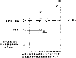
下面,基于图1对构成源极驱动器3的第n源极驱动器30进行说明。Next, the
正如该图所示,第n源极驱动器30具有作为锁存单元的输入锁存电路31、作为传送单元的移位寄存电路32、作为采样存储单元的采样存储电路33、作为扫描数据保持单元的保持存储电路34、作为电平移位单元的电平移位电路35、作为DA变换单元的DA变换电路36、作为输出单元的输出电路37、液晶驱动电压输出端子38(图中示出的R1、G1、B1~Rn、Gn、Bn端子),和灰度基准电压产生电路39,至此的结构和现有的结构图15中所示的是相同的。As shown in the figure, the
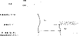
本实施方式还在现有的结构的基础上,进一步在保持存储电路34和电平移位电路35的连接信号间,增加了作为切换单元的显示数据/复位显示数据选择电路60,而且为了产生控制该显示数据/复位显示数据选择电路60的显示数据/复位显示数据选择控制信号DSCS,还增加了作为切换控制单元的显示数据/复位显示数据选择控制电路50和作为电源接通时间判断单元的电源接通复位电路40。而且,这些显示数据/复位显示数据选择电路60、显示数据/复位显示数据选择控制电路50以及电源接通复位电路40,构成为作为本发明的电源接通时间显示单元的电源接通时间显示部20。On the basis of the existing structure, this embodiment further adds a display data/reset display
下面,对电源接通时间显示部20中的各电路40·50·60进行详细说明。Next, each
首先,基于图4和图5对电源接通复位电路40的结构进行说明。如图4所示,电源接通复位电路40由电阻元件(R)41和电容元件(C)42以及反相缓冲电路43构成。First, the configuration of the power-on
在上述电源接通复位电路40中,如图5所示,由电阻元件(R)41和电容元件(C)42对电源接通时的电源波形暂时进行CR时间常数变换,相对原来的电源信号PW的电源接通波形生成呈使电源上升时间延迟的波形的时间常数变换信号TS,并输出到端子P1。将该波形输入到反相缓冲电路43,并生成电源接通复位信号RS。In the above-mentioned power-on
该电源接通复位信号RS利用反相缓冲电路43的输入信号即时间常数变换信号TS,以及反相缓冲电路43的门电位门限值,可以生成出相对原电源的接通在接通之后设置一定的复位期间用的信号。复位期可以通过改变电阻元件(R)41、电容元件(C)42以及反相缓冲电路43的元件参数的方式,来任意设定。通过本电源接通复位电路40可以按照电源接通时序,生成电源接通复位信号RS。The power-on reset signal RS uses the input signal of the inverting buffer circuit 43, that is, the time constant conversion signal TS, and the gate potential threshold value of the inverting buffer circuit 43, to generate A signal used during a certain reset period. The reset period can be set arbitrarily by changing the element parameters of the resistance element (R) 41 , the capacitance element (C) 42 and the inverting buffer circuit 43 . This power-on
下面,说明显示数据/复位显示数据选择控制电路50的结构。Next, the configuration of the display data/reset display data
如图6所示,显示数据/复位显示数据选择控制电路50可以将电源接通复位信号RS和控制信号CNT作为输入信号,由门组合电路部51生成显示数据/复位显示数据选择控制信号DSCS。电源接通复位信号RS是由前述的电源接通复位电路40生成的信号,控制信号CNT是从图2所示的控制器5提供给图1所示的第n源极驱动器30的控制信号。As shown in FIG. 6 , the display data/reset display data
对于上述的门组合电路部51,内部的逻辑结构根据显示数据/复位显示数据选择控制信号DSCS的生成时序不同。在本实施方式中,呈从电源接通之后到上述控制器5最初开始动作的期间,以写入复位数据这样的方式实施生成的电路构成形式。In the gate combination circuit section 51 described above, the internal logic structure differs depending on the generation timing of the display data/reset display data selection control signal DSCS. In the present embodiment, there is a circuit configuration form in which reset data is written in a period from when the power is turned on to when the controller 5 first starts to operate.
在上述显示数据/复位显示数据选择控制电路50中,如图7所示,呈通过在电源接通时由门组合电路部51接收由电源接通复位电路40生成的电源接通复位信号RS的方式,使显示数据/复位显示数据选择控制信号DSCS在时间T1被设置在施加电压“高(High)”的状态。In the above-mentioned display data/reset display data
而且,在控制信号CNT开始动作的时间T2,显示数据/复位显示数据选择控制信号DSCS被设置在施加电压“低(Low)”的状态。Furthermore, at time T2 when the control signal CNT starts to operate, the display data/reset display data selection control signal DSCS is set in the state of the applied voltage "Low".
由此,从电源接通之后到控制器5开始动作期间,可以由门组合电路部51生成作为输出脉冲的显示数据/复位显示数据选择控制信号DSCS。Thus, the display data/reset display data selection control signal DSCS can be generated as an output pulse by the gate combination circuit section 51 during the period from when the power is turned on to when the controller 5 starts to operate.
这里,上述控制器动作开始,将显示数据/复位显示数据选择控制信号DSCS设置在施加电压“低(Low)”的状态的时间T2,取决于后述的复位显示时间需要从电源接通到多长的期间结束。而且如果举例来说,对于从控制器动作开始直到多个脉冲的控制信号CNT输入后设置为施加电压“低(Low)”的状态的情况下等等,可以通过改变门组合电路部51的内部门组合结构的方式实施生成。Here, the above-mentioned controller starts to operate, and the time T2 for setting the display data/reset display data selection control signal DSCS to the state of the applied voltage "Low (Low)" depends on the reset display time described later. The long period ends. And if, for example, for the case where the applied voltage "Low" is set after the control signal CNT of a plurality of pulses is input from the start of the controller operation, etc., it can be changed by changing the internal gate combination circuit section 51 The way of department combination structure is implemented and generated.
下面,基于图8说明显示数据/复位显示数据选择电路60的结构。Next, the configuration of the display data/reset display
如该图所示,显示数据/复位显示数据选择电路60由1比特保持存储器电路61和数据选择电路62构成。这里的1比特保持存储器电路61相当于存储1比特的上述的图1中所示的保持存储电路34的显示数据的存储器,通常由触发器(Flip Flop)电路构成。As shown in the figure, the display data/reset display
数据选择电路62内的开关63·64相当于由模拟开关或者逻辑电平构成的2比特多路复用器(multiplexer)电路,通过将施加电压“高(High)”施加到栅极上的方式,可以表现为一个呈导通状态,其余呈截止状态的电路形式。而且,可以利用作为栅极电位的显示数据/复位显示数据选择控制信号DSCS,或者由反相器65进行反逻辑变换的信号对开关63·64进行开关控制。通过该动作,可以仅使开关63·64中的某一方导通。The
由该数据选择电路62选择并被输出的数据信号,是通过对由1比特保持存储器电路61采用通常的动作存储的显示数据,和复位期间显示的复位显示数据实施切换操作的方式,选择输出的信号。切换操作可以由显示数据/复位显示数据选择控制信号DSCS进行控制。The data signal selected and output by the
在上述显示数据/复位显示数据选择电路60中,当显示数据/复位显示数据选择控制信号DSCS的施加电压被设置为“低(Low)”时,开关63为导通状态,开关64为截止状态。由此,输出可以选择输出在1比特保持存储器电路61中锁存的数据。In the display data/reset display
另一方面,当显示数据/复位显示数据选择控制信号DSCS的施加电压被设置为“高(High)”时,开关63为截止状态,开关64为导通状态。由此,输出可以选择输出设定的复位显示数据。On the other hand, when the applied voltage of the display data/reset display data selection control signal DSCS is set to "High", the
对于复位显示数据的设定,可以通过预先设定相当于显示复位状态时的显示色的电位来进行对应。而且,可以通过在内部固定设定或者从外部供给的方式来进行该设定。The setting of the reset display data can be handled by setting in advance the potential corresponding to the display color in the display reset state. Also, the setting may be fixed inside or supplied from the outside.
换言之,可以使其具有利用在从电源接通到图2所示的控制器开始动作期间生成的显示数据/复位显示数据选择控制信号DSCS,仅在该显示数据/复位显示数据选择控制信号DSCS的施加电压被设置为“高(High)”期间,选择输出相对于复位显示的显示数据的功能。In other words, it is possible to use the display data/reset display data selection control signal DSCS generated during the period from when the power is turned on to when the controller shown in FIG. While the applied voltage is set to "High", select the function to output the display data for the reset display.
对于复位显示数据的设定,进行接近面板非点亮时的状态的变换。换言之,对于常亮模式(Normal White)的模块,可以设定为进行白显示或者接近白显示的显示数据。对于常黑模式(Normal Black)的模块,可以设定为进行黑显示或者接近黑显示的显示数据。For the setting of the reset display data, a transition close to the state when the panel is not lit is performed. In other words, for a module in Normal White mode, it can be set to display data for white display or close to white display. For the module of normal black mode (Normal Black), it can be set to display data in black display or close to black display.
通过将复位时的显示数据设定为这些状态,可以使面板电源接通时的显示固定在标准状态,从而可以使内部数据状态稳定,开始动作显示不发生紊乱。By setting the display data at reset to these states, the display when the panel power is turned on can be fixed at the standard state, so that the internal data state can be stabilized, and the start-up display will not be disturbed.
这里,对于上述复位显示数据的设定方法,给出了通过内部固定设定的方法以及通过从外部提供来进行设定的方法的具体结构形式。Here, with regard to the setting method of the above-mentioned reset display data, the specific structural forms of the method of setting by internal fixing and the method of setting by providing from outside are given.
首先,对于通过内部固定设定的情况给出两个实例。在本实施方式中,在电源接通之后的不定期间,数据固定在上述液晶面板1的标准非点亮状态的显示色。首先,在图9或者图10中示出的是第1实例。图9表示的是将复位期间的数据固定为“低(Low)”的情况。这种情况对于在常亮模式(Normal White)中为黑显示。另外,图10表示的是将复位期间的数据固定为“高(High)”的情况。这种情况对于在常亮模式(Normal White)中为白显示。First, two examples are given for the case of setting by internal fixation. In the present embodiment, the data is fixed at the display color of the standard non-lighting state of the above-mentioned
如图9或者图10所示,通过将开关64的基准电位固定为“低(Low)”或者“高(High)”的方式,可以固定为白数据、黑数据或者任意灰度数据。通过固定到内部电源或者基板电位的方式,可以使该固定在内部设定为“低(Low)”或者“高(High)”。As shown in FIG. 9 or FIG. 10 , by fixing the reference potential of the
另一方面,在图11或者图12中示出的是第2实例。图11表示的是将复位期间的数据固定为“低(Low)”的情况。这种情况对于在常亮模式(NormalWhite)中为黑显示。另外,图12表示的是将复位期间的数据固定为“高(High)”的情况。这种情况对于在常亮模式(Normal White)中为白显示。On the other hand, what is shown in FIG. 11 or FIG. 12 is the second example. FIG. 11 shows the case where the data in the reset period is fixed to "Low". In this case, it is displayed as black in the constant light mode (NormalWhite). In addition, FIG. 12 shows the case where the data in the reset period is fixed to "High". In this case, it is displayed as white in normal white mode.
如图11或者图12所示,可以将复位信号作为S(置位)触发器(flip-flop)或者R(复位)触发器(flip-flop)的置位信号或者复位信号使用,所以在复位信号期间可以直接使内部存储器为“低(Low)”或者“高(High)”的状态。As shown in Figure 11 or Figure 12, the reset signal can be used as the set signal or reset signal of the S (set) flip-flop or R (reset) flip-flop (flip-flop), so the reset During the signal period, the internal memory can be directly set to "Low" or "High" state.
而且,从外部设定非点亮状态的数据时,也可以采用如图9和图10所示的方法,从外部直接供给至复位数据固定部(在同一图形中用圆表示的部分)中。Moreover, when the data of the non-lighting state is set from the outside, the method shown in FIG. 9 and FIG. 10 can also be used to directly supply the reset data fixing part (the part indicated by a circle in the same figure) from the outside.
而且,本实施方式中的显示数据/复位显示数据选择电路60、显示数据/复位显示数据选择控制电路50以及电源接通复位电路40全部由逻辑电路构成。在通常的动作中,显示电位是根据复位显示数据变换的模拟电位,但本实施方式的特征在于,可以由数字部对电源接通状态的复位数据进行控制。因此,可以不采用从外部供给复位用的特殊电位、例如公共电位等。Furthermore, the display data/reset display
由于介于常规动作利用的DA变换电路36和输出电路37,所以由复位显示数据变换出的模拟显示电位可以采取选择相当于灰度显示电位中的一个的电位的结构。因此,相当于液晶驱动系统电路的,电平移位电路35、DA变换电路36、输出电路37和灰度基准电压发生电路39在实现本实施方式的结构中,可以保持现有的结构来实现。因此,能够实现电路尺寸的缩小和端子数的削减,而且能够抑制制造成本。Since the
换言之,本实施方式在保持存储电路34之后,可以用数字电路构成内部生成并切换电源接通之后作为面板非点亮状态的复位期间的显示数据/复位显示数据选择电路60、显示数据/复位显示数据选择控制电路50以及电源接通复位电路40。In other words, in this embodiment, after the
其结果是通过具备在面板电源接通时的一定期间内,在液晶面板1的非点亮状态(常黑模式时为黑,常亮模式时为白)的灰度数据中设置内部扫描信号,由源极驱动器输出被变换的灰度显示电平的电位的单元的方式,可以提供能够减轻或解决电源接通时的瞬间显示不正常问题的液晶驱动电路10b,以及具有该液晶驱动电路10b的液晶显示装置10。As a result, the internal scanning signal is set in the gradation data of the non-lighting state of the liquid crystal panel 1 (black in the normally black mode and white in the normally bright mode) for a certain period of time when the panel power is turned on, The way in which the source driver outputs the potential of the converted grayscale display level unit can provide a liquid crystal drive circuit 10b that can alleviate or solve the problem of abnormal display at the moment when the power is turned on, and a liquid crystal drive circuit 10b with the liquid crystal drive circuit 10b Liquid crystal display device 10 .
采用这种构成形式,在本实施方式的液晶驱动电路10b,电源接通时间显示部20为了可以在从液晶面板1的电源接通时刻到输出基于被输入的显示数据信号的灰度显示电平电压为止的一定期间内,将和基于该被输入的显示数据信号的灰度显示电平电压不同的灰度显示电平电压输出到多个液晶显示元件A,而预先另外设定灰度显示数字数据。With such a configuration, in the liquid crystal drive circuit 10b of the present embodiment, the power-on
因此,如果采用本实施方式,可以基本利用数字部,将电源接通时的显示不定期间固定为预先另外设定的灰度显示数字数据。由此,可以按数字方式设计电路结构,所以能够设计得比利用模拟电路的开关装置小得多。Therefore, according to the present embodiment, digital data can be displayed at a previously set gradation while fixing the display indefinite period when the power is turned on, basically by using the digital unit. As a result, the circuit configuration can be designed digitally, so it can be designed much smaller than a switching device using an analog circuit.
而且,DA变换电路36由于也利用现有的方式,所以不会对模拟输出的驱动能力产生影响。Furthermore, since the
其结果是,本发明能够提供出一种对于面板电源接通时的一定期间内产生的瞬间显示图像的紊乱,能够在将电路尺寸的增大控制在最小限度的条件下减轻该不正常显示问题的液晶驱动电路10b和显示元件驱动方法。As a result, the present invention can provide a method for temporarily displaying image disturbances that occur within a certain period of time when the power supply of the panel is turned on, and can reduce the abnormal display problem while controlling the increase in circuit size to a minimum. The liquid crystal driving circuit 10b and the display element driving method.
而且在本实施方式中,电源接通时间显示部20被配置在电平移位电路35之前。由此,可以基本利用数字部,将电源接通时的显示不定期间固定在预先另外设定的灰度显示数字数据。而且,其结果是,因为电平移位电路35之前的级中是由3~5V电源驱动的低电压驱动部,所以通过在该低电压驱动部中设置电源接通时间显示部20的方式,能够将电路的增大控制在最小限度。Furthermore, in the present embodiment, the power-on
而且,因为传送基于时钟信号的启动脉冲信号的移位寄存电路32、输入锁存电路31、采样存储电路33、电平移位电路35、DA变换电路36以及输出电路37,均可以采用和现有的显示元件驱动装置中相同的结构,所以还能够在维持原有面板周边部件的设置状态下,解决电源接通时的瞬间显示不正常的问题。Moreover, because the
而且,电源接通时间显示部20具有判断液晶面板1的电源是否已接通的电源接通复位电路40,切换预先另外设定的灰度显示数字数据和基于输入的显示数据信号的灰度显示数字数据的显示数据/复位显示数据选择电路60,和基于由电源接通复位电路40判断出的电源接通有无判断结果,控制上述显示数据/复位显示数据选择电路60中的预先另外设定的灰度显示数字数据和基于输入的显示数据信号的灰度显示数字数据之间的切换的显示数据/复位显示数据选择控制电路50。因此,本发明还能够提供出电源接通时间显示部20的具体结构。Furthermore, the power-on
而且,因为进行数-模变换的DA变换电路36一般来说,能够利用灰度显示基准电压产生电路39和调整放大器的结构产生出所期望的中间电压,所以电源接通时的显示电位可以依照现有的灰度变换方式实施输出。因此,能够实现电路尺寸的缩小和端子数的削减,且能够抑制制造成本。Moreover, because the
而且,在本实施方式的液晶驱动电路10b中,显示数据/复位显示数据选择电路60设置在为了可以保持采样存储电路33的输出而设置的保持存储电路34的后级,且设置在电平移位电路35之前。Furthermore, in the liquid crystal drive circuit 10b of the present embodiment, the display data/reset display
因此,对于预先另外设定的显示元件驱动电位的生成,在本发明中,对将显示数据变换为模拟电位的现有液晶驱动装置,试图通过模拟变换前的显示数据的切换处理来解决。因此,能够在不增大电路尺寸的条件下很容易地实现对上述问题的解决。Therefore, in the present invention, it is attempted to solve the problem of generating the display element driving potential separately set in advance by switching the display data before analog conversion for the conventional liquid crystal driving device that converts the display data into an analog potential. Therefore, the solution to the above-mentioned problems can be easily realized without increasing the size of the circuit.
而且,在本实施方式的液晶驱动电路10b和显示元件驱动方法中,显示数据/复位显示数据选择控制电路50可以通过切换到作为预先另外设定的灰度显示数字数据的、接近显示元件非点亮状态的显示数据的方式进行控制。这里,接近显示元件非点亮状态的显示数据可以为在常黑模式时为黑数据,在常亮模式时为白数据。由此,在电源接通时能够进行维持电源关闭状态的显示。Furthermore, in the liquid crystal driving circuit 10b and the display element driving method of the present embodiment, the display data/reset display data
而且,在本实施方式的液晶驱动电路10b中,显示元件可以是液晶显示元件A。因此,在驱动液晶显示元件A的液晶驱动电路10b中,对于面板电源接通时的一定期间内产生的瞬间显示图像的紊乱,能够在将电路尺寸的增大控制在最小限度的条件下减轻该显示不正常问题。Furthermore, in the liquid crystal drive circuit 10b of this embodiment, the display element may be a liquid crystal display element A. As shown in FIG. Therefore, in the liquid crystal drive circuit 10b for driving the liquid crystal display element A, the disorder of the displayed image that occurs momentarily during a certain period when the panel power is turned on can be alleviated while minimizing the increase in circuit size. Display abnormal problem.
而且,本实施方式的液晶显示装置10具有上述液晶驱动电路10b。其结果是,本发明还能够提供出具备对于面板电源接通时的一定期间内产生的瞬间显示图像的紊乱,能够在将电路尺寸的增大控制在最小限度的条件下减轻该不正常显示问题的液晶驱动电路10b的液晶显示装置10。Furthermore, the liquid crystal display device 10 of the present embodiment includes the liquid crystal drive circuit 10 b described above. As a result, the present invention can also provide a device capable of responding to transient display image disturbances that occur during a certain period of time when the panel power is turned on, and can reduce this abnormal display problem while keeping the increase in circuit size to a minimum. The liquid crystal display device 10 of the liquid crystal driving circuit 10b.
如上所述,在本发明的显示元件驱动装置中,切换单元可以设置在为了可以保持上述采样单元的输出而设置的扫描数据保持单元的后级,且设置在上述电平移位单元的前级。As described above, in the display element driving device of the present invention, the switching unit may be provided at a subsequent stage of the scanning data holding unit provided to hold the output of the sampling unit, and at a preceding stage of the level shifting unit.
如果采用上述发明,切换单元设置在为了可以保持上述采样单元的输出而设置的扫描数据保持单元的后级,且设置在上述电平移位单元的前级。According to the above invention, the switching unit is provided at the subsequent stage of the scanning data holding unit provided to hold the output of the sampling unit, and is provided at the preceding stage of the level shifting unit.
因此,对于预先另外设定的显示元件驱动电位的生成,本发明对将显示数据变换为模拟电位的现有液晶驱动装置,试图通过模拟变换前的显示数据的切换处理来解决。因此,能够在不增大电路尺寸的条件下很容易地实现对上述问题的解决。Therefore, the present invention attempts to solve the problem of generating display element drive potentials separately set in advance by switching display data before analog conversion in conventional liquid crystal drive devices that convert display data into analog potentials. Therefore, the solution to the above-mentioned problems can be easily realized without increasing the size of the circuit.
而且,在本发明的显示元件驱动装置中,切换控制单元可以通过切换到作为预先另外设定的灰度显示数字数据的、接近显示元件非点亮状态的显示数据的方式进行控制。Furthermore, in the display element driving device of the present invention, the switching control means may perform control by switching to display data close to the non-lighted state of the display element as gray scale display digital data set separately in advance.
而且,在本发明的显示元件驱动方法中,使用作为预先另外设定的灰度显示数字数据的、接近显示元件非点亮状态的显示数据。Furthermore, in the display element driving method of the present invention, display data close to the non-lighted state of the display element is used as digital data for gradation display separately set in advance.
如果采用上述发明,切换控制单元可以按照能切换到作为预先另外设定的灰度显示数字数据的、接近显示元件非点亮状态的显示数据的方式进行控制。这里,接近显示元件非点亮状态的显示数据可以为在常黑模式时为黑的数据,在常亮模式时为白的数据。According to the above invention, the switching control means can perform control in such a manner as to be able to switch to display data close to the non-lighted state of the display element, which is separately set grayscale display digital data in advance. Here, the display data close to the non-lighting state of the display element may be black data in the normally black mode and white data in the normally bright mode.
由此,在电源接通时能够进行维持电源关闭状态的显示。Thereby, when the power is turned on, it is possible to perform a display that maintains the power-off state.
而且,在本发明的显示元件驱动装置中,显示元件可以是液晶显示元件。Furthermore, in the display element driving device of the present invention, the display element may be a liquid crystal display element.
如果采用上述发明,还能够提供出在驱动液晶显示元件的显示元件驱动装置中,对于面板电源接通时的一定期间内产生的瞬间显示图像的紊乱,能够在将电路尺寸的增大控制在最小限度的条件下减轻该不正常显示问题的显示元件驱动装置。According to the above-mentioned invention, it is also possible to provide a display element driving device for driving a liquid crystal display element, which can minimize the increase in the circuit size for the disorder of the displayed image that occurs within a certain period of time when the panel power is turned on. A display device driving device that alleviates the problem of abnormal display under limited conditions.
而且,在发明的详细说明部分中给出的具体实施方式或者实施例只是为了使本发明的技术内容变得明确而容易理解,本发明并不仅仅限定于这些具体例子进行的狭义解释,可以在本发明的宗旨和下面记载的权利要求书的范围内进行各种变型实施。Moreover, the specific implementation methods or examples given in the detailed description of the invention are only to make the technical content of the present invention clear and easy to understand. The present invention is not limited to the narrow interpretation of these specific examples, and can be found Various modified implementations are possible within the gist of the present invention and the scope of the claims described below.
Claims (10)
Applications Claiming Priority (3)
| Application Number | Priority Date | Filing Date | Title |
|---|---|---|---|
| JP2004291888 | 2004-10-04 | ||
| JP2004291888A JP4290627B2 (en) | 2004-10-04 | 2004-10-04 | Display element driving apparatus, display device including the display element driving apparatus, and display element driving method |
| JP2004-291888 | 2004-10-04 |
Publications (2)
| Publication Number | Publication Date |
|---|---|
| CN1758322A true CN1758322A (en) | 2006-04-12 |
| CN100419844C CN100419844C (en) | 2008-09-17 |
Family
ID=36125048
Family Applications (1)
| Application Number | Title | Priority Date | Filing Date |
|---|---|---|---|
| CNB2005101165568A Expired - Fee Related CN100419844C (en) | 2004-10-04 | 2005-09-30 | Display element driving device, display device having same, and driving method |
Country Status (5)
| Country | Link |
|---|---|
| US (1) | US7633476B2 (en) |
| JP (1) | JP4290627B2 (en) |
| KR (1) | KR100742804B1 (en) |
| CN (1) | CN100419844C (en) |
| TW (1) | TWI317115B (en) |
Families Citing this family (26)
| Publication number | Priority date | Publication date | Assignee | Title |
|---|---|---|---|---|
| JP4075880B2 (en) * | 2004-09-29 | 2008-04-16 | セイコーエプソン株式会社 | Electro-optical device, data line driving circuit, signal processing circuit, and electronic device |
| JP4777050B2 (en) * | 2005-11-21 | 2011-09-21 | 東芝モバイルディスプレイ株式会社 | Display panel control circuit |
| KR100796136B1 (en) * | 2006-09-13 | 2008-01-21 | 삼성에스디아이 주식회사 | Organic light emitting display device and driving method thereof |
| JP2008116917A (en) * | 2006-10-10 | 2008-05-22 | Seiko Epson Corp | Gate driver, electro-optical device, electronic apparatus, and driving method |
| JP4837522B2 (en) * | 2006-10-19 | 2011-12-14 | 株式会社 日立ディスプレイズ | Display device drive circuit |
| JP5508662B2 (en) | 2007-01-12 | 2014-06-04 | 株式会社半導体エネルギー研究所 | Display device |
| TW200847097A (en) * | 2007-05-18 | 2008-12-01 | Gigno Technology Co Ltd | Electronic paper apparatus and its driving circuit and manufacturing method |
| WO2009011150A1 (en) * | 2007-07-18 | 2009-01-22 | Sharp Kabushiki Kaisha | Display device and its driving method |
| TWI395196B (en) * | 2008-01-14 | 2013-05-01 | 奕力科技股份有限公司 | Gamma voltage driving circuit and method for generating gamma voltage |
| US20100315405A1 (en) * | 2008-04-16 | 2010-12-16 | Noriyuki Tanaka | Driving circuit for liquid crystal display device |
| TWI404011B (en) * | 2009-03-18 | 2013-08-01 | Pervasive Display Co Ltd | Non-volatile display module and non-volatile display apparatus |
| TWI489430B (en) | 2010-01-11 | 2015-06-21 | Novatek Microelectronics Corp | Driving apparatus of display |
| KR101111529B1 (en) * | 2010-01-29 | 2012-02-15 | 주식회사 실리콘웍스 | Source driver circuit of liquid crystal display |
| TWI422226B (en) * | 2010-07-02 | 2014-01-01 | Beyond Innovation Tech Co Ltd | Processing apparatus of video signal |
| TWI582743B (en) * | 2011-05-03 | 2017-05-11 | 矽工廠股份有限公司 | Liquid crystal panel driving circuit for display stabilization |
| CN102194431B (en) * | 2011-05-19 | 2013-12-25 | 华映光电股份有限公司 | Driving system of liquid crystal display |
| US8982027B2 (en) * | 2011-07-28 | 2015-03-17 | Shenzhen China Star Optoelectronics Technology Co., Ltd. | LCD drive circuit and driving method for scanning at least two adjacent scan lines simultaneously |
| CN102693705A (en) * | 2012-01-18 | 2012-09-26 | 矽创电子股份有限公司 | Panel driving circuit |
| US9230502B2 (en) * | 2012-02-13 | 2016-01-05 | Semiconductor Energy Laboratory Co., Ltd. | Display device having blocking circuit for extracting start pulse from signal |
| US10115357B2 (en) | 2012-12-18 | 2018-10-30 | Apple Inc. | Display with soft-transitioning column driver circuitry |
| DE112014002915B4 (en) * | 2013-06-21 | 2018-02-01 | Yazaki Corporation | display device |
| KR20150088598A (en) * | 2014-01-24 | 2015-08-03 | 삼성디스플레이 주식회사 | Data driver and display apparatus having the same and method of driving display panel using the same |
| CN106656645B (en) * | 2015-10-29 | 2020-01-03 | 北京北方华创微电子装备有限公司 | Monitoring device of point-to-point communication equipment and monitoring system with same |
| KR102323513B1 (en) * | 2017-07-20 | 2021-11-08 | 삼성디스플레이 주식회사 | Display device and method of driving the same |
| TWI725650B (en) * | 2019-05-17 | 2021-04-21 | 友達光電股份有限公司 | Source driver device |
| TWI812196B (en) * | 2022-04-29 | 2023-08-11 | 宏碁股份有限公司 | Display device |
Family Cites Families (26)
| Publication number | Priority date | Publication date | Assignee | Title |
|---|---|---|---|---|
| JPH02272490A (en) * | 1989-04-14 | 1990-11-07 | Hitachi Ltd | Liquid crystal display device and power supply device for liquid crystal display device |
| JPH04204993A (en) | 1990-11-30 | 1992-07-27 | Sharp Corp | Driving circuit for display device |
| JPH04291227A (en) * | 1991-03-19 | 1992-10-15 | Toshiba Corp | Power supply controller for display |
| JPH07170986A (en) * | 1993-11-05 | 1995-07-11 | Hayashibara Biochem Lab Inc | DNA encoding a polypeptide, recombinant DNA containing the DNA, and transformant |
| JPH08146379A (en) | 1994-11-25 | 1996-06-07 | Hitachi Ltd | LCD drive circuit |
| JP3544580B2 (en) | 1995-04-28 | 2004-07-21 | 株式会社日立製作所 | Matrix panel display device, matrix panel control device, scanning voltage driving circuit and data voltage driving circuit thereof |
| JP3433337B2 (en) * | 1995-07-11 | 2003-08-04 | 日本テキサス・インスツルメンツ株式会社 | Signal line drive circuit for liquid crystal display |
| JPH09230832A (en) | 1996-02-27 | 1997-09-05 | Casio Comput Co Ltd | Electronic device with trimming function |
| JPH10232652A (en) | 1997-02-21 | 1998-09-02 | Hitachi Ltd | Liquid crystal display device and information processing system |
| JPH10319916A (en) | 1997-05-19 | 1998-12-04 | Matsushita Electric Ind Co Ltd | Liquid crystal display |
| CN1115660C (en) * | 1998-03-17 | 2003-07-23 | 明碁电脑股份有限公司 | Liquid crystal monitor with liquid crystal display panel protection circuit |
| JP2001013478A (en) | 1999-06-28 | 2001-01-19 | Fujitsu Ltd | Source driver for liquid crystal display device and liquid crystal display device using the same |
| JP3526244B2 (en) * | 1999-07-14 | 2004-05-10 | シャープ株式会社 | Liquid crystal display |
| JP3495960B2 (en) | 1999-12-10 | 2004-02-09 | シャープ株式会社 | Gray scale display reference voltage generating circuit and liquid crystal driving device using the same |
| KR20040010768A (en) * | 2001-06-20 | 2004-01-31 | 마츠시타 덴끼 산교 가부시키가이샤 | Image display and its drive method |
| JP3795361B2 (en) * | 2001-09-14 | 2006-07-12 | シャープ株式会社 | Display driving device and liquid crystal display device using the same |
| KR100806903B1 (en) * | 2001-09-27 | 2008-02-22 | 삼성전자주식회사 | Liquid crystal display and driving method thereof |
| KR100767377B1 (en) * | 2001-09-28 | 2007-10-17 | 삼성전자주식회사 | Organic EL display panel and organic EL display device having same |
| JP2003280615A (en) * | 2002-01-16 | 2003-10-02 | Sharp Corp | Gray scale reference voltage generating circuit and liquid crystal display device using the same |
| JP3926651B2 (en) * | 2002-01-21 | 2007-06-06 | シャープ株式会社 | Display drive device and display device using the same |
| JP4269582B2 (en) | 2002-05-31 | 2009-05-27 | ソニー株式会社 | Liquid crystal display device, control method thereof, and portable terminal |
| JP4759906B2 (en) | 2002-12-12 | 2011-08-31 | ソニー株式会社 | Liquid crystal display device, control method thereof, and portable terminal |
| KR100493622B1 (en) * | 2003-03-04 | 2005-06-10 | 엘지전자 주식회사 | Plasma Display Panel |
| TW594662B (en) | 2003-06-03 | 2004-06-21 | Chunghwa Picture Tubes Ltd | Method for restraining noise when flat display turn on/off |
| US7755589B2 (en) * | 2003-06-03 | 2010-07-13 | Chunghwa Picture Tubes, Ltd. | Noise suppressing method for flat panel display |
| US7199774B2 (en) * | 2004-02-17 | 2007-04-03 | Au Optronics Corp. | Liquid crystal display |
-
2004
- 2004-10-04 JP JP2004291888A patent/JP4290627B2/en not_active Expired - Fee Related
-
2005
- 2005-09-28 TW TW094133787A patent/TWI317115B/en not_active IP Right Cessation
- 2005-09-30 CN CNB2005101165568A patent/CN100419844C/en not_active Expired - Fee Related
- 2005-10-03 US US11/240,464 patent/US7633476B2/en not_active Expired - Fee Related
- 2005-10-04 KR KR1020050092825A patent/KR100742804B1/en not_active Expired - Fee Related
Also Published As
| Publication number | Publication date |
|---|---|
| JP2006106293A (en) | 2006-04-20 |
| TWI317115B (en) | 2009-11-11 |
| TW200625235A (en) | 2006-07-16 |
| CN100419844C (en) | 2008-09-17 |
| KR100742804B1 (en) | 2007-07-25 |
| US7633476B2 (en) | 2009-12-15 |
| JP4290627B2 (en) | 2009-07-08 |
| US20060071892A1 (en) | 2006-04-06 |
| KR20060051992A (en) | 2006-05-19 |
Similar Documents
| Publication | Publication Date | Title |
|---|---|---|
| CN1758322A (en) | Display element drive unit, display device including the same, and display element drive method | |
| CN1267880C (en) | Display driving circuit, display faceboard, display device and display driving method | |
| CN1624737A (en) | Display device, driver circuit therefor, and method of driving same | |
| CN1267881C (en) | Liquid crystal display device | |
| CN1284131C (en) | Driving circuit, photoelectric device and driving method | |
| CN1241164C (en) | Display and drive circuit for display | |
| CN1551076A (en) | Image display apparatus | |
| CN1514426A (en) | image display device | |
| CN1540607A (en) | Driving circuit for color image display and display device having same | |
| CN101075417A (en) | Displaying apparatus using data line driving circuit and data line driving method | |
| CN1620681A (en) | Electronic device drive method, electronic device, semiconductor integrated circuit, and electronic apparatus | |
| CN1284132C (en) | Driving circuit, photoelectric device and driving method | |
| CN1547730A (en) | Liquid crystal display device, control method thereof and mobile terminal | |
| CN100351892C (en) | Liquid-crystal driver and liquid-crystal display | |
| CN1658271A (en) | Liquid crystal display device | |
| CN1503216A (en) | Driving circuit, photoelectric device and driving method thereof | |
| CN1617209A (en) | Driving method of pixel circuit, pixel circuit and electronic device | |
| CN1811882A (en) | Organic electroluminescent display device and method of driving the same | |
| CN1637497A (en) | Liquid crystal display and driving method thereof | |
| CN1082194C (en) | Liquid crystal electro-optic device | |
| CN1801311A (en) | Method of driving display device and display device for performing the same | |
| CN1808534A (en) | Display device and mobile terminal | |
| CN1700061A (en) | Liquid crystal display device and method of driving such a display device | |
| CN101051448A (en) | Semiconductor integrated circuit device used in data line driver of plane type display apparatus | |
| CN1504987A (en) | LCD driver |
Legal Events
| Date | Code | Title | Description |
|---|---|---|---|
| C06 | Publication | ||
| PB01 | Publication | ||
| C10 | Entry into substantive examination | ||
| SE01 | Entry into force of request for substantive examination | ||
| C14 | Grant of patent or utility model | ||
| GR01 | Patent grant | ||
| CF01 | Termination of patent right due to non-payment of annual fee |
Granted publication date: 20080917 Termination date: 20140930 |
|
| EXPY | Termination of patent right or utility model |