JP3544580B2 - Matrix panel display device, matrix panel control device, scanning voltage driving circuit and data voltage driving circuit thereof - Google Patents
Matrix panel display device, matrix panel control device, scanning voltage driving circuit and data voltage driving circuit thereof Download PDFInfo
- Publication number
- JP3544580B2 JP3544580B2 JP10663995A JP10663995A JP3544580B2 JP 3544580 B2 JP3544580 B2 JP 3544580B2 JP 10663995 A JP10663995 A JP 10663995A JP 10663995 A JP10663995 A JP 10663995A JP 3544580 B2 JP3544580 B2 JP 3544580B2
- Authority
- JP
- Japan
- Prior art keywords
- signal
- voltage
- data
- mode
- scanning
- Prior art date
- Legal status (The legal status is an assumption and is not a legal conclusion. Google has not performed a legal analysis and makes no representation as to the accuracy of the status listed.)
- Expired - Fee Related
Links
Images


Landscapes
- Liquid Crystal (AREA)
- Liquid Crystal Display Device Control (AREA)
- Transforming Electric Information Into Light Information (AREA)
Description
【0001】
【産業上の利用分野】
本発明は、マトリクス表示装置に関し、特に単純マトリクス形液晶表示装置において、低消費電力で駆動可能な液晶表示装置およびその駆動回路に関するものである。
【0002】
【従来の技術】
単純マトリクス形の液晶パネルを有する液晶表示装置の駆動方式として、工業調査会から出版されている[液晶の最新技術、P.106〜P.107]に記載された電圧平均化駆動方式が広く採用されている。この方式では、液晶パネルの行に対応する走査電極には、1本ずつ順次に選択走査電圧を1走査期間ずつ印加し、1フレーム期間で全ての走査電極を走査すると再び同じ動作を繰り返す。液晶パネルの列に対応するデータ電極には、表示データの値に対応したデータ電圧を非選択走査電圧レベルを中心に印加する。さらに、液晶印加電圧の極性を一定の期間毎に反転する交流化動作を行う。
【0003】
一方、単純マトリクス形の液晶パネルを有する液晶表示装置の駆動方式には特開平6−67628に記載された複数ライン選択駆動方式がある。この方式において、液晶パネルの行に対応する走査電極には、複数本ずつ直交関数(例えばウォルシュ関数)に対応した選択走査電圧を順次印加し、1フレーム期間と呼ばれる期間で全ての走査電極を走査すると、再び同じ動作を繰り返す。液晶パネルの列に対応するデータ電極には、選択走査されたラインにおける直交関数の値および表示データの値との一致数に対応したデータ電圧を印加する。
【0004】
ここで、電圧平均化法は交流化動作時においては、データドライバと走査ドライバの電圧を走査ドライバの選択電圧付近までレベルシフトするため、出力振幅は等しくなり、その値は走査電極数Nを用いて、
【0005】
【数1】

で与えられる。これに対し、複数ライン選択駆動方式におけるデータドライバと、走査ドライバの出力振幅は、それぞれ、選択ライン数mと走査電極数Nを用いて
【0007】
【数2】
【数3】
で与えられる。ここで、Voffは表示オフ時に液晶に印加される電圧実効値であり、通常2.0〜2.5[V]の値をとる。複数ライン選択駆動方式ではライン数mの値が比較的小さい場合、例えばm=1、N=240、Voff=2.2[V]にすると数2からデータドライバの振幅は約3.3[V]となり、電圧平均化法におけるデータドライバの振幅(数1から、約27[V])と比較してデータドライバの振幅が大幅に小さくなる。ドライバの電力はデータ側が走査側よりも大きいことを考慮すると、複数ライン選択駆動方式は電圧平均化法に比べて低消費電力な駆動方式であるといえる。
【0010】
【発明が解決しようとする課題】
複数ライン選択駆動方式において、選択ライン数mが小さい値の場合、データドライバの出力振幅は小さいものの、走査ドライバの振幅は大きくなる。この走査ドライバの振幅は走査電極数Nが多くなる程大きくなるため、走査電極数Nの値によっては、耐圧の問題から走査ドライバの製造が困難になるという課題がある。
【0011】
一方、同時選択走査ライン数mが大きい値の場合、数2、数3から、選択走査電圧と表示データ電圧の振幅レベルの差は減少することが分かる。したがって、この場合には、走査電極数Nが多くなっても走査ドライバの耐圧は十分製造可能な範囲になる。しかし、その反面、表示データ電圧の振幅が増大するため、データドライバに必要とされる耐圧も増大する。この耐圧が5Vを越えた場合、現在広く採用されているロジックプロセスを使用することができなくなり、製造コストが急激に増大するという課題がある。
【0012】
さらに、同時選択走査ライン数mの増加に伴い、直交関数と表示データの一致数の演算を行う回路の規模が増大し、回路の消費電力及び実現コストが増大するという課題がある。
【0013】
そこで、本発明は、液晶パネルの走査電極数N等に応じて、同時選択走査ライン数mを選択することができるマトリクスパネル表示装置とそれに含まれる駆動回路を提供することを目的とする。
【0014】
【課題を解決するための手段】
上述した課題を解消するためには、まず走査電極数Nに応じ、走査ドライバの耐圧をクリアできる選択ライン数mを選定することが必要となる。これと同時にデータドライバの耐圧を、製造コストの低いプロセスの最大出力電圧以下にすることが重要である。
【0015】
そこで、走査ライン数Nおよび選択ライン数mに対する、走査ドライバ、データドライバの耐圧の関係を、表示オフ状態で液晶に印加される電圧実効値を2.3Vとして求めた。これを図2に示す。図2において走査ドライバの耐圧の限界を例えば50Vとすると、m=1の場合N=245行まで実現可能、m=2の場合N=500行まで実現可能、さらにm=3ではN=600以上まで実現可能であることが分かる。一方、データドライバの耐圧に着目すると、例えば現在広く採用されているロジック用プロセスが可能な5V以下となる条件は、m=2以下の場合である。したがって、例えば、コンピュータディスプレイの標準的な解像度の1つである640列×480行の表示を行うには、m=1、またはm=2として640列×240行の液晶パネルを2画面構成で駆動させればよい。また、標準的な解像度の1つである800列×600行の表示を行うには、m=2として800列×300行の液晶パネルを2画面構成で駆動させればよい。
【0016】
以上の点に着目し、本発明の液晶表示装置は、液晶パネルの解像度に応じて、同時選択走査ライン数mを、例えばm=1とm=2の場合で選択できるような、走査ドライバ、データドライバおよび電源回路を設けた。さらに、本発明の走査ドライバには直交関数を発生する回路を内蔵し、データドライバには直交関数と表示データの一致数の演算を行う回路を内蔵した。これにより従来液晶コントローラとの互換性を保ち、実現コスト、消費電力の増大を防ぐことが可能となる。なお、同時選択走査ライン数mが“1”の場合は、直交関数を必要とせず、電圧平均化方式と同様にデータドライバは表示データに応じた電圧を出力することになる。このため、液晶の劣化を防ぐ交流化動作が必要となるため、交流化信号を生成する回路を設けた。
【0017】
【作用】
本発明のマトリクス表示装置は、複数ライン駆動方式に基づいたものであるため従来の電圧平均化駆動方式に比べて消費電力を小さくでき、また、走査ラインの選択数mを選択することができるため、走査ドライバおよびデータドライバの出力範囲内で走査ライン数Nの大きな種液晶パネルを駆動することができる。さらに、直交関数の発生手段および表示データと該直交関数との演算機能を内蔵しているため、走査ラインの選択数mにかかわらず従来の液晶コントローラをそのまま使用することができる。
【0018】
【実施例】
<第1実施例>
以下、本発明の第1の実施例を、図1および図3〜図14を用いて説明する。
【0019】
図1は本発明の第1実施例に係る液晶表示装置の構成を示すブロック図である。
【0020】
図1において、101は液晶パネルであり、本実施例では液晶パネル101は縦iドット、横jドットのマトリクス表示が可能である。102は本発明の走査ドライバ、103は本発明のデータドライバである。104は8ビットのパラレルデータである表示データD7〜D0であり、105は表示データ104の取り込みに用いられるデータラッチクロックCL2である。106はラインクロックCL1であり、ラインクロック106の1周期(1ライン走査期間)に1ライン分の表示データ104が送られる。107は先頭ラインクロックFLMであり、先頭ラインクロック107の1周期(1フレーム期間)にi回のライン走査が行われる。108は表示オフ制御信号DISPOFFで、この信号が”ロー”の時、液晶パネル101の表示が停止される。なお、これら表示データ104および同期信号群105〜108は、従来から用いられている液晶コントローラ109より供給される。
【0021】
110,111は液晶ドライバ103,102の動作をそれぞれに制御するコントロール信号群である。112は液晶印加電圧の交流化を図るためのタイミング信号を生成する交流化信号発生回路であり、113は交流化信号発生回路112により生成される交流化M信号である。このM信号113は、数10走査期間毎に“ハイ”と“ロー”が切り替わるように生成される。114および115は液晶パネルのドライバおよび交流化信号発生回路112を駆動させるための電源電圧群であり、116は電圧群114および115を生成する電源回路である。117,118は電源電圧群114および115の基となる外部電源電圧VCC,VEE、119は液晶駆動電圧群の電圧レベルの調節に用いれられる電圧VCONであり、本実施例ではこれら電圧117〜119は表示システム本体120から供給される。
【0022】
以下、図1に示す液晶表示装置の各ブロックの構成および動作について図3〜図13を用いて説明する。
【0023】
まず、本発明の電源回路116の一例について図3を用いて説明する。図3は電源回路116の構成図であり、301〜303はそれぞれ走査ドライバ電源電圧VyH,VyC,VyLであり、304〜306はそれぞれ液晶駆動用走査電圧Vy0〜Vy2である。これらの電圧301〜306は走査ドライバ102へ供給される。また、307,308はそれぞれデータドライバ電源電圧VxH,VxL、309〜311はそれぞれ液晶駆動用データ電圧Vx0〜Vx2であり、これらの電圧307〜311はデータドライバ103へ供給される。
【0024】
走査ドライバ電源電圧301〜303、液晶駆動用走査電圧のVy0電圧304,Vy2電圧306、およびデータドライバ電源電圧307,308は、それぞれDC−DCコンバータ312により生成される。また、液晶駆動用データ電圧309〜311および液晶駆動用走査電圧のVy1電圧305は、走査ドライバ電源電圧のVyH電圧301とVyL電圧303間の電圧を抵抗R1〜R4で分圧することにより生成される。なお、抵抗R1〜R4間には、
数4
R1=R4、
R2=R3、
という関係がある。また、上記各電圧間には、
数5
VyH=Vy2>Vy1>VyL=Vy0、
Vy2−Vy1=Vy1−Vy0、
VxH>Vx2>Vx1>Vx0>VxL、
Vx2−Vx1=Vx1−Vx0、
Vy1=Vx1
の関係がある。なお、Vx2電圧311とVx0電圧309の電位差は、数2で与えられ、Vy2電圧306とVy0電圧304の電位差は、数3で与えられる。ここで、液晶駆動用データ電圧309〜311および液晶駆動用走査電圧のVy1電圧305は、オペアンプを用いたボルテージフォロア回路313を介して出力される。また、各オペアンプはデータドライバ電源電圧307,308を電源としている。
【0025】
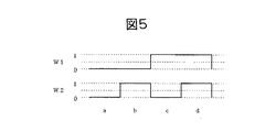
次に本発明の走査ドライバ102の構成および動作について図4〜図8を用いて説明する。図4は本発明の走査ドライバ102の構成図であり、図5は走査ドライバ102で生成される直交関数の一例を示す図、図6は走査ドライバ102で生成される直交関数の組合せ例を示す図、図7は走査ドライバ102の動作を説明するための図、図8は走査ドライバ102の入出力信号のタイミングチャ−トである。
【0026】
本発明の走査ドライバ102は、図4に示すように、入力信号レベルシフタ401、出力信号レベルシフタ402、直交関数発生回路403、直交関数ラッチ回路404、クロック制御回路405、走査ラインセレクタ406、液晶電圧レベルシフタ407、液晶電圧デコーダ408、液晶電圧セレクタ409で構成されている。また、410は1ライン選択走査駆動と2ライン選択走査駆動の内のいずれかのモードを指示するMODE信号、411,412は各1ビットの直交関数W1信号,W2信号、413はライン転送クロックCL3信号である。
【0027】
入力信号レベルシフタ401は、VccとGNDレベルの入力信号群を、内部ロジック駆動用電圧であるVyCとVyLレベルにレベルシフトするための回路であり、出力信号レベルシフタ402は、反対に内部ロジックで生成されるVyCとVyLレベルの信号群を、VccとGNDレベルの信号群にレベルシフトするための回路である。これらのレベルシフトには電源回路116より供給される電圧群115が用いられる。
【0028】
直交関数発生回路403は、直交関数を発生する部分であり、入力されるMODE信号410が”ロー”の場合1ライン選択走査駆動モード(以下、単に1ライン駆動モードという)となる。このモードにおいては、直交関数発生回路403は入力される交流化M信号113をW1信号として他のブロックへ転送する。一方、MODE信号410が”ハイ”の場合、直交関数発生回路403は2ライン選択走査駆動モード(以下、2ライン駆動モードという)となり、ファーストラインマーカFLM信号107のカウント値、およびラインクロックCL1信号106のカウント値に基づき、W0信号411、W1信号412、および走査ライン転送クロックCL3信号413を生成して出力する。
【0029】
この直交関数発生回路403の内部で生成される直交関数の一例を図5、図6を用いて説明する。図5に示すように、直交関数W1信号411とW2信号412の組合せには(W1,W2)=(0,0)、(0,1)、(1,0)、(1,1)の4通りがある。図6はFLM信号107およびCL1信号106を8進でカウントした場合に、どのカウント値でどの組合せ(図5におけるa〜d)が選択されるかを示している。図において、例えばFLM信号107のカウント値が十進表示で”2”、CL1信号106のカウント値が”1”の場合、(W1,W2)=(0,1)が直交関数として出力され、FLM信号107のカウント値が”7”、CL1信号106のカウント値が”5”の場合、(W1,W2)=(0,0)が出力される。
【0030】
また、直交関数発生回路403は、1ライン駆動モードの場合は内部で生成される走査ライン転送クロックCL3信号412をそのままCL1信号106として出力し、2ライン駆動モードの場合はCL3信号を2分周した信号ををCL1信号106として出力する。なお、直交関数W1,W2は液晶電圧レベルシフタ407により高電圧に変換されるが、その前に出力同期を図るため、直交関数ラッチ回路404にてCL1信号106のタイミングでラッチされる。なお、直交関数発生回路403内部で生成される直交関数の組合せは図6に示したものに限られたわけではなく、直交性を有するものであればよい。
【0031】
クロック制御回路405は、1ライン駆動モードの場合はFLM信号107をそのまま走査基準データとして走査ラインセレクタ406に転送し、2ライン駆動モードの場合はFLM信号107をCL1信号106に従って2走査期間だけ遅らせてたものを走査基準データとして転送する。
【0032】
走査ラインセレクタ406は液晶電圧出力のチャンネル数分(i個)のシフト回路からなる。ロック制御部405からの走査基準データは、このシフト回路においてラインクロックCL1信号106に従ってシフトされ、その結果がライン選択信号S1〜Siとして出力される。すなわち、ラインの選択(走査)を示す状態が信号S1からSiにかけて順次推移し、1フレーム期間ですべての選択が終了する。なお、表示オフ制御DISPOFF信号108が”ロー”の場合はこの回路はシフト動作を停止してリセット状態となる。
【0033】
液晶電圧レベルシフタ407は、内部ロジック電源電圧レベルの信号を液晶駆動用の高電圧VyHとVyLレベルの電圧に昇圧する回路である。この昇圧には電源回路116より供給される電圧群115が用いられる。
【0034】
液晶電圧デコーダ408および液晶電圧セレクタ409は、ライン選択信号S1〜Siと直交関数の組合せに従い、3レベルの液晶駆動用走査電圧Vy0〜Vy2の中から1レベルを選択して、その結果を走査駆動電圧Y1〜Yiとして出力する。例えば図7に示すように、直交関数が”0”の時、選択信号が”選択”(走査)の状態ならばVy0電圧304が選択され、選択信号が”非選択”(非走査)の状態ならばVy1電圧305が選択される。また、直交関数が”1”の時、選択信号が”選択”状態ならばVy2電圧306が選択され、選択信号が”非選択”状態ならばVy1電圧305が選択される。
【0035】
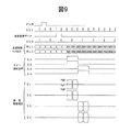
以上説明した本発明の走査ドライバ102の入出力信号のタイミングを図8、図9を用いて説明する。
【0036】
1ライン駆動モードの場合には、図8に示すようにFLM信号107はそのまま走査基準データとして用いられ、 CL1信号106はそのままCL3信号413として用いられる。走査基準データは走査ラインセレクタ406内をCL1信号106に従って順次シフトしていき、その結果、1ライン走査毎に1つのみが“走査”を示すライン選択信号S1〜Siが発生される。そして、ライン選択信号S1〜Siと、CL1信号106でラッチした直交関数W1(この場合は交流化M信号113となる)とがデコードされ、その結果に基づいて液晶駆動電圧Vy0〜Vy2が選択され出力される。
【0037】
また、2ライン駆動モードの場合は、図9に示すように、走査基準データとしてはFLM信号107信号を2走査期間分だけ遅延させたものが用いられ、走査ラインセレクタ406からは、走査ラインが2ラインずつ順次選択されるようにライン選択信号S1〜Siが発生される。そして、ライン選択信号S1〜Siと、CL1信号106でラッチされた直交関数W1,W2信号とがデコードされ、その結果に基づいて液晶駆動電圧Vy0〜Vy2が選択され出力される。
【0038】
なお、表示オフ制御信号DISPOFF信号108が”ロー”である場合、全てのライン選択信号S1〜Siが”非選択”の状態となるため、液晶走査駆動電圧Y1〜Yiは、すべてVy1電圧305となり、従って液晶パネル101の表示が停止される。
【0039】
次に本発明のデータドライバ103について図10〜図14を用いて説明する。図10は本発明のデータドライバ103の構成図であり、図11はデータドライバ103の動作説明図、図12はデータドライバ103の1出力あたりの駆動回路を示した図、図13,図14はデータドライバ103の入出力信号のタイミングチャ−トである。
【0040】
図10に示すように、データドライバ103は、ラッチアドレスセレクタ1001、クロック制御回路1002、入力データラッチ回路A1003、入力データラッチ回路B1004、ラインデータラッチ回路A1005、ラインデータラッチ回路B1010、演算回路1006、直交関数ラッチ回路1007、液晶電圧デコーダ1008、液晶電圧セレクタ1009で構成されている。
【0041】
ラッチアドレスセレクタ1001は2つの入力データラッチ回路のデータ取り込み用のタイミング信号A1〜Ajを生成する回路である。このラッチアドレスセレクタ1001はラインクロックCL1信号106でリセットされ、データラッチクロックCL2信号105のカウント値に従ってタイミング信号A1〜Ajを生成する。
【0042】
クロック制御部1002は、2入力データラッチ回路A1003およびB1004のどちらにデータを取り込ませるかを指示するプレーンセレクト信号PSを生成する回路である。この信号PSは、CL1信号106と、走査ドライバ102からの走査ライン転送クロックCL3信号412と、MODE信号410とに基づいて生成され、MODE信号410が”ロー”、すなわち1ライン駆動モードを示す場合には、入力データラッチ回路1003の選択を常に指示する。また、この信号PSは、MODE信号410が”ハイ”、すなわち2ライン駆動モードを示す場合には入力データラッチ回路A1003とB1004を1走査期間毎に交互に選択するように生成される。
【0043】
入力データラッチ回路A1003およびB1004は、データ電圧の出力チャンネル数(j個)だけのラッチ回路でそれぞれ構成され、クロック制御部1002からのPS信号により選択された場合に、表示データD7〜D0をラッチアドレスセレクタ1001からの信号Aに従って取り込む。
【0044】
ラインデータラッチ回路A1005およびB1010は、出力チャンネル数だけのラッチ回路でそれぞれ構成され、入力データラッチ回路A1003およびB1004が出力するデータを走査ライン転送クロックCL3信号412に従ってそれぞれラッチし、その結果を演算回路1006へ出力する。
【0045】
演算回路1006はデータ電圧の出力チャンネル数分の一致回路で構成され、ラインデータラッチ回路A1005およびB1010のラッチ結果と、走査ドライバ102の直交関数発生回路403(図4)にて生成された直交関数W1信号,W2信号とを入力する。データドライバ103の1出力に対応する演算回路は、図12に示すように、例えば2つの比較回路(EX−NOR)で構成される。比較器の一方がラインデータラッチ回路A1005の出力値と走査関数W1信号411とを比較し、他方がラインデータラッチ回路B1010の出力値とW2信号412の値を比較し、それらの比較結果が2ビットの一致数データDkとして出力される。
【0046】
この一致数データDkは、出力同期を図るた一致数データラッチ回路1007にてCL1信号106によりラッチされる。また、表示オフ制御DISPOFF信号108が”ロー”ならば、一致数データDkは強性的に十進表示で“1”となる。
【0047】
液晶電圧デコーダ1008および液晶電圧セレクタ1008は演算回路1006が出力する一致数データDkに従い、3レベルの液晶駆動用データ電圧の中から1レベルを選択して出力する。例えば図11に示すように、一致数が十進表示で“0”の時Vx0電圧309が選択され、一致数が“1”の時Vx1電圧310が選択され、一致数が”2”の時Vx2電圧311が選択される。
【0048】
以上で説明した本発明のデータドライバ103の入出力信号のタイミングについて図13、図14を用いて説明する。
【0049】
まず、1ライン駆動モードの場合、図13に示すように、表示データ104はラッチセレクト信号Aに従って入力データラッチ回路1003に順次取り込まれ、ラインラッチ回路1005では入力データラッチ回路1003から出力される表示データが、走査ライン選択CL3信号412(この場合CL3信号は1ラインクロックCL1と同じ信号)に従って1ライン期間保持される。そして、この保持した表示データと、CL1信号106でラッチされた走査関数W1(この場合交流化M信号113)とが比較演算され、その演算結果に対応する液晶駆動電圧Vy0〜Vy2が出力される。
【0050】
次に、2ライン駆動モードの場合、図14に示すように入力データラッチ回路A1003およびB1004が1ライン期間毎に選択され、データドライバの1回の出力当り2ライン分の表示データが取り込まれる。そしてラインラッチ回路1005では各入力データラッチ回路から出力される表示データが、走査ライン選択CL3信号412(この場合CL3信号は2ラインクロック)により2ライン期間保持され。そして、保持された表示データと、CL1信号106でラッチされた走査関数W1信号,W2信号とが比較演算され、その演算結果に対応する液晶駆動電圧Vy0〜Vy2が出力される。
【0051】
なお、上述したデータドライバ103は、液晶コントローラ109からの各種信号104〜108に従って走査ドライバ102と同期して動作を行う。また、走査ドライバ102およびデータドライバ103は常に、同一の直交関数W1,W2(または交流化M信号)を用いて液晶電圧のデコードを行う。
【0052】
以上説明したように、本実施例の液晶表示装置は、1ライン選択駆動と2ライン選択駆動をMODE信号410により切り替えることが可能である。したがって、データドライバの駆動電圧を5[V]以下にでき、従来の電圧平均化法に比べて低消費電力な駆動が可能となる。また、液晶パネルの走査ライン数Nが多くなっても2ライン選択駆動を行うことにより、走査ドライバの耐圧の問題を回避することが可能である。
【0053】
<第2実施例>
以下、本発明の第2の実施例を図15〜図20を用いて説明する。
【0054】
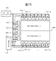
図15は、第2実施例に係る液晶表示装置の構成を示す図である。図において、1400は2画面で構成される640列×480行のカラー液晶パネル、1501は本発明の第2の走査ドライバ、1701は本発明の第2のデータドライバである。本実施例においては、走査ドライバ1501およびデータドライバ1701の各々に、直交関数を外部から入力可能とする機能と液晶ドライバのカスケード接続を可能とする機能とを設けることにより、液晶パネルを複数の走査ドライバと複数のデータドライバにより駆動できるようにしている。
【0055】
図16は本発明の第2の走査ドライバ1501の構成を示すブロック図、図17は本発明のクロック制御回路の動作説明図である。
【0056】
図16に示すように、走査ドライバ1501は、120チャンネル分の走査ライン電圧を出力可能であり、直交関数セレクタ1502、入力信号レベルシフタ1503、出力信号レベルシフタ1504、直交関数発生回路1505、直交関数ラッチ回路1506、クロック制御回路1507、走査ラインAセレクタ1508、走査ラインBセレクタ1509、液晶電圧レベルシフタ1510、液晶電圧デコーダ1511、液晶電圧セレクタ1512で構成されている。
【0057】
また、図中、410は1ライン駆動と2ライン駆動のいずれかのモードを指示するMODE信号、411〜412は2ビットの直交関数W1信号およびW2信号、413はライン転送クロックCL3信号であり、これらの信号は第1の実施例で説明したものと同じである。1513は、直交関数を内部で発生するのか、または外部から入力するのかを指示するマスタースレーブMS信号、1514〜1515は、走査ドライバ1501の液晶電圧出力が液晶パネルの1ライン目を含むか否か、すなわち当該走査ドライバ1501が各液晶パネルの先頭ドライバであるか否かを指示するLS信号である。図15においては、走査ドライバ1501−1および1501−4が先頭ドライバとなる。LS1信号1514は走査ラインAセレクタ1508の選択を指示する信号、LS2信号1515は走査ラインBセレクタ1509の選択を指示する信号、1516は液晶電圧出力のシフト方向を指示するSHL信号、1517〜1520は走査ラインセレクタの入出力データD1〜D4信号である。
【0058】
直交関数セレクタ1502は直交関数W1信号411およびW2信号412の入出力の切り替えを制御する回路であり、マスタースレーブMS信号1513が”ロー”(スレーブ)の時は、外部から入力される直交関数を入力信号レベルシフタ1503へ転送し、MS信号1513が”ハイ”(マスター)の時は、走査ドライバ1501内部で生成した直交関数を外部へ出力する。
【0059】
入力信号レベルシフタ1503は、第1実施例の走査ドライバで説明したものと同様に、VccとGNDレベルの入力信号群を、内部ロジック駆動用電圧であるVyCとVyLレベルにレベルシフトするための回路であり、出力信号レベルシフタ1504は、反対に内部ロジックで生成されるVyCとVyLレベルの信号群を、VccとGNDレベルの信号群にレベルシフトするための回路である。
【0060】
直交関数発生回路1505は、マスタースレーブMS信号1513が”ハイ”の時は、第1実施例と同様な動作で直交関数を発生する。すなわち、MODE信号410が”ロー”の場合には1ライン駆動モードとなり、直交関数W1信号411として交流化M信号119を入力し、これをそのまま次のブロックへ転送する。一方、MODE信号410が”ハイ”の場合には2ライン駆動モードとなり、ファーストラインマーカFLM信号107のカウント値とCL1信号106のカウント値に基づき、W1信号411、W2信号412、および走査ライン転送クロックCL3信号413を生成して出力する。また、マスタースレーブMS信号1513が”ロー”の時は、この回路は関数の発生を停止し、セレクタ1502を介して外部より入力した直交関数をそのまま転送する。なお、この直交関数発生回路1505内部で生成される直交関数は、第1実施例で説明したものと同様なものでよい。なお、直交関数W1,W2は液晶電圧レベルシフタ1510により高電圧に変換されるが、その前に出力同期を図るため、直交関数ラッチ回路1506にてCL1信号106によりラッチされる。
【0061】
クロック制御回路1507は、図17の動作説明図に示すように、LS1信号1514またはLS2信号1515が”ハイ”の場合、すなわち走査ドライバが先頭ドライバである場合、1ライン駆動モードではFLM信号107をそのまま走査ラインセレクタに転送し、2ライン駆動モードではFLM信号107を2走査期間分遅らせて転送する。また、LS1およびLS2信号が共に”ロー”の場合、すなわち当該走査ドライバが先頭ドライバでない場合、駆動モードに関わらず、前段のドライバから入力されるデータD信号をそのまま走査ラインセレクタに転送する。さらに、クロック制御回路1507は、走査ラインセレクタから出力されるデータD信号を外部に出力し、他の走査ドライバへ供給する。ここで、SHL信号1516が“ロー”の場合はD1信号1517とD3信号1519が入力信号、D2信号1518とD4信号1520が出力信号となり、SHL信号1516が”ハイ”の場合は反対にD1信号1517とD3信号1519が出力信号、D2信号1518とD4信号1520が入力信号となる。
【0062】
走査ラインAセレクタ1508は出力電圧Y1〜Y60にそれぞれ対応したシフト回路L1〜L60からなり、走査ラインBセレクタ1509は出力電圧Y61〜Y120にそれぞれ対応したシフト回路L60〜L120からなる。このうち、 シフト回路L1はデータD1の入出力を行い、シフト回路L60、L61、L120は、それぞれデータD2、D3、D4の入出力を行う。これらの走査ラインセレクタは共にクロック制御回路1507からのデータを、ラインクロックCL1信号412に従ってシフトさせ、ライン選択信号S1〜S60およびS61〜S120を出力する。また、各走査ラインセレクタは、クロック制御回路1507からの制御信号Cに従って、SHL信号1516が”ロー”(“0”)の場合はシフト回路L1からL60またはL61からL120の方向へデータをシフトさせ、SHL信号1516が“ハイ”(“1”)の場合は反対にシフト回路L61からL1またはL120からL61の方向へデータをシフトさせる。また、LS1およびLS2信号が共に“ロー”、すなわち走査ドライバが先頭ドライバでない場合、ドライバが120チャンネル出力として使用されるように、シフト回路L60とL61とが接続され、シフト回路L1およびL120がデータの入出力を行う。なお、表示オフ制御DISPOFF信号108が”ロー”の場合はこの回路のシフト動作は停止してリセット状態となる。
【0063】
図15においては、各走査ドライバ1501へ入力されるSHL信号1516はすべて“ハイ”となっており、各ドライバはY120からY1にかけてデータをシフトさせる。また、ドライバ1501−1および1501−3へのLS1信号は“0”、LS2信号は“1”、他のドライバ1501−2および1501−4へのLS1信号およびLS2信号は共に“0”となっている。
【0064】
液晶電圧レベルシフタ1510は第1実施例で説明したものと同様に、内部ロジック電源電圧レベルの信号を液晶駆動用の高電圧VyHとVyLレベルの電圧に昇圧する回路である。
【0065】
液晶電圧デコーダ1511および液晶電圧セレクタ1512は第1実施例の走査ドライバものと同様であり、ライン選択信号Sと直交関数W1およびW2の組合せに従い、3レベルの液晶駆動用走査電圧の中から1レベルを選択して出力する。例えば図7に示すように直交関数が”0”の時、選択信号が”選択”状態ならばVy0電圧304が選択され、選択信号が”非選択”状態ならばVy1電圧305が選択される。また、直交関数が”1”の時、選択信号が”選択”状態ならばVy2電圧306が選択され、選択信号が”非選択”状態ならばVy1電圧305が選択される。
【0066】
以上説明した第2の走査ドライバ1501ついて、その基本的な入出力信号タイミングは第1実施例の走査ドライバと同様であり、その詳細は第1実施例で説明した通りである。
【0067】
次に、第2実施例のデータドライバ1701について図18〜図19を用いて説明する。図18は本発明の第2のデータドライバ1701の構成を示すブロック図であり、図18はそのドライバにおける表示データ取り込み動作のタイミングチャートである。
【0068】
データドライバ1701は240チャンネルのデータ駆動電圧X1〜X240を出力するものであり、液晶パネル1400(図15)の上下にそれぞれ8個カスケード接続される。データドライバ1701は、図18に示すように、ラッチアドレスセレクタ1702、データ並び変え回路1703、クロック制御回路1704、入力データラッチ回路A1705、入力データラッチ回路B1706、ラインデータラッチ回路A1707、ラインデータラッチ回路B1720、演算回路1708、直交関数ラッチ回路1709、液晶電圧デコーダ1710、液晶電圧セレクタ1711で構成されている。また、図中、1712はデータドライバ1701の動作を制御するイネーブルE信号、1713はドライバのカスケード接続時に次段のE信号となるキャリーCAR信号である。例えば、図15において、データドライバ1701−1の出力するCAR信号はドライバ1701−2のイネーブルE信号となる。
【0069】
ラッチアドレスセレクタ1702は、入力データラッチ回路A1705およびB1706のデータ取り込み動作に用いられるタイミング信号を生成する回路であり、ラインクロックCL1信号106でリセットされ、データラッチクロックCL2信号105のカウント値に従ってタイミング信号を生成する。この回路はイネーブルE信号1712が”ロー”の時のみ動作し、最終段のデータ取り込み用タイミング信号はキャリーCAR信号1713として出力される。この動作を図19のタイミングチャートを用いて説明する。まず、液晶電圧出力が各パネルの1列目となるデータドライバ、すなわち図15のデータドライバ1701−1および1501−9に対して“ロー”のE信号1712が入力され、両ドライバが起動状態となる。起動されたドライバのラッチアドレスセレクタ1702は、データラッチクロックCL2信号105のカウント値に従って出力チャンネル数分(240個)のデータ取り込み信号を生成すると、自動的に停止状態(スタンバイ状態)となる。このときラインクロックCL1信号106の立下りで”ハイ”にセットされていたCAR信号1713が”ロー”となり、次段のデータドライバ1701−2および1701−10が起動する。このようにして順次各ドライバ1701に起動がかかり、1走査分の表示データが取り込まれる。なお、このラッチアドレスセレクタ1702は、SHL信号1416が“ロー”の場合はX1からX240の方向へ取り込み信号をシフトさせ、SHL信号1416が”ハイ”の場合は反対にX240からX1の方向へシフトさせる。図15の場合、データドライバ1701−1〜1701−8へ供給されるSHL信号1416は”ロー”であり、データドライバ1701−9〜1701−16へのSHL信号1416は”ハイ”である。
【0070】
データ並び変え回路1703は、SHL信号1416に従い表示データ104のビット並びを制御する回路であり、SHL信号1416が”ハイ”の場合には表示データ104のビット並びを反転させる。すなわち、図15のデータドライバ1701−9〜1701−16において、データの並び換えが行われる。
【0071】
クロック制御回路1704は第1実施例のデータドライバと同様に、2プレーンからなる入力データラッチ回路のうち、どちらのプレーンにデータを取り込ませるかを指示するプレーンセレクトPS信号を生成する回路である。このPS信号は、CL1信号106、走査ライン転送クロックCL3信号412およびMODE信号410から生成され、MODE信号410が”ロー”の場合は常に入力データラッチ回路A1705の選択を指示し、MODE信号410が”ハイ”の場合は入力データラッチ回路A1705と入力データラッチ回路B1706を1走査期間毎に交互に選択するように指示する。
【0072】
入力データラッチ回路A1705およびB1706は、出力チャンネル数分(240個)のラッチ回路でそれぞれ構成され、第1実施例と同様に、クロック制御回路1704からのPS信号により選択された入力データラッチ回路は、8ビットのパラレルデータをラッチアドレスセレクタ1702からの信号に従って取り込む。
【0073】
ラインデータラッチ回路A1707およびB1720は240出力分のラッチ回路でそれぞれ構成され、第1実施例と同様に、入力データラッチ回路が出力するデータを走査ライン転送クロックCL3信号412に従ってラッチし、その出力を演算回路1708へ伝える。
【0074】
演算回路1708は240出力分の演算回路で構成され、各演算回路は第1実施例と同様に、ラインデータラッチ回路A1707,B1720の出力値と走査関数W1信号411,W2信号412の値を一致回路により比較し、検出された一致数を2ビットの一致数データDkとして出力する。なお一致数Dkは出力同期を図るため、直交関数ラッチ回路1709にてCL1信号106によりラッチされる。また、表示オフ制御DISPOFF信号108が”ロー”ならば、一致数データは強性的に十進表示で”1”となる。
【0075】
液晶電圧デコーダ1710および液晶電圧セレクタ1711は、第1実施例と同様に、演算回路1708の出力する一致数データDkに従い、3レベルの液晶駆動用データ電圧の中から1レベルを選択して出力する。例えば図11に示すように一致が十進表示で”0”の時Vx0電圧309が選択され、一致が”1”の時Vx1電圧310が選択され、一致が”2”の時Vx2電圧311が選択されて出力される。
【0076】
以上説明したデータドライバ1701ついて、その基本的な入出力信号タイミングは第1実施例のデータドライバと同様であり、その詳細は第1実施例で説明した通りである。
【0077】
次に、以上説明した走査ドライバ1501およびデータドライバ1701を解像度(走査電極数)の異なる別の液晶パネルの駆動に用いた場合について説明する。
【0078】
図20はこの一例を示す液晶表示装置の構成図である。図に示すように、この液晶表示装置においては、2画面構成の800列×600行のカラー液晶パネル1800を駆動するために、その液晶パネル1800の上下に各10個のデータドライバ1701と、左側に5個の走査ドライバ1501を配置している。このうち走査ドライバ1501−7は、2つの液晶パネル1800aおよび1800bにまたがって配置され、60×2チャンネルで走査電圧を発生する。すなわち、走査ドライバ1501−7へは“ハイ”のLS1信号1514と、 “ロー”のLS2信号1515が供給され、走査ドライバ1501−7の走査電圧Y120〜Y61(図16参照)は液晶パネル1800aの走査用、走査電圧Y60〜Y1は液晶パネル1800bの走査用となっている。また、本例においては、走査ライン数と走査ドライバの出力電圧の関係(図2)から、走査ドライバ1501およびデータドライバ1701の各々には、2ライン駆動モードを示すMODE信号が供給されている。
【0079】
走査ドライバ1501−7以外の各走査ドライバ1501およびデータドライバ1701の動作は、図15を用いて説明したものと同様である。
【0080】
なお、以上では走査ドライバ1501を液晶パネルの左側に配置する場合についてのみ説明したが、走査ドライバ1501を右側に配置した構成の液晶表示装置も容易に実現できる。この場合には、走査ドライバ1501へ供給するSHL信号1516を“ロー”にして、走査が走査電圧Y1からY120にかけて行われるようにする。
【0081】
以上説明したように、第2実施例に係る液晶表示装置は、第1実施例のものと同様に、1ライン選択駆動と2ライン選択駆動をMODE信号410により切り替えることが可能である。したがって、データドライバの駆動電圧を5[V]以下にでき、従来の電圧平均化法に比べて低消費電力な駆動が可能となる。また、液晶パネルの走査ライン数Nが多くなっても2ライン選択駆動を行うことにより、走査ドライバの耐圧問題を回避することが可能である。
【0082】
また、本発明第2の液晶表示装置は、MS信号1413によって直交関数を外部から入力できることから、例えば内部で生成する直交関数よりも表示品質の良好な直交関数の組合せがある場合、これを入力することができ、拡張性をもたせることができる。さらに、SHL信号1416、D1〜D4信号1417〜1420、E信号1712、CAR信号1713によってドライバのカスケード接続ができることから、電極数の異なる液晶パネルにも対応可能であり、LS信号1414、1415により、120出力の走査ドライを60×2出力として使うことができ、解像度の異なる液晶パネルに対する適応性が向上する。
【0083】
なお、以上説明した本発明の液晶表示装置は、直交関数を発生する回路を内蔵し、データドライバには直交関数と表示データの一致数の演算を行う回路を内蔵している。これにより電圧平均化法による駆動を前提とした従来液晶コントローラとの互換性を保つことができ、実現コスト、消費電力の増大を防ぐことが可能となる。
【0084】
<第3実施例>
以下、本発明の第3の実施例を、図21〜図23を用いて説明する。
【0085】
本発明の第3の実施例は、走査ドライバに対し、アクティブマトリクス型液晶パネルの走査ドライバとしても使用できる機能を設けたものである。
【0086】
図21は本発明の第3の走査ドライバ2101の構成を示すブロック図、図22は走査ドライバ2101をアクティブマトリクス型液晶パネルの走査ドライバとして使用する場合の入出力信号のタイミングチャートであり、図23はこの場合の液晶表示装置の構成図である。
【0087】
本発明の第3の走査ドライバ2101は、120チャンネルのライン駆動電圧を発生するもので、図21に示すように、直交関数セレクタ2102、入力信号レベルシフタ2103、出力信号レベルシフタ2104、直交関数発生回路2105、直交関数ラッチ回路2106、クロック制御回路2107、走査ラインAセレクタ2108、走査ラインBセレクタ2109、液晶電圧レベルシフタ2110、液晶電圧デコーダ2111、液晶電圧セレクタ2112で構成されている。また、図中、410はMODE信号、411〜412は直交関数W1信号およびW2信号、413はライン転送クロックCL3信号、1513はマスタースレーブMS信号、1514〜1515はLS信号、1516は液晶電圧出力のシフト方向を指示するSHL信号、1517〜1520は走査ラインセレクタの入出力データD1〜D4信号であり、これらは本発明の第2実施例で説明したものと同じである。2113は、走査ドライバをアクティブマトリクス液晶パネル対応と単純マトリクス液晶パネル対応に切り替えるST信号である。
【0088】
走査ドライバ2101の各ブロックの動作は、液晶電圧デコーダ2111と液晶電圧セレクタ2112を除き、第2実施例の走査ドライバ1701と同じであるので、ここでは液晶電圧デコーダ2111および液晶電圧セレクタ2112の動作だけを説明する。液晶電圧デコーダ2111および液晶電圧セレクタ2112は、ライン選択信号と直交関数の組合せ、およびST信号2113に従い、3レベルの液晶駆動用走査電圧の中から1レベルを選択して出力する。
【0089】
例えばST信号2113が”ロー”の場合、単純マトリクス型液晶パネル対応となり、第2実施例と同様に、直交関数が”0”の時、選択信号が”選択”状態ならばVy0電圧304が選択され、選択信号が”非選択”状態ならばVy1電圧305が選択される。また、直交関数が”1”の時、選択信号が”選択”状態ならばVy2電圧306が選択され、選択信号が”非選択”状態ならばVy1電圧305が選択される。一方、ST信号2013が”ハイ”の場合、アクティブマトリクス型液晶パネル対応となり、直交関数の値にかかわらず、選択信号が”選択”状態ならばVy2電圧305が選択され、選択信号が”非選択”状態ならばVy0電圧303が選択される。なお、アクティブマトリクス型液晶パネル対応時のMODE信号410は”ロー”とし、直交関数W1、W2信号は使用しない。
【0090】
以上説明した本発明第3の走査ドライバ2101をアクティブマトリクス型液晶パネルの走査ドライバとして使用する場合の入出力信号タイミングは図22のようになる。図22に示すようにFLM信号107をCL3信号413(ここでは1ラインクロック)により取り込み、これをシフトして1ライン毎にライン選択信号を発生する。このライン選択信号に従い、液晶駆動用走査電圧Vy0とVy2中から1レベル選択して出力する。
【0091】
さらに、本発明の第3の走査ドライバ2101をアクティブマトリクス型液晶パネルの走査ドライバとして使用する場合の、液晶表示装置の構成図を図23に示す。図23において2301はスイッチング素子を有する例えばTFT型の液晶パネル、2302は[日立LCDドライバLSIデータブック第6版、P.799〜P.813(日立製作所半導体事業部発行)]に記載されたものに代表されるデータドライバ、2303はデータドライバ2302、走査ドライバ2101の動作タイミング信号を発生する液晶ドライバコントローラであり、第1の実施例と同様に、表示データ、データラッチクロック、ラインクロック、先頭ラインクロック、表示オフ制御信号等を出力する。2304は電源回路であり、上記データドライバ2302、コントローラ2303および走査ドライバ2101の駆動に必要な電圧群を生成する。
【0092】
以上説明した本発明の第3の走査ドライバ2101は、本発明の第1、第2の走査ドライバと同様に単純マトリクス型液晶パネルの走査ドライバとして使用できると共に、アクティブマトリクス型液晶パネルの走査ドライバとして使用することも可能となる。したがって、汎用性をさらに広げることが可能である。
【0093】
【発明の効果】
本発明のマトリクス表示装置は、複数ライン駆動方式に基づいたものであるため従来の電圧平均化駆動方式に比べて消費電力を小さくでき、また、走査ラインの選択数mを選択することができるため、走査ドライバおよびデータドライバの出力範囲内で走査ライン数Nの大きな種液晶パネルを駆動することができる。さらに、直交関数の発生手段および表示データと該直交関数との演算機能を内蔵しているため、走査ラインの選択数mにかかわらず従来の液晶コントローラをそのまま使用することができる。
【図面の簡単な説明】
【図1】本発明の第1実施例に係る液晶表示装置のブロック図である。
【図2】走査ライン数と液晶ドライバドの出力振幅値の関係を示す図である。
【図3】図1の電源回路115の構成を示すブロック図である。
【図4】図1の走査ドライバ102の構成を示すブロック図である。
【図5】図1の走査ドライバ内部で発生する直交関数を示す図である。
【図6】図5の直交関数の組合せを示す図である。
【図7】図1の走査ドライバの動作説明用のタイムチャートである。
【図8】図1の走査ドライバの動作説明用のタイムチャートである。
【図9】図1の走査ドライバの動作説明用のタイムチャートである。
【図10】図1のデータドライバ103のブロック構成図である。
【図11】図1のデータドライバの動作説明用のタイムチャートである。
【図12】図1のデータドライバの1出力当りの構成図である。
【図13】図1のデータドライバの動作説明用のタイムチャートである。
【図14】図1のデータドライバの動作説明用のタイムチャートである。
【図15】本発明の第2実施例に係る液晶表示装置の構成を示すブロック図である。
【図16】図15の走査ドライバ1501のブロック構成図である。
【図17】図16のクロック制御回路1507の動作説明用の図である。
【図18】図15のデータドライバ1701のブロック構成図である。
【図19】図15のデータドライバの動作説明用のタイムチャートである。
【図20】図15の液晶表示装置に別の液晶パネル適用した場合のブロック構成図である。
【図21】本発明の第3実施例に係る液晶表示装置の走査ドライバのブロック構成図である。
【図22】図21の走査ドライバの動作説明用のタイムチャートである。
【図23】本発明の第3実施例に係る液晶表示装置のブロック構成図である。
【符号の説明】
101…液晶パネル
102…データドライバ
103…走査ドライバ
104…表示データ
105…データラッチクロック
106…ラインクロック
107…先頭ラインクロック
108…表示オフ制御信号
112…交流化信号発生回路
116…電源回路
117…液晶駆動基準電圧
118…液晶駆動基準電圧
119…液晶駆動電圧制御用電圧
403…直交関数発生回路
410…駆動選択MODE信号
411…直交関数
412…直交関数
413…転送ラインクロック
1003…入力データラッチ回路A
1004…入力データラッチ回路B
1005…ラインデータラッチ回路
1508…走査ラインAセレクタ
1509…走査ラインBセレクタ
1513…マスタースレーブMS信号
1514…先頭ドライバ選択LS1信号
1515…先頭ドライバ選択LS2信号
1516…シフト方向選択SHL信号
1712…イネーブルE信号
1713…キャリーCAR信号
2113…駆動選択ST信号[0001]
[Industrial applications]
The present invention Matrix Especially simple for display devices Matrix The present invention relates to a liquid crystal display device that can be driven with low power consumption in a liquid crystal display device and a driving circuit thereof.
[0002]
[Prior art]
Simple Matrix As a driving method of a liquid crystal display device having a liquid crystal panel of a liquid crystal shape, published by the Industrial Research Council [Latest technology of liquid crystal, P.S. 106-P. 107] is widely adopted. In this method, a selective scanning voltage is sequentially applied to the scanning electrodes corresponding to the rows of the liquid crystal panel one by one for one scanning period, and when all the scanning electrodes are scanned in one frame period, the same operation is repeated again. A data voltage corresponding to the value of the display data is applied to the data electrodes corresponding to the columns of the liquid crystal panel around the non-selection scanning voltage level. Further, an alternating operation for inverting the polarity of the liquid crystal applied voltage at regular intervals is performed.
[0003]
On the other hand, simple Matrix As a driving method of a liquid crystal display device having a liquid crystal panel of a rectangular shape, there is a multiple line selection driving method described in JP-A-6-67628. In this system, a plurality of scanning electrodes corresponding to orthogonal functions (for example, Walsh functions) are sequentially applied to scanning electrodes corresponding to rows of a liquid crystal panel, and all the scanning electrodes are scanned in a period called one frame period. Then, the same operation is repeated again. The data electrodes corresponding to the columns of the liquid crystal panel are applied with data voltages corresponding to the number of coincidences with the value of the orthogonal function and the value of the display data in the selected and scanned line.
[0004]
Here, in the voltage averaging method, the voltage of the data driver and the voltage of the scan driver are level-shifted to the vicinity of the selection voltage of the scan driver during the AC operation, so that the output amplitudes are equal, and the value uses the number N of scan electrodes. hand,
[0005]
(Equation 1)
Given by On the other hand, the output amplitudes of the data driver and the scan driver in the multiple line selection drive method are calculated using the number m of selected lines and the number N of scan electrodes, respectively.
[0007]
(Equation 2)
[Equation 3]
Given by Here, Voff is an effective voltage value applied to the liquid crystal when the display is off, and usually takes a value of 2.0 to 2.5 [V]. In the multiple line selection driving method, when the value of the number m of lines is relatively small, for example, when m = 1, N = 240, and Voff = 2.2 [V], the amplitude of the data driver is about 3.3 [V] from
[0010]
[Problems to be solved by the invention]
In the multiple line selection driving method, when the number m of selected lines is a small value, the output amplitude of the data driver is small, but the amplitude of the scanning driver is large. Since the amplitude of the scan driver increases as the number N of scan electrodes increases, there is a problem that depending on the value of the number N of scan electrodes, the manufacture of the scan driver becomes difficult due to the problem of withstand voltage.
[0011]
On the other hand, when the number m of simultaneously selected scanning lines is a large value, it can be seen from
[0012]
Further, as the number m of simultaneously selected scanning lines increases, the scale of the circuit for calculating the number of coincidences between the orthogonal function and the display data increases, and there is a problem that the power consumption and the implementation cost of the circuit increase.
[0013]
Therefore, an object of the present invention is to provide a matrix panel display device capable of selecting the number m of simultaneously selected scanning lines according to the number N of scanning electrodes of a liquid crystal panel, and a driving circuit included therein.
[0014]
[Means for Solving the Problems]
In order to solve the above-described problem, it is necessary to first select the number m of selection lines that can clear the breakdown voltage of the scanning driver according to the number N of scanning electrodes. At the same time, it is important that the withstand voltage of the data driver be equal to or lower than the maximum output voltage of a process with low manufacturing cost.
[0015]
Thus, the relationship between the withstand voltage of the scan driver and the data driver with respect to the number of scanning lines N and the number of selected lines m was determined by setting the effective voltage value applied to the liquid crystal in the display off state to 2.3 V. This is shown in FIG. In FIG. 2, if the limit of the withstand voltage of the scanning driver is, for example, 50 V, it is possible to realize up to N = 245 rows when m = 1, up to N = 500 rows when m = 2, and more than N = 600 when m = 3. It can be seen that this is feasible. On the other hand, focusing on the withstand voltage of the data driver, for example, the condition of 5 V or less, which enables a logic process widely used at present, is the case where m = 2 or less. Therefore, for example, in order to perform display of 640 columns × 480 rows, which is one of the standard resolutions of a computer display, a liquid crystal panel of 640 columns × 240 rows with m = 1 or m = 2 has a two-screen configuration. What is necessary is just to drive. To display 800 columns × 600 rows, which is one of the standard resolutions, a liquid crystal panel of 800 columns × 300 rows may be driven in a two-screen configuration with m = 2.
[0016]
Focusing on the above points, the liquid crystal display device of the present invention provides a scanning driver that can select the number m of simultaneously selected scanning lines according to the resolution of the liquid crystal panel when, for example, m = 1 and m = 2. A data driver and a power supply circuit were provided. Further, the scan driver of the present invention includes a circuit for generating an orthogonal function, and the data driver includes a circuit for calculating the number of coincidences between the orthogonal function and the display data. This makes it possible to maintain compatibility with the conventional liquid crystal controller and prevent an increase in realization cost and power consumption. When the number m of simultaneously selected scanning lines is "1", the orthogonal function is not required, and the data driver outputs a voltage corresponding to the display data as in the voltage averaging method. For this reason, an alternating operation for preventing the deterioration of the liquid crystal is required. Therefore, a circuit for generating an alternating signal is provided.
[0017]
[Action]
Since the matrix display device of the present invention is based on the multi-line driving method, the power consumption can be reduced as compared with the conventional voltage averaging driving method, and the number m of scanning lines can be selected. Thus, a seed liquid crystal panel having a large number of scanning lines N can be driven within the output range of the scanning driver and the data driver. Further, since a function for generating an orthogonal function and a function for calculating display data and the orthogonal function are incorporated, a conventional liquid crystal controller can be used as it is regardless of the number m of scanning lines selected.
[0018]
【Example】
<First embodiment>
Hereinafter, a first embodiment of the present invention will be described with reference to FIGS. 1 and 3 to 14.
[0019]
FIG. 1 is a block diagram showing a configuration of a liquid crystal display device according to a first embodiment of the present invention.
[0020]
In FIG. 1, reference numeral 101 denotes a liquid crystal panel. In this embodiment, the liquid crystal panel 101 can display a matrix of i dots vertically and j dots horizontally. 102 is a scan driver of the present invention, and 103 is a data driver of the present invention.
[0021]
110 and 111 are control signal groups for controlling the operations of the
[0022]
Hereinafter, the configuration and operation of each block of the liquid crystal display device shown in FIG. 1 will be described with reference to FIGS.
[0023]
First, an example of the
[0024]
The scan driver
R1 = R4,
R2 = R3,
There is a relationship. Also, between the above voltages,
VyH = Vy2>Vy1> VyL = Vy0,
Vy2-Vy1 = Vy1-Vy0,
VxH>Vx2>Vx1>Vx0> VxL,
Vx2-Vx1 = Vx1-Vx0,
Vy1 = Vx1
There is a relationship. Note that the potential difference between the Vx2 voltage 311 and the Vx0 voltage 309 is given by
[0025]
Next, the configuration and operation of the
[0026]
As shown in FIG. 4, the
[0027]
The input signal level shifter 401 is a circuit for level shifting an input signal group of Vcc and GND levels to VyC and VyL levels, which are internal logic driving voltages, and the output signal level shifter 402 is generated by internal logic on the contrary. This is a circuit for level-shifting VyC and VyL level signal groups to Vcc and GND level signal groups. For these level shifts, a voltage group 115 supplied from a
[0028]
The orthogonal
[0029]
An example of an orthogonal function generated inside the orthogonal
[0030]
Further, the orthogonal
[0031]
The clock control circuit 405 transfers the FLM signal 107 as it is to the
[0032]
The
[0033]
The liquid crystal voltage level shifter 407 is a circuit that boosts a signal at the internal logic power supply voltage level to a high voltage VyH and VyL voltage for driving the liquid crystal. The voltage group 115 supplied from the
[0034]
The liquid crystal voltage decoder 408 and the liquid crystal voltage selector 409 select one of three levels of the liquid crystal driving scanning voltages Vy0 to Vy2 according to the combination of the line selection signals S1 to Si and the orthogonal function, and scan drive the result. Output as voltages Y1 to Yi. For example, as shown in FIG. 7, when the orthogonal function is “0”, if the selection signal is “selected” (scanning), the Vy0 voltage 304 is selected, and the selection signal is “unselected” (non-scanning). Then, the Vy1 voltage 305 is selected. When the orthogonal function is "1", the Vy2 voltage 306 is selected if the selection signal is in the "selected" state, and the Vy1 voltage 305 is selected if the selection signal is in the "non-selected" state.
[0035]
The input / output signal timings of the
[0036]
In the case of the one-line drive mode, as shown in FIG. 8, the
[0037]
In the case of the two-line drive mode, as shown in FIG. 9, as the scanning reference data, a signal obtained by delaying the FLM signal 107 by two scanning periods is used. Line selection signals S1 to Si are generated such that two lines are sequentially selected. Then, the line selection signals S1 to Si and the orthogonal function W1 and W2 signals latched by the CL1 signal 106 are decoded, and the liquid crystal driving voltages Vy0 to Vy2 are selected and output based on the decoding result.
[0038]
When the display-off control signal
[0039]
Next, the
[0040]
As shown in FIG. 10, the
[0041]
The latch address selector 1001 is a circuit that generates timing signals A1 to Aj for fetching data of two input data latch circuits. The latch address selector 1001 is reset by the line
[0042]
The
[0043]
The input data latch circuits A1003 and B1004 are each composed of latch circuits for the number of data voltage output channels (j), and latch the display data D7 to D0 when selected by the PS signal from the
[0044]
Line data latch circuits A1005 and B1010 are each constituted by latch circuits corresponding to the number of output channels, latch the data output from input data latch circuits A1003 and B1004 in accordance with scan line transfer
[0045]
The arithmetic circuit 1006 is constituted by matching circuits for the number of output channels of the data voltage, and the latch results of the line data latch circuits A1005 and B1010 and the orthogonal function generated by the orthogonal function generating circuit 403 (FIG. 4) of the
[0046]
The coincidence number data Dk is latched by the coincidence number
[0047]
The liquid
[0048]
The timing of the input / output signals of the
[0049]
First, in the case of the one-line drive mode, as shown in FIG. 13, the
[0050]
Next, in the case of the two-line drive mode, the input data latch circuits A1003 and B1004 are selected every one line period as shown in FIG. 14, and two lines of display data are taken in per output of the data driver. In the
[0051]
The
[0052]
As described above, the liquid crystal display device of this embodiment can switch between one-line selection driving and two-line selection driving by the
[0053]
<Second embodiment>
Hereinafter, a second embodiment of the present invention will be described with reference to FIGS.
[0054]
FIG. 15 is a diagram illustrating the configuration of the liquid crystal display device according to the second embodiment. In the figure, 1400 is a color liquid crystal panel of 640 columns × 480 rows composed of two screens, 1501 is a second scanning driver of the present invention, and 1701 is a second data driver of the present invention. In this embodiment, by providing each of the
[0055]
FIG. 16 is a block diagram showing the configuration of the
[0056]
As shown in FIG. 16, a
[0057]
In the figure,
[0058]
The
[0059]
The input
[0060]
When the master /
[0061]
As shown in the operation explanatory diagram of FIG. 17, when the
[0062]
The scanning
[0063]
In FIG. 15, the SHL signals 1516 input to each
[0064]
The liquid crystal
[0065]
The liquid
[0066]
The basic input / output signal timing of the
[0067]
Next, a data driver 1701 according to a second embodiment will be described with reference to FIGS. FIG. 18 is a block diagram showing a configuration of the second data driver 1701 of the present invention, and FIG. 18 is a timing chart of a display data fetching operation in the driver.
[0068]
The data driver 1701 outputs data drive voltages X1 to X240 of 240 channels, and eight data drivers 1701 are cascaded above and below the liquid crystal panel 1400 (FIG. 15). As shown in FIG. 18, the data driver 1701 includes a latch address selector 1702, a data rearrangement circuit 1703, a clock control circuit 1704, an input data
[0069]
The latch address selector 1702 is a circuit that generates a timing signal used for the data fetch operation of the input data latch circuits A1705 and B1706. The latch address selector 1702 is reset by the line
[0070]
The data rearrangement circuit 1703 controls the bit arrangement of the
[0071]
The clock control circuit 1704 is a circuit for generating a plane select PS signal for instructing which plane of the input data latch circuit composed of two planes to take in data, similarly to the data driver of the first embodiment. This PS signal is generated from the
[0072]
The input data latch circuits A1705 and B1706 are each composed of latch circuits for the number of output channels (240), and the input data latch circuits selected by the PS signal from the clock control circuit 1704 are the same as in the first embodiment. , 8-bit parallel data in accordance with a signal from the latch address selector 1702.
[0073]
Each of the line data latch circuits A1707 and B1720 is constituted by a latch circuit for 240 outputs, and latches data output from the input data latch circuit in accordance with the scan line transfer
[0074]
The arithmetic circuit 1708 is composed of arithmetic circuits for 240 outputs, and each arithmetic circuit matches the output values of the line data latch circuits A1707 and B1720 with the values of the scanning function W1 signal 411 and W2 signal 412, as in the first embodiment. The comparison is performed by the circuit, and the detected match number is output as 2-bit match number data Dk. The coincidence number Dk is latched by the orthogonal
[0075]
The liquid
[0076]
The basic timing of the input / output signal of the data driver 1701 described above is the same as that of the data driver of the first embodiment, and the details are as described in the first embodiment.
[0077]
Next, a case where the above-described
[0078]
FIG. 20 is a configuration diagram of a liquid crystal display device showing this example. As shown in the figure, in this liquid crystal display device, in order to drive a 800-color × 600-row color
[0079]
The operation of each
[0080]
Although only the case where the
[0081]
As described above, the liquid crystal display device according to the second embodiment can switch between one-line selection driving and two-line selection driving by the MODE signal 410 as in the first embodiment. Therefore, the driving voltage of the data driver can be reduced to 5 [V] or less, and driving with lower power consumption than the conventional voltage averaging method can be performed. Further, even if the number N of scanning lines of the liquid crystal panel increases, by performing the two-line selection driving, it is possible to avoid the withstand voltage problem of the scanning driver.
[0082]
Further, since the orthogonal function can be externally input by the MS signal 1413 according to the second liquid crystal display device of the present invention, for example, when there is a combination of orthogonal functions having better display quality than the orthogonal function generated internally, this is input. And expandability can be provided. Furthermore, since the cascade connection of the driver can be performed by the SHL signal 1416, the D1 to D4 signals 1417 to 1420, the
[0083]
The liquid crystal display device of the present invention described above has a built-in circuit for generating an orthogonal function, and the data driver has a circuit for calculating the number of coincidences between the orthogonal function and the display data. As a result, it is possible to maintain compatibility with a conventional liquid crystal controller on the premise of driving by the voltage averaging method, and it is possible to prevent an increase in realization cost and power consumption.
[0084]
<Third embodiment>
Hereinafter, a third embodiment of the present invention will be described with reference to FIGS.
[0085]
In the third embodiment of the present invention, a function that can be used as a scan driver of an active matrix type liquid crystal panel is provided to the scan driver.
[0086]
FIG. 21 is a block diagram showing a configuration of the
[0087]
The
[0088]
The operation of each block of the
[0089]
For example, when the
[0090]
FIG. 22 shows input / output signal timings when the above-described
[0091]
Further, FIG. 23 shows a configuration diagram of a liquid crystal display device when the
[0092]
The
[0093]
【The invention's effect】
Since the matrix display device of the present invention is based on the multi-line driving method, the power consumption can be reduced as compared with the conventional voltage averaging driving method, and the number m of scanning lines can be selected. Thus, a seed liquid crystal panel having a large number of scanning lines N can be driven within the output range of the scanning driver and the data driver. Further, since a function for generating an orthogonal function and a function for calculating display data and the orthogonal function are incorporated, a conventional liquid crystal controller can be used as it is regardless of the number m of scanning lines selected.
[Brief description of the drawings]
FIG. 1 is a block diagram of a liquid crystal display device according to a first embodiment of the present invention.
FIG. 2 is a diagram showing a relationship between the number of scanning lines and an output amplitude value of a liquid crystal driver.
FIG. 3 is a block diagram showing a configuration of a power supply circuit 115 of FIG.
FIG. 4 is a block diagram showing a configuration of a
FIG. 5 is a diagram showing an orthogonal function generated inside the scan driver of FIG. 1;
FIG. 6 is a diagram showing combinations of orthogonal functions in FIG. 5;
FIG. 7 is a time chart for explaining the operation of the scanning driver of FIG. 1;
FIG. 8 is a time chart for explaining the operation of the scanning driver of FIG. 1;
FIG. 9 is a time chart for explaining the operation of the scanning driver of FIG. 1;
FIG. 10 is a block diagram of the
FIG. 11 is a time chart for explaining the operation of the data driver of FIG. 1;
FIG. 12 is a configuration diagram per output of the data driver of FIG. 1;
FIG. 13 is a time chart for explaining the operation of the data driver in FIG. 1;
FIG. 14 is a time chart for explaining the operation of the data driver in FIG. 1;
FIG. 15 is a block diagram illustrating a configuration of a liquid crystal display device according to a second embodiment of the present invention.
FIG. 16 is a block diagram of a
17 is a diagram for explaining an operation of the
FIG. 18 is a block diagram of the data driver 1701 of FIG.
FIG. 19 is a time chart for explaining the operation of the data driver in FIG. 15;
20 is a block diagram showing a case where another liquid crystal panel is applied to the liquid crystal display device of FIG.
FIG. 21 is a block diagram of a scan driver of a liquid crystal display according to a third embodiment of the present invention.
FIG. 22 is a time chart for explaining the operation of the scanning driver in FIG. 21;
FIG. 23 is a block diagram of a liquid crystal display device according to a third embodiment of the present invention.
[Explanation of symbols]
101 ... Liquid crystal panel
102 Data driver
103 ... Scan driver
104 ... display data
105: Data latch clock
106 ... Line clock
107: First line clock
108: display off control signal
112 ... AC signal generation circuit
116 ... Power supply circuit
117 ... Liquid crystal drive reference voltage
118 ... Liquid crystal drive reference voltage
119: liquid crystal drive voltage control voltage
403 ... Orthogonal function generation circuit
410: drive selection MODE signal
411: orthogonal function
412: orthogonal function
413: transfer line clock
1003: input data latch circuit A
1004... Input data latch circuit B
1005 ... Line data latch circuit
1508 Scanning line A selector
1509 scanning line B selector
1513: Master slave MS signal
1514: LS1 signal for head driver selection
1515: Leading driver selection LS2 signal
1516: Shift direction selection SHL signal
1712: Enable E signal
1713: Carry CAR signal
2113 ... Drive selection ST signal
Claims (10)
前記同期信号に同期してm(mは3以上の自然数)個の直交関数信号を生成する直交関数発生手段と、
前記モード選択信号が第1のモードを示す場合には前記同期信号に同期して駆動対象の走査電極を1ずつ順次選択し、第2のモードを示す場合には駆動対象の走査電極をm個ずつ順次選択する走査電極選択手段と、
前記モード選択信号が第1のモードを示す場合には、前記走査電極選択手段により順次選択される走査電極に前記交流化信号にて定まる、前記複数の駆動電圧信号のいずれかを供給し、第2のモードを示す場合には、前記走査電極選択手段により順次選択されるm個の走査電極のそれぞれに、前記m個の直交関数信号のうちの予め対応付けられた直交関数信号にて定まる、前記複数の駆動電圧信号のいずれかを供給する電圧信号選択手段と
を有することを特徴とする走査電圧駆動回路。A scan voltage driver circuit for controlling a matrix panel having a plurality of scan electrodes and a plurality of data electrodes via the plurality of scan electrodes, wherein the scan voltage driver circuit inverts a synchronization signal and a value at a predetermined cycle. And a plurality of drive voltage signals having different levels from each other, and a mode selection signal indicating one of the first mode and the second mode.
Orthogonal function generating means for generating m (m is a natural number of 3 or more) orthogonal function signals in synchronization with the synchronization signal;
When the mode selection signal indicates the first mode, the scan electrodes to be driven are sequentially selected one by one in synchronization with the synchronization signal, and when the mode selection signal indicates the second mode, m scan electrodes to be driven are selected. Scanning electrode selecting means for sequentially selecting each one;
When the mode selection signal indicates the first mode, any one of the plurality of drive voltage signals determined by the alternating signal is supplied to scan electrodes sequentially selected by the scan electrode selection means, In the case of indicating the second mode, each of the m scan electrodes sequentially selected by the scan electrode selecting means is determined by an orthogonal function signal associated with the m orthogonal function signals in advance. A voltage signal selection unit for supplying any one of the plurality of drive voltage signals.
前記同期信号に同期して2つの直交関数信号を生成する直交関数発生手段と、前記モード選択信号が第1のモードを示す場合には前記同期信号に同期して駆動対象の走査電極を1ずつ順次選択し、第2のモードを示す場合には駆動対象の走査電極を2ずつ順次選択する走査電極選択手段と、
前記モード選択信号が第1のモードを示す場合には、前記走査電極選択手段により順次選択される走査電極に前記交流化信号にて定まる、前記複数の駆動電圧信号のいずれかを供給し、第2のモードを示す場合には、前記走査電極選択手段により順次選択される2つの走査電極のそれぞれに、前記2つの直交関数信号のうちの予め対応付けられた直交関数信号にて定まる、前記複数の駆動電圧信号のいずれかを供給する電圧信号選択手段と
を有することを特徴とする走査電圧駆動回路。A scan voltage driver circuit for controlling a matrix panel having a plurality of scan electrodes and a plurality of data electrodes via the plurality of scan electrodes, wherein the scan voltage driver circuit inverts a synchronization signal and a value at a predetermined cycle. And a plurality of drive voltage signals having different levels from each other, and a mode selection signal indicating one of the first mode and the second mode.
Orthogonal function generating means for generating two orthogonal function signals in synchronization with the synchronization signal; and, when the mode selection signal indicates the first mode, scanning electrodes to be driven one by one in synchronization with the synchronization signal. Scanning electrode selecting means for sequentially selecting, and when the second mode is indicated, sequentially selecting two scan electrodes to be driven sequentially;
When the mode selection signal indicates the first mode, any one of the plurality of drive voltage signals determined by the alternating signal is supplied to scan electrodes sequentially selected by the scan electrode selection means, In the case of indicating the second mode, each of the two scan electrodes sequentially selected by the scan electrode selecting means is determined by the orthogonal function signal associated with the two orthogonal function signals in advance. And a voltage signal selecting means for supplying one of the drive voltage signals.
前記複数の駆動電圧信号は、前記走査電極の非選択時に当該走査電極に印可される第1の電圧信号と、当該非選択電圧信号の電圧に対してプラス側の電圧の信号であって前記走査電極の選択時に当該走査電極に印可される第2の電圧信号と、当該非選択電圧信号の電圧に対してマイナス側の電圧の信号であって前記走査電極の選択時に当該走査電極に印可される第3の電圧信号とからなることを特徴とする走査電圧駆動回路。The scanning voltage driving circuit according to claim 2, wherein
The plurality of drive voltage signals are a first voltage signal applied to the scan electrode when the scan electrode is not selected, and a signal of a voltage on the positive side with respect to the voltage of the non-selection voltage signal. A second voltage signal applied to the scan electrode when the electrode is selected, and a signal of a voltage on the negative side with respect to the voltage of the non-selection voltage signal, which is applied to the scan electrode when the scan electrode is selected. A scanning voltage driving circuit, comprising: a third voltage signal.
前記走査電極選択手段は、前記複数の走査電極を少なくとも2つの選択対象に分割し、当該選択対象毎に走査電極の選択を行うことを特徴とする走査電圧駆動回路。The scanning voltage driving circuit according to claim 2, wherein
A scanning voltage driving circuit, wherein the scanning electrode selecting means divides the plurality of scanning electrodes into at least two selection targets, and selects a scanning electrode for each of the selection targets.
前記直交関数発生手段が生成する2つの直交関数信号と、外部から入力される2つの直交関数信号と、前記交流化信号との内のいずれかを選択し、選択した信号を前記電圧信号選択手段へ与える手段を有することを特徴とする走査電圧駆動回路。The scanning voltage driving circuit according to claim 2, wherein
The orthogonal signal generator selects one of the two orthogonal function signals generated by the orthogonal function generator, the two orthogonal function signals input from the outside, and the AC signal, and selects the selected signal from the voltage signal selector. A scanning voltage driving circuit, comprising: a scanning voltage driving circuit.
直交する走査電極とデータ電極の交点にスイッチ素子を有し当該走査電極には当該走査電極の選択を示すスイッチオン電圧と非選択を示すスイッチオフ電圧のいずれかが印加されるマトリクスパネルの駆動時に、
前記駆動電圧選択手段は、スイッチオン電圧として前記第2の電圧を選択し、スイッチオフ電圧として前記第3の電圧を選択することを特徴とする走査電圧駆動回路。The scanning voltage driving circuit according to claim 2, wherein
At the time of driving a matrix panel, a switch element is provided at the intersection of the orthogonal scan electrode and data electrode, and either a switch-on voltage indicating selection of the scan electrode or a switch-off voltage indicating non-selection is applied to the scan electrode. ,
The scanning voltage drive circuit, wherein the drive voltage selection means selects the second voltage as a switch-on voltage, and selects the third voltage as a switch-off voltage.
前記同期信号に同期して特定の走査電極に対応した表示データを取り込む第1のデータ保持手段と、
前記モード選択信号が第2のモードを示す場合に、前記特定の走査電極とは異なる(m−1)個の走査電極に対応した表示データを取り込む第2のデータ保持手段と、
前記モード選択信号が第1のモードを示す場合には、前記第1のデータ保持手段の保持しているデータの値と交流化信号との間で所定の演算を行い、第2のモードを示す場合には、前記第1および第2のデータ保持手段の保持しているデータの値と前記m個の直交関数信号の間で所定の演算を行う演算回路と、
前記複数のデータ電極のそれぞれに、当該演算結果に応じて定まる、前記複数の駆動電圧信号の内のいずれかを供給する電圧信号選択手段と
を有することを特徴とするデータ電圧駆動回路。A data voltage drive circuit for controlling a matrix panel having a plurality of scan electrodes and a plurality of data electrodes via the plurality of data electrodes, wherein the data voltage drive circuit includes a synchronization signal, m (m is 3 or more) (Natural number) orthogonal function signals, an alternating signal whose value is inverted at a predetermined cycle, a mode selection signal indicating one of the first mode and the second mode, and display data. Having a plurality of driving voltage signals,
First data holding means for capturing display data corresponding to a specific scan electrode in synchronization with the synchronization signal;
A second data holding unit that, when the mode selection signal indicates the second mode, captures display data corresponding to (m−1) scan electrodes different from the specific scan electrode;
When the mode selection signal indicates the first mode, a predetermined operation is performed between the value of the data held by the first data holding means and the alternating signal to indicate the second mode. In this case, an arithmetic circuit that performs a predetermined operation between the data values held by the first and second data holding means and the m orthogonal function signals;
A data voltage driving circuit, comprising: a voltage signal selecting unit that supplies one of the plurality of driving voltage signals to each of the plurality of data electrodes, which is determined according to a result of the calculation.
前記同期信号に同期して特定の走査電極に対応した表示データを取り込む第1のデータ保持手段と、
前記モード選択信号が第2のモードを示す場合に、前記特定の走査電極とは異なる走査電極に対応した表示データを取り込む第2のデータ保持手段と、
前記モード選択信号が第1のモードを示す場合には、前記第1のデータ保持手段の保持しているデータの値と交流化信号の間で所定の演算を行い、第2のモードを示す場合には、前記第1および第2のデータ保持手段の保持しているデータの値と前記2つの直交関数信号の間で所定の演算を行う演算回路と、
前記モード選択信号が第1のモードを示す場合には、前記複数のデータ電極のそれぞれに、当該演算結果に応じて定まる、前記複数の駆動電圧信号のうちの所定の2つの駆動電圧信号のいずれかを供給し、第2のモードを示す場合には、前記複数のデータ電極のそれぞれに、当該演算結果に応じて定まる、前記複数の駆動電圧信号の内の所定の3つの駆動電圧信号のいずれかを供給する電圧信号選択手段と
を有することを特徴とするデータ電圧駆動回路。A data voltage drive circuit that controls a matrix panel having a plurality of scan electrodes and a plurality of data electrodes via the plurality of data electrodes, wherein the data voltage drive circuit includes a synchronization signal, two orthogonal function signals, An alternating signal whose value is inverted at a predetermined cycle, a mode selection signal indicating one of the first mode and the second mode, display data, and a plurality of drive voltage signals having different levels are input. Things,
First data holding means for capturing display data corresponding to a specific scan electrode in synchronization with the synchronization signal;
When the mode selection signal indicates a second mode, a second data holding unit that captures display data corresponding to a scan electrode different from the specific scan electrode;
When the mode selection signal indicates the first mode, a predetermined operation is performed between the value of the data held by the first data holding means and the AC signal, and the second mode is indicated. An arithmetic circuit for performing a predetermined operation between the value of the data held by the first and second data holding means and the two orthogonal function signals;
When the mode selection signal indicates the first mode, one of the predetermined two drive voltage signals of the plurality of drive voltage signals, which is determined according to the calculation result, is applied to each of the plurality of data electrodes. Is supplied to indicate the second mode, any one of the predetermined three drive voltage signals among the plurality of drive voltage signals, which is determined according to the calculation result, is applied to each of the plurality of data electrodes. And a voltage signal selection means for supplying the data voltage.
請求項8記載のデータ電圧駆動回路と、
所定の周期で値が反転する交流化信号を生成する交流化信号発生回路と、
前記走査電圧駆動回路とデータ電圧駆動回路と交流化信号生成手段とを駆動するための電圧信号を発生する電源手段と
からなるマトリクスパネル制御装置。A scanning voltage driving circuit according to claim 2,
A data voltage driving circuit according to claim 8,
An alternating signal generating circuit that generates an alternating signal whose value is inverted at a predetermined cycle;
A matrix panel control device comprising: a power supply unit that generates a voltage signal for driving the scanning voltage driving circuit, the data voltage driving circuit, and the AC signal generating unit.
請求項2記載の走査電圧駆動回路と、
請求項8記載のデータ電圧駆動回路と、
所定の周期で値が反転する交流化信号を生成する交流化信号発生回路と、
前記マトリクスパネルと走査電圧駆動回路とデータ電圧駆動回路と交流化信号生成手段とを駆動するための電圧信号を発生する電源手段と
からなるマトリクスパネル表示装置。A matrix panel having a plurality of scan electrodes and a plurality of data electrodes,
A scanning voltage driving circuit according to claim 2,
A data voltage driving circuit according to claim 8,
An alternating signal generating circuit that generates an alternating signal whose value is inverted at a predetermined cycle;
A matrix panel display device comprising: a power supply unit for generating a voltage signal for driving the matrix panel, a scanning voltage driving circuit, a data voltage driving circuit, and an alternating signal generating unit.
Priority Applications (1)
| Application Number | Priority Date | Filing Date | Title |
|---|---|---|---|
| JP10663995A JP3544580B2 (en) | 1995-04-28 | 1995-04-28 | Matrix panel display device, matrix panel control device, scanning voltage driving circuit and data voltage driving circuit thereof |
Applications Claiming Priority (1)
| Application Number | Priority Date | Filing Date | Title |
|---|---|---|---|
| JP10663995A JP3544580B2 (en) | 1995-04-28 | 1995-04-28 | Matrix panel display device, matrix panel control device, scanning voltage driving circuit and data voltage driving circuit thereof |
Publications (2)
| Publication Number | Publication Date |
|---|---|
| JPH08304760A JPH08304760A (en) | 1996-11-22 |
| JP3544580B2 true JP3544580B2 (en) | 2004-07-21 |
Family
ID=14438695
Family Applications (1)
| Application Number | Title | Priority Date | Filing Date |
|---|---|---|---|
| JP10663995A Expired - Fee Related JP3544580B2 (en) | 1995-04-28 | 1995-04-28 | Matrix panel display device, matrix panel control device, scanning voltage driving circuit and data voltage driving circuit thereof |
Country Status (1)
| Country | Link |
|---|---|
| JP (1) | JP3544580B2 (en) |
Families Citing this family (3)
| Publication number | Priority date | Publication date | Assignee | Title |
|---|---|---|---|---|
| GB9827964D0 (en) * | 1998-12-19 | 1999-02-10 | Secr Defence | Active backplane circuitry |
| JP4290627B2 (en) | 2004-10-04 | 2009-07-08 | シャープ株式会社 | Display element driving apparatus, display device including the display element driving apparatus, and display element driving method |
| JP4907908B2 (en) * | 2005-06-29 | 2012-04-04 | ルネサスエレクトロニクス株式会社 | Driving circuit and display device |
-
1995
- 1995-04-28 JP JP10663995A patent/JP3544580B2/en not_active Expired - Fee Related
Also Published As
| Publication number | Publication date |
|---|---|
| JPH08304760A (en) | 1996-11-22 |
Similar Documents
| Publication | Publication Date | Title |
|---|---|---|
| JP3774248B2 (en) | Liquid crystal display | |
| JP5649858B2 (en) | Liquid crystal display device, liquid crystal display panel drive device, and liquid crystal display panel | |
| US20040239602A1 (en) | Method and apparatus for driving liquid crystal display device | |
| JP2006524365A (en) | Display system with frame buffer and power saving sequence | |
| US20060028426A1 (en) | LCD apparatus for improved inversion drive | |
| JPH08179731A (en) | Data driver, scan driver, liquid crystal display device and driving method thereof | |
| US8054276B2 (en) | Display apparatus and display drive circuit | |
| JP4175058B2 (en) | Display drive circuit and display device | |
| WO2009101877A1 (en) | Display apparatus and method for driving the same | |
| JP4313281B2 (en) | Multiple screen scanning method and apparatus | |
| CN109658899B (en) | Voltage switching circuit, gamma voltage generating circuit and liquid crystal display device | |
| JP3544580B2 (en) | Matrix panel display device, matrix panel control device, scanning voltage driving circuit and data voltage driving circuit thereof | |
| JP3669514B2 (en) | Driving circuit for liquid crystal display device | |
| JPH0876091A (en) | Liquid crystal panel driving method and apparatus | |
| KR20140025169A (en) | Driver circuit and display device having them | |
| JPH09160526A (en) | Drive circuit of matrix type display panel and display device using the drive circuit | |
| CN101162335A (en) | Gate driver, electro-optical device, electronic instrument, and drive method | |
| JPH06175610A (en) | X-driving circuit | |
| JPH07225567A (en) | Gradation driving circuit for active matrix liquid crystal display device and liquid crystal display device therefor | |
| JPH06118904A (en) | LCD drive circuit | |
| JPH06167947A (en) | Driving method, driving circuit and display device for liquid crystal element or the like | |
| CN114974162B (en) | Circuit for providing capacitor charging parameters, TCON and display device | |
| JPH07114001A (en) | Liquid crystal display | |
| JP3556023B2 (en) | Liquid crystal display | |
| JP2011170376A (en) | Liquid crystal display driving device, liquid crystal display system, and semiconductor integrated circuit device for driving liquid crystal |
Legal Events
| Date | Code | Title | Description |
|---|---|---|---|
| A977 | Report on retrieval |
Free format text: JAPANESE INTERMEDIATE CODE: A971007 Effective date: 20040308 |
|
| TRDD | Decision of grant or rejection written | ||
| A01 | Written decision to grant a patent or to grant a registration (utility model) |
Free format text: JAPANESE INTERMEDIATE CODE: A01 Effective date: 20040330 |
|
| A61 | First payment of annual fees (during grant procedure) |
Free format text: JAPANESE INTERMEDIATE CODE: A61 Effective date: 20040405 |
|
| R150 | Certificate of patent or registration of utility model |
Free format text: JAPANESE INTERMEDIATE CODE: R150 |
|
| FPAY | Renewal fee payment (event date is renewal date of database) |
Free format text: PAYMENT UNTIL: 20090416 Year of fee payment: 5 |
|
| FPAY | Renewal fee payment (event date is renewal date of database) |
Free format text: PAYMENT UNTIL: 20090416 Year of fee payment: 5 |
|
| FPAY | Renewal fee payment (event date is renewal date of database) |
Free format text: PAYMENT UNTIL: 20100416 Year of fee payment: 6 |
|
| LAPS | Cancellation because of no payment of annual fees |