CN1193488C - Buffer circuit, and power conversion device using same - Google Patents
Buffer circuit, and power conversion device using same Download PDFInfo
- Publication number
- CN1193488C CN1193488C CNB011385669A CN01138566A CN1193488C CN 1193488 C CN1193488 C CN 1193488C CN B011385669 A CNB011385669 A CN B011385669A CN 01138566 A CN01138566 A CN 01138566A CN 1193488 C CN1193488 C CN 1193488C
- Authority
- CN
- China
- Prior art keywords
- diode
- series circuit
- capacitor
- series
- coil
- Prior art date
- Legal status (The legal status is an assumption and is not a legal conclusion. Google has not performed a legal analysis and makes no representation as to the accuracy of the status listed.)
- Expired - Fee Related
Links
Images





Classifications
-
- H—ELECTRICITY
- H02—GENERATION; CONVERSION OR DISTRIBUTION OF ELECTRIC POWER
- H02M—APPARATUS FOR CONVERSION BETWEEN AC AND AC, BETWEEN AC AND DC, OR BETWEEN DC AND DC, AND FOR USE WITH MAINS OR SIMILAR POWER SUPPLY SYSTEMS; CONVERSION OF DC OR AC INPUT POWER INTO SURGE OUTPUT POWER; CONTROL OR REGULATION THEREOF
- H02M3/00—Conversion of DC power input into DC power output
- H02M3/22—Conversion of DC power input into DC power output with intermediate conversion into AC
- H02M3/24—Conversion of DC power input into DC power output with intermediate conversion into AC by static converters
- H02M3/28—Conversion of DC power input into DC power output with intermediate conversion into AC by static converters using discharge tubes with control electrode or semiconductor devices with control electrode to produce the intermediate AC
-
- H—ELECTRICITY
- H02—GENERATION; CONVERSION OR DISTRIBUTION OF ELECTRIC POWER
- H02M—APPARATUS FOR CONVERSION BETWEEN AC AND AC, BETWEEN AC AND DC, OR BETWEEN DC AND DC, AND FOR USE WITH MAINS OR SIMILAR POWER SUPPLY SYSTEMS; CONVERSION OF DC OR AC INPUT POWER INTO SURGE OUTPUT POWER; CONTROL OR REGULATION THEREOF
- H02M1/00—Details of apparatus for conversion
- H02M1/32—Means for protecting converters other than automatic disconnection
- H02M1/34—Snubber circuits
-
- H—ELECTRICITY
- H02—GENERATION; CONVERSION OR DISTRIBUTION OF ELECTRIC POWER
- H02M—APPARATUS FOR CONVERSION BETWEEN AC AND AC, BETWEEN AC AND DC, OR BETWEEN DC AND DC, AND FOR USE WITH MAINS OR SIMILAR POWER SUPPLY SYSTEMS; CONVERSION OF DC OR AC INPUT POWER INTO SURGE OUTPUT POWER; CONTROL OR REGULATION THEREOF
- H02M3/00—Conversion of DC power input into DC power output
- H02M3/22—Conversion of DC power input into DC power output with intermediate conversion into AC
- H02M3/24—Conversion of DC power input into DC power output with intermediate conversion into AC by static converters
- H02M3/28—Conversion of DC power input into DC power output with intermediate conversion into AC by static converters using discharge tubes with control electrode or semiconductor devices with control electrode to produce the intermediate AC
- H02M3/325—Conversion of DC power input into DC power output with intermediate conversion into AC by static converters using discharge tubes with control electrode or semiconductor devices with control electrode to produce the intermediate AC using devices of a triode or a transistor type requiring continuous application of a control signal
- H02M3/335—Conversion of DC power input into DC power output with intermediate conversion into AC by static converters using discharge tubes with control electrode or semiconductor devices with control electrode to produce the intermediate AC using devices of a triode or a transistor type requiring continuous application of a control signal using semiconductor devices only
- H02M3/33538—Conversion of DC power input into DC power output with intermediate conversion into AC by static converters using discharge tubes with control electrode or semiconductor devices with control electrode to produce the intermediate AC using devices of a triode or a transistor type requiring continuous application of a control signal using semiconductor devices only of the forward type
-
- H—ELECTRICITY
- H02—GENERATION; CONVERSION OR DISTRIBUTION OF ELECTRIC POWER
- H02M—APPARATUS FOR CONVERSION BETWEEN AC AND AC, BETWEEN AC AND DC, OR BETWEEN DC AND DC, AND FOR USE WITH MAINS OR SIMILAR POWER SUPPLY SYSTEMS; CONVERSION OF DC OR AC INPUT POWER INTO SURGE OUTPUT POWER; CONTROL OR REGULATION THEREOF
- H02M1/00—Details of apparatus for conversion
- H02M1/32—Means for protecting converters other than automatic disconnection
- H02M1/34—Snubber circuits
- H02M1/346—Passive non-dissipative snubbers
-
- Y—GENERAL TAGGING OF NEW TECHNOLOGICAL DEVELOPMENTS; GENERAL TAGGING OF CROSS-SECTIONAL TECHNOLOGIES SPANNING OVER SEVERAL SECTIONS OF THE IPC; TECHNICAL SUBJECTS COVERED BY FORMER USPC CROSS-REFERENCE ART COLLECTIONS [XRACs] AND DIGESTS
- Y02—TECHNOLOGIES OR APPLICATIONS FOR MITIGATION OR ADAPTATION AGAINST CLIMATE CHANGE
- Y02B—CLIMATE CHANGE MITIGATION TECHNOLOGIES RELATED TO BUILDINGS, e.g. HOUSING, HOUSE APPLIANCES OR RELATED END-USER APPLICATIONS
- Y02B70/00—Technologies for an efficient end-user side electric power management and consumption
- Y02B70/10—Technologies improving the efficiency by using switched-mode power supplies [SMPS], i.e. efficient power electronics conversion e.g. power factor correction or reduction of losses in power supplies or efficient standby modes
Landscapes
- Engineering & Computer Science (AREA)
- Power Engineering (AREA)
- Dc-Dc Converters (AREA)
- Power Conversion In General (AREA)
- Air Bags (AREA)
- Interface Circuits In Exchanges (AREA)
Abstract
本发明涉及一种缓冲电路和使用该缓冲电路的功率变换器,其中缓冲电路具有由电容器和二极管构成的第一串联电路与由线圈和二极管构成的第二串联电路,第一串联电路在所述电容器和换向二极管中的扼流线圈侧相连的状态下与换向二极管并联,并且所述第二串联电路连接在第一串联电路中的电容器和二极管的连接部分与扼流线圈中的非连接换向二极管侧之间。

The present invention relates to a snubber circuit and a power converter using the snubber circuit, wherein the snubber circuit has a first series circuit composed of a capacitor and a diode and a second series circuit composed of a coil and a diode, the first series circuit is described in the The capacitor is connected in parallel with the commutation diode in a state where the choke coil side of the commutation diode is connected, and the connection part of the capacitor and the diode in the first series circuit is connected to the non-connected part of the choke coil in the second series circuit. between commutation diode sides.
Description
技术领域Technical field
本发明涉及一种用于抑制在开关元件截止时的电压瞬变(ringing)的缓冲(snubber)电路,和使用所述缓冲电路的功率变换器,例如开关电源。The present invention relates to a snubber circuit for suppressing voltage ringing when a switching element is turned off, and a power converter, such as a switching power supply, using the snubber circuit.
背景技术 Background technique
功率变换器的例子包括使用变换器变压器(converter transformer)的隔离型的开关电源和不使用变换器变压器的非隔离型的开关电源。Examples of the power converter include an isolated switching power supply using a converter transformer and a non-isolated switching power supply not using a converter transformer.
在两种类型的开关电源中,在开关元件截止时,由于扼流圈或者变换器变压器的一次线圈的漏感使得开关元件经受突然的电压变化(电压瞬变现象)。In both types of switching power supplies, the switching element is subjected to a sudden voltage change (voltage transient) when it is turned off due to the leakage inductance of the choke coil or the primary winding of the converter transformer.
提供缓冲电路主要是为了抑制电压瞬变。Snubber circuits are provided primarily to suppress voltage transients.
如果开关电源在变换器变压器的一次线圈中具有大的漏电感,则在开关元件截止时电压瞬变是非常大的。因此,最好是缓冲电路可以更有效地抑制电压瞬变。If the switching power supply has a large leakage inductance in the primary winding of the converter transformer, the voltage transient when the switching element is turned off is very large. Therefore, it is desirable to have a snubber circuit that can suppress voltage transients more effectively.
然而,当漏电感大时,利用常规的缓冲电路抑制电压瞬变会引起大的功率损耗。However, suppressing voltage transients with conventional snubber circuits can cause large power losses when the leakage inductance is large.
发明内容Contents of Invention
因而,本发明的主要目的是提供一种在开关元件截止时能够有效地抑制电压瞬变,同时又能够把能量损失保持在足够低的程度的缓冲电路。It is therefore a primary object of the present invention to provide a snubber circuit which effectively suppresses voltage transients when the switching element is turned off, while keeping energy losses sufficiently low.
本发明的其它的目的、特点和优点从下面的说明中可以清楚地看出。Other objects, features and advantages of the present invention will be apparent from the following description.
按照本发明的第一方面,提供了一种在功率变换器中的缓冲电路,所述功率变换器至少包括:用于功率变换控制操作的开关元件;用于与伴随着开关元件的操作的所述功率变换相关地、存储并释放电能和具有漏泄电感的磁性体;以及借助于在所述磁性体中存储的能量导通的换向二极管(commutatingdiode),所述缓冲电路包括:由串联连接的电容器和二极管构成的第一串联电路;以及由串联连接的线圈和二极管构成的第二串联电路,其中在电容器和换向二极管中的连接磁性体侧相连的状态下第一串联电路与所述换向二极管并联;并且所述第二串联电路连接在第一串联电路中的电容器和二极管之问的连接部分与磁性体中的非连接换向二极管侧之间。According to a first aspect of the present invention, there is provided a snubber circuit in a power converter comprising at least: a switching element for a power conversion control operation; A magnetic body that stores and releases electrical energy and has a leakage inductance related to the power conversion; and a commutating diode (commutating diode) that is turned on by means of energy stored in the magnetic body, the snubber circuit includes: a first series circuit composed of a capacitor and a diode; and a second series circuit composed of a coil connected in series and a diode, wherein the first series circuit is connected to the commutation diode in a state where the connection magnetic body side of the capacitor and the commutation diode are connected. and the second series circuit is connected between a connection portion between the capacitor and the diode in the first series circuit and a non-connected commutation diode side in the magnetic body.
上述的功率变换器不仅包括开关电源,而且包括其它类型的功率变换器,例如逆变器。The aforementioned power converters include not only switching power supplies, but also other types of power converters, such as inverters.
开关元件不仅包括开关晶体管例如双极晶体管和MOS晶体管,而且包括其它种类的开关元件。The switching elements include not only switching transistors such as bipolar transistors and MOS transistors but also other kinds of switching elements.
上述的磁性体包括例如为变压器的二次线圈、扼流线圈和其它的磁元件的任何磁性体,该磁性体由于开关元件操作的结果存储和释放能量。The above-mentioned magnetic body includes any magnetic body such as a secondary coil of a transformer, a choke coil, and other magnetic elements, which stores and releases energy as a result of the operation of a switching element.
所述换向二极管包括借助于磁性体存储的能量而导通的二极管,例如例如在回扫(flyback)型开关电源中设置在变压器的二次侧的整流二极管,和在正向(forward)型开关电源中设置在变压器的二次侧的换向二极管。The commutation diode includes a diode that is turned on by means of energy stored in a magnetic body, for example, a rectifier diode provided on the secondary side of a transformer in a flyback type switching power supply, and a rectifier diode in a forward type switching power supply. A commutation diode provided on the secondary side of a transformer in a switching power supply.
在第一串联电路中,电容器和二极管的连接方式包括直接串联或间接串联。In the first series circuit, the connection manner of the capacitor and the diode includes direct series connection or indirect series connection.
其中第一串联电路和换向二极管并联的方式包括间接并联或直接并联的任何方式。The manner in which the first series circuit and the commutation diode are connected in parallel includes any manner of indirect parallel connection or direct parallel connection.
其中第一串联电路内的电容器和换向二极管中的连接磁性体侧相连的方式包括直接或间接和换向二极管的阴极侧或阳极侧相连的方式。The manner in which the capacitor in the first series circuit is connected to the connecting magnetic body side of the commutation diode includes a manner of directly or indirectly connecting to the cathode side or the anode side of the commutation diode.
在第一串联电路的电容器和二极管的连接部分包括电容器和二极管直接或间接连接的任何方式。The connecting portion of the capacitor and the diode in the first series circuit includes any manner in which the capacitor and the diode are directly or indirectly connected.
在第二串联电路中,线圈和二极管的连接包括直接连接和间接连接的任何方式。In the second series circuit, the connection of the coil and the diode includes any of direct connection and indirect connection.
其中第二串联电路和磁性体的非连接换向二极管侧连接的方式包括直接或间接和磁性体的非连接换向二极管侧相连的任何方式。The manner in which the second series circuit is connected to the non-connection commutation diode side of the magnetic body includes any manner of being directly or indirectly connected to the non-connection commutation diode side of the magnetic body.
按照本发明的缓冲电路,在能量完全存储在第一串联电路中的电容器的状态下,当开关元件截止时,因为电容器存储的能量释放通过磁性体,所以开关元件的电流不会快速变小,而是逐渐变小。According to the snubber circuit of the present invention, in the state where the energy is completely stored in the capacitor in the first series circuit, when the switching element is turned off, since the energy stored in the capacitor is released through the magnetic body, the current of the switching element does not rapidly decrease, Instead, it gradually gets smaller.
因而,可以抑制在开关元件截止时的电压瞬变。Thus, voltage transients when the switching element is turned off can be suppressed.
在这种情况下,即使在使用变换器变压器的开关电源中使用线圈进行功率变换,使用抽头电抗器及其类似物的开关电源具有大的漏电感,因为元件由电容器、二极管和线圈构成,所以增强的电压瞬变作用不会引起功率损耗。In this case, even if a coil is used for power conversion in a switching power supply using a converter transformer, a switching power supply using a tapped reactor and the like has a large leakage inductance because the elements are composed of capacitors, diodes, and coils, so Enhanced voltage transient action does not cause power loss.
如上所述,按照本发明,可以抑制在开关元件截止时产生的电压瞬变,同时可以大大减少功率损耗。As described above, according to the present invention, the voltage transient generated when the switching element is turned off can be suppressed, and at the same time, the power loss can be greatly reduced.
按照本发明的第二方面,提供了一种功率变换器包括:用于进行功率变换控制操作的开关元件;用于伴随着开关元件的操作存储和释放和功率变换有关的电能的具有漏电感的磁性体;用于借助于磁性体存储的能量而导通的换向二极管;以及用于抑制在开关元件截止时的电压变化的缓冲电路,其中所述缓冲电路具有由电容器和二极管构成的第一串联电路以及由线圈和二极管构成的第二串联电路,在电容器和换向二极管中的连接磁性体侧相连的状态下,所述第一串联电路和所述换向二极管并联连接,并且第二串联电路连接在第一串联电路中的电容器和二极管的连接部分与磁性体中的非连接换向二极管侧之间。According to a second aspect of the present invention, there is provided a power converter comprising: a switching element for performing a power conversion control operation; a magnetic body; a commutation diode for turning on by means of energy stored in the magnetic body; and a snubber circuit for suppressing a voltage change when the switching element is turned off, wherein the snubber circuit has a first circuit composed of a capacitor and a diode. A series circuit and a second series circuit composed of a coil and a diode, the first series circuit and the commutation diode being connected in parallel in a state where the capacitor and the commutating diode are connected to the magnetic body side, and the second series circuit The circuit is connected between the connection portion of the capacitor and the diode in the first series circuit and the non-connection commutated diode side in the magnetic body.
按照本发明的功率变换器,因为使用缓冲电路,所以可以抑制在开关元件截止时产生的电压瞬变,并且能够大大减少伴随着所述抑制而产生的功率损耗。According to the power converter of the present invention, since the snubber circuit is used, the voltage transient generated when the switching element is turned off can be suppressed, and the power loss accompanying the suppression can be greatly reduced.
按照本发明的第三方面,提供了一种正向方案功率变换器,包括:变换器变压器;开关元件,和所述变换器变压器的一次线圈的一端串联连接,从而进行功率变换控制操作;和所述变换器变压器的二次线圈的一端连接的整流二极管;扼流线圈,具有漏电感,其通过所述整流二极管间接地和所述变换变压器的二次线圈的一端相连,或者直接地和所述二次线圈的另一端相连,从而伴随着所述开关元件的操作存储和释放和所述功率变换有关的能量;换向二极管,其和所述所述整流二极管以及所述变换变压器的二次线圈的另一端并联连接,使得借助于在所述扼流线圈中存储的能量而导通;以及缓冲电路,用于抑制在所述开关元件截止时而产生的电压变化,其中:所述缓冲电路至少具有:第一串联电路,其中电容器和二极管串联连接;以及第二串联电路,其中线圈和二极管串联连接;所述第一串联电路在所述第一串联电路的电容器和所述换向二极管中的连接磁性体侧相连的状态下与所述换向二极管并联;并且所述第二串联电路连接在所述第一串联电路中的电容器和二极管之间的连接部分与所述磁性体中的非连接换向二极管侧之间。According to a third aspect of the present invention, there is provided a forward scheme power converter, comprising: a converter transformer; a switching element connected in series with one end of a primary coil of the converter transformer, thereby performing a power conversion control operation; and A rectifier diode connected to one end of the secondary coil of the converter transformer; a choke coil having leakage inductance, which is indirectly connected to one end of the secondary coil of the converter transformer through the rectifier diode, or directly connected to the The other end of the secondary coil is connected, so as to store and release the energy related to the power conversion with the operation of the switching element; the commutation diode, which is connected with the rectifier diode and the secondary of the conversion transformer the other end of the coil is connected in parallel so as to be turned on by means of energy stored in the choke coil; and a snubber circuit for suppressing a voltage change generated when the switching element is turned off, wherein: the snubber circuit is at least having: a first series circuit in which a capacitor and a diode are connected in series; and a second series circuit in which a coil and a diode are connected in series; connected in parallel with the commutation diode in a state where the side of the magnetic body is connected; between commutation diode sides.
按照本发明的第四方面,提供了一种回扫方案功率变换器,包括:具有漏电感的变换器变压器;开关元件,和所述变换器变压器的一次线圈的一端串联连接,从而进行功率变换控制操作;换向二极管,其和所述变换器变压器的二次侧的一端相连,并借助于在所述二次侧中存储的能量而导通;以及缓冲电路,用于抑制在所述开关元件截止时而产生的电压变化,其中:所述缓冲电路至少具有:第一串联电路,其中电容器和二极管串联连接;以及第二串联电路,其中线圈和二极管串联连接;所述第一串联电路在所述第一串联电路的电容器和所述换向二极管中的连接所述扼流线圈侧相连的状态下与所述换向二极管并联;并且所述第二串联电路连接在所述第一串联电路中的电容器和二极管之间的连接部分与所述二次线圈中的非连接换向二极管侧之间。According to the fourth aspect of the present invention, a flyback scheme power converter is provided, including: a converter transformer with leakage inductance; a switching element, connected in series with one end of the primary coil of the converter transformer, thereby performing power conversion control operation; a commutation diode connected to one end of the secondary side of the converter transformer and turned on by means of energy stored in the secondary side; and a snubber circuit for suppressing A voltage change generated when an element is turned off, wherein: the snubber circuit has at least: a first series circuit in which a capacitor and a diode are connected in series; and a second series circuit in which a coil and a diode are connected in series; the first series circuit is in the The capacitor of the first series circuit is connected in parallel with the commutation diode in the state where the side of the commutation diode connected to the choke coil is connected; and the second series circuit is connected in the first series circuit Between the connection part between the capacitor and the diode and the non-connection commutation diode side of the secondary winding.
按照本发明的第五方面,提供了一种具有抽头电抗器的功率变换器,包括:具有漏电感的抽头电抗器;开关元件,和所述抽头电抗器的一个线圈的一端串联连接,从而进行功率变换控制操作;换向二极管,其和所述抽头电抗器的另一个线圈相连,从而借助于在所述另一个线圈中存储的能量而导通;以及缓冲电路,用于抑制在所述开关元件截止时而产生的电压变化,其中:所述缓冲电路至少具有:第一串联电路,其中电容器和二极管串联连接;以及第二串联电路,其中线圈和二极管串联连接;所述第一串联电路在所述第一串联电路的电容器和所述换向二极管中的所述抽头电抗器的连接所述另一个线圈侧相连的状态下与所述换向二极管并联;并且所述第二串联电路连接在所述第一串联电路中的电容器和二极管之间的连接部分与所述抽头电抗器的所述另一个线圈中的非连接换向二极管侧之间。According to a fifth aspect of the present invention, there is provided a power converter with a tapped reactor, including: a tapped reactor with leakage inductance; a switching element, connected in series with one end of a coil of the tapped reactor, thereby performing a power conversion control operation; a commutation diode connected to the other coil of the tapped reactor so as to conduct by means of energy stored in the other coil; and a snubber circuit for suppressing A voltage change generated when an element is turned off, wherein: the snubber circuit has at least: a first series circuit in which a capacitor and a diode are connected in series; and a second series circuit in which a coil and a diode are connected in series; the first series circuit is in the The capacitor of the first series circuit and the tapped reactor in the commutation diode are connected in parallel with the commutation diode in a state where the other coil side is connected; and the second series circuit is connected in the commutation diode. between the connection portion between the capacitor and the diode in the first series circuit and the non-connection commutation diode side in the other coil of the tapped reactor.
附图说明Description of drawings
通过参照附图说明的本发明的优选实施例,将会使本发明的这些以及其它的目的和优点看得更加清楚,其中:These and other objects and advantages of the present invention will become more apparent by referring to the preferred embodiments of the present invention illustrated in the accompanying drawings, in which:
图1是表示按照本发明的优选实施例的开关电源的主要部分的电路图;FIG. 1 is a circuit diagram showing a main part of a switching power supply according to a preferred embodiment of the present invention;
图2A是在图1所示的开关电源中的开关元件SW1的电压波形图;FIG. 2A is a voltage waveform diagram of the switching element SW1 in the switching power supply shown in FIG. 1;
图2B是在图1所示的开关电源中的开关元件SW1的电流波形图;FIG. 2B is a current waveform diagram of the switching element SW1 in the switching power supply shown in FIG. 1;
图2C是在图1所示的开关电源中的整流二极管D1的电流波形图;FIG. 2C is a current waveform diagram of the rectifier diode D1 in the switching power supply shown in FIG. 1;
图2D是在图1所示的开关电源中的换向二极管D2的电流波形图;FIG. 2D is a current waveform diagram of the commutating diode D2 in the switching power supply shown in FIG. 1;
图3是表示开关电源的主要部分的电路图,用于说明每个部分中的电流响应(behavior);Fig. 3 is a circuit diagram showing main parts of a switching power supply, for explaining current response (behavior) in each part;
图4是表示开关电源的主要部分的电路图,用于说明每个部分中的电流响应;Fig. 4 is a circuit diagram showing main parts of a switching power supply for explaining current response in each part;
图5是表示开关电源的主要部分的电路图,用于说明每个部分中的电流响应;Fig. 5 is a circuit diagram showing the main parts of the switching power supply for explaining the current response in each part;
图6是表示开关电源的主要部分的电路图,用于说明每个部分中的电流响应;Fig. 6 is a circuit diagram showing the main parts of the switching power supply for explaining the current response in each part;
图7是表示开关电源的主要部分的电路图,用于说明每个部分中的电流响应;Fig. 7 is a circuit diagram showing the main parts of the switching power supply for explaining the current response in each part;
图8是表示开关电源的主要部分的电路图,用于说明每个部分中的电流响应;Fig. 8 is a circuit diagram showing the main parts of the switching power supply for explaining the current response in each part;
图9是表示开关电源的主要部分的电路图,用于说明每个部分中的电流响应;Fig. 9 is a circuit diagram showing the main parts of the switching power supply for explaining the current response in each part;
图10A是图3到图9所示的开关元件SW1的电压波形图;FIG. 10A is a voltage waveform diagram of the switching element SW1 shown in FIG. 3 to FIG. 9;
图10B是图3到图9所示的开关元件SW1的电流波形图;FIG. 10B is a current waveform diagram of the switching element SW1 shown in FIGS. 3 to 9;
图10C是图3到图9所示的换向二极管D2的电流波形图;Fig. 10C is a current waveform diagram of the commutation diode D2 shown in Fig. 3 to Fig. 9;
图10D是图3到图9所示的电容器C3的电流波形图;Fig. 10D is a current waveform diagram of the capacitor C3 shown in Fig. 3 to Fig. 9;
图10E是图3到图9所示的电容器C3的电压波形图;Fig. 10E is a voltage waveform diagram of the capacitor C3 shown in Fig. 3 to Fig. 9;
图10F是图3到图9所示的线圈L2的电流波形图;Fig. 10F is a current waveform diagram of the coil L2 shown in Fig. 3 to Fig. 9;
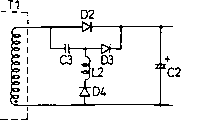
图11是表示本发明的另一个实施例的开关电源的主要部分的电路图;Fig. 11 is a circuit diagram showing a main part of a switching power supply of another embodiment of the present invention;
图12A是在图11所示的开关电源中的开关元件SW1的电压波形图;FIG. 12A is a voltage waveform diagram of the switching element SW1 in the switching power supply shown in FIG. 11;
图12B是在图11所示的开关电源中的开关元件SW1的电流波形图;Fig. 12B is a current waveform diagram of the switching element SW1 in the switching power supply shown in Fig. 11;
图12C是在图11所示的开关电源中的换向二极管D2的电流波形图;Fig. 12C is a current waveform diagram of the commutating diode D2 in the switching power supply shown in Fig. 11;
图13是表示开关电源的主要部分的电路图,用于说明每个部分中的电流响应;Fig. 13 is a circuit diagram showing the main parts of the switching power supply for explaining the current response in each part;
图14是表示开关电源的主要部分的电路图,用于说明每个部分中的电流响应;Fig. 14 is a circuit diagram showing the main parts of the switching power supply, for explaining the current response in each part;
图15是表示开关电源的主要部分的电路图,用于说明每个部分中的电流响应;Fig. 15 is a circuit diagram showing main parts of a switching power supply for explaining current response in each part;
图16是表示开关电源的主要部分的电路图,用于说明每个部分中的电流响应;Fig. 16 is a circuit diagram showing the main parts of the switching power supply, for explaining the current response in each part;
图17是表示开关电源的主要部分的电路图,用于说明每个部分中的电流响应;Fig. 17 is a circuit diagram showing the main parts of the switching power supply, for explaining the current response in each part;
图18是表示开关电源的主要部分的电路图,用于说明每个部分中的电流响应;Fig. 18 is a circuit diagram showing the main parts of the switching power supply for explaining the current response in each part;
图19是表示开关电源的主要部分的电路图,用于说明每个部分中的电流响应;Fig. 19 is a circuit diagram showing the main parts of the switching power supply, for explaining the current response in each part;
图20A是图13到图19所示的开关元件SW1的电压波形图;Fig. 20A is a voltage waveform diagram of the switching element SW1 shown in Fig. 13 to Fig. 19;
图20B是图13到图19所示的开关元件SW1的电流波形图;FIG. 20B is a current waveform diagram of the switching element SW1 shown in FIGS. 13 to 19;
图20C是图13到图19所示的换向二极管D2的电流波形图;Fig. 20C is a current waveform diagram of the commutation diode D2 shown in Fig. 13 to Fig. 19;
图20D是图13到图19所示的电容器C3的电流波形图;Figure 20D is a current waveform diagram of the capacitor C3 shown in Figure 13 to Figure 19;
图20E是图13到图19所示的电容器C3的电压波形图;Fig. 20E is a voltage waveform diagram of capacitor C3 shown in Fig. 13 to Fig. 19;
图20F是图13到图19所示的线圈L2的电流波形图;Fig. 20F is a current waveform diagram of the coil L2 shown in Fig. 13 to Fig. 19;
图21是表示本发明的另一个实施例的开关电源的主要部分的电路图;Fig. 21 is a circuit diagram showing a main part of a switching power supply of another embodiment of the present invention;
图22A是在图21所示的开关电源中的开关元件SW1的电压波形图;FIG. 22A is a voltage waveform diagram of the switching element SW1 in the switching power supply shown in FIG. 21;
图22B是在图21所示的开关电源中的开关元件SW1的电流波形图;FIG. 22B is a current waveform diagram of the switching element SW1 in the switching power supply shown in FIG. 21;
图22C是在图21所示的开关电源中的换向二极管D2的电流波形图;FIG. 22C is a current waveform diagram of the commutating diode D2 in the switching power supply shown in FIG. 21;
图23是表示开关电源的主要部分的电路图,用于说明每个部分中的电流响应;Fig. 23 is a circuit diagram showing the main parts of the switching power supply for explaining the current response in each part;
图24是表示开关电源的主要部分的电路图,用于说明每个部分中的电流响应;Fig. 24 is a circuit diagram showing the main parts of the switching power supply for explaining the current response in each part;
图25是表示开关电源的主要部分的电路图,用于说明每个部分中的电流响应;Fig. 25 is a circuit diagram showing the main parts of the switching power supply for explaining the current response in each part;
图26是表示开关电源的主要部分的电路图,用于说明每个部分中的电流响应;Fig. 26 is a circuit diagram showing the main parts of the switching power supply for explaining the current response in each part;
图27是表示开关电源的主要部分的电路图,用于说明每个部分中的电流响应;Fig. 27 is a circuit diagram showing the main parts of the switching power supply, for explaining the current response in each part;
图28是表示开关电源的主要部分的电路图,用于说明每个部分中的电流响应;Fig. 28 is a circuit diagram showing the main parts of the switching power supply, for explaining the current response in each part;
图29是表示开关电源的主要部分的电路图,用于说明每个部分中的电流响应;Fig. 29 is a circuit diagram showing the main parts of the switching power supply for explaining the current response in each part;
图30A是图23到图29所示的开关元件SW1的电压波形图;Fig. 30A is a voltage waveform diagram of the switching element SW1 shown in Fig. 23 to Fig. 29;
图30B是图23到图29所示的开关元件SW1的电流波形图;Fig. 30B is a current waveform diagram of the switching element SW1 shown in Fig. 23 to Fig. 29;
图30C是图23到图29所示的换向二极管D2的电流波形图;Fig. 30C is a current waveform diagram of the commutation diode D2 shown in Fig. 23 to Fig. 29;
图30D是图23到图29所示的电容器C3的电流波形图;Figure 30D is a current waveform diagram of the capacitor C3 shown in Figure 23 to Figure 29;
图30E是图23到图29所示的电容器C3的电压波形图;Figure 30E is a voltage waveform diagram of the capacitor C3 shown in Figure 23 to Figure 29;
图30F是图23到图29所示的线圈L2的电流波形图;Fig. 30F is a current waveform diagram of the coil L2 shown in Fig. 23 to Fig. 29;
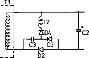
图31是表示本发明的另一个实施例的开关电源的主要部分的电路图;Fig. 31 is a circuit diagram showing a main part of a switching power supply according to another embodiment of the present invention;
图32是表示本发明的另一个实施例的开关电源的主要部分的电路图;Fig. 32 is a circuit diagram showing a main part of a switching power supply according to another embodiment of the present invention;
图33是表示本发明的另一个实施例的开关电源的主要部分的电路图;Fig. 33 is a circuit diagram showing a main part of a switching power supply according to another embodiment of the present invention;
图34是表示本发明的另一个实施例的开关电源的主要部分的电路图;34 is a circuit diagram showing a main part of a switching power supply according to another embodiment of the present invention;
图35是表示本发明的另一个实施例的开关电源的主要部分的电路图;Fig. 35 is a circuit diagram showing a main part of a switching power supply according to another embodiment of the present invention;
图36是表示本发明的另一个实施例的开关电源的主要部分的电路图;Fig. 36 is a circuit diagram showing a main part of a switching power supply according to another embodiment of the present invention;
图37是表示本发明的另一个实施例的开关电源的主要部分的电路图;Fig. 37 is a circuit diagram showing a main part of a switching power supply according to another embodiment of the present invention;
图38是表示本发明的另一个实施例的开关电源的主要部分的电路图;以及Fig. 38 is a circuit diagram showing a main part of a switching power supply of another embodiment of the present invention; and
图39是表示本发明的另一个实施例的开关电源的主要部分的电路图。Fig. 39 is a circuit diagram showing main parts of a switching power supply according to another embodiment of the present invention.
在所有这些图中,相同的元件用相同的标号表示。In all these figures, the same elements are indicated by the same reference numerals.
具体实施方式 Detailed ways
下面参照图1到图10说明按照本发明的优选实施例的缓冲电路的开关电源。所述开关电源是一种作为功率变换器的例子的正向方案(forwardscheme)。A switching power supply for a snubber circuit according to a preferred embodiment of the present invention will be described below with reference to FIGS. 1 to 10. FIG. The switching power supply is a forward scheme as an example of a power converter.
参见图1,一次侧的平波电容器C1对施加于其上的全波整流电压进行滤波。变换器变压器T1包括一次线圈和二次线圈,同时在变换器变压器T1中的漏感用L表示。开关元件SW1由晶体管构成,并和变换器变压器T1的一次线圈串联连接,通过导通和截止进行功率控制。Referring to Fig. 1, the smoothing capacitor C1 on the primary side filters the full-wave rectified voltage applied to it. The converter transformer T1 includes a primary coil and a secondary coil, while the leakage inductance in the converter transformer T1 is denoted by L. The switching element SW1 is composed of a transistor, is connected in series with the primary coil of the converter transformer T1, and performs power control by turning on and off.
整流二极管D1的阳极连接在变换器变压器T1的二次线圈的一端。扼流线圈L1和整流二极管D1的阴极串联连接。换句话说,扼流线圈L1通过整流二极管D1间接地和变换器变压器T1的二次线圈相连。扼流线圈L1作为平波磁性体,其在开关元件S1导通时存储能量,在开关元件S2截止时释放能量。The anode of the rectifier diode D1 is connected to one end of the secondary coil of the converter transformer T1. The choke coil L1 and the cathode of the rectifier diode D1 are connected in series. In other words, the choke coil L1 is indirectly connected to the secondary coil of the converter transformer T1 through the rectifier diode D1. The choke coil L1 is a flat-wave magnetic body, which stores energy when the switch element S1 is turned on, and releases energy when the switch element S2 is turned off.
换向二极管D2连接在整流二极管D1和扼流线圈L1的连接部分。换向二极管D2作为用于释放扼流线圈L1中的能量的二极管。二次侧平波电容C2和扼流线圈L1以及变换器变压器T1的二次线圈并联。The commutation diode D2 is connected to the connection portion between the rectifier diode D1 and the choke coil L1. The commutation diode D2 serves as a diode for discharging the energy in the choke coil L1. The secondary side smoothing capacitor C2 is connected in parallel with the choke coil L1 and the secondary coil of the converter transformer T1.
基本上按上述方式构成的正向方案开关电源的操作是熟知的,因此此处省略其详细说明。在这种情况下,开关电源是一种进行功率变换的电路方案,用于获得稳定的电流或电压,一般包括输出电压的检测电路,或控制器电路,用于按照检测的电压通过开关元件SW1的导通与截止周期的控制,把输出电压稳定地控制在恒值,不过,在本实施例中的图中没有示出这些电路。The operation of the forward scheme switching power supply basically constituted as described above is well known, and therefore its detailed description is omitted here. In this case, a switching power supply is a circuit scheme for power conversion, used to obtain a stable current or voltage, generally including an output voltage detection circuit, or a controller circuit, used to pass the switching element SW1 according to the detected voltage The control of the turn-on and turn-off periods can stably control the output voltage at a constant value, but these circuits are not shown in the figure of this embodiment.
缓冲电路10包括电容器C3和二极管D3的第一串联电路和线圈L2与二极管D4的第二串联电路。The
第一串联电路20和换向二极管D2并联连接。在第一串联电路20中,电容器C3连接在换向二极管D2中的连接扼流线圈侧(磁性体连接侧)“a”。在这种情况下,扼流线圈连接侧a相应于换向二极管D2的阴极侧。The
第二串联电路30连接在第一串联电路20中的电容器C3和二极管D3的连接部分b与扼流线圈L1的非连接换向二极管侧c之间。The
参见图2A-2D,在随着开关元件SW1的导通和截止而产生的电流和电压的波形中,开关元件SW1的电压VSW1的变化如图2A所示。开关元件SW1的电流ISW1的变化如图2B所示。整流二极管D1的电流ID1的变化如图2C所示。换向二极管D2的电流ID2的变化如图2D所示。Referring to FIGS. 2A-2D , among the waveforms of current and voltage generated as the switching element SW1 is turned on and off, the voltage V SW1 of the switching element SW1 varies as shown in FIG. 2A . The change of the current ISW1 of the switching element SW1 is shown in FIG. 2B. The change of the current I D1 of the rectifying diode D1 is shown in FIG. 2C . The variation of the current ID2 of the commutating diode D2 is shown in Fig. 2D.
参见图3和图10A-10F,按照模式式1到模式7说明在开关元件SW1截止时电压波动的抑制。Referring to FIG. 3 and FIGS. 10A-10F , the suppression of the voltage fluctuation when the switching element SW1 is turned off will be described in accordance with
在每种模式中,电流由箭头表示。In each mode, the current is indicated by an arrow.
图10A表示施加于开关元件SW1的电压VSW1(集电极电压),图10B表示流入开关元件SW1的电流ISW1,图10C表示流入换向二极管D2的电流ID2,图10D表示流入电容器C3的电流IC3,图10E表示施加于电容器C3的电压VC3,图10F表示流入线圈L2的电流IL2。Fig. 10A shows the voltage V SW1 (collector voltage) applied to the switching element SW1, Fig. 10B shows the current I SW1 flowing into the switching element SW1, Fig. 10C shows the current I D2 flowing into the commutating diode D2, and Fig. 10D shows the current I D2 flowing into the capacitor C3 The current I C3 , Fig. 10E shows the voltage V C3 applied to the capacitor C3, and Fig. 10F shows the current I L2 flowing in the coil L2.
(模式1)(mode 1)
在模式1中,如图3和图10A-10F所示,开关元件SW1在模式1开始时导通。因为开关元件SW1导通,其电压VSW1接近0,其电流ISW1近似为一个预定值的恒值。In
换向二极管D2的电流ID2为0。The current I D2 of the commutation diode D2 is zero.
从模式1开始到模式1的一半在电容器C3存储的能量较小的期间内电容器C3的电流IC3向负的方向增加,接着,随着存储能量的增加而减少,在模式1结束时,因电容器C3存储的能量已满而停止。From the beginning of
电容器C3的电压VC3向正的方向增加,直到模式1结束,线圈L2的电流IL2增加,然后在中途转为减少。The voltage V C3 of the capacitor C3 increases in the positive direction until the end of the
电流通过由变换器变压器T1的二次线圈、整流二极管D1和扼流线圈L1构成的第一通路以及由所述的二次线圈、电容器C3、线圈L2和二极管D4构成的第二通路流向平波电容器C2。The current flows to the flat wave through the first path formed by the secondary coil of the converter transformer T1, the rectifier diode D1 and the choke coil L1 and the second path formed by the secondary coil, the capacitor C3, the coil L2 and the diode D4 Capacitor C2.
(模式2)(mode 2)
在模式2中,如图4和图10A-10F所示,开关元件SW1的电压VSW1和电流ISW1和换向二极管D2的电流ID2根本不变。因为C3已经存储有能量,并且在全充电状态,所以电流IC3不再流入,因而电容器C3的电压VC3基本恒定。而线圈L2借助于其存储的能量作为电源流过电流IL2,即使来自电容器C3的电流截止。电流IL2逐渐减少,这是因为其能量减少的缘故。In
电流经过由变换器变压器T1的二次线圈、整流二极管D1和扼流线圈L1构成的第一通路以及由二极管D3、线圈L2和二极管D4构成的第二通路流向平波电容器C2。The current flows to the smoothing capacitor C2 through the first path formed by the secondary coil of the converter transformer T1, the rectifier diode D1 and the choke coil L1 and the second path formed by the diode D3, the coil L2 and the diode D4.
(模式3)(mode 3)
如图5和图10A-10F所示,当模式3开始时,开关元件SW1截止。由于截止,开关元件SW1的电压VSW1开始减少,而其电流ISW1则开始减少。As shown in FIG. 5 and FIGS. 10A-10F , when the
即使在模式3开始时,电流继续流入扼流圈L1。此外,换向二极管D2在模式3中不导通,电流ID2等于0。Even at the start of
在这种状态下,因为开关元件SW1是截止的,所以变换器变压器T1的二次线圈的电压减少。结果,存储在电容器C3中的电压更高,使得电流IC3从电容器C3流入扼流线圈L1。电流IC3逐渐增加,直到模式3结束。In this state, since the switching element SW1 is turned off, the voltage of the secondary coil of the converter transformer T1 decreases. As a result, the voltage stored in capacitor C3 is higher, so that current I C3 flows from capacitor C3 into choke coil L1. Current I C3 increases gradually until
因为电流IC3逐渐增加,所以在整个模式3中,开关元件SW1的电流ISW1逐渐地且平滑地减少,因而,在模式3中开关元件SW1的电压VSW1的波动被抑制。Since the current I C3 gradually increases, the current I SW1 of the switching element SW1 gradually and smoothly decreases throughout
电流通过由变换器变压器T1的二次线圈、整流二极管D1以及扼流线圈L1构成的第一通路、由二极管D3、电容器C3和扼流线圈L1构成的第二通路和由二极管D3、线圈L2以及二极管D4构成的第三通路流向平波电容器C2。The current passes through the first path formed by the secondary coil of the converter transformer T1, the rectifier diode D1 and the choke coil L1, the second path formed by the diode D3, the capacitor C3 and the choke coil L1, and the second path formed by the diode D3, the coil L2 and the choke coil L1. A third path formed by diode D4 flows to smoothing capacitor C2.
(模式4)(Mode 4)
参看图6和图10A-10F,虽开关元件SW1从开始到模式4的第一半个时间间隔期间处于截止状态,电流不通过整流二极管D1流入扼流线圈L1。Referring to FIG. 6 and FIGS. 10A-10F, although the switching element SW1 is in the OFF state from the start to the first half time interval of
虽然来自电容器C3的电流IC3流入扼流线圈L1,但电流IC3在整个模式4期间几乎是恒定的。相应地,电流ID2在整个模式4期间也不流入换向二极管D2。Although the current I C3 from the capacitor C3 flows into the choke coil L1, the current I C3 is almost constant during the
电流通过由二极管D3、电容器C3和扼流线圈L1构成的第一通路以及由二极管D3、线圈L2和二极管D4构成的第二通路流入平波电容器C2。Current flows into smoothing capacitor C2 through a first path formed by diode D3, capacitor C3 and choke coil L1 and a second path formed by diode D3, coil L2 and diode D4.
(模式5)(mode 5)
在模式5中,如图7和图10A-10F所示,来自电容器C3中的电流开始减少,使得换向二极管D2导通,从而把扼流线圈L1设置为电流源,借以使电流ID2开始流过。In
电流通过由换向二极管D2和扼流线圈L1构成的第一通路、由二极管D3、电容器C3和扼流线圈L1构成的第二通路以及由二极管D3、线圈L2和二极管D4构成的第二通路流入平波电容器C2。The current flows through the first path formed by commutation diode D2 and choke coil L1, the second path formed by diode D3, capacitor C3 and choke coil L1, and the second path formed by diode D3, coil L2 and diode D4. Smoothing capacitor C2.
(模式6)(Mode 6)
在模式6中,如图8和图10A-10F所示,来自电容器C3的电流IC3不再流动,并且流入换向二极管D2的电流ID2也几乎是恒定的。In
电流通过由换向二极管D2和扼流线圈L1构成的第一通路,以及由二极管D3、线圈L2和二极管D4构成的第三通路流入平波电容器C2。The current flows into smoothing capacitor C2 through a first path formed by commutating diode D2 and choke coil L1, and a third path formed by diode D3, coil L2 and diode D4.
(模式7)(Mode 7)
在模式7中,如图9和图10A-10F所示,开关元件SW1的电压VSW1也是稳定的。In
电流通过由换向二极管D2和扼流线圈L1构成的通路流入平波电容器C2。The current flows into the smoothing capacitor C2 through the path formed by the commutating diode D2 and the choke coil L1.
在上述的模式1到模式7中,在本发明的实施例的情况下,因为在模式3中在开关元件SW1截止时开关元件SW1的电流ISW1逐渐减少,所以即使变换器变压器T1的一次线圈具有大的漏感,也能抑制在开关元件SW1截止时的电压瞬变。In the above-mentioned
此外,因为由电容器C3、二极管D3和D4以及线圈L2形成缓冲电路10,所以基本上可以防止缓冲电路10中的能量消耗。Furthermore, since the
缓冲电路10提供在开关电源的二次侧中,借以使得能够使用额定电压和外形尺寸小的元件。The
下面参照图11到图20说明按照本发明的另一个实施例的回扫开关电源,所述开关电源具有缓冲电路10。和上述的实施例一样,缓冲电路具有由电容器C3和二极管D3构成的第一串联电路20,以及由线圈L2和二极管D4构成的第二串联电路30。Next, a flyback switching power supply having a
第一串联电路20和换向二极管D2并联连接。The
在第一串联电路20中,电容器C3和换向二极管D2中的变换器变压器T1中的连接二次线圈侧(磁性体连接侧)a相连。In the
第二串联电路30连接在第一串联电路20中的电容器C3和二极管D3的连接部分b和作为磁性体的二次线圈中的非连接换向二极管侧c之间。The
参见图12A-12C,如图12A和12B所示,其中分别示出了开关元件SW1的电压VSW1及其电流ISW1的变化。在图12C中示出了换向二极管D2的电流ID2的变化。Referring to FIGS. 12A-12C , as shown in FIGS. 12A and 12B , the changes of the voltage V SW1 of the switching element SW1 and its current IS SW1 are shown respectively. The variation of the current I D2 of the commutating diode D2 is shown in FIG. 12C .
图13到图19分别说明模式1到7。13 to 19 illustrate
图20A到20F分别相应于图10A到图10F。20A to 20F correspond to FIGS. 10A to 10F, respectively.
(模式1)(mode 1)
如图13和图20A-20F所示,在模式1开始,开关元件SW1导通。开关元件SW1上的电压VSW1接近于0,通过开关元件SW1的电流ISW1近似于一个恒定的预定值。换向二极管D2的电流ID2为0。As shown in FIG. 13 and FIGS. 20A-20F , at the start of
在缓冲电路10中,电容器C3的电流IC3向负的方向增加,然后在中途减少,最后,在模式1结束时停止流动,此时在电容器C3中存储的能量处于满状态。因为换向二极管D2截止,没有电流流过平波电容器C2。In the
(模式2)(mode 2)
在模式2中,如图14和图20A-20F所示,因为电容器C3已经存储有能量并处于满充电状态,所以电流IC3流动。线圈L2借助于在其中存储的能量而成为电流源,并且其中流过电流IL2。因而,电流通过由线圈L2、二极管D4和二极管D3构成的通路流入平波电容器C2。In
(模式3)(mode 3)
在模式3中,如图15和图20A-20F所示,开关元件SW1截止,开关元件SW1上的电压开始增加,并且其电流ISW1开始减少。In
在这种情况下,由于由电容器C3施加的电流IC3,从模式3开始到结束开关元件SW1的电流ISW1平滑地且逐渐地减少,使得开关元件SW1上的电压VSW1以这样一个梯度增加,使得从模式3开始到结束能够抑制电压瞬变。In this case, the current I SW1 of the switching element SW1 decreases smoothly and gradually from the beginning to the end of
相应地,电流通过由变换器变压器T1的二次线圈、电容器C3和二极管D3构成的通路和由线圈L2、二极管D4和二极管D3构成的通路流入平波电容器C2。Accordingly, current flows into the smoothing capacitor C2 through the path formed by the secondary coil of the converter transformer T1, the capacitor C3, and the diode D3, and the path formed by the coil L2, the diode D4, and the diode D3.
(模式4)(Mode 4)
参考图16和图20A-20F。在模式4中,电流通过由二次线圈、电容器C3和二极管D3构成的通路以及由线圈L2、二极管D4、和二极管D3构成的另一通路流入平波电容器C2。See Figure 16 and Figures 20A-20F. In
(模式5)(mode 5)
在模式5中,如图17和图20A-20F所示,电流ID2开始流入换向二极管D2,同时电容器C3的电流IC3开始减少。In
电流通过由二次线圈和换向二极管D2构成的通路,由二次线圈、电容器C3和二极管D3构成的通路以及由线圈L2、二极管D4和二极管D3构成的通路流入平波电容器C2。The current flows into the smoothing capacitor C2 through the path formed by the secondary coil and commutating diode D2, the path formed by the secondary coil, capacitor C3, and diode D3, and the path formed by coil L2, diode D4, and diode D3.
(模式6)(Mode 6)
在模式6中,如图18和图20A-20F所示,电流IC3不从电容器C3流动,并且电流通过由二次线圈和换向二极管D2构成的通路,以及由线圈L2、二极管D4和二极管D3构成的通路流入平波电容器C2。In
(模式7)(Mode 7)
在模式7中,如图19和图20A-20F所示,电流通过由换向二极管D2和二次线圈构成的通路流入平波电容器C2。In
在上述的实施例中,和前面所述的实施例一样,抑制了在开关元件SW1截止时的电压瞬变。In the above-described embodiment, the voltage transient when the switching element SW1 is turned off is suppressed as in the previously described embodiment.
此外,因为缓冲电路10具有电容器C3、二极管D3和D4,以及线圈L2,所以基本上可以防止缓冲电路10中的能量损失。Furthermore, since the
缓冲电路10提供在开关电源的二次侧中,因此能够使用额定电压和外形尺寸小的元件。The
参看图21-30说明按照本发明的另一个优选实施例的抽头电抗器方案的开关电源。所述开关电源包括一次侧平波电容器C1,开关元件SW1,抽头电抗器L3,二次侧平波电容C2,换向二极管D2和缓冲电路10。Referring to Figs. 21-30, a switching power supply according to a tapped reactor scheme according to another preferred embodiment of the present invention will be described. The switching power supply includes a primary side smoothing capacitor C1 , a switch element SW1 , a tapped reactor L3 , a secondary side smoothing capacitor C2 , a commutating diode D2 and a
开关电源的这种操作是熟知的,因此省略其说明。Such an operation of a switching power supply is well known, and thus its description is omitted.
所述开关电源具有缓冲电路10。和上述的实施例一样,缓冲电路10具有由电容器C3和二极管D3构成的第一串联电路20,和由线圈L2以及二极管D4构成的第二串联电路30。The switching power supply has a
第一串联电路20和换向二极管D2并联。The
在第一串联电路20中,电容器C3连接到换向二极管D2中的连接抽头电抗器侧(磁性体连接侧)a。在这种情况下,二次线圈连接侧a相应于换向二极管D2的阴极侧。In the
第二串联电路30串联在第一串联电路20中的电容器C3与二极管D3的连接部分b和抽头电抗器L3中的非连接换向二极管侧c之间。The
参照图22A-22C,开关元件SW1的电压VSW1如图22A所示,其电流ISW1如图22B所示。换向二极管D2的电流ID2如图22C所示。Referring to Figures 22A-22C, the voltage V SW1 of the switching element SW1 is shown in Figure 22A, and its current I SW1 is shown in Figure 22B. The current I D2 of the commutating diode D2 is shown in Fig. 22C.
图23-29分别表示模式1-模式7。Figures 23-29 represent Mode 1-
图30A-30F分别相应于图10A-10F。Figures 30A-30F correspond to Figures 10A-10F, respectively.
(模式1)(mode 1)
在模式1中,如图23和图30A-30F所示,开关元件SW1导通。开关元件SW1的电压VSW1接近于0,其电流ISW1近似于预定值的恒值。换向二极管D2的电流ID2是0。In
电容器C3的电流IC3向负的方向增加,然后减少,在模式1结束时,当电容器C3存储的能量处于满状态时,电流则停止流入电容器C3。The current I C3 of the capacitor C3 increases in the negative direction, then decreases, and at the end of
(模式2)(mode 2)
在模式2中,如图24和图30A-30F所示,开关元件SW1的电压VSW1和电流ISW1都不存在。因为电容器C3已经存储有能量,并处于满充电状态,所以没有电流IC3电容器C3。In
(模式3)(mode 3)
如图25和图30A-30F所示,模式3是开关元件SW1的完全截止周期。在模式3开始时,开关元件SW1的电压VSW1开始增加,并且其电流ISW1开始减少。As shown in Fig. 25 and Figs. 30A-30F,
在这种情况下,由于从电容器C3提供的电流IC3,从模式3的开始到结束开关元件SW1的电流ISW1平滑地且逐渐地减少,使得开关元件SW1的电压VSW1以这样的梯度增加,在所述梯度下,从模式3的开始到结束,电压瞬变被抑制。In this case, the current I SW1 of the switching element SW1 decreases smoothly and gradually from the start to the end of
(模式4)(Mode 4)
在模式4中,如图26和图30A-30F所示,电流通过由二极管D3、电容器C3和抽头电抗器L3的另一个线圈L32构成的第一通路和由二极管D3、线圈L2和二极管D4构成的第二通路流入平波电容器C3。In
(模式5)(mode 5)
在模式5中,如图27和图30A-30F所示,电流ID2开始流入换向二极管D2,同时电容器C3的电流IC3开始减少。In
电流通过由换向二极管D2和抽头电抗器L3的另一个线圈L32构成的第一通路,由二极管D3、电容器C3和抽头电抗器L3的另一个线圈构成的第二通路,以及由二极管D3、线圈L2和二极管D4构成的第三通路流入平波电容器C2。The current passes through the first path formed by the commutating diode D2 and the other coil L32 of the tapped reactor L3, the second path formed by the diode D3, the capacitor C3 and the other coil of the tapped reactor L3, and by the diode D3, the coil The third path formed by L2 and diode D4 flows into smoothing capacitor C2.
(模式6)(Mode 6)
在模式6中,如图28和图30A-30F所示,电流IC3不再从电容器C3中流动。In
电流通过由换向二极管D2和抽头电抗器L3的另一个线圈L32构成的第一通路,以及由二极管D3、线圈L2和二极管D4构成的第二通路流入平波电容器C2。The current flows into smoothing capacitor C2 through a first path formed by commutating diode D2 and another coil L32 of tapped reactor L3, and a second path formed by diode D3, coil L2 and diode D4.
(模式7)(Mode 7)
在模式7中,如图29和图30A-30F所示,电流通过由换向二极管D2和抽头电抗器L3的另一个线圈L32构成的通路流入平波电容器C2。In
本实施例可以获得和上述相同的操作效果。This embodiment can obtain the same operation effect as above.
此外,本发明的正向方案开关电源的例子包括如图31-33所示的那些。本发明同样可以应用于这些开关电源。在图31-33中,没有示出变换器变压器T1的一次侧。此外,在图32和33的情况下,扼流线圈L1和变换器变压器T1的二次线圈直接相连。In addition, examples of the forward scheme switching power supply of the present invention include those shown in Figs. 31-33. The present invention is equally applicable to these switching power supplies. In Figs. 31-33, the primary side of the converter transformer T1 is not shown. Furthermore, in the case of FIGS. 32 and 33, the choke coil L1 and the secondary coil of the converter transformer T1 are directly connected.
本发明的回扫方案开关电源的例子包括图34-36所示的那些。本发明同样可以应用于这些开关电源。在图34-36中,没有示出变换器变压器T1的一次侧。Examples of flyback scheme switching power supplies of the present invention include those shown in FIGS. 34-36. The present invention is equally applicable to these switching power supplies. In Figs. 34-36, the primary side of converter transformer T1 is not shown.
本发明的抽头电抗器方案开关电源的例子如图37到39所示。本发明同样适用于这些开关电源。图37到39中没有示出开关元件SW1。Examples of the tapped reactor scheme switching power supply of the present invention are shown in FIGS. 37 to 39 . The present invention is equally applicable to these switching power supplies. The switching element SW1 is not shown in FIGS. 37 to 39 .
本发明作为功率变换器适用于开关电源。但是,这并不意味着限制本发明的范围。本发明也可以应用于功率变换器,例如逆变器。The invention is suitable for switching power supply as a power converter. However, this is not meant to limit the scope of the invention. The invention can also be applied to power converters, such as inverters.
虽然已经说明了目前认为是优选的本发明的实施例,应当理解,其中可以作出各种改型,这些改型都落在所附的权利要求的构思和范围内。While there have been described what are presently considered to be the preferred embodiments of the invention, it should be understood that various modifications may be made therein which will fall within the spirit and scope of the appended claims.
Claims (8)
Applications Claiming Priority (6)
| Application Number | Priority Date | Filing Date | Title |
|---|---|---|---|
| JP316633/00 | 2000-10-17 | ||
| JP316633/2000 | 2000-10-17 | ||
| JP2000316633A JP2002125370A (en) | 2000-10-17 | 2000-10-17 | Snubber circuit |
| JP189447/2001 | 2001-06-22 | ||
| JP2001189447A JP2003009527A (en) | 2001-06-22 | 2001-06-22 | Snubber circuit and power converter using the same |
| JP189447/01 | 2001-06-22 |
Publications (2)
| Publication Number | Publication Date |
|---|---|
| CN1349297A CN1349297A (en) | 2002-05-15 |
| CN1193488C true CN1193488C (en) | 2005-03-16 |
Family
ID=26602234
Family Applications (1)
| Application Number | Title | Priority Date | Filing Date |
|---|---|---|---|
| CNB011385669A Expired - Fee Related CN1193488C (en) | 2000-10-17 | 2001-10-17 | Buffer circuit, and power conversion device using same |
Country Status (8)
| Country | Link |
|---|---|
| US (1) | US6507502B2 (en) |
| EP (1) | EP1202440B1 (en) |
| KR (1) | KR100425286B1 (en) |
| CN (1) | CN1193488C (en) |
| AT (1) | ATE349098T1 (en) |
| CA (1) | CA2358835C (en) |
| DE (1) | DE60125310T8 (en) |
| TW (1) | TWI237437B (en) |
Cited By (1)
| Publication number | Priority date | Publication date | Assignee | Title |
|---|---|---|---|---|
| CN106533183A (en) * | 2016-12-23 | 2017-03-22 | 天津大学 | Efficient isolation type DC full-bridge conversion circuit |
Families Citing this family (31)
| Publication number | Priority date | Publication date | Assignee | Title |
|---|---|---|---|---|
| US6569432B1 (en) * | 1995-02-24 | 2003-05-27 | Sloan-Kettering Institute For Cancer Research | Prostate-specific membrane antigen and uses thereof |
| AU717937B2 (en) | 1995-02-24 | 2000-04-06 | Sloan-Kettering Institute For Cancer Research | Prostate-specific membrane antigen and uses thereof |
| US20040253246A1 (en) * | 1996-02-23 | 2004-12-16 | Israeli Ron S. | Prostate-specific membrane antigen and uses thereof |
| CN100369371C (en) * | 2002-09-21 | 2008-02-13 | 中兴通讯股份有限公司 | A Circuit for Suppressing Reverse Spike Voltage of Diode |
| DE102004050060B4 (en) * | 2004-10-13 | 2018-02-08 | Osram Gmbh | Buck converter circuit |
| US6980447B1 (en) | 2004-10-18 | 2005-12-27 | Artesyn Technologies, Inc. | Active snubber circuit for synchronous rectifier |
| JP4884665B2 (en) * | 2004-11-12 | 2012-02-29 | ローム株式会社 | DC-AC converter, its controller IC, and DC-AC converter parallel operation system |
| KR100704976B1 (en) * | 2005-11-07 | 2007-04-09 | 삼성전기주식회사 | Half bridge DC-DC converter with voltage clamp circuit |
| AT503964B1 (en) * | 2007-01-23 | 2008-02-15 | Siemens Ag Oesterreich | Relief circuit arrangement for use in switched mode power supply, has precharging circuit charging capacitor more strongly than excessive voltage of diode while diode is switched in blocking direction with regard to amount |
| RU2368058C1 (en) * | 2008-05-06 | 2009-09-20 | Закрытое акционерное общество "Малое многопрофильное предприятие -ИРБИС" (ЗАО "ММП-ИРБИС") | Damping circuit for dc-to-dc converter |
| US8503201B2 (en) * | 2009-12-03 | 2013-08-06 | Schneider Electric It Corporation | Transient clamping circuitry for voltage converter |
| WO2012120600A1 (en) * | 2011-03-04 | 2012-09-13 | 三菱電機株式会社 | Power conversion device and refrigeration/ac system |
| JP5641368B2 (en) | 2012-04-12 | 2014-12-17 | 株式会社村田製作所 | Switching power supply |
| US10459464B2 (en) | 2012-09-03 | 2019-10-29 | Schneider Electric It Corporation | Method and apparatus for controlling distribution of power |
| EP2713488B1 (en) | 2012-09-28 | 2020-04-15 | OSRAM GmbH | Electronic converter, and related lighting system and method of operating an electronic converter |
| DE102012219526A1 (en) * | 2012-10-25 | 2014-04-30 | Siemens Aktiengesellschaft | Flyback converter has capacitor and diode between which connecting point is provided, and series arrangement of choke coil and third diode that is located in output terminals |
| CN103856081B (en) * | 2012-12-06 | 2016-08-10 | 东林科技股份有限公司 | DC-AC conversion device and power factor correction function method thereof |
| CN103856054A (en) * | 2012-12-06 | 2014-06-11 | 东林科技股份有限公司 | Isolated power conversion device and power conversion method thereof |
| CN105144562B (en) * | 2013-05-21 | 2017-10-31 | 株式会社村田制作所 | Switching power unit |
| EP2822166B1 (en) * | 2013-07-01 | 2016-04-06 | Siemens Aktiengesellschaft | Forward converter with snubber circuit at the secondary side |
| TWI504127B (en) * | 2013-11-01 | 2015-10-11 | Hep Tech Co Ltd | Isolated AC / DC converter and its conversion method |
| CN104638947A (en) * | 2013-11-14 | 2015-05-20 | 东林科技股份有限公司 | Isolation type alternating current and direct current conversion device and conversion method thereof |
| CN104682733B (en) * | 2013-11-27 | 2017-03-22 | 东林科技股份有限公司 | Flyback type alternating-current and direct-current conversion device and conversion method thereof |
| CN104682720A (en) * | 2013-11-29 | 2015-06-03 | 东林科技股份有限公司 | Alternating current-alternating current power supply conversion device and conversion method thereof |
| KR101683994B1 (en) * | 2014-11-05 | 2016-12-08 | 현대자동차주식회사 | DC-DC converter circuit |
| DE102016200662A1 (en) * | 2016-01-20 | 2017-07-20 | Robert Bosch Gmbh | Bidirectional DC / DC converter and method for charging the DC link capacitor of a DC / DC converter from the low-voltage battery |
| TWI624145B (en) * | 2016-08-12 | 2018-05-11 | 韋景川 | Energy adapter with primary side & secondary side synchronization tracking function |
| CN106954312B (en) * | 2017-04-28 | 2018-11-02 | 广东工业大学 | A kind of current balance LED drive circuit |
| CN107248812B (en) * | 2017-07-13 | 2023-06-27 | 天宝电子(惠州)有限公司 | A Soft Switching Flyback Converter |
| US12184163B2 (en) * | 2019-05-28 | 2024-12-31 | Ngai Kit Franki Poon | Switching power supply apparatus |
| TWI819586B (en) * | 2022-04-29 | 2023-10-21 | 亞源科技股份有限公司 | Full-bridge phase shift converter with voltage clamping |
Family Cites Families (11)
| Publication number | Priority date | Publication date | Assignee | Title |
|---|---|---|---|---|
| US4805079A (en) * | 1986-05-06 | 1989-02-14 | U.S. Philips Corp. | Switched voltage converter |
| JP2674341B2 (en) * | 1991-03-27 | 1997-11-12 | 三菱電機株式会社 | Snubber circuit of power converter |
| JPH05260739A (en) * | 1992-03-11 | 1993-10-08 | Nec Corp | Forward converter |
| GB9206020D0 (en) * | 1992-03-19 | 1992-04-29 | Astec Int Ltd | Transition resonant convertor |
| US5418709A (en) * | 1993-03-24 | 1995-05-23 | The United States Of America As Represented By The Administrator Of The National Aeronautics And Space Administration | Forback DC-to-DC converter |
| ATE179843T1 (en) * | 1994-02-10 | 1999-05-15 | Koninkl Philips Electronics Nv | HIGH FREQUENCY AC CONVERTER WITH POWER FACTOR CORRECTION |
| US5636114A (en) * | 1995-11-30 | 1997-06-03 | Electronic Measurements, Inc. | Lossless snubber circuit for use in power converters |
| DE19611707A1 (en) * | 1996-03-25 | 1997-10-02 | Patent Treuhand Ges Fuer Elektrische Gluehlampen Mbh | DC chopper |
| JPH11299237A (en) * | 1998-04-16 | 1999-10-29 | Nippon Electric Ind Co Ltd | Forward converter with active clamping circuit |
| US6052294A (en) * | 1998-09-14 | 2000-04-18 | Lucent Technologies Inc. | Power supply snubber reset circuit |
| JP3400443B2 (en) * | 1999-06-22 | 2003-04-28 | ティーディーケイ株式会社 | Switching power supply |
-
2001
- 2001-10-05 DE DE60125310T patent/DE60125310T8/en active Active
- 2001-10-05 AT AT01123890T patent/ATE349098T1/en not_active IP Right Cessation
- 2001-10-05 EP EP01123890A patent/EP1202440B1/en not_active Expired - Lifetime
- 2001-10-12 TW TW090125227A patent/TWI237437B/en not_active IP Right Cessation
- 2001-10-15 US US09/976,057 patent/US6507502B2/en not_active Expired - Fee Related
- 2001-10-16 KR KR10-2001-0063614A patent/KR100425286B1/en not_active Expired - Fee Related
- 2001-10-16 CA CA002358835A patent/CA2358835C/en not_active Expired - Fee Related
- 2001-10-17 CN CNB011385669A patent/CN1193488C/en not_active Expired - Fee Related
Cited By (1)
| Publication number | Priority date | Publication date | Assignee | Title |
|---|---|---|---|---|
| CN106533183A (en) * | 2016-12-23 | 2017-03-22 | 天津大学 | Efficient isolation type DC full-bridge conversion circuit |
Also Published As
| Publication number | Publication date |
|---|---|
| ATE349098T1 (en) | 2007-01-15 |
| US6507502B2 (en) | 2003-01-14 |
| CN1349297A (en) | 2002-05-15 |
| KR100425286B1 (en) | 2004-03-30 |
| US20020044459A1 (en) | 2002-04-18 |
| DE60125310D1 (en) | 2007-02-01 |
| CA2358835C (en) | 2004-06-22 |
| EP1202440A1 (en) | 2002-05-02 |
| EP1202440B1 (en) | 2006-12-20 |
| DE60125310T2 (en) | 2007-07-19 |
| CA2358835A1 (en) | 2002-04-17 |
| KR20020030716A (en) | 2002-04-25 |
| TWI237437B (en) | 2005-08-01 |
| DE60125310T8 (en) | 2007-10-25 |
Similar Documents
| Publication | Publication Date | Title |
|---|---|---|
| CN1193488C (en) | Buffer circuit, and power conversion device using same | |
| CN1302610C (en) | DC-DC converter | |
| CN101051789A (en) | Unidirectional DC-DC Converter | |
| CN1249904C (en) | Switch power source | |
| CN1241317C (en) | Switch power-supply device | |
| CN1260876C (en) | Switching mains | |
| CN1182648C (en) | switching power supply circuit | |
| CN1303749C (en) | Switching mains | |
| CN1224161C (en) | Switching power supply device | |
| CN1606395A (en) | Drive system and AC conversion apparatus | |
| CN101039080A (en) | Switching power supply circuit | |
| CN1171505C (en) | Magnetron drive power | |
| CN101056067A (en) | Switching power supply circuit | |
| CN1266821C (en) | Switch power-supply circuit | |
| CN1318896A (en) | Switch power circuit | |
| CN1726631A (en) | Switching power supply device and method for controlling switching power supply device | |
| CN1595759A (en) | Circuit for controlling battery charging, battery charging device and control method | |
| CN1521930A (en) | Switching power supply unit | |
| CN1732614A (en) | Switching power supply circuit | |
| CN1841582A (en) | Magnetic element and power supply | |
| CN1801592A (en) | Switching power supply circuit | |
| CN1881771A (en) | Switching power source circuit | |
| CN1759525A (en) | Switching power supply device | |
| CN1819428A (en) | Switching power supply circuit | |
| CN1848652A (en) | Switching power supply device and switching method |
Legal Events
| Date | Code | Title | Description |
|---|---|---|---|
| C10 | Entry into substantive examination | ||
| SE01 | Entry into force of request for substantive examination | ||
| C06 | Publication | ||
| PB01 | Publication | ||
| C14 | Grant of patent or utility model | ||
| GR01 | Patent grant | ||
| CF01 | Termination of patent right due to non-payment of annual fee |
Granted publication date: 20050316 Termination date: 20141017 |
|
| EXPY | Termination of patent right or utility model |