CN1801592A - Switching power supply circuit - Google Patents
Switching power supply circuit Download PDFInfo
- Publication number
- CN1801592A CN1801592A CNA2005100975905A CN200510097590A CN1801592A CN 1801592 A CN1801592 A CN 1801592A CN A2005100975905 A CNA2005100975905 A CN A2005100975905A CN 200510097590 A CN200510097590 A CN 200510097590A CN 1801592 A CN1801592 A CN 1801592A
- Authority
- CN
- China
- Prior art keywords
- switching
- circuit
- voltage
- secondary side
- rectification
- Prior art date
- Legal status (The legal status is an assumption and is not a legal conclusion. Google has not performed a legal analysis and makes no representation as to the accuracy of the status listed.)
- Granted
Links
Images


Classifications
-
- A—HUMAN NECESSITIES
- A61—MEDICAL OR VETERINARY SCIENCE; HYGIENE
- A61H—PHYSICAL THERAPY APPARATUS, e.g. DEVICES FOR LOCATING OR STIMULATING REFLEX POINTS IN THE BODY; ARTIFICIAL RESPIRATION; MASSAGE; BATHING DEVICES FOR SPECIAL THERAPEUTIC OR HYGIENIC PURPOSES OR SPECIFIC PARTS OF THE BODY
- A61H39/00—Devices for locating or stimulating specific reflex points of the body for physical therapy, e.g. acupuncture
- A61H39/04—Devices for pressing such points, e.g. Shiatsu or Acupressure
-
- H—ELECTRICITY
- H02—GENERATION; CONVERSION OR DISTRIBUTION OF ELECTRIC POWER
- H02M—APPARATUS FOR CONVERSION BETWEEN AC AND AC, BETWEEN AC AND DC, OR BETWEEN DC AND DC, AND FOR USE WITH MAINS OR SIMILAR POWER SUPPLY SYSTEMS; CONVERSION OF DC OR AC INPUT POWER INTO SURGE OUTPUT POWER; CONTROL OR REGULATION THEREOF
- H02M3/00—Conversion of DC power input into DC power output
- H02M3/22—Conversion of DC power input into DC power output with intermediate conversion into AC
- H02M3/24—Conversion of DC power input into DC power output with intermediate conversion into AC by static converters
- H02M3/28—Conversion of DC power input into DC power output with intermediate conversion into AC by static converters using discharge tubes with control electrode or semiconductor devices with control electrode to produce the intermediate AC
- H02M3/325—Conversion of DC power input into DC power output with intermediate conversion into AC by static converters using discharge tubes with control electrode or semiconductor devices with control electrode to produce the intermediate AC using devices of a triode or a transistor type requiring continuous application of a control signal
- H02M3/335—Conversion of DC power input into DC power output with intermediate conversion into AC by static converters using discharge tubes with control electrode or semiconductor devices with control electrode to produce the intermediate AC using devices of a triode or a transistor type requiring continuous application of a control signal using semiconductor devices only
- H02M3/338—Conversion of DC power input into DC power output with intermediate conversion into AC by static converters using discharge tubes with control electrode or semiconductor devices with control electrode to produce the intermediate AC using devices of a triode or a transistor type requiring continuous application of a control signal using semiconductor devices only in a self-oscillating arrangement
- H02M3/3385—Conversion of DC power input into DC power output with intermediate conversion into AC by static converters using discharge tubes with control electrode or semiconductor devices with control electrode to produce the intermediate AC using devices of a triode or a transistor type requiring continuous application of a control signal using semiconductor devices only in a self-oscillating arrangement with automatic control of output voltage or current
-
- H—ELECTRICITY
- H02—GENERATION; CONVERSION OR DISTRIBUTION OF ELECTRIC POWER
- H02M—APPARATUS FOR CONVERSION BETWEEN AC AND AC, BETWEEN AC AND DC, OR BETWEEN DC AND DC, AND FOR USE WITH MAINS OR SIMILAR POWER SUPPLY SYSTEMS; CONVERSION OF DC OR AC INPUT POWER INTO SURGE OUTPUT POWER; CONTROL OR REGULATION THEREOF
- H02M1/00—Details of apparatus for conversion
- H02M1/10—Arrangements incorporating converting means for enabling loads to be operated at will from different kinds of power supplies, e.g. from AC or DC
-
- A—HUMAN NECESSITIES
- A61—MEDICAL OR VETERINARY SCIENCE; HYGIENE
- A61H—PHYSICAL THERAPY APPARATUS, e.g. DEVICES FOR LOCATING OR STIMULATING REFLEX POINTS IN THE BODY; ARTIFICIAL RESPIRATION; MASSAGE; BATHING DEVICES FOR SPECIAL THERAPEUTIC OR HYGIENIC PURPOSES OR SPECIFIC PARTS OF THE BODY
- A61H2201/00—Characteristics of apparatus not provided for in the preceding codes
- A61H2201/01—Constructive details
- A61H2201/0119—Support for the device
-
- A—HUMAN NECESSITIES
- A61—MEDICAL OR VETERINARY SCIENCE; HYGIENE
- A61H—PHYSICAL THERAPY APPARATUS, e.g. DEVICES FOR LOCATING OR STIMULATING REFLEX POINTS IN THE BODY; ARTIFICIAL RESPIRATION; MASSAGE; BATHING DEVICES FOR SPECIAL THERAPEUTIC OR HYGIENIC PURPOSES OR SPECIFIC PARTS OF THE BODY
- A61H2201/00—Characteristics of apparatus not provided for in the preceding codes
- A61H2201/12—Driving means
- A61H2201/1253—Driving means driven by a human being, e.g. hand driven
- A61H2201/1261—Driving means driven by a human being, e.g. hand driven combined with active exercising of the patient
- A61H2201/1269—Passive exercise driven by movement of healthy limbs
-
- A—HUMAN NECESSITIES
- A61—MEDICAL OR VETERINARY SCIENCE; HYGIENE
- A61H—PHYSICAL THERAPY APPARATUS, e.g. DEVICES FOR LOCATING OR STIMULATING REFLEX POINTS IN THE BODY; ARTIFICIAL RESPIRATION; MASSAGE; BATHING DEVICES FOR SPECIAL THERAPEUTIC OR HYGIENIC PURPOSES OR SPECIFIC PARTS OF THE BODY
- A61H2201/00—Characteristics of apparatus not provided for in the preceding codes
- A61H2201/16—Physical interface with patient
- A61H2201/1683—Surface of interface
- A61H2201/1685—Surface of interface interchangeable
-
- A—HUMAN NECESSITIES
- A61—MEDICAL OR VETERINARY SCIENCE; HYGIENE
- A61H—PHYSICAL THERAPY APPARATUS, e.g. DEVICES FOR LOCATING OR STIMULATING REFLEX POINTS IN THE BODY; ARTIFICIAL RESPIRATION; MASSAGE; BATHING DEVICES FOR SPECIAL THERAPEUTIC OR HYGIENIC PURPOSES OR SPECIFIC PARTS OF THE BODY
- A61H2205/00—Devices for specific parts of the body
- A61H2205/12—Feet
- A61H2205/125—Foot reflex zones
-
- Y—GENERAL TAGGING OF NEW TECHNOLOGICAL DEVELOPMENTS; GENERAL TAGGING OF CROSS-SECTIONAL TECHNOLOGIES SPANNING OVER SEVERAL SECTIONS OF THE IPC; TECHNICAL SUBJECTS COVERED BY FORMER USPC CROSS-REFERENCE ART COLLECTIONS [XRACs] AND DIGESTS
- Y02—TECHNOLOGIES OR APPLICATIONS FOR MITIGATION OR ADAPTATION AGAINST CLIMATE CHANGE
- Y02B—CLIMATE CHANGE MITIGATION TECHNOLOGIES RELATED TO BUILDINGS, e.g. HOUSING, HOUSE APPLIANCES OR RELATED END-USER APPLICATIONS
- Y02B70/00—Technologies for an efficient end-user side electric power management and consumption
- Y02B70/10—Technologies improving the efficiency by using switched-mode power supplies [SMPS], i.e. efficient power electronics conversion e.g. power factor correction or reduction of losses in power supplies or efficient standby modes
Landscapes
- Power Engineering (AREA)
- Engineering & Computer Science (AREA)
- Health & Medical Sciences (AREA)
- Rehabilitation Therapy (AREA)
- Animal Behavior & Ethology (AREA)
- Life Sciences & Earth Sciences (AREA)
- Physical Education & Sports Medicine (AREA)
- General Health & Medical Sciences (AREA)
- Public Health (AREA)
- Veterinary Medicine (AREA)
- Pain & Pain Management (AREA)
- Epidemiology (AREA)
- Dc-Dc Converters (AREA)
Abstract
本发明提供了适应宽范围的开关电源电路,其采用开关频率变化控制,并在使用大AC输入电压时,可提高其AC到DC电源变换效率。通过在初级侧和次级侧上都提供串联谐振电路,形成采用绝缘变换器变压器PIT电磁耦合的耦合谐振电路。为在耦合谐振电路中获得单峰输出特性,绝缘变换器变压器PIT的磁芯中形成的间隙G的间隙长度被设置为约2.0mm,耦合系数k被设置为约0.8或更小。从而,可缩窄开关频率可变控制范围。另外,初级侧和次级侧谐振电路的谐振频率fo1和fo2被设置为使得至少当AC输入电压VAC是100V且负载功率是最大负载功率时,在初级侧串联谐振电流与次级侧整流电流之间出现所需相移。因此,当AC输入电压VAC是230V时,可提高AC到DC电源变换效率。

The invention provides a switching power supply circuit adaptable to a wide range, which adopts switching frequency change control, and can improve its AC to DC power conversion efficiency when using a large AC input voltage. By providing a series resonant circuit on both the primary side and the secondary side, a coupled resonant circuit using the electromagnetic coupling of the insulating converter transformer PIT is formed. To obtain single-peak output characteristics in the coupled resonance circuit, the gap length of the gap G formed in the magnetic core of the insulating converter transformer PIT is set to about 2.0 mm, and the coupling coefficient k is set to about 0.8 or less. Thus, the switching frequency variable control range can be narrowed. In addition, the resonance frequencies fo1 and fo2 of the primary side and secondary side resonance circuits are set so that at least when the AC input voltage VAC is 100 V and the load power is the maximum load power, there is a difference between the primary side series resonance current and the secondary side rectified current the desired phase shift occurs. Therefore, when the AC input voltage VAC is 230V, the AC-to-DC power conversion efficiency can be improved.
Description
技术领域technical field
本发明涉及作为电源被包括在各种电子装置中的开关电源电路。The present invention relates to a switching power supply circuit included as a power supply in various electronic devices.
背景技术Background technique
本发明的受让人已经提出了在初级侧上包括有谐振变换器的各种电源电路。日本专利申请早期公开No.2003-235259公开了所提出的电源电路的一个示例。The assignee of the present invention has proposed various power supply circuits including a resonant converter on the primary side. One example of the proposed power supply circuit is disclosed in Japanese Patent Application Laid-Open No. 2003-235259.
图12是图示了开关电源电路的一个示例的电路图,该开关电源电路包括谐振变换器,并且是基于本受让人已经递交的发明中的任一个来构造的。FIG. 12 is a circuit diagram illustrating one example of a switching power supply circuit including a resonant converter and constructed based on any one of the inventions already filed by the present assignee.
图12所示的电源电路中的开关变换器具有这样的配置:其中由半桥连接构成的他激(separately excited)电源谐振变换器与仅在开关操作中的关断时刻执行电压谐振操作的部分电压谐振电路相结合。The switching converter in the power supply circuit shown in Fig. 12 has a configuration in which a separately excited power resonant converter constituted by a half-bridge connection and a part that performs a voltage resonance operation only at the turn-off time in switching operation combined with a voltage resonant circuit.
在图12所示的电源电路中,耦合到商用交流电源AC的是由两个滤波电容器CL和一个共模扼流圈CMC形成的共模噪声滤波器。In the power supply circuit shown in FIG. 12, coupled to the commercial AC power supply AC is a common mode noise filter formed by two smoothing capacitors CL and a common mode choke coil CMC.
作为用于从来自商用交流电源AC的AC输入电压VAC产生DC输入电压的整流和平滑电路,由桥式整流电路Di和平滑电容器Ci形成的全波整流电路被提供在共模噪声滤波器的下游。As a rectification and smoothing circuit for generating a DC input voltage from an AC input voltage VAC from a commercial AC power supply AC, a full-wave rectification circuit formed of a bridge rectification circuit Di and a smoothing capacitor Ci is provided downstream of the common mode noise filter .
来自桥式整流电路Di的整流输出被充电到平滑电容器Ci中,结果,在平滑电容器Ci两端获得了电平与AC输入电压VAC的电平相等的经整流和平滑的电压Ei(DC输入电压)。The rectified output from the bridge rectification circuit Di is charged into the smoothing capacitor Ci, and as a result, a rectified and smoothed voltage Ei (the DC input voltage ).
作为被馈送了DC输入电压并执行开关操作的电流谐振变换器,提供了开关电路系统,其中由MOS-FET形成的两个开关元件Q1和Q2通过半桥连接而彼此相连,如图所示。由体二极管(body diode)形成的阻尼二极管DD1和DD2分别与开关元件Q1和Q2的漏极与源极之间的沟道并联连接,具有如图所示的阳极到阴极方向。As a current resonant converter fed with a DC input voltage and performing a switching operation, there is provided a switching circuit system in which two switching elements Q1 and Q2 formed of MOS-FETs are connected to each other by a half-bridge connection as shown. Damper diodes DD1 and DD2 formed by body diodes are connected in parallel with the channels between the drains and sources of switching elements Q1 and Q2 respectively, having an anode-to-cathode orientation as shown.
此外,部分谐振电容器Cp与开关元件Q2的漏极与源极之间的沟道并联连接。部分谐振电容器Cp的电容和初级绕组N1的漏电感L1形成并联谐振电路(部分电压谐振电路)。该部分电压谐振电路允许这样的部分电压谐振操作:其中仅当开关元件Q1和Q2关断时出现电压谐振。In addition, the partial resonance capacitor Cp is connected in parallel with the channel between the drain and the source of the switching element Q2. The capacitance of the partial resonance capacitor Cp and the leakage inductance L1 of the primary winding N1 form a parallel resonance circuit (partial voltage resonance circuit). This partial voltage resonance circuit allows a partial voltage resonance operation in which voltage resonance occurs only when the switching elements Q1 and Q2 are turned off.
电源电路具有例如由通用IC形成的振荡和驱动电路2,以便对开关元件Q1和Q2进行开关驱动。振荡和驱动电路2包括振荡电路和驱动电路,并向开关元件Q1和Q2的栅极施加具有所需频率的驱动信号(栅极电压)。从而,开关元件Q1和Q2实现开关操作,使得它们以所需的开关频率交替地导通/关断。The power supply circuit has, for example, an oscillation and
绝缘变换器变压器(isolated converter transformer)PIT(电源隔离变压器(Power Isolation Transformer))将来自开关元件Q1和Q2的开关输出传递到次级侧。An isolated converter transformer (PIT) (Power Isolation Transformer) transfers switching outputs from switching elements Q1 and Q2 to the secondary side.
经由初级侧串联谐振电容器C1,绝缘变换器变压器PIT的初级绕组N1的一端被耦合到开关元件Q1的源极与开关元件Q2的漏极之间的连接节点(开关输出节点),使得可以获取开关输出。One end of the primary winding N1 of the insulating converter transformer PIT is coupled to a connection node (switching output node) between the source of the switching element Q1 and the drain of the switching element Q2 via the primary side series resonance capacitor C1, so that switching output.
如图所示,初级绕组N1的另一端连接到初级侧的地。As shown, the other end of the primary winding N1 is connected to the ground on the primary side.
串联谐振电容器C1与初级绕组N1串联连接。串联谐振电容器C1的电容和绝缘变换器变压器PIT中的初级绕组N1(串联谐振绕组)的漏电感L1形成了初级侧串联谐振电路,其提供作为开关变换器操作的电流谐振操作。A series resonance capacitor C1 is connected in series with the primary winding N1. The capacitance of the series resonant capacitor C1 and the leakage inductance L1 of the primary winding N1 (series resonant winding) in the insulating converter transformer PIT form a primary side series resonant circuit which provides a current resonance operation operating as a switching converter.
根据上面的描述,图12所示的初级侧开关变换器提供了初级侧串联谐振电路(L1-C1)的电流谐振操作,以及上述部分电压谐振电路(Cp//L1)的部分电压谐振操作。According to the above description, the primary-side switching converter shown in Fig. 12 provides the current resonant operation of the primary-side series resonant circuit (L1-C1), and the partial voltage resonant operation of the above-mentioned partial voltage resonant circuit (Cp//L1).
也就是说,图中所示的电源电路采用了这样的配置:其中提供作为初级侧开关变换器的谐振变换器的谐振电路被与另一个谐振电路相结合。下文中,这样的开关变换器被称作复合谐振变换器。That is, the power supply circuit shown in the figure employs a configuration in which a resonance circuit provided as a resonance converter of a primary-side switching converter is combined with another resonance circuit. Hereinafter, such a switching converter is referred to as a composite resonant converter.
虽然省略了对其的图示,但是绝缘变换器变压器PIT由EE磁芯(core)构成,该EE磁芯例如通过组合由铁氧体材料组成的E磁芯而形成。此外,初级绕组N1和次级绕组N2缠绕在EE磁芯的中心磁芯柱(center magnetic leg)上,其中缠绕部分被分为初级侧和次级侧。Although illustration thereof is omitted, the insulating converter transformer PIT is constituted by an EE core formed, for example, by combining an E core composed of a ferrite material. In addition, a primary winding N1 and a secondary winding N2 are wound on a center magnetic leg of the EE core, where the winding portion is divided into a primary side and a secondary side.
另外,在绝缘变换器变压器PIT的EE磁芯的中心磁芯柱中提供有间隙长度为1.0mm或者更小的间隙,从而在初级绕组N1和次级绕组N2之间获得了约0.80到0.90的耦合系数。In addition, a gap having a gap length of 1.0 mm or less is provided in the center leg of the EE core of the insulating converter transformer PIT, thereby obtaining a gap of about 0.80 to 0.90 between the primary winding N1 and the secondary winding N2. coupling coefficient.
实际中,在下列条件下获得了约0.85的耦合系数k:间隙G约0.8mm,初级绕组N1和次级绕组N2的匝数分别为20T(匝)和50T(25T+25T)。In practice, a coupling coefficient k of about 0.85 is obtained under the following conditions: the gap G is about 0.8 mm, and the number of turns of the primary winding N1 and the secondary winding N2 are 20T (turn) and 50T (25T+25T), respectively.
绝缘变换器变压器PIT中的次级绕组N2具有如图所示的被连接到次级侧地的中心抽头,该中心抽头将次级绕组N2分为次级绕组部分N2A和次级绕组部分N2B。另外,整流二极管Do1和Do2被分别串联连接到次级绕组部分N2A和次级绕组部分N2B,并且提供了用于使来自整流二极管Do1和Do2的整流输出平滑的平滑电容器Co。这样,实现了全波中心抽头整流电路。The secondary winding N2 in the insulating converter transformer PIT has a center tap connected to the secondary side ground as shown, which divides the secondary winding N2 into a secondary winding portion N2A and a secondary winding portion N2B. In addition, rectification diodes Do1 and Do2 are connected in series to secondary winding portion N2A and secondary winding portion N2B, respectively, and a smoothing capacitor Co for smoothing rectified output from rectification diodes Do1 and Do2 is provided. In this way, a full-wave center-tapped rectification circuit is realized.
因此,作为平滑电容器Co两端的电压,获得了次级侧DC输出电压Eo,其是电平与在每个次级绕组部分中所感应的交变电压的电平相同的DC电压。次级侧DC输出电压Eo作为主DC电压被提供给主负载(未示出),并且被分路并输入到控制电路1作为用于恒压控制的检出电压。Therefore, as a voltage across the smoothing capacitor Co, a secondary-side DC output voltage Eo, which is a DC voltage of the same level as that of the alternating voltage induced in each secondary winding portion, is obtained. The secondary-side DC output voltage Eo is supplied to a main load (not shown) as a main DC voltage, and is branched and input to the
控制电路1向振荡和驱动电路2输出电流或电压形式的控制信号,其水平依赖于次级侧DC输出电压Eo的电平而变化。The
基于从控制电路1输入的控制信号,振荡和驱动电路2改变由振荡和驱动电路2中的振荡电路生成的振荡信号的频率,从而改变被施加到开关元件Q1和Q2的栅极上的开关驱动信号的频率。这样,开关频率被改变。如果开关元件Q1和Q2的开关频率依赖于次级侧DC输出电压Eo的电平而这样变化,则初级侧串联谐振电路的谐振阻抗改变,从而从形成初级侧串联谐振电路的初级绕组N1传递到次级侧的能量也改变。相应地,次级侧DC输出电压Eo的电平也改变。从而,可以实现对于次级侧DC输出电压Eo的恒压控制。Based on the control signal input from the
下文中,为了稳定输出电压而改变开关频率的这种恒压控制方法被称作开关频率控制方法。Hereinafter, such a constant voltage control method of changing the switching frequency in order to stabilize the output voltage is referred to as a switching frequency control method.
图13是一个波形图,用于示出图12的电源电路的主要部分的操作。该图分别示出了图12所示的电路中,当负载功率Po是200W和0W时的操作。应当注意,200W的负载功率Po是图12中的电路的最大负载功率(Pomax),0W是最小负载功率(Pomin)。FIG. 13 is a waveform diagram for illustrating the operation of the main part of the power supply circuit of FIG. 12. Referring to FIG. The figures respectively show operations when the load power Po is 200W and 0W in the circuit shown in FIG. 12 . It should be noted that the load power Po of 200W is the maximum load power (Pomax) of the circuit in FIG. 12, and 0W is the minimum load power (Pomin).
此外,在图13中,作为输入电压条件,AC输入电压VAC被恒定保持在100V。作为次级侧DC输出电压Eo,产生了100V或更大的电压。Furthermore, in FIG. 13 , as the input voltage condition, the AC input voltage VAC is kept constant at 100V. As the secondary side DC output voltage Eo, a voltage of 100 V or more is generated.
为了获得负载功率、输入电压和次级侧DC输出电压的上述条件,具有下列特性的元件被选择作为图12的电路中的主要部分In order to obtain the above conditions of load power, input voltage and secondary side DC output voltage, components with the following characteristics are selected as main parts in the circuit of Fig. 12
·绝缘变换器变压器PIT,具有0.8mm的间隙长度和约0.85的耦合系数k· Insulated converter transformer PIT with a gap length of 0.8mm and a coupling coefficient k of about 0.85
·初级绕组N1,其匝数为20T·Primary winding N1, the number of turns is 20T
·次级绕组N2,其匝数为50T(25T+25T,绕在中心抽头上)·Secondary winding N2, the number of turns is 50T (25T+25T, wound on the center tap)
·初级侧串联谐振电容器C1,其电容为0.068μF,以及Primary side series resonant capacitor C1 with a capacitance of 0.068µF, and
·部分谐振电容器Cp,其电容为1000pFPartial resonant capacitor Cp with a capacitance of 1000pF
参考图13,矩形波电压V1是开关元件Q2两端的电压,并且指示开关元件Q2的导通/关断定时。Referring to FIG. 13 , the rectangular wave voltage V1 is a voltage across the switching element Q2, and indicates the on/off timing of the switching element Q2.
电压V1为0电平的时段是开关元件Q2处于导通状态的导通时段。在该导通时段中,具有所图示的波形的开关电流IQ2流过由开关元件Q2和箝位二极管DD2组成的开关电路系统。与此不同,电压V1被箝位在经整流和平滑的电压Ei的电平处的时段对应于开关元件Q2处于关断状态的时段。在该关断时段中,开关电流IQ2处于零水平,如图13所示。The period in which the voltage V1 is at 0 level is the conduction period in which the switching element Q2 is in the conduction state. During this conduction period, a switching current IQ2 having the illustrated waveform flows through the switching circuit system composed of the switching element Q2 and the clamp diode DD2. Unlike this, the period during which the voltage V1 is clamped at the level of the rectified and smoothed voltage Ei corresponds to the period during which the switching element Q2 is in the off state. During this off period, the switch current IQ2 is at zero level, as shown in FIG. 13 .
另外,虽然没有图示出,但是在另一开关元件Q1两端的电压和另一开关电路系统(Q1,DD1)中流动的开关电流具有这样的波形:该波形通过分别将电压V1和开关电流IQ2的波形的相位移动180°而得到。也就是说,如上所述,开关元件Q1和Q2实现了具有它们交替导通/关断的定时的开关操作。In addition, although not shown, the voltage across the other switching element Q1 and the switching current flowing in the other switching circuit system (Q1, DD1) have a waveform that is obtained by respectively combining the voltage V1 and the switching current IQ2 The phase shift of the waveform is obtained by 180°. That is, as described above, the switching elements Q1 and Q2 realize switching operations with timings at which they are turned on/off alternately.
初级侧串联谐振电流Io(未示出)流过初级侧串联谐振电路(C1-N1(L1)),其波形得自这些开关电路((Q1,DD1)和(Q2,DD2))中流动的开关电流的波形的合成。The primary side series resonant current Io (not shown) flows through the primary side series resonant circuit (C1-N1(L1)), whose waveform is obtained from the Synthesis of switching current waveforms.
从当负载功率Po为200W时与当负载功率Po为0W时的电压V1的波形之间的比较可以清楚知道,初级侧的开关频率被控制,使得当次级侧DC输出电压Eo被提供到较大负载(Po=200W)时的开关频率比当次级侧DC输出电压Eo被提供到较小负载(Po=0W)时的开关频率低。具体地说,响应于大负载导致的次级侧DC输出电压Eo的电平下降,开关频率被降低。相反,响应于小负载导致的次级侧DC输出电压Eo的电平升高,开关频率被增大。这样的开关频率改变指示出这样的事实:上侧控制(upper-side control)的恒压控制操作被执行作为开关频率控制方法。As is clear from a comparison between the waveforms of the voltage V1 when the load power Po is 200 W and when the load power Po is 0 W, the switching frequency of the primary side is controlled so that when the secondary side DC output voltage Eo is supplied to a higher The switching frequency at a large load (Po=200W) is lower than that when the secondary-side DC output voltage Eo is supplied to a small load (Po=0W). Specifically, the switching frequency is lowered in response to a level drop of the secondary-side DC output voltage Eo caused by a large load. Conversely, the switching frequency is increased in response to a rise in the level of the secondary-side DC output voltage Eo caused by a small load. Such a switching frequency change indicates the fact that a constant voltage control operation of upper-side control is performed as a switching frequency control method.
在该电源电路中,如图13所示,当负载功率Po为200W时,开关电流IQ2的峰值水平是5.6安培,而当负载功率Po为0W时,是0.8安培。In this power supply circuit, as shown in FIG. 13, when the load power Po is 200W, the peak level of the switching current IQ2 is 5.6A, and when the load power Po is 0W, it is 0.8A.
上述初级侧的操作在绝缘变换器变压器PIT的次级绕组N2中引起了具有所示波形的交变电压V2。在交变电压V2是正极性的半周期中,电流流过次级侧的整流二极管Do1。相反,在交变电压V2是负极性的半周期(即,次级绕组部分N2B中所激励的交变电压是正极性的半周期)中,电流流过整流二极管Do2。这样,在次级侧上的全波中心抽头整流电路中,在次级绕组N2的中心抽头与次级侧地之间流动的整流输出电流I2具有这样的波形:其峰值水平出现的周期与出现交变电压V2的正和负峰值电平的周期相同,如图13所示。The operation of the primary side described above induces an alternating voltage V2 having the waveform shown in the secondary winding N2 of the insulating converter transformer PIT. During the half cycle in which the alternating voltage V2 is positive, a current flows through the rectifier diode Do1 on the secondary side. On the contrary, in the half cycle in which the alternating voltage V2 is negative polarity (ie, the half cycle in which the alternating voltage excited in the secondary winding portion N2B is positive polarity), the current flows through the rectifying diode Do2. Thus, in the full-wave center-tapped rectification circuit on the secondary side, the rectified output current I2 flowing between the center tap of the secondary winding N2 and the secondary-side ground has a waveform whose peak level occurs at a period corresponding to the occurrence The periods of the positive and negative peak levels of the alternating voltage V2 are the same, as shown in FIG. 13 .
交变电压V2的峰值电平与次级侧DC输出电压Eo的电平相等。在图13中,在各半周期中的整流输出电流I2的峰值水平是不同的:3安培和2安培。下面将描述其原因。The peak level of the alternating voltage V2 is equal to the level of the secondary side DC output voltage Eo. In Fig. 13, the peak level of the rectified output current I2 in each half cycle is different: 3 Amperes and 2 Amperes. The reason for this will be described below.
当采用利用开关频率控制方法来稳定次级侧DC输出电压的类似图12中的电源电路的谐振变换器配置时,存在这样的趋势:用于进行稳定的开关频率的可变控制范围是相对宽的范围。When employing a resonant converter configuration like the power supply circuit in Fig. 12 using a switching frequency control method to stabilize the secondary side DC output voltage, there is a tendency that the variable control range of the switching frequency for stabilization is relatively wide range.
该特点将参考图14进行描述。This feature will be described with reference to FIG. 14 .
图14示出了采用开关频率控制方法来稳定其输出电压的传统电源电路的恒压控制特性曲线。该特性曲线被表示为开关频率fs与次级侧DC输出电压Eo的电平之间的关系。Figure 14 shows the constant voltage control characteristic curve of a conventional power supply circuit that uses a switching frequency control method to stabilize its output voltage. The characteristic curve is expressed as a relationship between the switching frequency fs and the level of the secondary-side DC output voltage Eo.
下面的对于该图的说明是基于这样假设:图12的电源电路采用所谓的上侧控制方法作为开关频率控制方法。术语上侧控制是指这样的控制方法:其中开关频率在比初级侧串联谐振电路的谐振频率fo高的频率范围内改变,并且由谐振频率改变引起的谐振阻抗改变被用于控制次级侧DC输出电压Eo的电平。The following description of this figure is based on the assumption that the power supply circuit of FIG. 12 adopts a so-called upper side control method as a switching frequency control method. The term upper side control refers to a control method in which the switching frequency is changed in a frequency range higher than the resonant frequency fo of the primary side series resonant circuit, and the resonant impedance change caused by the resonant frequency change is used to control the secondary side DC The level of the output voltage Eo.
一般,当频率在谐振频率fo处,串联谐振电路的谐振阻抗变为最低。因此,在上侧控制中,次级侧DC输出电压Eo与开关频率fs之间的关系如下:开关频率fs越接近谐振频率fo,次级侧DC输出电压Eo的电平就越高,而越远离谐振频率fo,电平就越低。Generally, when the frequency is at the resonant frequency fo, the resonant impedance of the series resonant circuit becomes the lowest. Therefore, in the upper side control, the relationship between the secondary side DC output voltage Eo and the switching frequency fs is as follows: the closer the switching frequency fs is to the resonant frequency fo, the higher the level of the secondary side DC output voltage Eo is, and the higher the level of the secondary side DC output voltage Eo is. The farther away from the resonant frequency fo, the lower the level.
因此,在负载功率Po恒定的条件下,依赖于开关频率fs的次级侧DC输出电压Eo电平的函数绘出这样的二次曲线:其中其峰值出现在开关频率fs与初级侧串联谐振电路的谐振频率fo相同的时刻,并且随着开关频率fs远离谐振频率fo,电平下降。Therefore, under the condition that the load power Po is constant, the function of the secondary side DC output voltage Eo level depending on the switching frequency fs draws such a quadratic curve in which its peak appears at the switching frequency fs and the primary side series resonant circuit The resonant frequency fo is the same moment, and as the switching frequency fs moves away from the resonant frequency fo, the level drops.
另外,对于同一开关频率fs,次级侧DC输出电压Eo的电平依赖于负载功率Po而不同。具体地说,当负载功率是最大负载功率Pmax时的电压电平比当负载功率是最小负载功率Pomin时的电压电平低了某个值。即,在开关频率fs固定的条件下,较大的负载导致次级侧DC输出电压Eo的较低的电平。Also, for the same switching frequency fs, the level of the secondary side DC output voltage Eo differs depending on the load power Po. Specifically, the voltage level when the load power is the maximum load power Pmax is lower than the voltage level when the load power is the minimum load power Pomin by a certain value. That is, under the condition that the switching frequency fs is fixed, a larger load results in a lower level of the secondary side DC output voltage Eo.
如果试图在这样的特性下,通过上侧控制将次级侧DC输出电压Eo稳定在一个电压电平tg处,则开关频率的必要的可变范围(必要控制范围)是由Δfs指示的范围。If it is attempted to stabilize the secondary side DC output voltage Eo at a voltage level tg by upper side control under such characteristics, the necessary variable range (necessary control range) of the switching frequency is the range indicated by Δfs.
例如在图12所示的实际电源电路中,在如下条件下,通过开关频率控制方法,恒压控制被实现使得次级侧DC输出电压Eo被稳定在135V:作为AC 100V系统输入的AC输入电压VAC的输入变化范围为85V到120V;作为主DC电压的次级侧DC输出电压Eo的最大和最小负载功率Pomax和Pomin分别是200W和0W(无负载)。For example, in the actual power supply circuit shown in Fig. 12, under the following conditions, by the switching frequency control method, constant voltage control is realized so that the secondary side DC output voltage Eo is stabilized at 135V: AC input voltage as
在这些条件下,传统类型的电源电路中的恒压控制所需的开关频率fs的可变范围是从约80kHz到约200kHz,或者更大,即,Δfs是120kHz或者更大。该范围相当宽。Under these conditions, the variable range of switching frequency fs required for constant voltage control in a conventional type power supply circuit is from about 80 kHz to about 200 kHz, or more, ie, Δfs is 120 kHz or more. The range is quite wide.
作为电源电路,已知所谓的适应宽范围的电源电路能够适应例如以85V到288V的AC输入电压范围来操作,使得在采用输入电压为AC 100V系统的地方,例如日本、美国,以及采用AC 200V系统的地方,例如欧洲,都可以使用该电源。As a power supply circuit, there is known a so-called wide-range adaptable power supply circuit capable of operating with an AC input voltage range of, for example, 85V to 288V, so that in places where the input voltage is
下面将考虑对以图12中的电源电路为典型的实现开关频率控制的传统电源电路的适应宽范围的配置的规定。Specifications for a wide range of configurations for a conventional power supply circuit realizing switching frequency control, typified by the power supply circuit in FIG. 12, will be considered below.
如上所述,适应宽范围的电路可以例如接受85V到288V的AC输入电压范围。因此,与例如可以接收AC 100V系统或者AC 200V系统中的一种的适应单范围的情况相比,次级侧DC输出电压Eo的电平变化范围更大。为了实现对于次级侧直流输出电压Eo(由于这种宽的AC输入电压单位,其电平变化范围宽)的恒压控制,要求宽的开关频率控制范围。如果传统电源电路对于如上所述的AC 100V系统的单范围具有80kHz到200kHz的开关频率控制范围,则为了使电源电路具有适应宽范围的配置,开关频率控制范围需要被扩大到约80kHz到500kHz的范围。As mentioned above, a wide range compliant circuit may for example accept an AC input voltage range of 85V to 288V. Therefore, the level change range of the secondary-side DC output voltage Eo is wider than, for example, a case of adapting to a single range that can receive one of the
但是,在用于驱动开关元件的现有IC(振荡和驱动电路2)中,可能的驱动频率的上限是大约200kHz。即使可以形成并安装能够以上述的高频率对元件驱动的开关驱动IC,以这样高的频率驱动开关元件也导致明显低的电源变换效率,因此,在实际的电源电路中,这样的IC是不可行的。However, in the existing IC (oscillating and driving circuit 2 ) for driving switching elements, the upper limit of the possible driving frequency is about 200 kHz. Even if it is possible to form and mount a switch driving IC capable of driving elements at the above-mentioned high frequency, driving the switching element at such a high frequency results in significantly low power conversion efficiency, and therefore, such an IC is not possible in an actual power supply circuit. OK.
因此,已经认为仅通过开关频率控制方法来稳定操作,是很难在传统电源电路中实现适应宽范围的配置的。Therefore, it has been considered that it is difficult to realize a configuration suitable for a wide range in a conventional power supply circuit by only stabilizing operation by a switching frequency control method.
另外,特别是如果电源电路包括全波中心抽头整流电路作为其次级侧整流电流,类似于图12所示的电路,则开关频率控制范围被进一步扩大。In addition, especially if the power supply circuit includes a full-wave center-tapped rectification circuit as its secondary side rectification current, like the circuit shown in FIG. 12, the switching frequency control range is further expanded.
在全波中心抽头整流电路中,次级绕组N2具有中心抽头,因此形成了两个次级绕组部分(N2A,N2B)。在这两个次级绕组部分N2A和N2B中,在次级绕组N2中所激励的交变电压的一个极性的半周期(下文中称为一半周期)的时段中,整流电流按顺序流过次级绕组部分N2A、整流二极管Do1、平滑电容器Co和次级绕组部分N2A。而在交变电压的另一极性的半周期(下文中称为另一半周期)的时段中,整流电流按顺序流过次级绕组部分N2B、整流二极管Do2、平滑电容器Co和次级绕组部分N2B。In a full-wave center-tapped rectification circuit, the secondary winding N2 has a center tap, thus forming two secondary winding sections (N2A, N2B). In these two secondary winding parts N2A and N2B, the rectified current flows sequentially during a period of a half cycle (hereinafter referred to as a half cycle) of one polarity of the alternating voltage excited in the secondary winding N2 The secondary winding portion N2A, the rectifying diode Do1, the smoothing capacitor Co, and the secondary winding portion N2A. While in the period of the half cycle (hereinafter referred to as the other half cycle) of the other polarity of the alternating voltage, the rectified current flows through the secondary winding portion N2B, the rectifying diode Do2, the smoothing capacitor Co, and the secondary winding portion in sequence N2B.
即,在全波中心抽头整流中,在一半周期的时段中,电流仅流过两个次级绕组部分中的一个,而不流过另一个绕组部分。That is, in full-wave center-tapped rectification, current flows through only one of the two secondary winding sections and not through the other for a period of half the cycle.
在这样的全波中心抽头整流操作中,在各自缠绕在绝缘变换器变压器PIT中的线轴上的次级绕组部分N2A与次级绕组部分N2B之间存在给定的静电电容。In such a full-wave center-tapped rectification operation, a given electrostatic capacitance exists between the secondary winding portion N2A and the secondary winding portion N2B each wound on a bobbin in the insulating converter transformer PIT.
绕组间电容的存在等同于这样的状态:其中在绝缘变换器变压器PIT的次级侧上,电容器Cp20与次级绕组N2并联连接,如图12所示。The presence of inter-winding capacitance is equivalent to a state in which, on the secondary side of the insulating converter transformer PIT, a capacitor Cp20 is connected in parallel with the secondary winding N2 as shown in FIG. 12 .
通过次级绕组N2的漏电感和电容器Cp20的电容,电容器Cp20与次级绕组N2的并联连接导致在次级侧上也形成了并联谐振电路.Through the leakage inductance of the secondary winding N2 and the capacitance of the capacitor Cp20, the parallel connection of the capacitor Cp20 to the secondary winding N2 leads to the formation of a parallel resonant circuit also on the secondary side.
电容器Cp20的电容根据对次级绕组N2所使用的绞合线(litz line)的股数以及次级绕组N2所缠绕的线轴的窗面积(window area)而确定。在涉及上述条件的图12的电路中,该电容是大约100pF到500pF,这是很微小的。The capacitance of the capacitor Cp20 is determined according to the number of litz wires used for the secondary winding N2 and the window area of the bobbin around which the secondary winding N2 is wound. In the circuit of FIG. 12 concerning the above conditions, the capacitance is about 100 pF to 500 pF, which is very small.
由于并联谐振电路也如此形成在次级侧上,因此图12的实际电路具有图15所示的特性,作为与图14所示类似的关于次级侧DC输出电压Eo的恒压特性。Since the parallel resonance circuit is also thus formed on the secondary side, the actual circuit of FIG. 12 has the characteristics shown in FIG. 15 as constant voltage characteristics similar to those shown in FIG. 14 with respect to the secondary side DC output voltage Eo.
参考图15,除了初级侧串联谐振电路的谐振频率fo1之外,由于如上所述,在次级侧上也形成了并联谐振电路,所以存在次级侧并联谐振电路的谐振频率fo2p。Referring to FIG. 15 , in addition to the resonance frequency fo1 of the primary side series resonance circuit, since a parallel resonance circuit is also formed on the secondary side as described above, there is a resonance frequency fo2p of the secondary side parallel resonance circuit.
尤其当负载功率是最小负载功率Pomin时,两个不同的谐振点的存在导致了与所图示的含有两个峰值的曲线类似的双峰曲线作为特性曲线,其中一个峰值对应于初级侧谐振频率fo1,一个峰值对应于次级侧谐振频率fo2p。Especially when the load power is the minimum load power Pomin, the presence of two different resonance points results in a bimodal curve as characteristic curve similar to the illustrated curve with two peaks, one of which corresponds to the primary side resonance frequency fo1, a peak corresponds to the secondary side resonant frequency fo2p.
在该情况中,由于如上所述,电容器Cp20的电容相对微小,所以当有朝向较大负载的趋势,并且次级侧DC输出电压Eo的电平从而相对低时,次级侧谐振点对于特性曲线没有影响(见负载功率为最大负载功率Pomax时的特性曲线)。但是,当出现朝向较低负载的趋势,并且负载状态从而接近无负载状态时,次级侧DC输出电压Eo的电平趋于陡升。随着次级侧谐振点被引发,这种电平上升产生双峰特性曲线,类似于当负载功率Po为0时的特性曲线。In this case, since the capacitance of the capacitor Cp20 is relatively minute as described above, when there is a tendency toward a larger load, and the level of the secondary side DC output voltage Eo is thus relatively low, the secondary side resonance point has a significant effect on the characteristic The curve has no effect (see the characteristic curve when the load power is the maximum load power Pomax). However, when a tendency toward a lower load occurs, and the loaded state thus approaches a no-loaded state, the level of the secondary-side DC output voltage Eo tends to rise steeply. This level rise produces a double-peak characteristic curve, similar to that when the load power Po is zero, as the secondary side resonance point is induced.
当负载功率Po为0W时,双峰特性曲线与图14所示的特性曲线之间的比较使得可以理解这样的趋势:在无负载状态中,图15的双峰曲线中的开关频率高于相同输出电平的单峰曲线的开关频率。When the load power Po is 0W, the comparison between the bimodal characteristic curve and the characteristic curve shown in Fig. 14 makes it possible to understand the trend: in the no-load state, the switching frequency in the bimodal curve of Fig. 15 is higher than the same The switching frequency of the single-peak curve of the output level.
另外,根据该趋势,图15中的双峰曲线导致开关频率的更宽的必要控制范围Δfs,如从图14和图15中的两个Δfs之间的比较可以清楚看到的。Also, according to this trend, the bimodal curve in Fig. 15 leads to a wider necessary control range Δfs of the switching frequency, as can be clearly seen from the comparison between the two Δfs in Fig. 14 and Fig. 15 .
图16是示出了含有全波中心抽头整流电路作为其次级侧整流电路的图12的电路中,作为负载的函数的开关频率fs的变化特性的示图。FIG. 16 is a graph showing variation characteristics of the switching frequency fs as a function of load in the circuit of FIG. 12 including a full-wave center-tapped rectification circuit as its secondary-side rectification circuit.
根据该特性图,使用全波中心抽头整流电路导致了这样的趋势:如上所述,当负载功率Po接近0W时,由于引发了次级侧谐振点,开关频率陡升。According to this characteristic diagram, the use of a full-wave center-tapped rectification circuit leads to a tendency that, as described above, when the load power Po approaches 0W, the switching frequency rises sharply due to the induction of a resonance point on the secondary side.
根据实验,当负载功率是最大负载功率Pomax时,开关频率fs约是75.8kHz。而当负载功率是最小负载功率Pomin时,开关频率fs上升到约172.4kHz。According to experiments, when the load power is the maximum load power Pomax, the switching frequency fs is about 75.8kHz. And when the load power is the minimum load power Pomin, the switching frequency fs rises to about 172.4kHz.
如上所述,如果如传统电源电路配置那样,全波中心抽头整流电路被形成在次级侧上,则由于初级侧和次级侧上的谐振电路所导致的两个谐振点的存在使得必要控制范围Δfs被扩大,必要控制范围Δfs被进一步扩大了。As described above, if a full-wave center-tapped rectification circuit is formed on the secondary side as in the conventional power supply circuit configuration, the existence of two resonance points due to the resonance circuits on the primary side and the secondary side makes it necessary to control The range Δfs is expanded, and the necessary control range Δfs is further expanded.
这种对必要控制范围Δfs的进一步扩大使得几乎不可能实现适应宽范围的配置。This further enlargement of the necessary control range Δfs makes it almost impossible to realize a configuration suitable for a wide range.
此外,开关频率的宽控制范围还引起这样的问题:使次级侧DC输出电压Eo稳定的高速响应特性被降低。In addition, the wide control range of the switching frequency also causes a problem that the high-speed response characteristics for stabilizing the secondary-side DC output voltage Eo are degraded.
一些电子装置涉及这样的操作:其中负载条件以例如在最大负载状态与几乎无负载状态之间瞬时转变的方式而变化。这样的负载变化也被称为开关负载。这样的装置中所结合的电源电路即使响应于所谓的开关负载的负载变化,也需要适当地稳定其次级侧DC输出电压。Some electronic devices involve operation in which load conditions vary in such a manner as to instantaneously transition between a maximum load state and an almost no load state. Such load changes are also referred to as switching loads. A power supply circuit incorporated in such devices needs to properly stabilize its secondary side DC output voltage even in response to load variations of so-called switched loads.
但是,如上面参考图14和图15所描述的,当电源电路涉及开关频率的宽控制范围时,响应于类似开关负载的负载变化,电路需要相对长的时间段来将其开关频率改变到用于获得次级侧DC输出电压的需要电平的频率。即,作为恒压控制的响应特性,获得了不理想的结果。However, as described above with reference to FIGS. 14 and 15, when the power supply circuit involves a wide control range of the switching frequency, the circuit takes a relatively long period of time to change its switching frequency to that used in response to a load change like the switching load. The frequency at which the desired level of DC output voltage on the secondary side is obtained. That is, as a response characteristic of the constant voltage control, an unsatisfactory result was obtained.
具体地说,图12所示的电源电路对于恒压控制具有这样的开关频率特性:开关频率在负载功率范围为0W到约25W的范围内变化很大,如图16所示。这种特性作为抵抗开关负载的恒压控制响应特性是很不利的。Specifically, the power supply circuit shown in FIG. 12 has such a switching frequency characteristic for constant voltage control that the switching frequency varies greatly in the load power range from 0W to about 25W, as shown in FIG. 16 . This characteristic is very unfavorable as a constant voltage control response characteristic against switching loads.
另外,使用全波中心抽头整流电路作为次级侧整流电路(类似图12中的电路)还导致另一个问题:在绝缘变换器变压器PIT中出现偏磁(bias magnetization)。In addition, using a full-wave center-tapped rectification circuit as the secondary side rectification circuit (similar to the circuit in Fig. 12) also causes another problem: bias magnetization in the isolated converter transformer PIT.
具体地说,在次级绕组部分N2A和N2B之中,依赖于两个中的哪一个被首先缠绕在绝缘变换器变压器PIT中的线轴上,一个绕组部分长,而另一个短。由于这种绕组长度的差异,初级绕组N1与次级绕组部分N2A之间的耦合系数不同于初级绕组N1与次级绕组部分N2B之间的耦合系数。Specifically, among the secondary winding portions N2A and N2B, depending on which of the two is first wound on the bobbin in the insulating converter transformer PIT, one winding portion is long and the other is short. Due to this difference in winding length, the coupling coefficient between the primary winding N1 and the secondary winding portion N2A is different from the coupling coefficient between the primary winding N1 and the secondary winding portion N2B.
在图12的实际电路中,初级绕组N1与次级绕组部分N2A之间的耦合系数k是0.86,而初级绕组N1与次级绕组部分N2B之间的是0.85。因此,在各绕组部分的漏电感之间出现了差异。结果,如图13的波形图所示,整流输出电流I2具有这样的波形:其中各个半周期中的峰值水平彼此不同。In the actual circuit of FIG. 12, the coupling coefficient k between the primary winding N1 and the secondary winding portion N2A is 0.86, and that between the primary winding N1 and the secondary winding portion N2B is 0.85. Therefore, a difference occurs between the leakage inductances of the respective winding sections. As a result, as shown in the waveform diagram of FIG. 13 , the rectified output current I2 has a waveform in which the peak levels in the respective half cycles are different from each other.
由于整流电路在各个半周期中的峰值水平是如此不同的,在次级侧上流过整流二极管(Do1,Do2)的电流的峰值水平也是不同的。结果,与具有相同峰值水平的整流电流流过相应的二极管的情况相比,一个整流二极管的击穿电流水平需要被增大。因此,需要选择击穿电流水平高于当整流电流具有相同峰值水平时所用的部件的更昂贵部件,这使得电源电路的制造成本上升。Since the peak level of the rectification circuit is so different in each half cycle, the peak level of the current flowing through the rectification diodes ( Do1 , Do2 ) on the secondary side is also different. As a result, the breakdown current level of one rectification diode needs to be increased compared to the case where a rectification current with the same peak level flows through the corresponding diode. Therefore, it is necessary to select more expensive components having a breakdown current level higher than those used when the rectified current has the same peak level, which raises the manufacturing cost of the power supply circuit.
另外,整流电流的不同峰值水平还引起这样的问题:在整流二极管Do1和Do2中的传导损耗之间出现偏差。In addition, the different peak levels of the rectification current also cause a problem that a deviation occurs between the conduction losses in the rectification diodes Do1 and Do2.
对图12所示的电源电路的实际实验显示出,当AC输入电压VAC是100V并且负载功率Po是200W时,AC到DC电源变换效率ηAC→DC约是90.5%。此外,实验提供了这样结果:当负载功率Po为0W时,AC输入功率Pin约是2.6W。Actual experiments on the power supply circuit shown in FIG. 12 show that when the AC input voltage VAC is 100V and the load power Po is 200W, the AC-to-DC power conversion efficiency ηAC→DC is about 90.5%. In addition, the experiment provides such a result: when the load power Po is 0W, the AC input power Pin is about 2.6W.
发明内容Contents of the invention
考虑到上述各种问题,本发明的一个方面是提供一种具有如下配置的开关电源电路。In view of the various problems described above, an aspect of the present invention is to provide a switching power supply circuit having the following configuration.
具体地说,该开关电源电路包括开关单元和开关驱动单元,开关单元具有被提供了直流(DC)输入电压并实现开关操作的开关元件,开关驱动单元对开关元件进行开关驱动。Specifically, the switching power supply circuit includes a switching unit and a switching driving unit, the switching unit has a switching element supplied with a direct current (DC) input voltage and realizes a switching operation, and the switching driving unit performs switching driving on the switching element.
该开关电源电路还包括绝缘变换器变压器,其至少具有初级绕组和次级绕组,它们缠绕在绝缘变换器变压器上。初级绕组被提供了从开关单元的开关操作而产生的开关输出,并且在次级绕组中感应了交变电压。The switching power supply circuit also includes an isolating converter transformer having at least a primary winding and a secondary winding wound on the isolating converter transformer. The primary winding is supplied with a switching output resulting from the switching operation of the switching unit, and an alternating voltage is induced in the secondary winding.
另外,该开关电源电路包括初级侧串联谐振电路,其至少由绝缘变换器变压器的初级绕组的漏电感分量和与初级绕组串联连接的初级侧串联谐振电容器的电容形成。初级侧串联谐振电路具有第一谐振频率,并提供电流谐振操作作为开关单元的操作。In addition, the switching power supply circuit includes a primary side series resonance circuit formed of at least a leakage inductance component of a primary winding of the insulating converter transformer and a capacitance of a primary side series resonance capacitor connected in series with the primary winding. The primary side series resonance circuit has a first resonance frequency and provides current resonance operation as an operation of the switching unit.
该开关电源电路还包括次级侧串联谐振电路,其至少由绝缘变换器变压器的次级侧绕组的漏电感分量和与次级绕组串联连接的次级侧串联谐振电容器的电容形成。次级侧串联谐振电路具有第二谐振频率。The switching power supply circuit also includes a secondary side series resonant circuit formed of at least a leakage inductance component of a secondary winding of the insulating converter transformer and a capacitance of a secondary side series resonant capacitor connected in series with the secondary winding. The secondary side series resonant circuit has a second resonant frequency.
此外,该开关电源电路包括次级侧整流和平滑单元,该单元对次级绕组中出现的交变电压整流,并通过次级侧平滑电容器使整流电压平滑,从而产生次级侧DC输出电压。In addition, the switching power supply circuit includes a secondary-side rectifying and smoothing unit that rectifies an alternating voltage appearing in the secondary winding and smoothes the rectified voltage through a secondary-side smoothing capacitor, thereby generating a secondary-side DC output voltage.
该开关电源电路还包括恒压控制单元,其通过根据次级侧DC输出电压的电平控制开关驱动单元,从而改变开关单元的开关频率,来实现次级侧DC输出电压的恒压控制。The switching power supply circuit also includes a constant voltage control unit, which controls the switching driving unit according to the level of the secondary side DC output voltage, thereby changing the switching frequency of the switching unit, so as to realize the constant voltage control of the secondary side DC output voltage.
在绝缘变换器变压器的磁芯中的特定位置形成的间隙具有这样的间隙长度:由初级侧串联谐振电路和次级侧串联谐振电路形成的电磁耦合谐振电路具有单峰特性,作为相对于具有开关频率的频率信号输入的输出特性。The gap formed at a specific position in the magnetic core of the insulating converter transformer has such a gap length that the electromagnetic coupling resonance circuit formed by the primary-side series resonance circuit and the secondary-side series resonance circuit has a single-peak characteristic, as opposed to having a switch Frequency The output characteristic of the frequency signal input.
第一谐振频率和第二谐振频率被设置为使得在流过初级侧串联谐振电路的初级侧串联谐振电流与流过绝缘变换器变压器的次级侧的次级侧整流电流之间出现所需的相移。The first resonant frequency and the second resonant frequency are set such that a desired frequency occurs between the primary side series resonant current flowing through the primary side series resonant circuit and the secondary side rectified current flowing through the secondary side of the isolated converter transformer. phase shift.
根据该配置,采用了这样的开关变换器:对其提供了初级侧串联谐振电路,以提供电流谐振操作作为初级侧的开关操作。另外,还在次级侧上提供了串联谐振电路。由于这样的配置,该方面的开关电源电路包括采用绝缘变换器变压器电磁耦合的耦合谐振电路。以此为基础,在绝缘变换器变压器的磁芯的特定位置处形成的间隙的间隙长度被设置为使得获得这样的耦合系数:作为相对于被输入到耦合谐振电路的具有开关频率的频率信号(开关输出)的输出特性,获得了单峰特性。结果,与仅在初级侧上包括有串联谐振电路的电路相比,恒压控制所需的开关频率可变范围(必要控制范围)可以被缩窄。According to this configuration, a switching converter is employed to which a primary-side series resonance circuit is provided to provide current resonance operation as switching operation of the primary side. In addition, a series resonant circuit is also provided on the secondary side. Due to such a configuration, the switching power supply circuit of this aspect includes a coupled resonance circuit that employs electromagnetic coupling of the insulating converter transformer. Based on this, the gap length of the gap formed at a specific position of the magnetic core of the insulating converter transformer is set such that a coupling coefficient is obtained as a frequency signal ( Switching output) output characteristics, the single-peak characteristics were obtained. As a result, the switching frequency variable range (necessary control range) required for constant voltage control can be narrowed compared to a circuit including a series resonance circuit only on the primary side.
另外,由于第一和第二谐振频率被如上所述地设计,所以当采用大AC输入电压(AC 200 V系统)时,初级侧串联谐振电路的峰值水平可以被降低,这提高了尤其当使用大AC输入电压时的电源变换效率。In addition, since the first and second resonant frequencies are designed as described above, when a large AC input voltage (AC 200 V system) is used, the peak level of the primary side series resonant circuit can be reduced, which improves especially when using Power conversion efficiency at large AC input voltage.
如上所述,根据本发明的该方面,可以高效地缩窄恒压控制所需的开关频率可变控制范围(必要控制范围)。因此,仅通过开关频率控制来稳定操作,就可以获得适应宽范围的电源电路。As described above, according to this aspect of the invention, it is possible to efficiently narrow the switching frequency variable control range (necessary control range) required for constant voltage control. Therefore, a power supply circuit adaptable to a wide range can be obtained only by stabilizing operation through switching frequency control.
此外,由于开关频率控制范围被缩窄,所以可以提高恒压控制的响应性,这使得可以更充分地稳定次级侧DC输出电压。Furthermore, since the switching frequency control range is narrowed, the responsiveness of the constant voltage control can be improved, which makes it possible to more sufficiently stabilize the secondary side DC output voltage.
此外,第一和第二谐振频率被设计为使得在初级侧串联谐振电流与次级侧绕组电流之间出现相移。因此,当使用大AC输入电压时,初级侧串联谐振电流的水平被抑制,这提高了当使用大AC输入电压时的电源变换效率。Furthermore, the first and second resonance frequencies are designed such that a phase shift occurs between the primary side series resonance current and the secondary side winding current. Therefore, when a large AC input voltage is used, the level of the primary side series resonance current is suppressed, which improves power conversion efficiency when a large AC input voltage is used.
附图说明Description of drawings
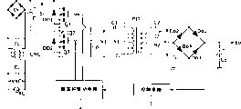
图1是图示了根据本发明第一实施例的开关电源电路的配置的电路图;1 is a circuit diagram illustrating the configuration of a switching power supply circuit according to a first embodiment of the present invention;
图2是图示了该实施例的开关电源电路中所包括的绝缘变换器变压器的一个配置示例的截面图;2 is a cross-sectional view illustrating one configuration example of an isolation converter transformer included in the switching power supply circuit of this embodiment;
图3A和图3B是图示了该实施例的电源电路中的主要部分的操作波形的波形图;3A and 3B are waveform diagrams illustrating operation waveforms of main parts in the power supply circuit of this embodiment;
图4是将该实施例的电源电路表示为电磁耦合谐振电路的等效电路图;Fig. 4 is the equivalent circuit diagram that represents the power supply circuit of this embodiment as an electromagnetic coupling resonant circuit;
图5是图示了该实施例的电源电路的恒压控制特性的示图;FIG. 5 is a diagram illustrating a constant voltage control characteristic of the power supply circuit of this embodiment;
图6是图示了作为该实施例的电源电路的恒压控制操作,用于应对AC输入电压变化和负载变化的开关频率控制范围(必要控制范围)的示图;6 is a diagram illustrating a switching frequency control range (necessary control range) for coping with AC input voltage variation and load variation as a constant voltage control operation of the power supply circuit of this embodiment;
图7是示出了该实施例的电源电路的作为负载的函数的AC到DC电源变换效率和开关频率特性的示图;7 is a graph showing AC-to-DC power conversion efficiency and switching frequency characteristics as a function of load of the power supply circuit of this embodiment;
图8是图示了根据本发明第二实施例的开关电源电路的配置的电路图;8 is a circuit diagram illustrating a configuration of a switching power supply circuit according to a second embodiment of the present invention;
图9是图示了根据本发明第三实施例的开关电源电路的配置的电路图;9 is a circuit diagram illustrating a configuration of a switching power supply circuit according to a third embodiment of the present invention;
图10是图示了根据本发明第四实施例的开关电源电路的配置的电路图;10 is a circuit diagram illustrating a configuration of a switching power supply circuit according to a fourth embodiment of the present invention;
图11是图示了根据本发明第五实施例的开关电源电路的配置的电路图;11 is a circuit diagram illustrating a configuration of a switching power supply circuit according to a fifth embodiment of the present invention;
图12是图示了含有传统复合谐振变换器的开关电源电路的一个配置示例的电路图;12 is a circuit diagram illustrating a configuration example of a switching power supply circuit including a conventional composite resonant converter;
图13是示出了图12中的电源电路的主要部分的操作波形的波形图;FIG. 13 is a waveform diagram showing operation waveforms of main parts of the power supply circuit in FIG. 12;
图14是示出了当初级侧和次级侧之间的耦合系数被设计为传统值时的恒压控制特性的示图;FIG. 14 is a graph showing constant voltage control characteristics when the coupling coefficient between the primary side and the secondary side is designed as a conventional value;
图15是图示了包括全波中心抽头整流电路作为其次级侧整流电路的图12中的电路的恒压控制特性的示图;以及FIG. 15 is a diagram illustrating constant voltage control characteristics of the circuit in FIG. 12 including a full-wave center-tapped rectification circuit as its secondary-side rectification circuit; and
图16是示出了图12中的电路的作为负载的函数的开关频率特性的特性图。FIG. 16 is a characteristic diagram showing switching frequency characteristics of the circuit in FIG. 12 as a function of load.
具体实施方式Detailed ways
下面将描述作为实现本发明的最佳实施方式(下文中也称作实施例)的开关电源电路。A switching power supply circuit will be described below as the best mode for realizing the present invention (hereinafter also referred to as an embodiment).
图1是图示了作为本发明第一实施例的开关电源电路的配置示例的电路图。FIG. 1 is a circuit diagram illustrating a configuration example of a switching power supply circuit as a first embodiment of the present invention.
图中所示的电源电路采用这样的配置作为其基本配置:其中通过半桥连接构成的他激电流谐振变换器与部分电压谐振电路相结合。The power supply circuit shown in the figure adopts as its basic configuration a configuration in which a separately excited current resonance converter constituted by half-bridge connection is combined with a partial voltage resonance circuit.
在该电源电路中,耦合到商用交流电源AC的是由滤波电容器CL和共模扼流圈CMC形成的共模噪声滤波器。In this power supply circuit, coupled to the commercial AC power supply AC is a common mode noise filter formed by a smoothing capacitor CL and a common mode choke coil CMC.
在噪声滤波器的下级,由桥式整流电路Di和平滑电容器Ci形成的全波整流和平滑电路被耦合到商用交流电源AC。In the lower stage of the noise filter, a full-wave rectification and smoothing circuit formed by a bridge rectification circuit Di and a smoothing capacitor Ci is coupled to a commercial AC power supply AC.
全波整流和平滑电路被馈送有来自商用交流电源AC的AC电压,并执行全波整流操作,从而在平滑电容器Ci两端获得经整流和平滑的电压Ei(DC输入电压)。经整流和平滑的电压Ei具有与AC输入电压VAC相同的电平。The full-wave rectification and smoothing circuit is fed with AC voltage from a commercial AC power supply AC, and performs a full-wave rectification operation, thereby obtaining a rectified and smoothed voltage Ei (DC input voltage) across the smoothing capacitor Ci. The rectified and smoothed voltage Ei has the same level as the AC input voltage VAC.
作为被馈送了DC输入电压并执行开关操作(间歇性)的电流谐振变换器,提供了开关电路,其中由MOS-FET形成的两个开关元件Q1和Q2通过半桥连接彼此连接,如图所示。阻尼二极管DD1和DD2分别与开关元件Q1和Q2的漏极与源极之间的沟道并联连接。阻尼二极管DD1的阳极和阴极分别连接到开关元件Q1的源极和漏极。类似地,阻尼二极管DD2的阳极和阴极分别连接到开关元件Q2的源极和漏极。阻尼二极管DD1和DD2分别是开关元件Q1和Q2所配备的体二极管。As a current resonant converter which is fed with a DC input voltage and performs switching operation (intermittently), there is provided a switching circuit in which two switching elements Q1 and Q2 formed of MOS-FETs are connected to each other by a half-bridge connection as shown in the figure Show. Damper diodes DD1 and DD2 are connected in parallel with the channels between the drains and sources of the switching elements Q1 and Q2, respectively. The anode and cathode of the damper diode DD1 are connected to the source and drain of the switching element Q1, respectively. Similarly, the anode and cathode of the damper diode DD2 are connected to the source and drain of the switching element Q2, respectively. Damper diodes DD1 and DD2 are body diodes provided with switching elements Q1 and Q2, respectively.
另外,初级侧部分谐振电容器Cp与开关元件Q2的漏极和源极之间的沟道并联连接。至少由初级侧部分谐振电容器Cp的电容和初级绕组N1的漏电感形成了部分谐振电路(部分电压谐振电路)。从而,实现了这样的部分电压谐振操作:其中仅当开关元件Q1和Q2被关断时,才出现电压谐振。In addition, the primary-side partial resonance capacitor Cp is connected in parallel with the channel between the drain and the source of the switching element Q2. A partial resonance circuit (partial voltage resonance circuit) is formed by at least the capacitance of the primary side partial resonance capacitor Cp and the leakage inductance of the primary winding N1. Thereby, a partial voltage resonance operation is realized in which voltage resonance occurs only when the switching elements Q1 and Q2 are turned off.
另外,振荡和驱动电路2被提供用于对开关元件Q1和Q2进行开关驱动。振荡和驱动电路2包括振荡电路和驱动电路,并且对其可以例如使用通用IC。振荡和驱动电路2中的振荡电路生成具有所需频率的振荡信号。驱动电路利用振荡信号来生成开关驱动信号,该开关驱动信号是用于对MOS-FET进行开关驱动的栅极电压,因此该开关驱动信号被施加到开关元件Q1和Q2的栅极。这样,根据基于开关驱动信号周期的开关频率,开关元件Q1和Q2实现了开关操作,使得它们以交替的定时被相继导通/关断。In addition, an oscillation and driving
绝缘变换器变压器PIT被提供以便将来自开关元件Q1和Q2的开关输出传递到次级侧。An isolated converter transformer PIT is provided to transfer switching outputs from the switching elements Q1 and Q2 to the secondary side.
绝缘变换器变压器PIT中的初级绕组N1的一端被串联连接到初级侧串联谐振电容器C1,并经由电容器C1被耦合到开关元件Q1的源极与开关元件Q2的漏极之间的连接节点(开关输出节点),其允许传递开关输出。初级绕组N1的另一端连接到初级侧的地。One end of the primary winding N1 in the insulating converter transformer PIT is connected in series to the primary-side series resonance capacitor C1, and is coupled to the connection node between the source of the switching element Q1 and the drain of the switching element Q2 (switching element Q2) via the capacitor C1. output node), which allows passing the switching output. The other end of the primary winding N1 is connected to the ground on the primary side.
绝缘变换器变压器PIT具有与图2的截面图所示的结构类似的结构。The isolated converter transformer PIT has a structure similar to that shown in the cross-sectional view of FIG. 2 .
如图2所示,绝缘变换器变压器PIT包括EE磁芯(EE形磁芯),其通过以磁芯柱互相面对的方式组合由铁氧体材料制成的E磁芯CR1和CR2而形成。As shown in FIG. 2, the insulating converter transformer PIT includes an EE core (EE-shaped core) formed by combining E cores CR1 and CR2 made of ferrite material in such a manner that the core legs face each other. .
此外,提供了线轴B,其由树脂等形成,并且具有这样的被分开的形状:初级侧和次级侧的缠绕部分彼此独立。初级侧绕组(初级绕组N1)缠绕在线轴B的一个缠绕部分上。次级侧绕组(次级绕组N2)缠绕在另一个缠绕部分上。已经如此缠绕了初级侧和次级侧绕组的线轴B被配合到EE磁芯(CR1,CR2),产生了这样的状态:其中在不同缠绕区域中的初级侧和次级侧绕组围绕EE磁芯的中心磁芯柱而缠绕。以这种方式,完成了绝缘变换器变压器PIT的整个结构。Further, there is provided the bobbin B, which is formed of resin or the like and has such a divided shape that the winding portions of the primary side and the secondary side are independent from each other. On one winding portion of the bobbin B, the primary side winding (primary winding N1 ) is wound. A secondary side winding (secondary winding N2) is wound on the other winding portion. The bobbin B, on which the primary side and secondary side windings have been thus wound, is fitted to the EE cores (CR1, CR2), resulting in a state in which the primary side and secondary side windings in different winding areas surround the EE core Wound around the center core leg. In this way, the entire structure of the isolated converter transformer PIT is completed.
在EE磁芯的中心磁芯柱中,如图所示,形成了间隙G。在该实施例中,间隙G被设计为例如具有约2.0mm的间隙长度,使得获得了初级侧与次级侧之间的弱耦合状态,其中它们之间的耦合系数k约为0.80或者更小。注意,当间隙长度被设置为大约2.0mm时,实际耦合系数k是0.735。可以通过将E磁芯CR1和CR2的中心磁芯柱设计为短于它们的两个外磁芯柱来形成间隙G。In the center leg of the EE core, a gap G is formed as shown. In this embodiment, the gap G is designed, for example, to have a gap length of about 2.0 mm, so that a weak coupling state between the primary side and the secondary side is obtained, wherein the coupling coefficient k between them is about 0.80 or less . Note that when the gap length is set to about 2.0 mm, the actual coupling coefficient k is 0.735. The gap G can be formed by designing the center legs of the E-cores CR1 and CR2 to be shorter than their two outer legs.
在以图12所示电源电路为典型的包含传统电流谐振变换器的电源电路中,如上所述,在绝缘变换器变压器PIT的磁芯中形成了大约1.0mm的间隙,从而获得了约0.8到0.9的耦合系数。In a power supply circuit including a conventional current resonant converter typified by the power supply circuit shown in FIG. A coupling factor of 0.9.
也就是说,在本发明中,绝缘变换器变压器PIT的初级侧与次级侧之间的耦合系数低于传统配置。That is, in the present invention, the coupling coefficient between the primary side and the secondary side of the isolated converter transformer PIT is lower than that of the conventional configuration.
返回参考图1,由于参考图2所描述的结构,绝缘变换器变压器PIT在初级绕组N1中产生一定的漏电感L1。另外,如上所述,初级绕组N1和初级侧串联谐振电容器C1串联连接。因此,初级绕组N1的漏电感L1与初级侧串联谐振电容器C1的电容形成了串联谐振电路(初级侧串联谐振电路)。Referring back to FIG. 1, due to the structure described with reference to FIG. 2, the isolated converter transformer PIT generates a certain leakage inductance L1 in the primary winding N1. In addition, as described above, the primary winding N1 and the primary side series resonance capacitor C1 are connected in series. Therefore, the leakage inductance L1 of the primary winding N1 and the capacitance of the primary side series resonance capacitor C1 form a series resonance circuit (primary side series resonance circuit).
初级侧串联谐振电路被连接到开关元件Q1和Q2的开关输出节点,因此来自开关元件Q1和Q2的开关输出被传递到初级侧串联谐振电路。初级侧串联谐振电路利用所传递的开关输出来执行谐振操作,其提供电流谐振操作作为初级侧开关变换器的操作。The primary side series resonant circuit is connected to the switching output nodes of the switching elements Q1 and Q2, and thus the switching outputs from the switching elements Q1 and Q2 are delivered to the primary side series resonant circuit. The primary side series resonant circuit utilizes the passed switching output to perform resonant operation, which provides current resonant operation as the operation of the primary side switching converter.
根据上述说明,图1所示的初级侧开关变换器通过初级侧串联谐振电路(L1-C1)提供了电流谐振操作,并通过上述初级侧部分电压谐振电路(Cp//L1)提供了部分电压谐振操作。According to the above description, the primary side switching converter shown in Figure 1 provides current resonant operation through the primary side series resonant circuit (L1-C1) and partial voltage through the above primary side partial voltage resonant circuit (Cp//L1) Resonant operation.
也就是说,图中所示的电源电路的初级侧采用这样的配置:其中提供作为初级侧开关变换器的谐振变换器的谐振电路被与另一谐振电路相结合。在本说明书中,由这样结合的两个谐振电路形成的开关变换器也被称作复合谐振变换器。That is, the primary side of the power supply circuit shown in the figure adopts a configuration in which a resonance circuit provided as a resonance converter of a primary-side switching converter is combined with another resonance circuit. In this specification, a switching converter formed by such combined two resonant circuits is also referred to as a composite resonant converter.
在绝缘变换器变压器PIT的次级绕组N2中,激励(感应)了依赖于被传递到初级绕组N1的开关输出的交变电压。In the secondary winding N2 of the insulating converter transformer PIT, an alternating voltage depending on the switching output delivered to the primary winding N1 is excited (induced).
假设次级绕组N2是由包含整流二极管Do1到Do4的桥式整流电路以及平滑电容器Co形成的全波桥式整流电路。Assume that the secondary winding N2 is a full-wave bridge rectification circuit formed by a bridge rectification circuit including rectification diodes Do1 to Do4 and a smoothing capacitor Co.
此外,在本实施例中,次级侧串联谐振电容器C2与次级绕组N2串联连接在全波桥式整流电路中。因此,由于次级侧串联谐振电容器C2的电容和次级绕组N2的漏电感L2,在绝缘变换器变压器PIT的次级侧上也形成了串联谐振电路。Furthermore, in the present embodiment, the secondary-side series resonance capacitor C2 is connected in series with the secondary winding N2 in the full-wave bridge rectifier circuit. Therefore, a series resonance circuit is also formed on the secondary side of the insulating converter transformer PIT due to the capacitance of the secondary side series resonance capacitor C2 and the leakage inductance L2 of the secondary winding N2.
次级侧的具体配置如下。次级绕组N2的一端串联连接到次级侧串联谐振电容器C2,并经由电容器C2,耦合到整流二极管Do1的阳极与整流二极管Do2的阴极之间的连接节点。次级绕组N2的另一端耦合到整流二极管Do3的阳极与整流二极管Do4的阴极之间的连接节点。The specific configuration of the secondary side is as follows. One end of the secondary winding N2 is connected in series to the secondary side series resonant capacitor C2, and is coupled to a connection node between the anode of the rectifier diode Do1 and the cathode of the rectifier diode Do2 via the capacitor C2. The other end of the secondary winding N2 is coupled to the connection node between the anode of the rectifier diode Do3 and the cathode of the rectifier diode Do4.
整流二极管Do2的阳极与整流二极管Do4的阳极之间的连接节点被连接到次级侧的地。整流二极管Do1的阴极与整流二极管Do3的阴极之间的连接节点被连接到平滑电容器Co的正电极。平滑电容器Co的负电极被连接到次级侧的地。A connection node between the anode of the rectifier diode Do2 and the anode of the rectifier diode Do4 is connected to the ground on the secondary side. The connection node between the cathode of the rectification diode Do1 and the cathode of the rectification diode Do3 is connected to the positive electrode of the smoothing capacitor Co. The negative electrode of the smoothing capacitor Co is connected to the ground on the secondary side.
根据该连接结构,在次级绕组N2中出现的交变电压的一半周期的时段中,一对整流二极管Do1和Do4实现整流操作,从而对平滑电容器Co充电。而在次级绕组N2中出现的交变电压的另一半周期的时段中,一对整流二极管Do2和Do3的整流操作对平滑电容器Co充电。According to this connection structure, the pair of rectifying diodes Do1 and Do4 perform a rectifying operation during a period of a half cycle of the alternating voltage appearing in the secondary winding N2, thereby charging the smoothing capacitor Co. While during the period of the other half cycle of the alternating voltage appearing in the secondary winding N2, the rectifying operation of the pair of rectifying diodes Do2 and Do3 charges the smoothing capacitor Co.
由于这些整流二极管Do1到Do4的全波整流操作,在平滑电容器Co两端获得了次级侧DC输出电压Eo,其依赖于次级绕组N2中激励的交变电压的电平。次级侧DC输出电压Eo被提供给负载(未示出),并且被分路并输入到后面将描述的控制电路1作为检出电压。Due to the full-wave rectification operation of these rectifying diodes Do1 to Do4, a secondary side DC output voltage Eo is obtained across the smoothing capacitor Co, which depends on the level of the alternating voltage excited in the secondary winding N2. The secondary-side DC output voltage Eo is supplied to a load (not shown), and is branched and input to a
在该配置中,次级侧上所形成的串联谐振电路通过整流二极管Do1到Do4提供了电流谐振操作,作为次级侧整流操作。In this configuration, the series resonance circuit formed on the secondary side provides a current resonance operation as a secondary side rectification operation through the rectification diodes Do1 to Do4.
控制电路1向振荡和驱动电路2提供检测输出,该检测输入依赖于次级侧DC输出电压Eo的电平变化。振荡和驱动电路2驱动并控制开关元件Q1和Q2,使得开关频率根据从控制电路1输入的检测输出而改变。为此,振荡和驱动电路2改变由其中的振荡电路生成的振荡信号的频率。The
由于开关元件Q1和Q2的开关频率被改变,所以初级侧串联谐振电路的谐振阻抗改变,因此从绝缘变换器变压器PIT的初级侧传递到次级侧的功率量改变了。从而,允许用于稳定次级侧DC输出电压Eo电平的操作。Since the switching frequency of the switching elements Q1 and Q2 is changed, the resonance impedance of the primary side series resonance circuit changes, and thus the amount of power transferred from the primary side to the secondary side of the insulating converter transformer PIT changes. Thus, an operation for stabilizing the level of the secondary-side DC output voltage Eo is allowed.
在本实施例的电源电路所使用的开关频率控制方法中,采用了比初级侧串联谐振电路的谐振频率fo1高的频率范围作为开关频率的可变范围。即,采用了所谓的上侧控制方法。In the switching frequency control method used in the power supply circuit of this embodiment, a frequency range higher than the resonant frequency fo1 of the primary-side series resonant circuit is adopted as the variable range of the switching frequency. That is, a so-called upper side control method is adopted.
一般,当频率是谐振频率时,串联谐振电路的谐振阻抗变为最低。因此,如果与本实施例类似地采用了基于串联谐振电路谐振频率的上侧控制方法,则越高的开关频率fs导致越高的谐振阻抗。Generally, when the frequency is the resonance frequency, the resonance impedance of the series resonance circuit becomes lowest. Therefore, if the upper side control method based on the resonant frequency of the series resonant circuit is adopted similarly to the present embodiment, a higher switching frequency fs leads to a higher resonant impedance.
因此,例如如果有朝向较大负载的趋势,并且次级侧DC输出电压Eo从而降低时,执行降低开关频率的控制。开关频率的降低造成谐振阻抗降低,谐振阻抗的降低增加了从初级侧传递到次级侧的功率量,从而提高了次级侧DC输出电压Eo。Therefore, for example, if there is a tendency toward a larger load, and the secondary-side DC output voltage Eo thereby decreases, control to decrease the switching frequency is performed. The reduction of the switching frequency results in a reduction of the resonance impedance, which increases the amount of power transferred from the primary side to the secondary side, thereby increasing the secondary side DC output voltage Eo.
相反,当出现朝向较小负载的趋势,并且次级侧DC输出电压Eo从而升高时,执行增大开关频率的控制。从而,谐振阻抗被提高,因此功率传递量被降低,这降低了次级侧DC输出电压Eo。以这种方式,开关频率的变化可以稳定次级侧DC输出电压Eo。Conversely, when a tendency toward a smaller load occurs, and the secondary-side DC output voltage Eo rises thereby, control to increase the switching frequency is performed. Consequently, the resonance impedance is increased, and thus the power transfer amount is reduced, which lowers the secondary-side DC output voltage Eo. In this way, the variation of the switching frequency can stabilize the secondary side DC output voltage Eo.
图1的电源电路采用了适应宽范围的配置,其可以适应于利用AC 100V系统和AC 200V系统两者而工作。The power supply circuit of FIG. 1 adopts a wide-range-adaptive configuration, which can be adapted to work with both the
在图1的电源电路中,如上所述,在初级侧和次级侧上都提供了串联谐振电路,并且绝缘变换器变压器PIT中的耦合系数k被设置为低于传统系数值。In the power supply circuit of FIG. 1, as described above, the series resonance circuit is provided on both the primary side and the secondary side, and the coupling coefficient k in the insulating converter transformer PIT is set to be lower than the conventional coefficient value.
这样的配置提供了适应宽范围的电路。下面将参考图4到图6来描述这一点。Such a configuration provides a circuit suitable for a wide range. This will be described below with reference to FIGS. 4 to 6 .
图4的电路图在初级侧串联谐振电路和次级侧串联谐振电路之间关系的方面,示出了图1中的本实施例的电源电路的等效电路。该等效电路图中与图1所示相同的部分被赋予相同的标号。The circuit diagram of FIG. 4 shows an equivalent circuit of the power supply circuit of the present embodiment in FIG. 1 in terms of the relationship between the primary side series resonance circuit and the secondary side series resonance circuit. In this equivalent circuit diagram, the same parts as those shown in FIG. 1 are given the same reference numerals.
图4图示了这样的绝缘变换器变压器PIT:围绕其缠绕了具有某个匝数比1∶n的初级绕组N1和次级绕组N2。在该图中,绝缘变换器变压器PIT的初级侧和次级侧之间的耦合程度由耦合系数k表示。FIG. 4 illustrates an isolated converter transformer PIT around which a primary winding N1 and a secondary winding N2 having a certain turns ratio 1:n are wound. In this figure, the degree of coupling between the primary side and the secondary side of the insulating converter transformer PIT is represented by a coupling coefficient k.
在绝缘变换器变压器PIT的初级侧上,L11和L1e分别代表初级绕组N1的漏电感和磁化电感。另外,绝缘变换器变压器PIT的次级侧上的L21和L2e分别代表次级绕组N2的漏电感和磁化电感。On the primary side of the insulating converter transformer PIT, L11 and L1e represent the leakage inductance and the magnetizing inductance of the primary winding N1, respectively. In addition, L21 and L2e on the secondary side of the insulating converter transformer PIT represent leakage inductance and magnetizing inductance of the secondary winding N2, respectively.
在图4的等效电路图中,具有开关频率fs的AC电压(频率信号)被输入到绝缘变换器变压器PIT的初级侧。即,该输入电压是来自初级侧开关变换器(开关元件Q1和Q2)的开关输出。In the equivalent circuit diagram of FIG. 4, an AC voltage (frequency signal) having a switching frequency fs is input to the primary side of the insulating converter transformer PIT. That is, the input voltage is the switching output from the primary side switching converter (switching elements Q1 and Q2).
在绝缘变换器变压器PIT的初级侧上,具有开关频率fs的输入AC电压被提供到初级侧串联谐振电路。如图所示,该初级侧串联谐振电路可以被认为是这样的电路:其中初级侧串联谐振电容器C1与漏电感L11串联连接到初级绕组N1,并且磁化电感L1e与初级绕组N1并联连接。On the primary side of the insulating converter transformer PIT, an input AC voltage with a switching frequency fs is supplied to the primary side series resonant circuit. As shown, the primary side series resonance circuit can be regarded as a circuit in which the primary side series resonance capacitor C1 is connected in series with the leakage inductance L11 to the primary winding N1, and the magnetizing inductance L1e is connected in parallel with the primary winding N1.
类似地,绝缘变换器变压器PIT的次级侧串联谐振电路可以被认为是这样的电路:其中次级侧串联谐振电容器C2与漏电感L2l串联连接到次级绕组N2,并且磁化电感L2e与次级绕组N2并联连接。另外,在该图中,来自具有上述配置的次级侧串联谐振电路的输出被提供到负载RL。负载RL对应于在次级侧全波整流电路之后的电路和负载。Similarly, the secondary side series resonant circuit of the isolated converter transformer PIT can be considered as a circuit in which the secondary side series resonant capacitor C2 is connected in series with the leakage inductance L2l to the secondary winding N2, and the magnetizing inductance L2e is connected to the secondary Winding N2 is connected in parallel. Also, in this figure, the output from the secondary-side series resonance circuit having the above configuration is supplied to the load RL. The load RL corresponds to the circuit and the load after the secondary-side full-wave rectification circuit.
在具有上述连接配置的图4的等效电路中,初级绕组N1的漏电感L11可以由公式1表示,其中k是绝缘变换器变压器PIT的耦合系数,L1是初级绕组N1的自感。In the equivalent circuit of FIG. 4 with the above connection configuration, the leakage inductance L11 of the primary winding N1 can be expressed by
L11=(1-k2)L1 ……公式1L11=(1-k 2 )L1...
初级绕组N1的磁化电感L1e可以由公式2表示。The magnetizing inductance L1e of the primary winding N1 can be expressed by
L1e=k2×L1 ……公式2L1e=k 2 ×L1...
类似地,次级绕组N2的漏电感L2l和磁化电感L2e可以分别由公式3和公式4表示,其中L2是次级绕组N2的自感。Similarly, the leakage inductance L2l and the magnetizing inductance L2e of the secondary winding N2 can be expressed by Equation 3 and Equation 4, respectively, where L2 is the self-inductance of the secondary winding N2.
L2l=(1-k2)L2 ……公式3L2l=(1-k 2 )L2 ... Formula 3
L2e=k2×L2 ……公式4L2e=k 2 ×L2 ......Formula 4
图4的等效电路包括初级侧上的初级侧串联谐振电路和次级侧上的次级侧串联谐振电路,其间具有绝缘变换器变压器PIT的电磁感应的媒介。因此,该图的电路可以被认为是采用电磁耦合的耦合谐振电路。因此,图1的电源电路的关于次级侧DC输出电压Eo的恒压控制特性依赖于绝缘变换器变压器PIT的耦合程度(耦合系数k)而不同。下面将参考图5描述这一点。The equivalent circuit of FIG. 4 includes a primary-side series resonance circuit on the primary side and a secondary-side series resonance circuit on the secondary side with an intermediary of electromagnetic induction of the insulating converter transformer PIT in between. Therefore, the circuit of this figure can be considered as a coupled resonant circuit using electromagnetic coupling. Therefore, the constant voltage control characteristics of the power supply circuit of FIG. 1 with respect to the secondary side DC output voltage Eo differ depending on the degree of coupling (coupling coefficient k) of the insulating converter transformer PIT. This will be described below with reference to FIG. 5 .
图5示出了图4的等效电路的相对于对其的输入(开关频率信号)的输出特性。具体地说,次级侧DC输出电压Eo的控制特性被表示为电压Eo与开关频率fs之间的关系。FIG. 5 shows output characteristics of the equivalent circuit of FIG. 4 with respect to an input thereto (switching frequency signal). Specifically, the control characteristic of the secondary-side DC output voltage Eo is expressed as a relationship between the voltage Eo and the switching frequency fs.
在图5中,开关频率绘制在横坐标上,而次级侧DC输出电压Eo的电平绘制在纵坐标上。In FIG. 5 , the switching frequency is plotted on the abscissa, and the level of the secondary-side DC output voltage Eo is plotted on the ordinate.
在横坐标上,初级侧串联谐振电路的谐振频率fo1和次级侧串联谐振电路的谐振频率fo2彼此重叠,这意味着不管谐振频率fo1和fo2的设定值如何,都获得了类似的特性。On the abscissa, the resonance frequency fo1 of the primary side series resonance circuit and the resonance frequency fo2 of the secondary side series resonance circuit overlap each other, which means that similar characteristics are obtained regardless of the set values of the resonance frequencies fo1 and fo2.
当绝缘变换器变压器PIT采用耦合系数k为1的强耦合时,由于公式1和公式3中的k被1替换,初级绕组N1的漏电感L1l和次级绕组N2的漏电感L2l由公式5表示。When the isolated converter transformer PIT adopts a strong coupling with a coupling coefficient k of 1, since k in
L11=L2l=0 ……公式5L11=L2l=0 ...
即,当绝缘变换器变压器PIT采用强耦合时,在初级绕组N1和次级绕组N2中不存在漏电感。That is, when the isolated converter transformer PIT adopts strong coupling, there is no leakage inductance in the primary winding N1 and the secondary winding N2.
当绝缘变换器变压器PIT的初级侧和次级侧这样被强耦合时,恒压控制特性绘制出如图5的特性曲线1所示的所谓的双峰曲线。在该曲线中,当开关频率分别位于与初级侧和次级侧串联谐振电路的谐振频率fo1和fo2不同的频率值f1和f2处时,次级侧DC输出电压Eo变为峰值。When the primary side and the secondary side of the insulating converter transformer PIT are thus strongly coupled, the constant voltage control characteristic draws a so-called double-peak curve as shown in
频率f1由等式1表示。Frequency f1 is represented by
频率f2由等式2表示。Frequency f2 is represented by
在等式1和等式2中,作为其中一项的fo代表中心谐振频率,其存在于初级侧串联谐振电路的谐振频率fo1与次级侧串联谐振电路的谐振频率fo2之间的中心处。中心谐振频率的确定依赖于初级侧的阻抗、次级侧的阻抗以及初级侧和次级侧共有的阻抗(互耦合电感M)。In
互耦合电感M由等式3表示。The mutual coupling inductance M is represented by Equation 3.
如果耦合系数k逐渐从1降低(例如,如果耦合状态逐渐从强耦合朝向弱耦合移动),则在图5的特性曲线1中出现这样的变化:双峰趋势逐渐减弱,并且接近中心谐振频率fo的曲线变得平坦。接着,当耦合系数k降低到某个值时,耦合状态达到所谓的临界耦合状态。在临界耦合状态中,如特性曲线2所示,双峰特性趋势已经消失,并且在中心谐振频率fo附近的曲线的形状是平坦的。If the coupling coefficient k gradually decreases from 1 (for example, if the coupling state gradually moves from strong coupling to weak coupling), such a change occurs in
如果耦合系数k从临界耦合状态进一步降低,从而进一步向弱耦合状态发展,则获得了如图5的特性曲线3所示的单峰特性,其中仅在中心频率fo处存在一个峰值。特性曲线3与特性曲线1和2的比较清楚显示出,虽然特性曲线3自身的峰值水平低于特性曲线1和2的峰值水平,但是特性曲线3的二次曲线形状具有比特性曲线1和2更陡的斜度。If the coupling coefficient k is further reduced from the critical coupling state, thereby further developing to the weak coupling state, then a single-peak characteristic as shown in characteristic curve 3 of Fig. 5 is obtained, in which there is only one peak at the center frequency fo. A comparison of characteristic curve 3 with
本实施例的绝缘变换器变压器PIT采用弱耦合状态,其中耦合系数k小于约0.8。这样的耦合系数k提供了基于由特性曲线3所示的单峰特性的操作。The isolated converter transformer PIT of this embodiment adopts a weak coupling state, wherein the coupling coefficient k is less than about 0.8. Such a coupling coefficient k provides an operation based on the unimodal characteristic shown by characteristic curve 3 .
当图5所示的单峰特性与传统复合谐振变换器的图14中的恒压控制特性相比较时,可以清楚看到图14中的特性的二次曲线示出了比图5的曲线缓和得多的斜度。When the unimodal characteristic shown in Fig. 5 is compared with the constant voltage control characteristic in Fig. 14 of the conventional composite resonant converter, it can be clearly seen that the quadratic curve of the characteristic in Fig. 14 shows a gentler curve than that in Fig. 5 Much more slope.
由于传统电源电路的特性示出了如图14所示的缓和曲线,所以即使当电路例如具有适应单范围的配置时,用于对次级侧DC输出电压Eo的恒压控制的开关频率fs的必要控制范围也是从约80kHz到约200kHz,因此Δfs约是100kHz或更大。Since the characteristics of the conventional power supply circuit show a relaxation curve as shown in FIG. The necessary control range is also from about 80 kHz to about 200 kHz, so Δfs is about 100 kHz or more.
因此,如上所述,仅通过开关频率控制来实现恒压控制,很难提供具有适应宽范围的特性的电源电路。Therefore, as described above, it is difficult to provide a power supply circuit having characteristics suitable for a wide range by only realizing constant voltage control by switching frequency control.
相反,本实施例的恒压控制特性是图5的特性曲线3所示的单峰特性,因此其恒压控制操作由图6的特性曲线表述。In contrast, the constant voltage control characteristic of the present embodiment is a single-peak characteristic shown by the characteristic curve 3 of FIG. 5, so its constant voltage control operation is expressed by the characteristic curve of FIG.
图6图示了从根据本实施例的图1的电源电路得到的四条特性曲线A到D。特性曲线A和B分别对应于当AC输入电压VAC为100V(AC100V系统)时的最大负载功率Pomax和最小负载功率Pomin。特性曲线C和D分别对应于当AC输入电压VAC为230V(AC 200V系统)时的最大负载功率Pomax和最小负载功率Pomin。FIG. 6 illustrates four characteristic curves A to D obtained from the power supply circuit of FIG. 1 according to the present embodiment. The characteristic curves A and B respectively correspond to the maximum load power Pomax and the minimum load power Pomin when the AC input voltage VAC is 100V (AC100V system). Characteristic curves C and D respectively correspond to the maximum load power Pomax and the minimum load power Pomin when the AC input voltage VAC is 230V (AC 200V system).
如从图6清楚看到的,当AC输入电压VAC是100V(对应于AC100V系统输入)时,将次级侧DC输出电压Eo恒定地保持在所需电平tg处所需的开关频率的可变控制范围(必要控制范围)由Δfs1表示。具体地说,必要控制范围是从在特性曲线A上提供了电平tg的开关频率fs到在特性曲线B上提供了电平tg的开关频率fs的频率范围。As clearly seen from Fig. 6, when the AC input voltage VAC is 100V (corresponding to AC100V system input), the possibility of the switching frequency required to keep the secondary side DC output voltage Eo constant at the desired level tg The variable control range (necessary control range) is represented by Δfs1. Specifically, the necessary control range is a frequency range from the switching frequency fs at which the level tg is provided on the characteristic curve A to the switching frequency fs at which the level tg is provided on the characteristic curve B.
另外,当AC输入电压VAC是230V(对应于AC 200V系统输入)时,将次级侧DC输出电压Eo恒定地保持在所需电平tg处所需的开关频率的可变控制范围(必要控制范围)由Δfs2表示。具体地说,必要控制范围是从在特性曲线C上提供了电平tg的开关频率fs到在特性曲线D上提供了电平tg的开关频率fs的频率范围。Also, when the AC input voltage VAC is 230V (corresponding to the AC 200V system input), the variable control range of the switching frequency required to keep the secondary side DC output voltage Eo constant at the desired level tg (necessary control range) is represented by Δfs2. Specifically, the necessary control range is a frequency range from the switching frequency fs at which the level tg is provided on the characteristic curve C to the switching frequency fs at which the level tg is provided on the characteristic curve D.
如上所述,与图14所示的控制特性相比,本实施例作为次级侧DC输出电压Eo控制特性的单峰特性绘制出了相当陡的二次曲线。As described above, the present embodiment draws a considerably steeper quadratic curve as the single-peak characteristic of the control characteristic of the secondary-side DC output voltage Eo compared with the control characteristic shown in FIG. 14 .
因此,当AC输入电压VAC分别是100V和230V时所获得的必要控制范围Δfs1和Δfs2比图14中的范围Δfs小得多。例如,实际测量的范围Δfs1和Δfs2被发现是图14中的实际范围Δfs的大约十分之一。Therefore, the necessary control ranges Δfs1 and Δfs2 obtained when the AC input voltages VAC are 100 V and 230 V, respectively, are much smaller than the range Δfs in FIG. 14 . For example, the actually measured ranges Δfs1 and Δfs2 were found to be approximately one-tenth of the actual range Δfs in FIG. 14 .
另外,范围Δfs1中的最小开关频率(在特性曲线A上提供了电平tg的开关频率fs)与范围Δfs2中的最大开关频率(在特性曲线D上提供了电平tg的开关频率fs)之间的频率可变范围(ΔfsA)也相当小。In addition, the difference between the minimum switching frequency in the range Δfs1 (the switching frequency fs that provides the level tg on the characteristic curve A) and the maximum switching frequency in the range Δfs2 (the switching frequency fs that provides the level tg on the characteristic curve D) The frequency variable range (ΔfsA) between them is also quite small.
图1中本实施例的电源电路的实际频率可变范围ΔfsA充分地落入目前的开关驱动IC(振荡和驱动电路2)的开关频率可变范围之内。也就是说,图1的电源电路可以实际地在频率可变范围ΔfsA之内可变地控制其开关频率。该事实意味着图1的电源电路对于AC 100V系统和AC 200V系统两者的商用AC电压输入都可以稳定次级侧DC输出电压Eo。也就是说,图1的电源电路允许仅通过开关频率控制就具有适应宽范围的配置。The actual frequency variable range ΔfsA of the power supply circuit of this embodiment in FIG. 1 falls well within the switching frequency variable range of the current switch drive IC (oscillation and drive circuit 2 ). That is to say, the power supply circuit of FIG. 1 can actually variably control its switching frequency within the frequency variable range ΔfsA. This fact means that the power supply circuit of Fig. 1 can stabilize the secondary side DC output voltage Eo for commercial AC voltage input of both
注意,作为通信技术中用于扩大由晶体管形成的放大电路的放大带宽的单元,采用电磁耦合的耦合谐振电路是公知的。例如,该单元的典型示例是中频变换放大器。在该技术领域中,并没有使用由弱耦合造成的单峰特性,而是使用了由强耦合造成的双峰特性或者临界耦合造成的平坦特性。在本实施例中,关于采用电磁耦合的这种耦合谐振电路的技术,在通信技术领域中还没有被使用过的由弱耦合造成的单峰特性被有利地使用在谐振开关变换器的领域中。因此,如上所述,稳定次级侧DC输出电压Eo所需的开关频率可变范围(必要控制范围)被缩窄,这使得仅通过根据开关频率控制的恒压控制,就可以允许适应宽范围的配置。Note that, as a unit for expanding the amplification bandwidth of an amplification circuit formed of transistors in communication technology, a coupled resonance circuit using electromagnetic coupling is known. For example, a typical example of this unit is an intermediate frequency conversion amplifier. In this technical field, instead of single-peak characteristics due to weak coupling, double-peak characteristics due to strong coupling or flat characteristics due to critical coupling are used. In the present embodiment, with regard to the technique of such coupled resonant circuits using electromagnetic coupling, the single-peak characteristic caused by weak coupling, which has not been used in the field of communication technology, is advantageously used in the field of resonant switching converters . Therefore, as described above, the switching frequency variable range (necessary control range) required to stabilize the secondary side DC output voltage Eo is narrowed, which allows adaptation to a wide range only by constant voltage control according to switching frequency control Configuration.
一般而言,当弱耦合的程度在绝缘变换器变压器PIT的初级侧与次级侧之间加大时,出现了这样的趋势:绝缘变换器变压器PIT中的功率损耗被增大,因此电源变换效率被相应地降低。但是,如后面所描述的,本实施例可以获得对于实际使用来说足够的电源变换效率。这是由于在次级侧上也形成了串联谐振电路(次级侧串联谐振电路)的特性。In general, when the degree of weak coupling is increased between the primary side and the secondary side of the isolating converter transformer PIT, there is a tendency that the power loss in the isolating converter transformer PIT is increased, so that the power conversion Efficiency is reduced accordingly. However, as described later, the present embodiment can obtain power conversion efficiency sufficient for practical use. This is due to the characteristics of a series resonance circuit (secondary side series resonance circuit) formed also on the secondary side.
具体地说,提供次级侧串联谐振电路使得增加了其谐振操作所引起的能量,含有所增加的能量的功率可以被提供为次级侧DC输出电压Eo。因此,由于弱耦合而降低的效率被补偿了。Specifically, the secondary side series resonance circuit is provided such that the energy caused by its resonance operation is increased, and power containing the increased energy can be supplied as the secondary side DC output voltage Eo. Therefore, the reduced efficiency due to weak coupling is compensated.
应当注意,需要再次确认,当与本实施例类似地提供了次级侧串联谐振电容器C2以在次级侧上也形成串联谐振电路时,在每个半周期时段中,绕组电流都需要流过整个次级绕组N2,以便提供谐振操作作为次级侧整流操作。因此,次级侧上的整流电路必须具有除了半波整流电路和全波中心抽头整流电路之外的电路配置。相应地,图1的电源电路包括全波桥式整流电路作为其次级侧整流电路。It should be noted that it needs to be reconfirmed that when the secondary side series resonant capacitor C2 is provided similarly to this embodiment to also form a series resonant circuit on the secondary side, in each half cycle period, the winding current needs to flow through entire secondary winding N2 in order to provide resonant operation as secondary side rectified operation. Therefore, the rectification circuit on the secondary side must have a circuit configuration other than the half-wave rectification circuit and the full-wave center-tapped rectification circuit. Correspondingly, the power supply circuit of FIG. 1 includes a full-wave bridge rectification circuit as its secondary side rectification circuit.
对于这种情形,当打算采用该实施例的适应宽范围的配置时,与图12所示类似的传统全波中心抽头整流电流并没有被用作次级侧整流电路。因此,不存在这样的可能:全波中心抽头整流器的使用阻止了采用开关频率控制来实现适应宽范围的配置。For this case, when the wide-ranging configuration of this embodiment is intended, a conventional full-wave center-tap rectification current similar to that shown in FIG. 12 is not used as a secondary-side rectification circuit. Therefore, there is no possibility that the use of a full-wave center-tapped rectifier prevents the use of switching frequency control to accommodate a wide range of configurations.
图3A和图3B是用于示出图1的电源电路中的主要部分的操作的波形图。3A and 3B are waveform diagrams for illustrating operations of main parts in the power supply circuit of FIG. 1 .
图3A示出了当AC输入电压VAC是100V时的操作波形。图3B示出了当AC输入电压VAC是230V时的操作波形。此外,在图3A和图3B两者中,左边和右边的图分别示出了当负载功率Po为200W和0W时的操作波形。FIG. 3A shows operation waveforms when the AC input voltage VAC is 100V. FIG. 3B shows operation waveforms when the AC input voltage VAC is 230V. In addition, in both FIGS. 3A and 3B , the left and right graphs show operation waveforms when the load power Po is 200W and 0W, respectively.
在该实施例的电源电路中,200W和0W的负载功率Po分别对应于最大负载功率(Pomax)和最小负载功率(Pomin)。In the power supply circuit of this embodiment, the load powers Po of 200 W and 0 W correspond to the maximum load power (Pomax) and the minimum load power (Pomin), respectively.
图3A和图3B中的实验结果是当具有下列特性的元件被选择作为图1的电路的主要部分时而得到的The experimental results in Figure 3A and Figure 3B are obtained when components having the following characteristics are selected as the main part of the circuit of Figure 1
·绝缘变换器变压器PIT具有间隙长度2.0mm的间隙G和约0.735的耦合系数k;匝数为30T的初级绕组N1;匝数为26T的次级绕组N2The isolated converter transformer PIT has a gap G with a gap length of 2.0 mm and a coupling coefficient k of about 0.735; a primary winding N1 with a number of turns of 30T; a secondary winding N2 with a number of turns of 26T
·初级侧串联谐振电容器C1的电容为0.039μFThe capacitance of the primary side series resonant capacitor C1 is 0.039μF
·次级侧串联谐振电容器C2的电容为0.027μF。• The capacitance of the secondary side series resonant capacitor C2 is 0.027 μF.
通过这样设置初级和次级绕组N1和N2的匝数以及初级侧和次级侧串联谐振电容器C1和C2的电容,初级侧串联谐振电路的谐振频率fo1和次级侧串联谐振电路的谐振频率fo2被分别设置为约60kHz和约84kHz。By thus setting the number of turns of the primary and secondary windings N1 and N2 and the capacitances of the primary side and secondary side series resonance capacitors C1 and C2, the resonance frequency fo1 of the primary side series resonance circuit and the resonance frequency fo2 of the secondary side series resonance circuit are set to approximately 60kHz and approximately 84kHz, respectively.
另外,通过选择上述各个元件,次级绕组N2每匝的感应电压电平被设置为5V/T。In addition, the induced voltage level per turn of the secondary winding N2 is set to 5V/T by selecting the above-mentioned respective components.
参考图3A和图3B,矩形波电压V1是开关元件Q2两端的电压,指示开关元件Q2的导通/关断定时。电压V1具有这样的波形:其中在开关元件Q2处于导通状态的导通时段中,电压电平处于0电平,并且在开关元件Q2处于关断状态的关断时段中,电压电平被箝位在经整流和平滑的电压Ei的电平。Referring to FIGS. 3A and 3B , the rectangular wave voltage V1 is a voltage across the switching element Q2 indicating the on/off timing of the switching element Q2 . The voltage V1 has a waveform in which the voltage level is at 0 level in the conduction period when the switching element Q2 is in the conduction state, and the voltage level is clamped in the off period in which the switching element Q2 is in the off state. bit at the level of the rectified and smoothed voltage Ei.
在开关元件Q2的导通时段期间,具有所示波形的开关电流IQ2流过由开关元件Q2和箝位二极管DD2组成的开关电路系统。而在开关元件Q2的关断时段期间,开关电流IQ2处于0水平。During the conduction period of the switching element Q2, a switching current IQ2 having the waveform shown flows through the switching circuitry composed of the switching element Q2 and the clamp diode DD2. Whereas, during the off period of the switching element Q2, the switching current IQ2 is at 0 level.
另外,虽然未被图示出,但是开关元件Q1两端的电压和流过另一开关电路系统(Q1,DD1)的开关电流具有这样的波形:该波形通过分别将电压V1和开关电流IQ2的波形的相位移动180°而得到。即,开关元件Q1和Q2以相同的周期实现了开关操作,使得它们被交替地导通/关断。In addition, although not shown, the voltage across the switching element Q1 and the switching current flowing through the other switching circuitry (Q1, DD1) have waveforms that are obtained by respectively combining the voltage V1 and the switching current IQ2 is obtained by shifting the phase of 180°. That is, the switching elements Q1 and Q2 perform switching operations with the same period so that they are alternately turned on/off.
初级侧串联谐振电流Io(未示出)流过初级侧串联谐振电路(L1-C1),作为从流过这些开关电路(Q1,DD1)和(Q2,DD2)的开关电流的合成而得到的电流分量。The primary side series resonant current Io (not shown) flows through the primary side series resonant circuit (L1-C1) as a result of the synthesis of the switching currents flowing through these switching circuits (Q1, DD1) and (Q2, DD2) current component.
参考图3A,当AC输入电压VAC是100V时,开关电流IQ2的峰值水平在负载功率是200W的最大负载功率Pomax和0W的最小负载功率Pomin时分别为约6.0安培和约3.5安培。Referring to FIG. 3A , when the AC input voltage VAC is 100V, the peak levels of the switching current IQ2 are about 6.0 A and about 3.5 A when the load power is the maximum load power Pomax of 200W and the minimum load power Pomin of 0W, respectively.
参考图3B,当AC输入电压VAC是230V时,开关电流IQ2的峰值水平在负载功率是200W的最大负载功率Pomax和0W的最小负载功率Pomin时分别为约2.6安培和约2.4安培。Referring to FIG. 3B , when the AC input voltage VAC is 230V, the peak levels of the switching current IQ2 are about 2.6 A and about 2.4 A when the load power is the maximum load power Pomax of 200W and the minimum load power Pomin of 0W, respectively.
由上述电压V1和开关电流IQ2指示的初级侧上的操作在绝缘变换器变压器PIT的次级绕组N2中感应了具有所示波形的交变电压V2。交变电压V2具有这样的波形:其中电压电平被箝位在次级侧DC输出电压Eo的电平处。The operation on the primary side indicated by the aforementioned voltage V1 and switching current IQ2 induces an alternating voltage V2 having the waveform shown in the secondary winding N2 of the insulating converter transformer PIT. The alternating voltage V2 has a waveform in which the voltage level is clamped at the level of the secondary-side DC output voltage Eo.
由于获得了具有这种波形的交变电压V2,次级侧桥式整流电路执行这样的操作:在交变电压V2为正极性的半周期的时段中,一对整流二极管Do1和Do4变为导通,以将整流电流充电到平滑电容器Co中。而在交变电压V2为负极性的半周期的时段中,一对整流二极管Do2和Do3变为导通,以将整流电流充电到平滑电容器Co中。Since the alternating voltage V2 having such a waveform is obtained, the secondary side bridge rectifier circuit performs such an operation that a pair of rectifying diodes Do1 and Do4 become conducting to charge the rectified current into the smoothing capacitor Co. Whereas, during a period of a half cycle in which the alternating voltage V2 is negative, a pair of rectifying diodes Do2 and Do3 are turned on to charge the rectified current into the smoothing capacitor Co.
由于这样的操作,流过次级侧整流电流路径的次级侧整流电流I2具有这样的波形:其中在交变电压V2达到正峰值电平的时段中,电流水平是正的,而当交变电压V2达到负峰值电平的时段中,电流水平是负的(参见对于最大负载功率Pomax的各图形)。而当负载功率是0W的最小负载功率Pomin时,次级侧整流电流I2处于0水平。Due to such operation, the secondary-side rectified current I2 flowing through the secondary-side rectified current path has a waveform in which the current level is positive during the period when the alternating voltage V2 reaches a positive peak level, and when the alternating voltage During the period when V2 reaches a negative peak level, the current level is negative (see graphs for maximum load power Pomax). And when the load power is the minimum load power Pomin of 0W, the secondary side rectified current I2 is at 0 level.
图3A和图3B的之间的比较清楚地指示出如下事实。具体地说,在与230V的AC输入电压VAC和200W的负载功率相对应的图3B的波形图中,次级侧整流电流I2的导通时段落入初级侧开关电流IQ2的导通时段之内,并且这些波形的相位彼此相等。而在与100V的AC输入电压VAC和200W的负载功率相对应的图3A的波形图中,次级侧整流电流I2的导通时段没有落入开关电流IQ2的导通时段之内,并且在这些波形的相位之间出现了必要的相移。A comparison between Fig. 3A and Fig. 3B clearly indicates the following facts. Specifically, in the waveform diagram of FIG. 3B corresponding to the AC input voltage VAC of 230V and the load power of 200W, the conduction period of the secondary-side rectified current I2 falls within the conduction period of the primary-side switching current IQ2 , and the phases of these waveforms are equal to each other. Whereas in the waveform diagram of FIG. 3A corresponding to the AC input voltage VAC of 100V and the load power of 200W, the conduction period of the secondary side rectified current I2 does not fall within the conduction period of the switching current IQ2, and in these The necessary phase shift occurs between the phases of the waveforms.
这是因为,在本实施例中,通过如上所述地设置各元件的常数,初级侧和次级侧上的谐振电路的谐振频率fo1和fo2已经被设置使得fo2近似等于fo1×1.4。This is because, in the present embodiment, by setting the constants of the respective elements as described above, the resonance frequencies fo1 and fo2 of the resonance circuits on the primary side and the secondary side have been set such that fo2 is approximately equal to fo1×1.4.
在本实施例中,获得了如下的实验结果。具体地说,当AC输入电压VAC是230V时,通过使用上述的谐振频率fo1和fo2的设置,在至少当AC输入电压VAC是100V并且负载功率是200W的最大负载功率Pomax时,保证在开关电流IQ2与次级侧整流电流I2的相位之间的必要移位,抑制了开关电流IQ2的峰值水平。In this embodiment, the following experimental results were obtained. Specifically, when the AC input voltage VAC is 230V, by using the above-mentioned setting of the resonant frequencies fo1 and fo2, at least when the AC input voltage VAC is 100V and the load power is the maximum load power Pomax of 200W, the switching current The necessary shift between IQ2 and the phase of the secondary side rectified current I2 suppresses the peak level of the switching current IQ2.
当AC输入电压VAC是230V时开关电流IQ2的峰值水平被抑制的事实还可以从以下事实中清楚看到:图3B中当负载功率是200W以及当其是0W时的开关电流IQ2峰值水平之间的比率比图3A中的小。The fact that the peak level of the switching current IQ2 is suppressed when the AC input voltage VAC is 230V can also be seen clearly from the fact that the peak level of the switching current IQ2 between when the load power is 200W and when it is 0W in FIG. 3B The ratio is smaller than that in Figure 3A.
由于开关电流IQ2的峰值水平被这样抑制了,流过初级侧串联谐振电路的初级侧串联谐振电流(Io)的峰值水平也被抑制。另外,对初级侧串联谐振电流的峰值水平的抑制等同于对流过开关元件Q1和Q2的电流水平的抑制。因此,开关元件Q1和Q2中的开关损耗被降低。Since the peak level of the switching current IQ2 is thus suppressed, the peak level of the primary side series resonance current (Io) flowing through the primary side series resonance circuit is also suppressed. In addition, the suppression of the peak level of the primary side series resonance current is equivalent to the suppression of the current level flowing through the switching elements Q1 and Q2. Therefore, switching losses in switching elements Q1 and Q2 are reduced.
因而,在图1的电源电路中,尤其是当AC输入电压VAC是230V并且负载功率是200W的最大负载功率Pomax时,功率损耗被降低,并且相应地,当使用大AC输入电压(AC 200V系统)时,电源变换效率被提高。Thus, in the power supply circuit of Fig. 1, especially when the AC input voltage VAC is 230V and the load power is the maximum load power Pomax of 200W, the power loss is reduced, and accordingly, when using a large AC input voltage (AC 200V system ), the power conversion efficiency is improved.
当通过使用上述的谐振频率fo1和fo2的设置,至少在AC输入电压VAC是100V并且负载功率是200W时,在开关电流IQ2与次级侧整流电流I2的相位之间保证了必要的移位时,当AC输入电压VAC是100V并且负载功率是200W时,开关电流IQ2的峰值波形基本上是正弦波形,而当AC输入电压VAC是230V并且负载功率是200W时,基本上是M形波形,如图3A和图3B所示。When the necessary shift is secured between the phases of the switching current IQ2 and the secondary side rectified current I2 at least when the AC input voltage VAC is 100V and the load power is 200W by using the settings of the resonance frequencies fo1 and fo2 described above , when the AC input voltage VAC is 100V and the load power is 200W, the peak waveform of the switching current IQ2 is basically a sinusoidal waveform, and when the AC input voltage VAC is 230V and the load power is 200W, it is basically an M-shaped waveform, such as Figure 3A and Figure 3B.
虽然本实施例将谐振频率fo1和fo2设计为使得fo2近似等于fo1×1.4,但是为了获得上述优点而应当设置的谐振频率fo1与fo2之间的关系并不限于此。实际中,依赖于相应的负载条件等,可以适当地改变该关系。Although the present embodiment designs the resonant frequencies fo1 and fo2 such that fo2 is approximately equal to fo1×1.4, the relationship between the resonant frequencies fo1 and fo2 that should be set in order to obtain the above advantages is not limited thereto. In practice, this relationship can be appropriately changed depending on the corresponding load conditions and the like.
具体地说,要在如上所述使用大AC输入电压时获得提高电源变换效率的优点,谐振频率fo1和fo2的任何值都是可以的,只要至少在AC输入电压VAC是100V并且负载功率是200W的最大负载功率Pomax时,在初级侧串联谐振电流与次级侧整流电流的相位之间保证了必要的移位。Specifically, to obtain the advantage of increased power conversion efficiency when using a large AC input voltage as described above, any values of the resonance frequencies fo1 and fo2 are possible as long as at least the AC input voltage VAC is 100V and the load power is 200W The necessary shift is guaranteed between the phases of the series resonant current on the primary side and the rectified current on the secondary side at the maximum load power Pomax of .
如从图3A和图3B所示的次级侧整流电流I2的波形清楚看到的,流过图1的电路的次级侧的整流电流具有绝对值彼此相等的正和负峰值水平。具体地说,如图3A所示,当AC输入电压VAC是100V并且负载功率是最大负载功率Pomax时,正和负峰值水平的绝对值是相等的3.5安培。此外,当AC输入电压VAC是230V并且负载功率是最大负载功率Pomax时,正和负峰值水平的绝对值都是2.5安培。As is clear from the waveform of the secondary side rectified current I2 shown in FIGS. 3A and 3B , the rectified current flowing through the secondary side of the circuit of FIG. 1 has positive and negative peak levels whose absolute values are equal to each other. Specifically, as shown in FIG. 3A, when the AC input voltage VAC is 100V and the load power is the maximum load power Pomax, the absolute values of the positive and negative peak levels are equal to 3.5 amperes. Furthermore, when the AC input voltage VAC is 230V and the load power is the maximum load power Pomax, the absolute values of the positive and negative peak levels are both 2.5 amperes.
次级侧整流电流的相同的正和负峰值水平绝对值是由于图1的电路配置导致的,其中提供了桥式整流电路作为次级侧整流电路,并且提供了次级侧串联谐振电容器C2。The same positive and negative peak level absolute values of the secondary side rectification current are due to the circuit configuration of Fig. 1, in which a bridge rectification circuit is provided as the secondary side rectification circuit and the secondary side series resonant capacitor C2 is provided.
具体地说,在图1的电路中,与包括全波中心抽头整流电路的图12的电源电路不同,在绝缘变换器变压器PIT的次级绕组N2中并不出现偏磁。因此,避免了这样情况:偏磁导致在次级绕组N2中所激励的交变电压的相应半周期中的整流电流的峰值水平之间的差异。Specifically, in the circuit of FIG. 1, unlike the power supply circuit of FIG. 12 including a full-wave center-tapped rectification circuit, no bias magnetization occurs in the secondary winding N2 of the insulating converter transformer PIT. Thus, a situation is avoided where the biasing leads to a difference between the peak levels of the rectified current in the respective half cycles of the alternating voltage excited in the secondary winding N2.
因此,流过次级侧上的整流二极管的整流电流的峰值水平彼此没有不同,这使得可以选择具有相同击穿电流水平的部件。结果,电路制造成本可以相应地降低。Therefore, the peak levels of the rectification currents flowing through the rectification diodes on the secondary side do not differ from each other, which makes it possible to select components having the same breakdown current level. As a result, circuit manufacturing costs can be reduced accordingly.
另外,由于次级侧整流电流因此在各个半周期中具有相同的峰值水平,所以还可以消除整流二极管Do中的传导损耗的偏差问题。In addition, since the secondary-side rectified current thus has the same peak level in each half-cycle, the problem of variation in conduction loss in the rectifier diode Do can also be eliminated.
图7示出了对图1的电源电路的实际实验结果,其中AC到DC电源变换效率ηAC→DC和开关频率特性作为负载的函数。Fig. 7 shows the actual experimental results for the power supply circuit of Fig. 1, where AC to DC power supply conversion efficiency ηAC→DC and switching frequency characteristics as a function of load.
在图7中,实线和虚线分别表示当AC输入电压VAC是100V和当AC输入电压VAC是230V时的特性。In FIG. 7, solid lines and dotted lines represent characteristics when the AC input voltage VAC is 100V and when the AC input voltage VAC is 230V, respectively.
如图所示,随着负载变大,AC到DC电源变换效率具有上升的趋势。根据这些实验,当负载功率Po是最大负载功率(200W)时,发现AC到DC电源变换效率ηAC→DC在AC输入电压VAC是100V时和在AC输入电压VAC是230V时分别是约89.4%和约94.2%。As shown in the figure, as the load becomes larger, the AC-to-DC power conversion efficiency tends to increase. According to these experiments, when the load power Po is the maximum load power (200W), it is found that the AC-to-DC power conversion efficiency ηAC→DC is about 89.4% and about 89.4% when the AC input voltage VAC is 100V and when the AC input voltage VAC is 230V, respectively. 94.2%.
作为与图1所示电路类似的在初级侧和次级侧上都包括串联谐振电路的电源电路,本受让人已经提出了这样的电源电路:其中,绝缘变换器变压器PIT的耦合系数k被设置为约0.7或者更低。但是,与本实施例的电源电路不同,该电源电路并不采用如上所述的使得在初级侧谐振电流与次级侧整流电流之间出现相移的这种初级侧串联谐振电路的谐振频率fo1和次级侧串联谐振电路的谐振频率fo2的设置。当采用了先前所提出的电源电路的配置时,发现当AC输入电压VAC是100V时和AC输入电压VAC是230V时两种情况中,对于最大负载功率的AC到DC电源变换效率ηAC→DC都是约89.0%。As a power supply circuit including a series resonance circuit on both the primary side and the secondary side similar to the circuit shown in FIG. 1, the present assignee has proposed a power supply circuit in which the coupling coefficient k of the insulating converter transformer PIT is determined by Set to about 0.7 or lower. However, unlike the power supply circuit of the present embodiment, this power supply circuit does not employ the resonance frequency fo1 of such a primary side series resonance circuit that causes a phase shift between the primary side resonance current and the secondary side rectified current as described above. and setting of the resonant frequency fo2 of the secondary side series resonant circuit. When the previously proposed configuration of the power supply circuit was adopted, it was found that the AC-to-DC power conversion efficiency ηAC→DC for the maximum load power was both when the AC input voltage VAC was 100V and when the AC input voltage VAC was 230V. It is about 89.0%.
而根据上述对本实施例的电源电路的上述试验结果,当AC输入电压VAC是100V时和当AC输入电压VAC是230V时的AC到DC电源变换效率ηAC→DC分别是约89.4%和约94.2%。即,当AC输入电压VAC是100V时和当AC输入电压VAC是230V时,电源变换效率都被提高了。另外,该结果显示出,尤其是当AC输入电压VAC为230V时,效率被提高了。And according to the above-mentioned test results for the power supply circuit of this embodiment, the AC-to-DC power conversion efficiency ηAC→DC is about 89.4% and about 94.2% when the AC input voltage VAC is 100V and when the AC input voltage VAC is 230V, respectively. That is, the power conversion efficiency is improved both when the AC input voltage VAC is 100V and when the AC input voltage VAC is 230V. In addition, the results show that the efficiency is improved especially when the AC input voltage VAC is 230V.
此外,图7的结果显示出,当AC输入电压VAC是100V和当AC输入电压VAC是230V两种情况时,中间负载(负载功率Po从100W到180W)的AC到DC电源变换效率ηAC→DC都是90.0%或者更大。In addition, the results of Fig. 7 show that when the AC input voltage VAC is 100V and when the AC input voltage VAC is 230V, the AC-to-DC power conversion efficiency ηAC→DC of the intermediate load (load power Po from 100W to 180W) All are 90.0% or greater.
从图7所示的AC到DC电源变换效率与包括传统复合谐振变换器的图12中的电源电路的AC到DC电源变换效率的比较中,可以发现,当负载功率Po是100W或者更大时,图1的本实施例的电源电路的AC到DC电源变换效率比图12的电路提高了10%或者更多。From the comparison of the AC-to-DC power conversion efficiency shown in FIG. 7 with the AC-to-DC power conversion efficiency of the power circuit in FIG. 12 including the conventional composite resonant converter, it can be found that when the load power Po is 100W or more 1, the AC-to-DC power conversion efficiency of the power supply circuit of this embodiment in FIG. 1 is improved by 10% or more than that of the circuit in FIG. 12 .
此外,还可以发现,与图12的电源电路相比,当负载功率Po是最小负载功率(0W)时,AC输入功率Pin被减小到一半或者更小。In addition, it can also be found that when the load power Po is the minimum load power (0 W), the AC input power Pin is reduced to half or less compared to the power supply circuit of FIG. 12 .
如图所示,当AC输入电压VAC是100V和当AC输入电压VAC是230V时,开关频率fs都具有随着负载变小而升高的趋势。As shown in the figure, when the AC input voltage VAC is 100V and when the AC input voltage VAC is 230V, the switching frequency fs has a tendency to increase as the load becomes smaller.
根据这些实验,发现当AC输入电压VAC是100V和当AC输入电压VAC是230V时,用于应对负载功率Po从200W到0W变化的开关频率^的必要控制范围Δfs分别是约21.5kHz和约11.3kHz。From these experiments, it was found that the necessary control range Δfs of the switching frequency ^ for coping with the change of the load power Po from 200 W to 0 W is about 21.5 kHz and about 11.3 kHz when the AC input voltage VAC is 100 V and when the AC input voltage VAC is 230 V, respectively .
这些小的必要控制范围Δfs允许本实施例实现适应宽范围的配置,其能够适应于负载功率Po从200W到0W以及AC输入电压VAC从85V到264V的变化范围而工作。These small necessary control ranges Δfs allow the present embodiment to be adaptable to a wide range of configurations, capable of operating with load power Po ranging from 200W to 0W and AC input voltage VAC ranging from 85V to 264V.
另外,相比于图12的电源电路的必要控制范围Δfs,对于每种单范围的必要控制范围Δfs被大大减小。因此,在本实施例中,可以提高恒压控制的响应性,这使得可以更充分地稳定次级侧DC输出电压Eo。In addition, the necessary control range Δfs for each single range is greatly reduced compared to the necessary control range Δfs of the power supply circuit of FIG. 12 . Therefore, in the present embodiment, the responsiveness of the constant voltage control can be improved, which makes it possible to more sufficiently stabilize the secondary side DC output voltage Eo.
图8是图示了根据本发明第二实施例的开关电源电路配置的电路图。8 is a circuit diagram illustrating a configuration of a switching power supply circuit according to a second embodiment of the present invention.
图8中的第二实施例采用了全桥连接代替半桥连接来作为其开关变换器的配置。The second embodiment in FIG. 8 adopts a full-bridge connection instead of a half-bridge connection as its switching converter configuration.
图8中与图1相同的部分被赋予相同的标号,并且将省略对其的描述。The same parts in FIG. 8 as those in FIG. 1 are given the same reference numerals, and descriptions thereof will be omitted.
参考图8,在全桥连接配置中,被半桥连接的开关元件Q1和Q2与被半桥连接的开关元件Q3和Q4并联连接。Referring to FIG. 8 , in the full-bridge connection configuration, half-bridge-connected switching elements Q1 and Q2 are connected in parallel with half-bridge-connected switching elements Q3 and Q4 .
作为体二极管的阻尼二极管DD3和DD4分别与开关元件Q3和开关元件Q4的漏极与源极之间的沟道并联连接,类似于开关元件Q1和Q2。Damper diodes DD3 and DD4 as body diodes are connected in parallel to the channels between the drains and sources of the switching elements Q3 and Q4, respectively, similarly to the switching elements Q1 and Q2.
另外,这些被全桥连接的开关元件如下耦合到初级侧串联谐振电路,该初级侧串联谐振电路是通过将绝缘变换器变压器PIT的初级绕组N1与初级侧串联谐振电容器C1串联连接而形成的。In addition, these full-bridge-connected switching elements are coupled to a primary-side series resonance circuit formed by connecting the primary winding N1 of the insulating converter transformer PIT in series with the primary-side series resonance capacitor C1 as follows.
同样在第二实施例中,开关元件Q1与开关元件Q2之间的连接节点被串联连接到初级侧串联谐振电容器C1,并且经由电容器C1,被耦合到初级绕组N1的一端,与图1类似。在第二实施例中,代替图1中的电容器Cp,初级侧部分谐振电容器Cp1与开关元件Q2并联连接,如图所示。Also in the second embodiment, the connection node between the switching element Q1 and the switching element Q2 is connected in series to the primary side series resonance capacitor C1, and is coupled to one end of the primary winding N1 via the capacitor C1, similarly to FIG. 1 . In the second embodiment, instead of the capacitor Cp in FIG. 1, a primary side partial resonance capacitor Cp1 is connected in parallel with the switching element Q2 as shown.
如图8所示,初级绕组N1的另一端耦合到开关元件Q3的源极与开关元件Q4的漏极之间的连接节点,而不是与图1的电路类似被连接到初级侧的地。开关元件Q3的源极与开关元件Q4的漏极之间的连接节点用作全桥连接的开关电路系统中的另一开关输出节点。As shown in FIG. 8 , the other end of the primary winding N1 is coupled to the connection node between the source of the switching element Q3 and the drain of the switching element Q4 , instead of being connected to the primary-side ground similarly to the circuit of FIG. 1 . The connection node between the source of the switching element Q3 and the drain of the switching element Q4 serves as another switching output node in the full-bridge-connected switching circuitry.
另外,初级侧部分谐振电容器Cp2与开关元件Q4的源极和漏极之间的沟道并联连接。初级侧部分谐振电容器Cp2的电容和初级绕组N1的漏电感L1形成了串联谐振电路(部分电压谐振电路),其提供这样部分电压谐振操作:其中仅当开关元件Q3和Q4被关断时才出现电压谐振。In addition, the primary side partial resonance capacitor Cp2 is connected in parallel with the channel between the source and the drain of the switching element Q4. The capacitance of the primary side partial resonant capacitor Cp2 and the leakage inductance L1 of the primary winding N1 form a series resonant circuit (partial voltage resonant circuit) which provides a partial voltage resonant operation in which voltage resonance.
振荡和驱动电路2驱动由四个晶体管形成的这些开关元件Q1到开关元件Q4。振荡和驱动电路2实现开关驱动,使得一对开关元件Q1和Q4和一对开关元件Q2和Q3被交替地导通/关断。The oscillation and drive
随着负载变大,流过开关变换器的电流增大,电路部件上的负担加重。此外,功率损耗也增加。如果为了解决该问题,类似于第二实施例采用了全桥连接,则所需负载电流由四个开关元件负担。因此,与例如由两个开关元件形成的半桥连接配置相比,部件上的负担变得较轻,并且功率损耗降低,这有利于大负载条件。As the load becomes larger, the current flowing through the switching converter increases, and the load on the circuit components increases. In addition, power loss also increases. If, in order to solve this problem, a full-bridge connection is employed similarly to the second embodiment, the required load current is borne by four switching elements. Therefore, compared with, for example, a half-bridge connection configuration formed of two switching elements, the burden on components becomes lighter, and power loss is reduced, which is advantageous for large load conditions.
应当注意,需要确认,同样在第二实施例中,在初级侧和次级侧上都形成了串联谐振电路,并且绝缘变换器变压器PIT的初级侧与次级侧之间的耦合系数k被减小到获得了单峰输出特性的这样的程度。因此,用于应对负载变化和AC输入电压变化的开关频率的必要控制范围Δfs被缩窄,因此获得了适应宽范围的配置,同时提高了恒压控制的响应性。It should be noted that it needs to be confirmed that, also in the second embodiment, the series resonant circuit is formed on both the primary side and the secondary side, and the coupling coefficient k between the primary side and the secondary side of the insulating converter transformer PIT is reduced small to such an extent that a single-peak output characteristic is obtained. Therefore, the necessary control range Δfs of the switching frequency for coping with load changes and AC input voltage changes is narrowed, thus obtaining a configuration adaptable to a wide range while improving the responsiveness of constant voltage control.
另外,同样在第二实施例中,绝缘变换器变压器PIT的初级侧与次级侧之间的耦合系数k被设置为约0.8或者更低,并且初级侧谐振频率fo1和次级侧谐振频率fo2被设计为具有上述关系。因此,尤其当采用大AC输入电压时,电源变换效率被提高。In addition, also in the second embodiment, the coupling coefficient k between the primary side and the secondary side of the insulating converter transformer PIT is set to about 0.8 or lower, and the primary side resonance frequency fo1 and the secondary side resonance frequency fo2 is designed to have the above relationship. Therefore, the power conversion efficiency is improved especially when a large AC input voltage is used.
此外,同样在第二实施例中,除了全波中心抽头整流电路(和半波整流电路)之外的整流电路被用作次级侧整流电路,以便提供谐振操作作为次级侧上的整流操作,这可以避免在绝缘变换器变压器PIT中出现偏磁。Furthermore, also in the second embodiment, rectification circuits other than the full-wave center-tapped rectification circuit (and the half-wave rectification circuit) are used as the secondary-side rectification circuit in order to provide resonance operation as the rectification operation on the secondary side , which avoids magnetic bias in the isolated converter transformer PIT.
也就是说,图8的电源电路可以提供与图1的电路类似的优点,以及比图1的电源电路更有利的用于大负载条件的优点。That is, the power supply circuit of FIG. 8 can provide advantages similar to those of the circuit of FIG. 1 , as well as being more favorable for heavy load conditions than the power supply circuit of FIG. 1 .
图9是图示了根据本发明第三实施例的开关电源电路配置的电路图。FIG. 9 is a circuit diagram illustrating a configuration of a switching power supply circuit according to a third embodiment of the present invention.
图9中与图1相同的部分被赋予相同的标号,并且不在下面进行描述。The same parts in FIG. 9 as those in FIG. 1 are given the same reference numerals and will not be described below.
第三实施例采用的配置用于依赖于商用交流电源AC的额定电压,在全波整流操作和倍压整流操作之间切换初级侧整流电路的操作。另外,倍压器半波整流电路被提供作为次级侧整流和平滑电路。The third embodiment adopts a configuration for switching the operation of the primary-side rectification circuit between the full-wave rectification operation and the voltage doubler rectification operation depending on the rated voltage of the commercial AC power supply AC. In addition, a voltage doubler half-wave rectification circuit is provided as a secondary-side rectification and smoothing circuit.
在初级侧上,由串联连接的平滑电容器Ci1和平滑电容器Ci2形成的电路被提供作为平滑电容器Ci,其使来自为商用交流电源AC提供的桥式整流电路Di的整流输出平滑,从而产生经整流和平滑的电压Ei。在共模噪声滤波器(滤波电容器CL和共模扼流圈CMC)的下级,平滑电容器Ci1和Ci2之间的连接节点经由继电器开关SW被耦合到商用交流电源AC的一个线路上(本实施例中是负线)。On the primary side, a circuit formed of a smoothing capacitor Ci1 and a smoothing capacitor Ci2 connected in series is provided as a smoothing capacitor Ci that smoothes the rectified output from the bridge rectifier circuit Di supplied for the commercial AC power supply AC, thereby producing a rectified and smoothed voltage Ei. In the lower stage of the common mode noise filter (filter capacitor CL and common mode choke coil CMC), the connection node between the smoothing capacitors Ci1 and Ci2 is coupled to one line of the commercial AC power supply AC via the relay switch SW (this embodiment is the negative line).
为了控制继电器开关SW的通/断,提供了整流电路切换模块5。通过由整流二极管D-1和平滑电容器C-1形成的半波整流和平滑电路,以及分压电阻器R1和R2,来自商用交流电源AC的电压的电平被检测,并被输入到整流电路切换模块5。In order to control the on/off of the relay switch SW, a rectifier
具体地说,半波整流和平滑电路从由商用交流电源AC生成的电压中产生经整流和平滑的电压。然后,在分压电阻器R1与R2之间的分压点处,依赖于该经整流和平滑的电压的DC电压电平被检测,其后被输入到整流电路切换模块5。Specifically, the half-wave rectification and smoothing circuit generates a rectified and smoothed voltage from a voltage generated by a commercial alternating current power supply AC. Then, at a voltage-dividing point between the voltage-dividing resistors R1 and R2 , a DC voltage level depending on this rectified and smoothed voltage is detected, and thereafter input to the rectification
根据这样被检和输入的来自商用交流电源AC的电压电平,整流电路切换模块5控制继电器RL的通/断,从而控制继电器开关SW的通/断。具体地说,当采用了AC 100V系统输入,并且来自商用交流电源AC的被检和输入电压电平因此例如是150V或者更低时,继电器RL被接通,从而继电器开关SW被连通。而当采用了AC 200V系统输入,并且来自商用交流电源AC的被检和输入电压电平因此例如是150V或者更大时,继电器RL被关断,从而继电器开关SW被断开。According to the thus detected and input voltage level from the commercial alternating current power supply AC, the rectification
根据整流电路切换模块5的操作,当使用了AC 100V系统输入时,继电器开关SW的导通使得平滑电容器Ci1与Ci2之间的连接节点与商用交流电源AC的一条线路(负线)耦合。该耦合提供了这样的操作:其中,在来自商用交流电源AC的电压的每个半周期中,整流电流被交替地充电在平滑电容器Ci1或者Ci2中。从而,当使用AC 100V系统时,获得了倍压整流操作,其中在串联连接的平滑电容器Ci1和Ci2的两端产生了电平等于来自商用交流电源AC的电压电平两倍的经整流和平滑的电压Ei。According to the operation of the rectifying
而当使用了AC 200V系统时,继电器开关SW的关断解除了平滑电容器Ci1与Ci2之间的连接节点与商用交流电源AC的一条线路之间的耦合。该解耦提供了这样的操作:其中,在来自商用交流电源AC的电压的每个半周期中,整流电流被充电在串联连接的平滑电容器Ci1和Ci2的电路中。即,获得了常规的全波整流操作,其中在平滑电容器Ci1和Ci2的两端产生了电平等于来自商用交流电源AC的电压电平的经整流和平滑的电压Ei。And when the AC 200V system is used, turning off of the relay switch SW decouples the connection node between the smoothing capacitors Ci1 and Ci2 and one line of the commercial AC power supply AC. This decoupling provides an operation in which, in each half cycle of the voltage from the commercial alternating current power supply AC, a rectified current is charged in a circuit of smoothing capacitors Ci1 and Ci2 connected in series. That is, a conventional full-wave rectification operation is obtained in which a rectified and smoothed voltage Ei having a level equal to the voltage level from the commercial alternating current power supply AC is generated across the smoothing capacitors Ci1 and Ci2.
图9的电路中的整流操作的这种切换产生了这样的经整流和平滑的电压Ei:其在采用AC 100V系统时和在采用AC 200V系统时,都具有相同的电平。由于因此产生了当采用AC 100V系统时和当采用AC 200V系统时都具有相同电平的经整流和平滑的电压Ei,抑制了用于应对AC 100V系统和AC 200V系统两种输入的开关变换器的输入电压的变化。从而,允许进一步缩窄开关频率的必要控制范围ΔfsThis switching of the rectification operation in the circuit of Fig. 9 produces a rectified and smoothed voltage Ei which has the same level both when using the
作为次级侧上的倍压器半波整流电路,图9的电源电路包括整流二极管Do1和Do2、次级侧串联谐振电容器C2以及平滑电容器Co。其连接配置如下。整流二极管Do1的阳极串联连接到次级侧串联谐振电容器C2,并经由电容器C2被耦合到次级绕组N2的一端。整流二极管Do1的阴极被连接到平滑电容器Co的正电极。As a voltage doubler half-wave rectification circuit on the secondary side, the power supply circuit of FIG. 9 includes rectification diodes Do1 and Do2, a secondary side series resonance capacitor C2, and a smoothing capacitor Co. Its connection configuration is as follows. The anode of the rectification diode Do1 is connected in series to the secondary-side series resonance capacitor C2, and is coupled to one end of the secondary winding N2 via the capacitor C2. The cathode of the rectification diode Do1 is connected to the positive electrode of the smoothing capacitor Co.
平滑电容器Co的负电极被耦合到次级绕组N2的另一端与次级侧地之间的连接节点。整流二极管Do2的阳极被耦合到次级绕组N2的另一端与次级侧的地之间的连接节点。整流二极管Do2的阴极被耦合到次级侧串联谐振电容器C2与整流二极管Do1的阳极之间的连接节点。The negative electrode of the smoothing capacitor Co is coupled to a connection node between the other end of the secondary winding N2 and the secondary-side ground. The anode of the rectifier diode Do2 is coupled to a connection node between the other end of the secondary winding N2 and the ground on the secondary side. The cathode of the rectification diode Do2 is coupled to the connection node between the secondary side series resonant capacitor C2 and the anode of the rectification diode Do1.
在该倍压器半波整流电路中,在次级绕组N2中所激励的交变电压的一半周期的时段中,整流二极管Do2变为导通,以将整流电流充电到次级侧串联谐振电容器C2中。因此,在次级侧串联谐振电容器C2两端生成的电压具有与次级绕组N2中所激励的交变电压相同的电平。In this voltage doubler half-wave rectification circuit, during a period of a half cycle of the alternating voltage excited in the secondary winding N2, the rectification diode Do2 becomes conductive to charge the rectified current to the secondary side series resonance capacitor C2. Therefore, the voltage generated across the secondary-side series resonance capacitor C2 has the same level as the alternating voltage excited in the secondary winding N2.
在另一半周期的时段中,整流二极管Do1变为导通,并且平滑电容器Co被次级绕组N2中出现的交变电压以及在次级侧串联谐振电容器C2两端生成的电压充电。During the period of the other half cycle, the rectifying diode Do1 becomes conductive and the smoothing capacitor Co is charged by the alternating voltage appearing in the secondary winding N2 and the voltage generated across the secondary side series resonant capacitor C2.
从而,在平滑电容器Co两端生成了电平等于次级绕组N2中所激励的交变电压电平两倍的次级侧DC输出电压Eo。由于平滑电容器Co仅在次级绕组N2中所激励的交变电压的一半周期的时段中被充电,所以整流操作是倍压半波整流操作。Consequently, a secondary-side DC output voltage Eo of a level equal to twice the level of the alternating voltage excited in the secondary winding N2 is generated across the smoothing capacitor Co. Since the smoothing capacitor Co is charged only in the period of a half cycle of the alternating voltage excited in the secondary winding N2, the rectification operation is a voltage doubling half-wave rectification operation.
如果如上所述,倍压器半波整流电路被用作次级侧整流电路,则用于获得与图1的电路相同电平的次级侧DC输出电压Eo的次级绕组N2的匝数可以被减少到图1的次级绕组N2的匝数的一半。这种次级绕组N2匝数的减少可以减小绝缘变换器变压器PIT的尺寸。If, as described above, a voltage doubler half-wave rectification circuit is used as the secondary side rectification circuit, the number of turns of the secondary winding N2 for obtaining the secondary side DC output voltage Eo of the same level as that of the circuit of FIG. 1 can be is reduced to half the number of turns of the secondary winding N2 of FIG. 1 . This reduction in the number of turns of the secondary winding N2 can reduce the size of the isolated converter transformer PIT.
图9的配置也具有耦合系数k和谐振频率fo1和fo2的与图1相同的设置,因此获得了相同的优点。另外,图9的配置还包括除了全波中心抽头整流电路之外的整流电流作为其次级侧整流电路。因此,可以避免与绝缘变换器变压器PIT中的偏磁相关的问题。The configuration of FIG. 9 also has the same settings of the coupling coefficient k and the resonance frequencies fo1 and fo2 as those of FIG. 1, and thus obtains the same advantages. In addition, the configuration of FIG. 9 also includes a rectification current other than the full-wave center-tap rectification circuit as its secondary-side rectification circuit. Thus, problems related to bias magnetization in the isolated converter transformer PIT can be avoided.
图10图示了根据本发明第四实施例的开关电源电路的配置。FIG. 10 illustrates the configuration of a switching power supply circuit according to a fourth embodiment of the present invention.
第四实施例包括倍压器全波整流电路作为其次级侧整流和平滑电路。The fourth embodiment includes a voltage doubler full-wave rectification circuit as its secondary side rectification and smoothing circuit.
注意,图10仅图示了电源电路的次级侧配置,对于其初级侧配置,图1、图8和图9中的任何配置都是可以的。Note that FIG. 10 only illustrates the secondary-side configuration of the power supply circuit, and for its primary-side configuration, any configuration in FIGS. 1 , 8 and 9 is possible.
参考图10,在倍压器全波整流电路中,次级绕组N2的中心抽头被连接到次级侧的地,该中心抽头将次级绕组N2分为次级绕组部分N2A和次级侧绕组部分N2B。次级绕组N2的一端(次级绕组部分N2A的这端)被串联连接到次级侧串联谐振电容器C2A。另一端(次级绕组部分N2B的这端)被串联连接到次级侧串联谐振电容器C2B。这样,次级绕组部分N2A和次级侧串联谐振电容器C2A形成了一个次级侧串联谐振电路。次级绕组部分N2B和次级侧串联谐振电容器C2B形成了另一次级侧串联谐振电路。Referring to Fig. 10, in the voltage doubler full-wave rectification circuit, the center tap of the secondary winding N2 is connected to the ground of the secondary side, and the center tap divides the secondary winding N2 into the secondary winding part N2A and the secondary side winding Part N2B. One end of the secondary winding N2 (this end of the secondary winding portion N2A) is connected in series to the secondary side series resonance capacitor C2A. The other end (the end of the secondary winding portion N2B) is connected in series to the secondary side series resonance capacitor C2B. Thus, the secondary winding portion N2A and the secondary side series resonance capacitor C2A form a secondary side series resonance circuit. Secondary winding portion N2B and secondary side series resonant capacitor C2B form another secondary side series resonant circuit.
此外,被耦合到整个次级绕组N2的是具有与图1的桥式整流电路相同连接配置的桥式整流电路。Furthermore, coupled to the entire secondary winding N2 is a bridge rectification circuit having the same connection configuration as the bridge rectification circuit of FIG. 1 .
具体地说,次级绕组N2的一端经由次级侧串联谐振电容器C2A,被耦合到整流二极管Do1的阳极与整流二极管Do2的阴极之间的连接节点。次级绕组N2的另一端经由次级侧串联谐振电容器C2B,被耦合到整流二极管Do3的阳极与整流二极管Do4的阴极之间的连接节点。Specifically, one end of the secondary winding N2 is coupled to a connection node between the anode of the rectifier diode Do1 and the cathode of the rectifier diode Do2 via the secondary side series resonance capacitor C2A. The other end of the secondary winding N2 is coupled to the connection node between the anode of the rectifier diode Do3 and the cathode of the rectifier diode Do4 via the secondary side series resonant capacitor C2B.
整流二极管Do1的阴极与整流二极管Do3的阴极之间的连接节点被连接到平滑电容器Co的正电极。平滑电容器Co的负电极被连接到次级侧的地。The connection node between the cathode of the rectification diode Do1 and the cathode of the rectification diode Do3 is connected to the positive electrode of the smoothing capacitor Co. The negative electrode of the smoothing capacitor Co is connected to the ground on the secondary side.
整流二极管Do2与Do4之间的连接节点被耦合到次级绕组N2的中心抽头与次级侧的地之间的连接节点,进而连接到次级侧的地。The connection node between the rectifier diodes Do2 and Do4 is coupled to the connection node between the center tap of the secondary winding N2 and the ground of the secondary side, and further connected to the ground of the secondary side.
在具有上述连接配置的倍压器全波整流电路中,在次级绕组N2中所激励的交变电压的一半周期的时段中,整流电流按顺序循环地流过次级绕组部分N2A、整流二极管Do2、次级侧串联谐振电容器C2A和次级绕组部分N2A。而在次级绕组N2中所激励的交变电压的另一半周期的时段中,整流电流按顺序循环地流过次级绕组部分N2B、整流二极管Do4、次级侧串联谐振电容器C2B和次级绕组部分N2B。也就是说,在各自对应的半周期时段中,在次级侧串联谐振电容器C2A和C2B的两端分别获得了电平与次级绕组部分N2A和N2B中所激励的交变电压电平相同的DC电压。In the voltage doubler full-wave rectification circuit having the above connection configuration, during a period of half cycle of the alternating voltage excited in the secondary winding N2, the rectified current flows cyclically through the secondary winding part N2A, the rectifying diode Do2, secondary side series resonant capacitor C2A and secondary winding section N2A. While in the period of the other half cycle of the alternating voltage excited in the secondary winding N2, the rectified current flows sequentially cyclically through the secondary winding part N2B, the rectifying diode Do4, the secondary side series resonant capacitor C2B and the secondary winding Part N2B. That is, in each corresponding half-cycle period, the same level as the alternating voltage level excited in the secondary winding parts N2A and N2B is obtained at both ends of the secondary side series resonance capacitors C2A and C2B, respectively. DC voltage.
另外,在次级绕组N2中所激励的交变电压的所述一半周期的时段中,整流电流从上述循环路径被分流,并且还按顺序流过次级绕组部分N2B、次级侧串联谐振电容器C2B、整流二极管Do3和平滑电容器Co。In addition, during the period of the half cycle of the alternating voltage excited in the secondary winding N2, the rectified current is shunted from the above-mentioned circulation path, and also flows through the secondary winding portion N2B, the secondary side series resonance capacitor in this order C2B, rectifier diode Do3 and smoothing capacitor Co.
这样,在所述一半周期的时段中,平滑电容器Co被这样的电压充电:该电压得自次级绕组部分N2B中的交变电压与在次级侧串联谐振电容器C2B两端生成的电压的叠加。即,平滑电容器Co两端的电压具有等于次级绕组部分中出现的交变电压电平两倍的电平。Thus, during the period of said half cycle, the smoothing capacitor Co is charged with a voltage resulting from the superposition of the alternating voltage in the secondary winding portion N2B and the voltage generated across the secondary side series resonant capacitor C2B . That is, the voltage across the smoothing capacitor Co has a level equal to twice the level of the alternating voltage appearing in the secondary winding portion.
此外,在次级绕组N2中所激励的交变电压的所述另一半周期的时段中,整流电流从上述循环路径被分流,并且还按顺序流过次级绕组部分N2A、次级侧串联谐振电容器C2A、整流二极管Do1和平滑电容器Co。因此,同样在该情况中,由于次级绕组部分N2A中的交变电压和次级侧串联谐振电容器C2A两端的电压,平滑电容器Co两端的电压具有等于次级绕组部分中出现的交变电压电平两倍的电平。In addition, during the period of the other half cycle of the alternating voltage excited in the secondary winding N2, the rectified current is shunted from the above-mentioned circulation path, and also flows through the secondary winding portion N2A, secondary side series resonance Capacitor C2A, rectifier diode Do1 and smoothing capacitor Co. Therefore, also in this case, due to the alternating voltage in the secondary winding portion N2A and the voltage across the secondary-side series resonance capacitor C2A, the voltage across the smoothing capacitor Co has a voltage equal to the alternating voltage appearing in the secondary winding portion. double the level.
根据该整流操作,整流电路执行这样的操作:在次级绕组N2中出现的交变电压的每个半周期中,平滑电容器Co都被充电。平滑电容器Co两端的电压具有等于次级绕组部分中所激励的交变电压电平两倍的电平,如上所述。According to this rectification operation, the rectification circuit performs such an operation that the smoothing capacitor Co is charged every half cycle of the alternating voltage appearing in the secondary winding N2. The voltage across the smoothing capacitor Co has a level equal to twice the level of the alternating voltage excited in the secondary winding portion, as described above.
从而,获得了倍压全波整流操作。Thus, a voltage doubling full-wave rectification operation is obtained.
图10的配置也具有耦合系数k和谐振频率fo1和fo2的与图1相同的设置,因此获得了相同的优点。另外,图10的配置还包括除了全波中心抽头整流电路之外的整流电流作为其次级侧整流电路。因此,可以避免与绝缘变换器变压器PIT中的偏磁相关的问题。The configuration of FIG. 10 also has the same settings of the coupling coefficient k and the resonance frequencies fo1 and fo2 as those of FIG. 1, and thus obtains the same advantages. In addition, the configuration of FIG. 10 also includes a rectification current other than the full-wave center-tap rectification circuit as its secondary-side rectification circuit. Thus, problems related to bias magnetization in the isolated converter transformer PIT can be avoided.
图11图示了根据本发明第五实施例的开关电源电路的配置。FIG. 11 illustrates the configuration of a switching power supply circuit according to a fifth embodiment of the present invention.
注意,同样在该电源电路中,对于其初级侧配置,图1、图8和图9中的任何配置都是可以的,因此图11省略了初级侧的图示。Note that also in this power supply circuit, for its primary side configuration, any of the configurations in FIGS. 1 , 8 , and 9 is possible, so FIG. 11 omits illustration of the primary side.
第五实施例包括四倍压器整流电路作为其次级侧整流和平滑电路。The fifth embodiment includes a quadrupler rectification circuit as its secondary side rectification and smoothing circuit.
四倍压器整流电路包括四个整流二极管Do1到Do4、次级侧串联谐振电容器C2A和C2B以及平滑电容器Co1和Co2。The quadrupler rectification circuit includes four rectification diodes Do1 to Do4, secondary-side series resonance capacitors C2A and C2B, and smoothing capacitors Co1 and Co2.
次级绕组N2的一端经由次级侧串联谐振电容器C2A和整流二极管Do1(耦合到其阳极),被串联耦合到平滑电容器Co1的正电极。平滑电容器Co1的负电极被耦合到次级绕组N2的另一端。One end of the secondary winding N2 is coupled in series to the positive electrode of the smoothing capacitor Co1 via the secondary side series resonant capacitor C2A and the rectifying diode Do1 (coupled to its anode). The negative electrode of the smoothing capacitor Co1 is coupled to the other end of the secondary winding N2.
平滑电容器Co2的正电极被耦合到平滑电容器Co1的负电极与次级绕组N2的另一端之间的连接节点。平滑电容器Co2的负电极被连接到次级侧的地。The positive electrode of the smoothing capacitor Co2 is coupled to a connection node between the negative electrode of the smoothing capacitor Co1 and the other end of the secondary winding N2. The negative electrode of the smoothing capacitor Co2 is connected to the ground on the secondary side.
在次级绕组N2的一端与次级侧的地之间插入了由整流二极管Do4和与整流二极管Do4的阴极串联连接的次级侧串联谐振电容器C2B形成的电路。A circuit formed of a rectifier diode Do4 and a secondary side series resonance capacitor C2B connected in series to the cathode of the rectifier diode Do4 is inserted between one end of the secondary winding N2 and the ground on the secondary side.
整流二极管Do3的阳极被耦合到次级侧串联谐振电容器C2B与整流二极管Do4之间的连接节点。整流二极管Do3的阴极被耦合到平滑电容器Co1和Co2的连接节点与次级绕组N2的另一端之间的连接节点。The anode of the rectification diode Do3 is coupled to a connection node between the secondary side series resonance capacitor C2B and the rectification diode Do4. The cathode of the rectification diode Do3 is coupled to a connection node between the connection node of the smoothing capacitors Co1 and Co2 and the other end of the secondary winding N2.
整流二极管Do2的阳极被耦合到整流二极管Do3的阴极与次级绕组N2的另一端之间的连接节点。整流二极管Do2的阴极被耦合到次级侧串联谐振电容器C2A与整流二极管Do1之间的连接节点。The anode of the rectification diode Do2 is coupled to a connection node between the cathode of the rectification diode Do3 and the other end of the secondary winding N2. The cathode of the rectification diode Do2 is coupled to the connection node between the secondary side series resonance capacitor C2A and the rectification diode Do1.
在具有上述连接配置的四倍压器整流电路中,在次级绕组N2中所激励的交变电压的一半周期的时段中,整流电流按顺序循环地流过次级绕组N2、整流二极管Do2、次级侧串联谐振电容器C2A和次级绕组N2。类似地,在交变电压的另一半周期的时段中,整流电流按顺序循环地流过次级绕组N2、次级侧串联谐振电容器C2B、整流二极管Do3和次级绕组N2。In the quadruple voltage rectifier circuit having the above connection configuration, during a period of half cycle of the alternating voltage excited in the secondary winding N2, the rectified current flows cyclically through the secondary winding N2, rectifier diode Do2, Secondary side series resonant capacitor C2A and secondary winding N2. Similarly, during the period of the other half cycle of the alternating voltage, the rectified current circulates sequentially through the secondary winding N2, the secondary side series resonant capacitor C2B, the rectifying diode Do3 and the secondary winding N2.
即,在各自相应的半周期时段中,次级侧串联谐振电容器C2A和C2B两端获得了电平与次级绕组N2中所激励的交变电压电平相同的DC电压。That is, a DC voltage at the same level as the alternating voltage level excited in the secondary winding N2 is obtained across the secondary side series resonant capacitors C2A and C2B during each respective half cycle period.
同样在该情况中,在各个半周期时段中,整流电流从上述循环路径被分流,并且还流过如下路径。Also in this case, in each half cycle period, the rectified current is shunted from the above-mentioned circulation path, and also flows through the following path.
在交变电压的所述一半周期的时段中,整流电流被分流,并且还按顺序流过平滑电容器Co2、整流二极管Do4、次级侧串联谐振电容器C2B和次级绕组N2。在这些时段中,次级侧串联谐振电容器C2B已经预先被流过先前描述的循环路径的电流充电。这样,由于该分流电流路径,平滑电容器Co2被这样的电压充电:该电压得自次级绕组N2中出现的交变电压与次级侧串联谐振电容器C2B两端的电压的叠加。During the period of the half cycle of the alternating voltage, the rectified current is divided, and also flows through the smoothing capacitor Co2, the rectifying diode Do4, the secondary-side series resonance capacitor C2B, and the secondary winding N2 in this order. During these periods, the secondary-side series resonance capacitor C2B has been previously charged by the current flowing through the previously described circulation path. Thus, due to this shunt current path, the smoothing capacitor Co2 is charged with a voltage resulting from the superposition of the alternating voltage present in the secondary winding N2 and the voltage across the secondary side series resonant capacitor C2B.
因此,在平滑电容器Co2两端生成了电平等于次级绕组N2中所激励的交变电压电平两倍的电压。Consequently, a voltage equal to twice the level of the alternating voltage excited in the secondary winding N2 is generated across the smoothing capacitor Co2.
在交变电压的所述另一半周期的时段中,整流电流被分流,并且还按顺序流过次级侧串联谐振电容器C2A、整流二极管Do1、平滑电容器Co1和次级绕组N2。从而,平滑电容器Co1被由于前述循环路径而生成的这样的电压充电:该电压得自次级绕组N2中出现的交变电压与次级侧串联谐振电容器C2A两端的电压的叠加。During the period of the other half cycle of the alternating voltage, the rectified current is shunted and also flows through the secondary side series resonance capacitor C2A, the rectifying diode Do1, the smoothing capacitor Co1 and the secondary winding N2 in sequence. Thus, the smoothing capacitor Co1 is charged with a voltage generated due to the aforementioned circulation path resulting from the superimposition of the alternating voltage appearing in the secondary winding N2 and the voltage across the secondary-side series resonance capacitor C2A.
因此,平滑电容器Co1两端的电压具有等于次级绕组N2中出现的交变电压电平两倍的电平。Therefore, the voltage across the smoothing capacitor Co1 has a level equal to twice the level of the alternating voltage appearing in the secondary winding N2.
以这种方式,在平滑电容器Co1两端和平滑电容器Co2两端都生成了电平等于次级绕组N2中所激励的交变电压电平两倍的DC电压。结果,在由串联连接的平滑电容器Co1和Co2形成的电路两端生成了这样的次级侧DC输出电压Eo:其电平等于次级绕组N2中所激励的交变电压的电平的四倍。In this way, a DC voltage of a level equal to twice the level of the alternating voltage excited in the secondary winding N2 is generated both across the smoothing capacitor Co1 and across the smoothing capacitor Co2. As a result, a secondary side DC output voltage Eo of a level equal to four times the level of the alternating voltage excited in the secondary winding N2 is generated across the circuit formed by the smoothing capacitors Co1 and Co2 connected in series .
由于第五实施例包括四倍压器整流电路作为其次级侧整流电路,因此次级绕组N2的匝数可以被进一步减少,这可以进一步降低绝缘变换器变压器PIT的尺寸。Since the fifth embodiment includes a quadruple voltage doubler rectification circuit as its secondary side rectification circuit, the number of turns of the secondary winding N2 can be further reduced, which can further reduce the size of the insulating converter transformer PIT.
另外,第五实施例也具有耦合系数k和谐振频率fo1和fo2的与图1相同的设置,因此获得了相同的优点。另外,由于第五实施例还包括除了全波中心抽头整流电路之外的整流电路作为其次级侧整流电路,因此,可以避免与绝缘变换器变压器PIT中的偏磁相关的问题。In addition, the fifth embodiment also has the same settings of the coupling coefficient k and the resonance frequencies fo1 and fo2 as in FIG. 1, and thus obtains the same advantages. In addition, since the fifth embodiment also includes a rectification circuit other than the full-wave center-tap rectification circuit as its secondary-side rectification circuit, problems related to bias magnetism in the insulating converter transformer PIT can be avoided.
应当理解,本发明并不限于上述实施例的配置。It should be understood that the present invention is not limited to the configurations of the above-mentioned embodiments.
例如,除了MOS-FET之外的元件,例如IGBT(绝缘栅双极晶体管),可以被用作开关元件,只要该元件是他激的。此外,上述每部分元件的常数可以根据实际条件等而改变。For example, an element other than a MOS-FET, such as an IGBT (Insulated Gate Bipolar Transistor), can be used as a switching element as long as the element is driven separately. In addition, the constants of each part of the elements described above may be changed according to actual conditions and the like.
此外,根据本发明实施例的适应宽范围的配置还可以被应用到自激(self-excited)电流谐振变换器。In addition, the wide range of configurations according to the embodiments of the present invention can also be applied to self-excited current resonant converters.
本领域的技术人员应当理解,在所附权利要求及其等同物的范围内,依赖于设计需求和其他因素,可以有各种修改、组合、子组合和替换。It should be understood by those skilled in the art that there are various modifications, combinations, sub-combinations and substitutions depending on design requirements and other factors within the scope of the appended claims and the equivalents thereof.
本申请包括与2005年1月6日向日本特许厅递交的日本专利申请JP2005-001521有关的主题,其全部内容通过引用结合于此。This application contains subject matter related to Japanese Patent Application JP2005-001521 filed in the Japan Patent Office on Jan. 6, 2005, the entire content of which is hereby incorporated by reference.
Claims (9)
Applications Claiming Priority (2)
| Application Number | Priority Date | Filing Date | Title |
|---|---|---|---|
| JP2005001521A JP2006191746A (en) | 2005-01-06 | 2005-01-06 | Switching power supply circuit |
| JP2005001521 | 2005-01-06 |
Publications (2)
| Publication Number | Publication Date |
|---|---|
| CN1801592A true CN1801592A (en) | 2006-07-12 |
| CN100514822C CN100514822C (en) | 2009-07-15 |
Family
ID=36696567
Family Applications (1)
| Application Number | Title | Priority Date | Filing Date |
|---|---|---|---|
| CNB2005100975905A Expired - Fee Related CN100514822C (en) | 2005-01-06 | 2005-12-30 | Switching power supply circuit |
Country Status (5)
| Country | Link |
|---|---|
| US (1) | US7388760B2 (en) |
| JP (1) | JP2006191746A (en) |
| KR (1) | KR20060080885A (en) |
| CN (1) | CN100514822C (en) |
| TW (1) | TW200637125A (en) |
Cited By (6)
| Publication number | Priority date | Publication date | Assignee | Title |
|---|---|---|---|---|
| CN103997219A (en) * | 2013-02-20 | 2014-08-20 | 台达电子工业股份有限公司 | Power converter and power conversion method |
| CN105392269A (en) * | 2014-09-03 | 2016-03-09 | 株式会社岛津制作所 | High-frequency power supply device |
| CN105515434A (en) * | 2014-10-08 | 2016-04-20 | 施耐德电器工业公司 | Transformer electrical circuit and installation comprising such a circuit |
| CN109889050A (en) * | 2019-03-15 | 2019-06-14 | 哈尔滨工业大学 | Fundamental frequency-frequency multiplication double work mode CLCL resonant mode DC/DC converter |
| CN115313873A (en) * | 2022-09-27 | 2022-11-08 | 杭州飞仕得科技有限公司 | Isolation power supply and isolation power supply packaging structure |
| CN115347810A (en) * | 2021-05-13 | 2022-11-15 | Oppo广东移动通信有限公司 | Resonant converter and power adapter |
Families Citing this family (20)
| Publication number | Priority date | Publication date | Assignee | Title |
|---|---|---|---|---|
| KR100871676B1 (en) * | 2006-08-31 | 2008-12-05 | 전주대학교 산학협력단 | SLC serial resonant converter circuit and DC converter using this circuit |
| FR2907614B1 (en) * | 2006-10-19 | 2008-12-26 | Renault Sas | METHOD FOR ADJUSTING ELECTRIC CUTTING POWER SUPPLY |
| DE102007026912B4 (en) * | 2007-06-12 | 2013-06-06 | Siemens Aktiengesellschaft | Device and method for powering an inductive load |
| KR100988324B1 (en) * | 2008-08-28 | 2010-10-18 | 포항공과대학교 산학협력단 | High efficiency DC converter with high boost ratio |
| TWI398086B (en) * | 2008-12-12 | 2013-06-01 | Hon Hai Prec Ind Co Ltd | Power device and voltage transform device |
| JP5553527B2 (en) * | 2009-05-07 | 2014-07-16 | 田淵電機株式会社 | Isolated DC-DC converter |
| CN102004213B (en) * | 2010-10-26 | 2013-03-13 | 上海天晶电力科技发展有限公司 | Direct-detection type intelligent direct-current system insulation and state diagnosis instrument |
| KR101230862B1 (en) | 2011-10-11 | 2013-02-07 | 한밭대학교 산학협력단 | Inverter apparatus for driving multilevel with a single input source |
| US9048743B2 (en) * | 2012-08-08 | 2015-06-02 | Apple Inc. | Controlling an adapter transformer voltage |
| US9083256B2 (en) * | 2012-12-21 | 2015-07-14 | Scandinova Systems Ab | Capacitor charger system, power modulator and resonant power converter |
| GB201621043D0 (en) * | 2016-12-12 | 2017-01-25 | Wood John | Ultra-lateral power transistor and driver structures |
| US9461546B2 (en) * | 2013-02-08 | 2016-10-04 | Advanced Charging Technologies, LLC | Power device and method for delivering power to electronic devices |
| JP6283988B2 (en) * | 2013-09-27 | 2018-02-28 | 東芝ライテック株式会社 | Power supply circuit and lighting device |
| EP2961049B1 (en) * | 2014-06-25 | 2017-04-12 | Siemens Aktiengesellschaft | Control circuit of a resonant converter |
| CN104714134B (en) * | 2015-04-07 | 2016-10-12 | 国家电网公司 | Air reactor is integrated in the solution decoupling detecting method of transformator |
| CN111355382B (en) * | 2018-12-24 | 2021-08-24 | 东南大学 | Control system and method for buck-boost LLC resonant converter |
| US11496062B2 (en) * | 2020-07-08 | 2022-11-08 | Texas Instruments Incorporated | DC transformer load regulation circuit |
| JP7746718B2 (en) * | 2021-07-29 | 2025-10-01 | スミダコーポレーション株式会社 | Output stabilization circuit and DCDC converter circuit |
| TWI867366B (en) * | 2022-11-18 | 2024-12-21 | 財團法人工業技術研究院 | Dc-dc conversion apparatus and control method thereof |
| CN115776232A (en) * | 2022-12-26 | 2023-03-10 | 云南电网有限责任公司德宏供电局 | High-frequency inverter circuit |
Family Cites Families (25)
| Publication number | Priority date | Publication date | Assignee | Title |
|---|---|---|---|---|
| US3579078A (en) * | 1969-10-06 | 1971-05-18 | Trw Inc | Constant current high-voltage power supply |
| US4005359A (en) * | 1975-11-07 | 1977-01-25 | Smoot William N | Resonant frequency measuring device for gauging coating thickness |
| US4128868A (en) * | 1977-03-30 | 1978-12-05 | Rca Corporation | D-C converter using pulsed resonant circuit |
| US5274543A (en) | 1992-04-20 | 1993-12-28 | At&T Bell Laboratories | Zero-voltage switching power converter with lossless synchronous rectifier gate drive |
| US5442540A (en) * | 1992-06-12 | 1995-08-15 | The Center For Innovative Technology | Soft-switching PWM converters |
| JPH06327246A (en) | 1993-05-14 | 1994-11-25 | Sony Corp | Switching power supply circuit |
| JP2792536B2 (en) * | 1995-09-26 | 1998-09-03 | 日本電気株式会社 | Resonant DC-DC converter |
| TW356618B (en) * | 1997-01-16 | 1999-04-21 | Nippon Electric Co | AC/DC converter with a piezoelectric transformer |
| JP4218089B2 (en) | 1998-10-22 | 2009-02-04 | ソニー株式会社 | Switching power supply circuit |
| JP2000152617A (en) | 1998-11-10 | 2000-05-30 | Sony Corp | Switching power supply circuit |
| US6310792B1 (en) | 1999-12-29 | 2001-10-30 | Intel Corporation | Shared package for VRM and processor unit |
| DE60109504T2 (en) | 2000-01-28 | 2006-03-16 | Densei-Lambda K.K. | Resonant power converter |
| US6687137B1 (en) | 2000-05-10 | 2004-02-03 | Sony Corporation | Resonant switching power supply circuit with voltage doubler output |
| TW521481B (en) | 2000-05-17 | 2003-02-21 | Sony Corp | Switching power supply apparatus with active clamp circuit |
| US6285567B1 (en) | 2000-09-14 | 2001-09-04 | Honeywell International Inc. | Methods and apparatus for utilizing the transformer leakage energy in a power supply |
| JP2002159178A (en) | 2000-11-15 | 2002-05-31 | Sony Corp | Switching power supply circuit |
| JP2002199718A (en) | 2000-12-22 | 2002-07-12 | Sony Corp | Resonant switching power supply |
| KR20030081476A (en) | 2001-03-05 | 2003-10-17 | 소니 가부시끼 가이샤 | Switching power source circuit with drive frequency variably controlled by switching element |
| JP3575465B2 (en) | 2002-02-12 | 2004-10-13 | ソニー株式会社 | Switching power supply circuit |
| US6583999B1 (en) | 2002-01-25 | 2003-06-24 | Appletec Ltd. | Low output voltage, high current, half-bridge, series-resonant, multiphase, DC-DC power supply |
| US6930893B2 (en) | 2002-01-31 | 2005-08-16 | Vlt, Inc. | Factorized power architecture with point of load sine amplitude converters |
| JP2003272825A (en) * | 2002-03-12 | 2003-09-26 | Matsushita Electric Ind Co Ltd | Power supply for microwave oven |
| JP4121844B2 (en) | 2002-12-12 | 2008-07-23 | 新日本無線株式会社 | Variable gain amplifier |
| US6934167B2 (en) | 2003-05-01 | 2005-08-23 | Delta Electronics, Inc. | Contactless electrical energy transmission system having a primary side current feedback control and soft-switched secondary side rectifier |
| JP2005168276A (en) | 2003-11-12 | 2005-06-23 | Sony Corp | Switching power supply circuit |
-
2005
- 2005-01-06 JP JP2005001521A patent/JP2006191746A/en not_active Ceased
- 2005-12-29 TW TW094147260A patent/TW200637125A/en unknown
- 2005-12-30 CN CNB2005100975905A patent/CN100514822C/en not_active Expired - Fee Related
-
2006
- 2006-01-03 US US11/324,608 patent/US7388760B2/en not_active Expired - Fee Related
- 2006-01-05 KR KR1020060001249A patent/KR20060080885A/en not_active Withdrawn
Cited By (8)
| Publication number | Priority date | Publication date | Assignee | Title |
|---|---|---|---|---|
| CN103997219A (en) * | 2013-02-20 | 2014-08-20 | 台达电子工业股份有限公司 | Power converter and power conversion method |
| CN105392269A (en) * | 2014-09-03 | 2016-03-09 | 株式会社岛津制作所 | High-frequency power supply device |
| CN105515434A (en) * | 2014-10-08 | 2016-04-20 | 施耐德电器工业公司 | Transformer electrical circuit and installation comprising such a circuit |
| CN105515434B (en) * | 2014-10-08 | 2020-08-25 | 施耐德电器工业公司 | Transformer circuit and device comprising same |
| CN109889050A (en) * | 2019-03-15 | 2019-06-14 | 哈尔滨工业大学 | Fundamental frequency-frequency multiplication double work mode CLCL resonant mode DC/DC converter |
| CN109889050B (en) * | 2019-03-15 | 2021-07-27 | 哈尔滨工业大学 | Fundamental frequency-doubling frequency dual-mode CLCL resonant DC/DC converter |
| CN115347810A (en) * | 2021-05-13 | 2022-11-15 | Oppo广东移动通信有限公司 | Resonant converter and power adapter |
| CN115313873A (en) * | 2022-09-27 | 2022-11-08 | 杭州飞仕得科技有限公司 | Isolation power supply and isolation power supply packaging structure |
Also Published As
| Publication number | Publication date |
|---|---|
| CN100514822C (en) | 2009-07-15 |
| KR20060080885A (en) | 2006-07-11 |
| TW200637125A (en) | 2006-10-16 |
| US7388760B2 (en) | 2008-06-17 |
| US20060164870A1 (en) | 2006-07-27 |
| JP2006191746A (en) | 2006-07-20 |
Similar Documents
| Publication | Publication Date | Title |
|---|---|---|
| CN1801592A (en) | Switching power supply circuit | |
| CN1134885C (en) | High-frequency inverter and induction heating cooker using the high-frequency inverter | |
| CN1750376A (en) | Switching power supply circuit | |
| CN1756060A (en) | Switching power supply circuit | |
| CN1248400C (en) | Switching DC-DC converter | |
| CN1617435A (en) | Switching power supply circuit | |
| CN1607718A (en) | Switching power supply circuit | |
| CN1881771A (en) | Switching power source circuit | |
| CN1701496A (en) | Power Factor Improvement Circuit | |
| CN1182648C (en) | switching power supply circuit | |
| CN1732614A (en) | Switching power supply circuit | |
| CN1252902C (en) | Lossless switching converter, method of power conversion and method of reducing DC energy storage | |
| CN1266821C (en) | Switch power-supply circuit | |
| CN1832316A (en) | Switching power supply circuit | |
| CN101039080A (en) | Switching power supply circuit | |
| CN1346535A (en) | DC-DC converter | |
| CN1454407A (en) | Lossless Switching DC-DC Converter | |
| CN1819428A (en) | Switching power supply circuit | |
| CN1729613A (en) | Resonance converter with voltage control and method for driving variable loads | |
| CN101056067A (en) | Switching power supply circuit | |
| CN1812241A (en) | Switching power supply circuit | |
| CN1318896A (en) | Switch power circuit | |
| CN1926752A (en) | Multi-output current-resonant type DC-DC converter | |
| CN1705217A (en) | Switching power supply circuit | |
| CN1961612A (en) | High-frequency heating device |
Legal Events
| Date | Code | Title | Description |
|---|---|---|---|
| C06 | Publication | ||
| PB01 | Publication | ||
| C10 | Entry into substantive examination | ||
| SE01 | Entry into force of request for substantive examination | ||
| C14 | Grant of patent or utility model | ||
| GR01 | Patent grant | ||
| C17 | Cessation of patent right | ||
| CF01 | Termination of patent right due to non-payment of annual fee |
Granted publication date: 20090715 Termination date: 20100201 |