Disclosure of Invention
The invention aims to solve the defects in the prior art, and provides a method and a system for automatic defect detection and classification of a sapphire substrate.
In order to achieve the above purpose, the present invention adopts the following technical scheme:
a method of automatic defect detection classification of sapphire substrates, comprising:
s101: acquiring a sapphire substrate positioned on a reference substrate based on an image acquisition device to acquire a side-view sapphire substrate image; the side-looking sapphire substrate image comprises a side-looking sapphire substrate image at a first angle, a side-looking sapphire substrate image at a second angle, a side-looking sapphire substrate image at a third angle and a side-looking sapphire substrate image at a fourth angle; the side view sapphire substrate image comprises a sapphire substrate region and a reference substrate region;
s102: performing defect preliminary analysis on the side view sapphire substrate image to obtain a plurality of defect sapphire substrate images;
s103: extracting the plurality of defect sapphire substrate images, and collecting a plurality of overlooking defect sapphire substrate images on a reference substrate through an image collecting device according to the defect sapphire substrate images;
S104: performing first defect type analysis, second defect type analysis, third defect type analysis and fourth defect type analysis on a plurality of top-down defect sapphire substrate images to determine defect type attribution and acquire corresponding defect type images;
the corresponding defect type images include a first defect type image, a second defect type image, a third defect type image, a fourth defect type image, and a fifth defect type image.
Further, the specific process of the defect preliminary analysis is as follows:
respectively extracting gray information and brightness information of the first-angle side-looking sapphire substrate image, the second-angle side-looking sapphire substrate image, the third-angle side-looking sapphire substrate image and the fourth-angle side-looking sapphire substrate image;
and respectively carrying out information division and analysis on gray information and brightness information of the first-angle side view sapphire substrate image, the second-angle side view sapphire substrate image, the third-angle side view sapphire substrate image and the fourth-angle side view sapphire substrate image so as to obtain gray change coefficients and brightness change coefficients of the side view sapphire substrate images of different angles.
Further, the specific steps of information division and analysis of the gray information are as follows:
dividing gray level information of the side-view sapphire substrate image of each angle in an equal division manner from near to far according to the angle of the illumination direction to obtain gray level values of a plurality of gray level equal division areas, and calculating gray level change coefficients of the side-view sapphire substrate images of different angles according to the gray level values
Wherein:
Representing the gray scale coefficient,/-, and>
represents gray value, i represents gray equal division area number,
Representing the total number of gray scale halving areas.
Further, the specific steps of information division and analysis of the brightness information are as follows:
dividing the brightness information of the side-view sapphire substrate image of each angle from near to far according to the illumination direction angle to obtain brightness values of a plurality of brightness dividing areas, and calculating brightness change coefficients of the side-view sapphire substrate images of different angles according to the brightness values
Wherein:
Representing the brightness change coefficient, +.>
Represents the luminance value, j represents the number of luminance equally divided regions, +.>
Indicating the total number of the brightness equally divided regions.
Further, the specific process of the comprehensive data analysis is as follows:
extracting gray scale change coefficients of a first-angle side-looking sapphire substrate image, a second-angle side-looking sapphire substrate image, a third-angle side-looking sapphire substrate image and a fourth-angle side-looking sapphire substrate image
And a luminance change coefficient->
And calculating the comprehensive influence coefficient according to the same>
Wherein:
Representing the number of side view sapphire substrate images at different angles;
setting a defect gradient critical Gt, and setting the comprehensive influence coefficient of the side-view sapphire substrate image
Comparing with defect gradient critical Gt, if the integrated influence coefficient is +.>
Generating a first-order analysis mark if the defect gradient critical Gt is larger than or equal to the defect gradient critical Gt, and if the comprehensive influence coefficient is +.>
Generating a secondary analysis mark when the defect gradient critical Gt is smaller than the defect gradient critical Gt; the secondary analysis mark indicates that the corresponding side view sapphire substrate image is a defect-free sapphire substrate image; the first-level analysis mark indicates that the side view sapphire substrate image is a defective sapphire substrate image; and extracting a plurality of defective sapphire substrate images according to the first-level analysis marks.
Further, the specific process of the first defect type analysis is as follows:
extracting a sapphire substrate area and a reference substrate area in the top-down defect sapphire substrate image, and obtaining a substrate brightness value of the reference substrate after graying;
performing size cutting on the reference substrate region based on the sapphire substrate region, performing four-corner region division on the sapphire substrate image with the overlooking defect obtained after cutting to obtain four edge regions of interest, and performing pixel-level region of interest division on each edge region of interest to obtain a plurality of target regions of interest;
The pixel-level region of interest division indicates that each target region of interest includes at least one pixel and no more than three pixels;
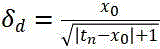
extracting brightness value of each target region of interest, and calculating contrast coefficient based on formula
The method comprises the steps of carrying out a first treatment on the surface of the Wherein:
Representing the brightness value of the substrate,/-, and>
a luminance value representing an nth target region of interest; d represents the number of contrast coefficients;
setting a contrast critical threshold Qt and correlating it with the contrast coefficient
Make a judgment if there is a contrast coefficient +.>
Marking the sapphire substrate image corresponding to the overlook defect as a corner collapse defect type if the sapphire substrate image is larger than or equal to a contrast critical threshold value Qt, and taking the sapphire substrate image corresponding to the overlook defect as a first defect type image; if there is a contrast coefficient +>
And if the contrast critical threshold value Qt is smaller than the contrast critical threshold value Qt, marking the sapphire substrate image corresponding to the overlooking defect as other defect types.
Further, the specific process of the second defect type analysis is as follows:
extracting non-edge interested areas in the top-down defect sapphire substrate images, and extracting brightness information of each pixel in the non-edge interested areas based on the non-edge interested areas;
judging whether an approximate bright spot exists based on the brightness information of each pixel, if so, taking the approximate bright spot as a reference bright spot, taking the reference bright spot as a reference to extract surrounding approximate bright spots, acquiring coordinate values of the reference bright spot and the surrounding approximate bright spot, and calculating the distance based on a formula
Wherein:
Coordinates representing reference bright spots +.>
Coordinates representing an approximate bright spot;
judging the calculated distance
If the distance is within the preset distance threshold, repeating the steps to obtain a plurality of surrounding approximate bright spots;
judging whether the total length of the reference bright spot and the plurality of surrounding approximate bright spots meets a threshold value, if so, marking the sapphire substrate image corresponding to the overlook defect as a scratch defect type, and taking the sapphire substrate image corresponding to the overlook defect as a second defect type image.
Further, the specific process of the third defect type analysis is as follows:
extracting non-edge interested areas in the top-down defect sapphire substrate images, and extracting brightness information of each pixel in the non-edge interested areas based on the non-edge interested areas;
judging whether a brightness aggregation area similar to a circle exists or not based on the brightness information of each pixel, if so, extracting a first circular area outside the brightness aggregation area in a circular searching mode, and searching a second circular area outside the first circular area according to the first circular area;
judging whether the brightness aggregation area, the first round area and the second round area of the approximate circle are in a preset brightness distinguishing rule or not;
The brightness distinguishing rule comprises a pit brightness distinguishing rule and a non-pit brightness distinguishing rule, wherein the pit brightness distinguishing rule indicates that a brightness gathering area, a first round area and a second round area which are approximate circles meet brightness distribution rules of brightness, darkness and brightness; the non-pit brightness discrimination rule indicates that the brightness aggregation area, the first circular area and the second circular area of the approximate circle meet the brightness distribution rule of brightness-darkness;
if yes, marking the sapphire substrate image corresponding to the overlook defect as a pit defect type, and taking the sapphire substrate image corresponding to the overlook defect as a third defect type image; if not, marking the images as images of other suspected defects of the sapphire substrate;
the specific process of the fourth defect type analysis is as follows:
extracting other suspected defect sapphire substrate images, and splicing a brightness aggregation area, a first circular area and a second circular area of each approximate circle meeting non-pit brightness distinguishing rules based on the images to generate i comprehensive approximate circle areas, wherein i is more than or equal to 1;
calculating the similarity, area ratio and quantity difference of every two different comprehensive approximate circle areas, and obtaining a comprehensive judgment coefficient through a formula
The method comprises the steps of carrying out a first treatment on the surface of the Wherein:
,
Representing similarity (S)>
Indicating differential numbers, ++>
Representing the area ratio;
setting a comprehensive judgment threshold value Yt, and setting the comprehensive judgment coefficient
Comparing with the comprehensive judgment threshold Yt, if the comprehensive judgment coefficient +.>
If the detection result is larger than or equal to the comprehensive judgment threshold value Yt, the sapphire substrate image corresponding to the overlook defect is indicated to be of a particle defect type, and the sapphire substrate image corresponding to the overlook defect is taken as an image of a fourth defect type; if the comprehensive judgment coefficient->
And if the detection result is smaller than the comprehensive judgment threshold value Yt, the detection result shows that the sapphire substrate image corresponding to the overlook defect is of a bubble defect type, and the sapphire substrate image corresponding to the overlook defect is taken as a fifth defect type image.
Further, the method for automatic defect detection and classification of the sapphire substrate further comprises the following steps:
s105: inputting a plurality of first defect type images, second defect type images, third defect type images, fourth defect type images and fifth defect type images into a pre-constructed generation countermeasure network respectively, and adding a defect sapphire substrate image data set based on the generation countermeasure network to acquire the first defect type images, the second defect type images, the third defect type images, the fourth defect type images and the fifth defect type images;
S106: constructing five base learners, respectively taking a first defect type image, a second defect type image, a third defect type image, a fourth defect type image and a fifth defect type image as a first type sample set, a second type sample set, a third type sample set, a fourth type sample set and a fifth type sample set, and inputting each corresponding base learner based on each type sample set to generate a first defect identification model, a second defect identification model, a third defect identification model, a fourth defect identification model and a fifth defect identification model;
s107: inputting a plurality of sapphire substrate images into a first defect recognition model, a second defect recognition model, a third defect recognition model, a fourth defect recognition model and a fifth defect recognition model to obtain first recognition data, second recognition data, third recognition data, fourth recognition data and fifth recognition data; constructing an ensemble learner, taking the first identification data, the second identification data, the third identification data, the fourth identification data and the fifth identification data as identification sample sets, dividing 70% training sets and 30% test sets, inputting 70% training sets into the ensemble learner, and training according to an ensemble learning strategy to generate a sapphire substrate detection model; testing the sapphire substrate detection model based on 30% of the test set, and outputting the sapphire substrate detection model meeting the expectation;
S108: and acquiring a plurality of sapphire substrate images to be detected, and detecting and classifying the sapphire substrate images based on the sapphire substrate detection model.
A system for automatic defect detection and classification of sapphire substrates, comprising a method for automatic defect detection and classification of sapphire substrates according to any of the above.
Compared with the prior art, the invention has the beneficial effects that:
(1) The invention discloses a method and a system for detecting and classifying automatic defects of a sapphire substrate, which are characterized in that by acquiring side view sapphire substrate images with different angles, acquiring gray scale change coefficients and brightness change coefficients based on the side view sapphire substrate images, extracting comprehensive influence coefficients, and comparing and analyzing the comprehensive influence coefficients with defect gradient criticality, the method and the system can be used for efficiently screening the sapphire substrate with defects, and compared with manual detection, the method and the system have the advantages of higher detection accuracy and higher speed; in addition, the method and the device for classifying the defects of the sapphire substrate are beneficial to providing important and efficient data support for finding problems in the substrate processing process and improving the substrate processing technology level by classifying the defects of the selected defective sapphire substrate based on the defect characteristics of the sapphire substrates of different types.
(2) The invention discloses a method and a system for automatic defect detection and classification of a sapphire substrate, which are beneficial to solving the problem of insufficient training data of the existing sapphire substrate by generating an antagonism network on the basis of acquiring a plurality of first defect type images, second defect type images, third defect type images, fourth defect type images and fifth defect type images.
Detailed Description
The following description of the embodiments of the present invention will be made clearly and completely with reference to the accompanying drawings, in which it is apparent that the embodiments described are only some embodiments of the present invention, but not all embodiments.
In the description of the present invention, it should be understood that the terms "upper," "lower," "front," "rear," "left," "right," "top," "bottom," "inner," "outer," and the like indicate or are based on the orientation or positional relationship shown in the drawings, merely to facilitate description of the present invention and to simplify the description, and do not indicate or imply that the devices or elements referred to must have a specific orientation, be configured and operated in a specific orientation, and thus should not be construed as limiting the present invention.
In the actual production process of the sapphire substrate, about 8% -15% of the sapphire substrate can generate surface defects (as shown in fig. 5), wherein in fig. 5 (a), a hole defect schematic diagram of the sapphire substrate is shown, in fig. 5 (b), a corner collapse defect schematic diagram of the sapphire substrate is shown, in fig. 5 (c), a scratch defect schematic diagram of the sapphire substrate is shown, in fig. 5 (d), a bubble defect schematic diagram of the sapphire substrate is shown, and in fig. 5 (e), a particle defect schematic diagram of the sapphire substrate is shown; the substrate surface quality has a great influence on the subsequent patterning process and the growth of the GaN epitaxial layer, so how to perform efficient automatic detection on the sapphire substrate to identify and classify the substrate defects, and further providing important data support for finding substrate processing problems and improving the substrate processing technology level becomes particularly important.
Example 1
Referring to fig. 3, an embodiment of the present invention provides a system for automatic defect detection and classification of sapphire substrates, including:
a first data acquisition module 110 for acquiring a side view sapphire substrate image based on an image acquisition device to acquire a sapphire substrate positioned on a reference substrate; the side-looking sapphire substrate image comprises a side-looking sapphire substrate image at a first angle, a side-looking sapphire substrate image at a second angle, a side-looking sapphire substrate image at a third angle and a side-looking sapphire substrate image at a fourth angle;
It should be noted that: the image acquisition equipment mainly comprises a high-resolution industrial camera and an illumination light source; the reference substrate is specifically one of a pure white reference substrate or a pure black reference substrate;
also to be described is: the side view sapphire substrate image acquisition further comprises an image preprocessing process, wherein the image preprocessing process comprises operations such as image denoising, image enhancement, image graying and the like;
specifically, the side view sapphire substrate image includes a sapphire substrate region and a reference substrate region; the side view sapphire substrate image at the first angle, the side view sapphire substrate image at the second angle, the side view sapphire substrate image at the third angle and the side view sapphire substrate image at the fourth angle are obtained based on the light collection of the irradiation light sources at the four basic angles; the four basic angles comprise four directions of northeast, northwest, southeast and southwest, and the four basic angle irradiation light sources are arranged symmetrically in coordinates;
the defect detection analysis module 120 is configured to perform a defect preliminary analysis on the side-view sapphire substrate image to obtain a plurality of defect sapphire substrate images;
it should be noted that: defects in the defect side view sapphire substrate image comprise five types of scratches, pits, bubbles, particles and angles;
Specifically, the specific process of the defect preliminary analysis is as follows:
respectively extracting gray information and brightness information of the first-angle side-looking sapphire substrate image, the second-angle side-looking sapphire substrate image, the third-angle side-looking sapphire substrate image and the fourth-angle side-looking sapphire substrate image;
information division and analysis are respectively carried out on gray information and brightness information of the side view sapphire substrate image at a first angle, the side view sapphire substrate image at a second angle, the side view sapphire substrate image at a third angle and the side view sapphire substrate image at a fourth angle so as to obtain gray change coefficients and brightness change coefficients of the side view sapphire substrate images at different angles;
the specific steps of information division and analysis of the gray information are as follows:
dividing gray level information of the side-view sapphire substrate image of each angle in an equal division manner from near to far according to the angle of the illumination direction to obtain gray level values of a plurality of gray level equal division areas, and calculating gray level change coefficients of the side-view sapphire substrate images of different angles according to the gray level values
Wherein:
Representing the gray scale coefficient,/-, and>
represents gray value, i represents gray equal division area number,/ >
Representing the total number of gray level equally divided areas;
it should be noted that: coefficient of change in gradation
The larger the side view sapphire substrate image gray scale variation range of a certain angle is, the larger the side view sapphire substrate image gray scale variation range of the certain angle is;
the specific steps of information division and analysis of the brightness information are as follows:
dividing the brightness information of the side-view sapphire substrate image of each angle from near to far according to the illumination direction angle to obtain brightness values of a plurality of brightness dividing areas, and calculating brightness change coefficients of the side-view sapphire substrate images of different angles according to the brightness values
Wherein:
Representing the brightness change coefficient, +.>
Represents the luminance value, j represents the number of luminance equally divided regions, +.>
Representing the total number of the brightness equally divided areas;
it should be noted that: coefficient of variation of luminance
The larger the side view sapphire substrate image brightness variation range of a certain angle is, the larger the side view sapphire substrate image brightness variation range of the certain angle is;
based on the gray scale change coefficients and the brightness change coefficients of a plurality of side view sapphire substrate images at different angles, carrying out comprehensive data analysis to obtain a plurality of defect sapphire substrate images;
specifically, the specific process of the comprehensive data analysis is as follows: extracting gray scale change coefficients of a first-angle side-looking sapphire substrate image, a second-angle side-looking sapphire substrate image, a third-angle side-looking sapphire substrate image and a fourth-angle side-looking sapphire substrate image
And a luminance change coefficient->
And calculating the comprehensive influence coefficient according to the total influence coefficient
Wherein:
Representing the number of side view sapphire substrate images at different angles;
setting a defect gradient critical Gt, and setting the comprehensive influence coefficient of the side-view sapphire substrate image
Comparing with defect gradient critical Gt, if the integrated influence coefficient is +.>
Greater than or equal to the defectGradient critical Gt, a first order analysis marker is generated if the integrated influence coefficient +.>
Generating a secondary analysis mark when the defect gradient critical Gt is smaller than the defect gradient critical Gt; the secondary analysis mark indicates that the corresponding side view sapphire substrate image is a defect-free sapphire substrate image; the first-level analysis mark indicates that the side view sapphire substrate image is a defective sapphire substrate image;
extracting a plurality of defective sapphire substrate images according to the first-level analysis mark;
the second data acquisition module 130 is configured to extract the plurality of defective sapphire substrate images, and acquire defective sapphire substrates located on the reference substrate through the image acquisition device according to the plurality of defective sapphire substrate images, so as to acquire a plurality of top-down defective sapphire substrate images;
it should be noted that: the irradiation light source is positioned right above the defective sapphire substrate;
The defect type dividing module 140 is configured to perform a first defect type analysis, a second defect type analysis, a third defect type analysis, and a fourth defect type analysis on a plurality of top-view defect sapphire substrate images, so as to determine the attribution of the defect types and acquire corresponding defect type images;
the defect types comprise a corner collapse defect type, a scratch defect type, a pit defect type, a particle defect type and a bubble defect type;
the corresponding defect type image comprises a first defect type image, a second defect type image, a third defect type image, a fourth defect type image and a fifth defect type image;
specifically, the specific process of the first defect type analysis is as follows:
extracting a sapphire substrate area and a reference substrate area in the top-down defect sapphire substrate image, and obtaining a substrate brightness value of the reference substrate after graying;
performing size cutting on the reference substrate region based on the sapphire substrate region, performing four-corner region division on the sapphire substrate image with the overlooking defect obtained after cutting to obtain four edge regions of interest, and performing pixel-level region of interest division on each edge region of interest to obtain a plurality of target regions of interest;
It should be noted that: the pixel-level region of interest division indicates that each target region of interest includes at least one pixel and no more than three pixels;
extracting brightness value of each target region of interest, and calculating contrast coefficient based on formula
The method comprises the steps of carrying out a first treatment on the surface of the Wherein:
The brightness value of the substrate is represented, t represents the brightness value in the target region of interest, and n represents the number of the target regions of interest; d represents the number of contrast coefficients;
setting a contrast critical threshold Qt and correlating it with the contrast coefficient
Make a judgment if there is a contrast coefficient +.>
Marking the sapphire substrate image corresponding to the overlook defect as a corner collapse defect type if the sapphire substrate image is larger than or equal to a contrast critical threshold value Qt, and taking the sapphire substrate image corresponding to the overlook defect as a first defect type image; if there is a contrast coefficient +>
And if the contrast critical threshold value Qt is smaller than the contrast critical threshold value Qt, marking the sapphire substrate image corresponding to the overlooking defect as other defect types.
Specifically, the specific process of the second defect type analysis is as follows:
extracting non-edge interested areas in the top-down defect sapphire substrate images, and extracting brightness information of each pixel in the non-edge interested areas based on the non-edge interested areas;
Judging whether an approximate bright spot exists based on the brightness information of each pixel, if so, taking the approximate bright spot as a reference bright spot, taking the reference bright spot as a reference to extract surrounding approximate bright spots, acquiring coordinate values of the reference bright spot and the surrounding approximate bright spot, and calculating the distance based on a formula
Wherein:
Coordinates representing reference bright spots +.>
Coordinates representing an approximate bright spot;
judging the calculated distance
If the distance is within the preset distance threshold, repeating the steps to obtain a plurality of surrounding approximate bright spots;
judging whether the total length of the reference bright spot and a plurality of surrounding approximate bright spots meets a threshold value, if so, marking the sapphire substrate image corresponding to the overlook defect as a scratch defect type, and taking the sapphire substrate image corresponding to the overlook defect as a second defect type image;
specifically, the specific process of the third defect type analysis is as follows:
extracting non-edge interested areas in the top-down defect sapphire substrate images, and extracting brightness information of each pixel in the non-edge interested areas based on the non-edge interested areas;
judging whether a brightness aggregation area similar to a circle exists or not based on the brightness information of each pixel, if so, extracting a first circular area outside the brightness aggregation area in a circular searching mode, and searching a second circular area outside the first circular area according to the first circular area;
Judging whether the brightness aggregation area, the first round area and the second round area of the approximate circle are in a preset brightness distinguishing rule or not;
specifically, the brightness distinguishing rule comprises a pit brightness distinguishing rule and a non-pit brightness distinguishing rule, wherein the pit brightness distinguishing rule represents that a brightness gathering area, a first round area and a second round area which are approximate circles meet a brightness distribution rule of brightness, darkness and brightness; the non-pit brightness discrimination rule indicates that the brightness aggregation area, the first circular area and the second circular area of the approximate circle meet the brightness distribution rule of brightness-darkness;
it should be noted that: according to the principle of illumination development, pit defects in an image are generally in brightness distribution of bright center and dark inner wall, and bright pit corners, namely bright-dark-bright; the bubbles in the image are generally in bright center and dark brightness distribution around, namely bright-dark, and the same is true; the particles are similar to the bubble brightness distribution; however, the size of the bubbles is generally larger than the particles, and the number of particles is relatively large;
if yes, marking the sapphire substrate image corresponding to the overlook defect as a pit defect type, and taking the sapphire substrate image corresponding to the overlook defect as a third defect type image; if not, marking the images as images of other suspected defects of the sapphire substrate;
Specifically, the specific process of the fourth defect type analysis is as follows:
extracting other suspected defect sapphire substrate images, and splicing a brightness aggregation area, a first circular area and a second circular area of each approximate circle meeting non-pit brightness distinguishing rules based on the images to generate i comprehensive approximate circle areas, wherein i is more than or equal to 1;
obtaining the range area of particles in the preset template defect image, calculating the similarity, area ratio and perimeter difference between the particle and each comprehensive approximate circle area, and obtaining the comprehensive judgment coefficient through a formula
The method comprises the steps of carrying out a first treatment on the surface of the Wherein:
,
representing similarity (S)>
Indicating the difference in circumference, +.>
Representing the area ratio;
setting a comprehensive judgment threshold value Yt, and setting the comprehensive judgment coefficient
Comparing with the comprehensive judgment threshold Yt, if the comprehensive judgment coefficient +.>
If the detection result is larger than or equal to the comprehensive judgment threshold value Yt, the sapphire substrate image corresponding to the overlook defect is indicated to be of a particle defect type, and the sapphire substrate image corresponding to the overlook defect is taken as an image of a fourth defect type; if the comprehensive judgment coefficient->
If the detection result is smaller than the comprehensive judgment threshold value Yt, the sapphire substrate image corresponding to the overlook defect is indicated to be of a bubble defect type, and the sapphire substrate image corresponding to the overlook defect is taken as a fifth defect type image;
According to the invention, compared with manual detection, the sapphire substrate with defects can be efficiently screened, and the detection accuracy is higher and the detection speed is faster; in addition, the method and the device for classifying the defects of the sapphire substrate are beneficial to providing important and efficient data support for finding problems in the substrate processing process and improving the substrate processing technology level by classifying the defects of the selected defective sapphire substrate based on the defect characteristics of the sapphire substrates of different types.
Example 2
Referring to fig. 4, in order to improve the automation degree and make the present invention suitable for a large-scale production inspection scene, and solve the problem of a small existing sapphire substrate inspection data set, the embodiment of the present invention provides a system for automatic defect inspection classification of a sapphire substrate, which further includes:
the data set expansion module 150 is configured to input a plurality of first defect type images, second defect type images, third defect type images, fourth defect type images, and fifth defect type images into the pre-construction generation countermeasure network; and based on the incremental defect sapphire substrate image dataset, obtaining a plurality of first, second, third, fourth, and fifth defect type images;
A single model generating module 160, configured to construct five base learners, and respectively use the first defect type image, the second defect type image, the third defect type image, the fourth defect type image, and the fifth defect type image as a first type sample set, a second type sample set, a third type sample set, a fourth type sample set, and a fifth type sample set; and inputting each corresponding basis learner based on each type sample set to generate a first defect identification model, a second defect identification model, a third defect identification model, a fourth defect identification model, and a fifth defect identification model;
the ensemble learning module 170 is configured to input a plurality of sapphire substrate images into a first defect recognition model, a second defect recognition model, a third defect recognition model, a fourth defect recognition model, and a fifth defect recognition model to obtain first recognition data, second recognition data, third recognition data, fourth recognition data, and fifth recognition data; constructing an ensemble learner, taking the first identification data, the second identification data, the third identification data, the fourth identification data and the fifth identification data as identification sample sets, dividing 70% training sets and 30% test sets, inputting 70% training sets into the ensemble learner, and training according to an ensemble learning strategy to generate a sapphire substrate detection model; testing the sapphire substrate detection model based on 30% of the test set, and outputting the sapphire substrate detection model meeting the expectation;
It should be noted that: the integrated learner is specifically a convolutional neural network, and the integrated learning strategy is specifically a weighted average strategy;
in this embodiment, the system further includes a third data acquisition module 180, where the third data acquisition module is configured to acquire, by using an image acquisition device, a plurality of images of the sapphire substrate to be detected that are located on the reference substrate;
in this example, the inspection defect analysis module 120 is further configured to integrate the sapphire substrate inspection model that meets the expectation, and inspect and classify a plurality of the sapphire substrate images to be inspected based thereon;
on the basis of acquiring a plurality of first defect type images, second defect type images, third defect type images, fourth defect type images and fifth defect type images, the invention is favorable for solving the problem of insufficient training data of the existing sapphire substrate by generating an countermeasure network, in addition, the invention carries out single model training on the expanded data set and acquires the output result of the single model, and then carries out fusion training on the output results of a plurality of single models through integrated learning to acquire a sapphire substrate detection model and detect and classify the images of the sapphire substrate to be detected based on the sapphire substrate detection model.
Example 3
Referring to fig. 1, an embodiment of the present invention provides a method for automatic defect detection and classification of a sapphire substrate, including:
s101: acquiring a sapphire substrate positioned on a reference substrate based on an image acquisition device to acquire a side-view sapphire substrate image; the side-looking sapphire substrate image comprises a side-looking sapphire substrate image at a first angle, a side-looking sapphire substrate image at a second angle, a side-looking sapphire substrate image at a third angle and a side-looking sapphire substrate image at a fourth angle;
it should be noted that: the image acquisition equipment mainly comprises a high-resolution industrial camera and an illumination light source; the reference substrate is specifically one of a pure white reference substrate or a pure black reference substrate;
also to be described is: the side view sapphire substrate image acquisition further comprises an image preprocessing process, wherein the image preprocessing process comprises operations such as image denoising, image enhancement, image graying and the like;
specifically, the side view sapphire substrate image includes a sapphire substrate region and a reference substrate region; the side view sapphire substrate image at the first angle, the side view sapphire substrate image at the second angle, the side view sapphire substrate image at the third angle and the side view sapphire substrate image at the fourth angle are obtained based on the light collection of the irradiation light sources at the four basic angles; the four basic angles comprise four directions of northeast, northwest, southeast and southwest, and the four basic angle irradiation light sources are arranged symmetrically in coordinates;
S102: performing defect preliminary analysis on the side view sapphire substrate image to obtain a plurality of defect sapphire substrate images;
it should be noted that: defects in the defect side view sapphire substrate image comprise five types of scratches, pits, bubbles, particles and angles;
specifically, the specific process of the defect preliminary analysis is as follows:
respectively extracting gray information and brightness information of the first-angle side-looking sapphire substrate image, the second-angle side-looking sapphire substrate image, the third-angle side-looking sapphire substrate image and the fourth-angle side-looking sapphire substrate image;
information division and analysis are respectively carried out on gray information and brightness information of the side view sapphire substrate image at a first angle, the side view sapphire substrate image at a second angle, the side view sapphire substrate image at a third angle and the side view sapphire substrate image at a fourth angle so as to obtain gray change coefficients and brightness change coefficients of the side view sapphire substrate images at different angles;
the specific steps of information division and analysis of the gray information are as follows:
imaging side view sapphire substrates at each angleDividing gray information from near to far according to illumination direction angles to obtain gray values of a plurality of gray dividing areas, and calculating gray change coefficients of side-view sapphire substrate images of different angles according to the gray values
Wherein:
Representing the gray scale coefficient,/-, and>
represents gray value, i represents gray equal division area number,
Representing the total number of gray level equally divided areas;
it should be noted that: coefficient of change in gradation
The larger the side view sapphire substrate image gray scale variation range of a certain angle is, the larger the side view sapphire substrate image gray scale variation range of the certain angle is;
the specific steps of information division and analysis of the brightness information are as follows:
dividing the brightness information of the side-view sapphire substrate image of each angle from near to far according to the illumination direction angle to obtain brightness values of a plurality of brightness dividing areas, and calculating brightness change coefficients of the side-view sapphire substrate images of different angles according to the brightness values
Wherein:
Representing the brightness change coefficient, +.>
Represents the luminance value, j represents the number of luminance equally divided regions, +.>
Indicating partitions such as brightnessTotal number of domains;
it should be noted that: coefficient of variation of luminance
The larger the side view sapphire substrate image brightness variation range of a certain angle is, the larger the side view sapphire substrate image brightness variation range of the certain angle is;
based on the gray scale change coefficients and the brightness change coefficients of a plurality of side view sapphire substrate images at different angles, carrying out comprehensive data analysis to obtain a plurality of defect sapphire substrate images;
specifically, the specific process of the comprehensive data analysis is as follows: extracting gray scale change coefficients of a first-angle side-looking sapphire substrate image, a second-angle side-looking sapphire substrate image, a third-angle side-looking sapphire substrate image and a fourth-angle side-looking sapphire substrate image
And a luminance change coefficient->
And calculating the comprehensive influence coefficient according to the total influence coefficient
Wherein:
Representing the number of side view sapphire substrate images at different angles;
setting a defect gradient critical Gt, and setting the comprehensive influence coefficient of the side-view sapphire substrate image
Comparing with defect gradient critical Gt, if the integrated influence coefficient is +.>
Generating a first-order analysis mark if the defect gradient critical Gt is larger than or equal to the defect gradient critical Gt, and if the comprehensive influence coefficient is +.>
Less than the defectGradient critical Gt, then generating a secondary analysis mark; the secondary analysis mark indicates that the corresponding side view sapphire substrate image is a defect-free sapphire substrate image; the first-level analysis mark indicates that the side view sapphire substrate image is a defective sapphire substrate image;
extracting a plurality of defective sapphire substrate images according to the first-level analysis mark;
s103: extracting the plurality of defect sapphire substrate images, and collecting a plurality of overlooking defect sapphire substrate images on a reference substrate through an image collecting device according to the defect sapphire substrate images;
it should be noted that: the irradiation light source is positioned right above the defective sapphire substrate;
s104: performing first defect type analysis, second defect type analysis, third defect type analysis and fourth defect type analysis on a plurality of top-down defect sapphire substrate images to determine defect type attribution and acquire corresponding defect type images;
The defect types comprise a corner collapse defect type, a scratch defect type, a pit defect type, a particle defect type and a bubble defect type;
the corresponding defect type image comprises a first defect type image, a second defect type image, a third defect type image, a fourth defect type image and a fifth defect type image;
specifically, the specific process of the first defect type analysis is as follows:
extracting a sapphire substrate area and a reference substrate area in the top-down defect sapphire substrate image, and obtaining a substrate brightness value of the reference substrate after graying;
performing size cutting on the reference substrate region based on the sapphire substrate region, performing four-corner region division on the sapphire substrate image with the overlooking defect obtained after cutting to obtain four edge regions of interest, and performing pixel-level region of interest division on each edge region of interest to obtain a plurality of target regions of interest;
it should be noted that: the pixel-level region of interest division indicates that each target region of interest includes at least one pixel and no more than three pixels;
extracting brightness value of each target region of interest, and calculating contrast coefficient based on formula
The method comprises the steps of carrying out a first treatment on the surface of the Wherein:
Representing the brightness value of the substrate,/-, and>
a luminance value representing an nth target region of interest; d represents the number of contrast coefficients;
setting a contrast critical threshold Qt and correlating it with the contrast coefficient
Make a judgment if there is a contrast coefficient +.>
Marking the sapphire substrate image corresponding to the overlook defect as a corner collapse defect type if the sapphire substrate image is larger than or equal to a contrast critical threshold value Qt, and taking the sapphire substrate image corresponding to the overlook defect as a first defect type image; if there is a contrast coefficient +>
And if the contrast critical threshold value Qt is smaller than the contrast critical threshold value Qt, marking the sapphire substrate image corresponding to the overlooking defect as other defect types.
Specifically, the specific process of the second defect type analysis is as follows:
extracting non-edge interested areas in the top-down defect sapphire substrate images, and extracting brightness information of each pixel in the non-edge interested areas based on the non-edge interested areas;
judging whether an approximate bright point exists or not based on the brightness information of each pixel, if so, taking the approximate bright point as a reference bright point, extracting surrounding approximate bright points by taking the reference bright point as a reference, and acquiring a referenceCoordinate values of the bright spots and the surrounding approximate bright spots, and calculating the distance based on a formula
Wherein:
Coordinates representing reference bright spots +.>
Coordinates representing an approximate bright spot;
judging the calculated distance
If the distance is within the preset distance threshold, repeating the steps to obtain a plurality of surrounding approximate bright spots;
judging whether the total length of the reference bright spot and a plurality of surrounding approximate bright spots meets a threshold value, if so, marking the sapphire substrate image corresponding to the overlook defect as a scratch defect type, and taking the sapphire substrate image corresponding to the overlook defect as a second defect type image;
specifically, the specific process of the third defect type analysis is as follows:
extracting non-edge interested areas in the top-down defect sapphire substrate images, and extracting brightness information of each pixel in the non-edge interested areas based on the non-edge interested areas;
judging whether a brightness aggregation area similar to a circle exists or not based on the brightness information of each pixel, if so, extracting a first circular area outside the brightness aggregation area in a circular searching mode, and searching a second circular area outside the first circular area according to the first circular area;
judging whether the brightness aggregation area, the first round area and the second round area of the approximate circle are in a preset brightness distinguishing rule or not;
Specifically, the brightness distinguishing rule comprises a pit brightness distinguishing rule and a non-pit brightness distinguishing rule, wherein the pit brightness distinguishing rule represents that a brightness gathering area, a first round area and a second round area which are approximate circles meet a brightness distribution rule of brightness, darkness and brightness; the non-pit brightness discrimination rule indicates that the brightness aggregation area, the first circular area and the second circular area of the approximate circle meet the brightness distribution rule of brightness-darkness;
it should be noted that: according to the principle of illumination development, pit defects in an image are generally in brightness distribution of bright center and dark inner wall, and bright pit corners, namely bright-dark-bright; the bubbles in the image are generally in bright center and dark brightness distribution around, namely bright-dark, and the same is true; the particles are similar to the bubble brightness distribution; however, the size of the bubbles is generally larger than the particles, and the number of particles is relatively large;
if yes, marking the sapphire substrate image corresponding to the overlook defect as a pit defect type, and taking the sapphire substrate image corresponding to the overlook defect as a third defect type image; if not, marking the images as images of other suspected defects of the sapphire substrate;
specifically, the specific process of the fourth defect type analysis is as follows:
Extracting other suspected defect sapphire substrate images, and splicing a brightness aggregation area, a first circular area and a second circular area of each approximate circle meeting non-pit brightness distinguishing rules based on the images to generate i comprehensive approximate circle areas, wherein i is more than or equal to 1;
calculating the similarity, area ratio and quantity difference of every two different comprehensive approximate circle areas, and obtaining a comprehensive judgment coefficient through a formula
The method comprises the steps of carrying out a first treatment on the surface of the Wherein:
,
Representing similarity (S)>
Indicating differential numbers, ++>
Representing the area ratio;
setting a comprehensive judgment threshold value Yt, and setting the comprehensive judgment coefficient
Comparing with the comprehensive judgment threshold Yt, if the comprehensive judgment coefficient +.>
If the detection result is larger than or equal to the comprehensive judgment threshold value Yt, the sapphire substrate image corresponding to the overlook defect is indicated to be of a particle defect type, and the sapphire substrate image corresponding to the overlook defect is taken as an image of a fourth defect type; and if the comprehensive judgment coefficient is smaller than the comprehensive judgment threshold value Yt, the sapphire substrate image corresponding to the overlook defect is indicated to be of a bubble defect type, and the sapphire substrate image corresponding to the overlook defect is taken as a fifth defect type image.
Example 4
Referring to fig. 2, based on the third embodiment, in order to improve the automation degree and make the present invention suitable for a large-scale production detection scenario, and solve the problem of a small number of existing sapphire substrate detection data sets, and the problem of low accuracy and low speed of the existing sapphire substrate detection method based on machine learning, the embodiment of the present invention provides a method for detecting and classifying automatic defects of a sapphire substrate, which further includes:
S105: inputting a plurality of first defect type images, second defect type images, third defect type images, fourth defect type images and fifth defect type images into a pre-constructed generation countermeasure network respectively, and adding a defect sapphire substrate image data set based on the generation countermeasure network to acquire the first defect type images, the second defect type images, the third defect type images, the fourth defect type images and the fifth defect type images;
s106: constructing five base learners, respectively taking a first defect type image, a second defect type image, a third defect type image, a fourth defect type image and a fifth defect type image as a first type sample set, a second type sample set, a third type sample set, a fourth type sample set and a fifth type sample set, and inputting each corresponding base learner based on each type sample set to generate a first defect identification model, a second defect identification model, a third defect identification model, a fourth defect identification model and a fifth defect identification model;
it should be noted that: the five base learners can be homogeneous base learners and heterogeneous base learners, and are specifically one or more of SVM, K neighbor, support vector machine, naive Bayes and neural network, and any machine learning model can be used as an application object of the invention, so that the invention does not limit the application object too much;
S107: inputting a plurality of sapphire substrate images into a first defect recognition model, a second defect recognition model, a third defect recognition model, a fourth defect recognition model and a fifth defect recognition model to obtain first recognition data, second recognition data, third recognition data, fourth recognition data and fifth recognition data; constructing an ensemble learner, taking the first identification data, the second identification data, the third identification data, the fourth identification data and the fifth identification data as identification sample sets, dividing 70% training sets and 30% test sets, inputting 70% training sets into the ensemble learner, and training according to an ensemble learning strategy to generate a sapphire substrate detection model; testing the sapphire substrate detection model based on 30% of the test set, and outputting the sapphire substrate detection model meeting the expectation;
s108: and acquiring a plurality of sapphire substrate images to be detected, and detecting and classifying the sapphire substrate images based on the sapphire substrate detection model.
The foregoing is only a preferred embodiment of the present invention, but the scope of the present invention is not limited thereto, and any person skilled in the art, who is within the scope of the present invention, should make equivalent substitutions or modifications according to the technical scheme of the present invention and the inventive concept thereof, and should be covered by the scope of the present invention.