CN115547233A - A pixel driving circuit, its driving method, and a display panel - Google Patents
A pixel driving circuit, its driving method, and a display panel Download PDFInfo
- Publication number
- CN115547233A CN115547233A CN202110739724.8A CN202110739724A CN115547233A CN 115547233 A CN115547233 A CN 115547233A CN 202110739724 A CN202110739724 A CN 202110739724A CN 115547233 A CN115547233 A CN 115547233A
- Authority
- CN
- China
- Prior art keywords
- module
- terminal
- transistor
- control
- electrically connected
- Prior art date
- Legal status (The legal status is an assumption and is not a legal conclusion. Google has not performed a legal analysis and makes no representation as to the accuracy of the status listed.)
- Granted
Links
Images


Classifications
-
- G—PHYSICS
- G09—EDUCATION; CRYPTOGRAPHY; DISPLAY; ADVERTISING; SEALS
- G09G—ARRANGEMENTS OR CIRCUITS FOR CONTROL OF INDICATING DEVICES USING STATIC MEANS TO PRESENT VARIABLE INFORMATION
- G09G3/00—Control arrangements or circuits, of interest only in connection with visual indicators other than cathode-ray tubes
- G09G3/20—Control arrangements or circuits, of interest only in connection with visual indicators other than cathode-ray tubes for presentation of an assembly of a number of characters, e.g. a page, by composing the assembly by combination of individual elements arranged in a matrix no fixed position being assigned to or needed to be assigned to the individual characters or partial characters
- G09G3/22—Control arrangements or circuits, of interest only in connection with visual indicators other than cathode-ray tubes for presentation of an assembly of a number of characters, e.g. a page, by composing the assembly by combination of individual elements arranged in a matrix no fixed position being assigned to or needed to be assigned to the individual characters or partial characters using controlled light sources
- G09G3/30—Control arrangements or circuits, of interest only in connection with visual indicators other than cathode-ray tubes for presentation of an assembly of a number of characters, e.g. a page, by composing the assembly by combination of individual elements arranged in a matrix no fixed position being assigned to or needed to be assigned to the individual characters or partial characters using controlled light sources using electroluminescent panels
- G09G3/32—Control arrangements or circuits, of interest only in connection with visual indicators other than cathode-ray tubes for presentation of an assembly of a number of characters, e.g. a page, by composing the assembly by combination of individual elements arranged in a matrix no fixed position being assigned to or needed to be assigned to the individual characters or partial characters using controlled light sources using electroluminescent panels semiconductive, e.g. using light-emitting diodes [LED]
- G09G3/3208—Control arrangements or circuits, of interest only in connection with visual indicators other than cathode-ray tubes for presentation of an assembly of a number of characters, e.g. a page, by composing the assembly by combination of individual elements arranged in a matrix no fixed position being assigned to or needed to be assigned to the individual characters or partial characters using controlled light sources using electroluminescent panels semiconductive, e.g. using light-emitting diodes [LED] organic, e.g. using organic light-emitting diodes [OLED]
- G09G3/3225—Control arrangements or circuits, of interest only in connection with visual indicators other than cathode-ray tubes for presentation of an assembly of a number of characters, e.g. a page, by composing the assembly by combination of individual elements arranged in a matrix no fixed position being assigned to or needed to be assigned to the individual characters or partial characters using controlled light sources using electroluminescent panels semiconductive, e.g. using light-emitting diodes [LED] organic, e.g. using organic light-emitting diodes [OLED] using an active matrix
Landscapes
- Engineering & Computer Science (AREA)
- Physics & Mathematics (AREA)
- Computer Hardware Design (AREA)
- General Physics & Mathematics (AREA)
- Theoretical Computer Science (AREA)
- Control Of Indicators Other Than Cathode Ray Tubes (AREA)
Abstract
本发明公开了一种像素驱动电路及其驱动方法、显示面板。像素驱动电路包括:模拟数据写入模块、驱动模块、存储模块、发光模块、数字数据写入模块、第一参考电压写入模块和数字信号发光控制模块;模拟数据写入模块用于将模拟数据写入驱动模块;数字数据写入模块用于将数字数据写入数字信号发光控制模块的控制端,数字信号发光控制模块根据数字数据导通;第一参考电压写入模块用于将第一参考电压写入数字信号发光控制模块的控制端,数字信号发光控制模块根据第一参考电压关断。本发明达到了更好的灰阶展开的效果,并且可以准确控制发光模块的关闭,使得发光模块更好的显示待显示亮度,提高了显示面板的显示效果。
The invention discloses a pixel driving circuit, a driving method thereof, and a display panel. The pixel driving circuit includes: an analog data writing module, a driving module, a storage module, a light emitting module, a digital data writing module, a first reference voltage writing module and a digital signal lighting control module; the analog data writing module is used to write the analog data write drive module; the digital data writing module is used to write digital data into the control terminal of the digital signal lighting control module, and the digital signal lighting control module is turned on according to the digital data; the first reference voltage writing module is used to write the first reference voltage The voltage is written into the control terminal of the digital signal lighting control module, and the digital signal lighting control module is turned off according to the first reference voltage. The invention achieves a better effect of gray scale expansion, and can accurately control the closing of the light-emitting module, so that the light-emitting module can better display the brightness to be displayed, and the display effect of the display panel is improved.
Description
技术领域technical field
本发明实施例涉及显示技术领域,尤其涉及一种像素驱动电路及其驱动方法、显示面板。The embodiments of the present invention relate to the field of display technology, and in particular, to a pixel driving circuit, a driving method thereof, and a display panel.
背景技术Background technique
随着显示技术的发展,显示面板的应用越来越广泛,相应的对显示面板的要求也越来越高。With the development of the display technology, the application of the display panel is more and more extensive, and correspondingly, the requirement for the display panel is also higher and higher.
现有的显示面板难以将所有的灰阶展开,灰阶亮度容易产生突变,影响显示面板的显示效果,且在像素驱动电路利用数字和模拟混合驱动时,难以准确控制发光模块的关断。It is difficult for existing display panels to expand all the gray scales, and the brightness of gray scales is prone to sudden changes, which affects the display effect of the display panel, and it is difficult to accurately control the shutdown of the light emitting module when the pixel driving circuit uses digital and analog hybrid driving.
发明内容Contents of the invention
本发明提供一种像素驱动电路及其驱动方法、显示面板,以实现更好的灰阶展开,提高显示面板的显示效果,且在像素驱动电路利用数字和模拟混合驱动时,实现准确控制发光模块的关断。The present invention provides a pixel driving circuit, its driving method, and a display panel, so as to realize better grayscale expansion, improve the display effect of the display panel, and realize accurate control of the light-emitting module when the pixel driving circuit uses digital and analog hybrid driving off.
第一方面,本发明实施例提供了一种像素驱动电路,该像素驱动电路包括:模拟数据写入模块、驱动模块、存储模块、发光模块、数字数据写入模块、第一参考电压写入模块和数字信号发光控制模块;In the first aspect, an embodiment of the present invention provides a pixel driving circuit, which includes: an analog data writing module, a driving module, a storage module, a light emitting module, a digital data writing module, and a first reference voltage writing module and digital signal lighting control module;
所述模拟数据写入模块用于将模拟数据写入所述驱动模块,所述驱动模块用于产生驱动电流,所述发光模块用于响应所述驱动电流,所述存储模块用于维持所述驱动模块的控制端的电位;The analog data writing module is used to write analog data into the driving module, the driving module is used to generate a driving current, the light emitting module is used to respond to the driving current, and the storage module is used to maintain the The potential of the control terminal of the drive module;
所述数字数据写入模块用于将数字数据写入所述数字信号发光控制模块的控制端,所述数字信号发光控制模块根据所述数字数据导通;The digital data writing module is used to write digital data into the control terminal of the digital signal lighting control module, and the digital signal lighting control module is turned on according to the digital data;
所述第一参考电压写入模块用于将第一参考电压写入所述数字信号发光控制模块的控制端,所述数字信号发光控制模块根据所述第一参考电压关断。The first reference voltage writing module is used to write a first reference voltage into the control terminal of the digital signal lighting control module, and the digital signal lighting control module is turned off according to the first reference voltage.
可选地,所述数字数据写入模块包括第一晶体管,所述第一参考电压写入模块包括第二晶体管;Optionally, the digital data writing module includes a first transistor, and the first reference voltage writing module includes a second transistor;
所述第一晶体管的控制端接入第一扫描信号,所述第一晶体管的第一端用于写入所述数字数据,所述第一晶体管的第二端与所述数字信号发光控制模块的控制端电连接;The control end of the first transistor is connected to the first scan signal, the first end of the first transistor is used to write the digital data, the second end of the first transistor is connected to the digital signal light emitting control module The control terminal is electrically connected;
所述第二晶体管的控制端接入第一控制信号,所述第二晶体管的第一端用于写入所述第一参考电压,所述第二晶体管的第二端与所述数字信号发光控制模块的控制端电连接。The control terminal of the second transistor is connected to the first control signal, the first terminal of the second transistor is used to write the first reference voltage, and the second terminal of the second transistor is connected to the digital signal to emit light The control terminal of the control module is electrically connected.
可选地,所述数字数据写入模块还包括第三晶体管,所述第一参考电压写入模块还包括第四晶体管;Optionally, the digital data writing module further includes a third transistor, and the first reference voltage writing module further includes a fourth transistor;
所述第三晶体管的控制端用于接入第二扫描信号,所述第三晶体管的第一端与所述第一晶体管的第一端电连接,所述第三晶体管的第二端与所述第一晶体管的第二端电连接;所述第一扫描信号与所述第二扫描信号相位相反,所述第一晶体管为N型晶体管,所述第三晶体管为P型晶体管;The control end of the third transistor is used to access the second scan signal, the first end of the third transistor is electrically connected to the first end of the first transistor, and the second end of the third transistor is electrically connected to the first end of the third transistor. The second terminal of the first transistor is electrically connected; the phase of the first scanning signal is opposite to that of the second scanning signal, the first transistor is an N-type transistor, and the third transistor is a P-type transistor;
所述第四晶体管的控制端接入第二控制信号,所述第四晶体管的第一端与所述第二晶体管的第一端电连接,所述第四晶体管的第二端与所述第二晶体管的第二端电连接;所述第一控制信号与所述第二控制信号相位相反,所述第二晶体管为P型晶体管,所述第四晶体管为N型晶体管。The control terminal of the fourth transistor is connected to the second control signal, the first terminal of the fourth transistor is electrically connected to the first terminal of the second transistor, and the second terminal of the fourth transistor is connected to the first terminal of the first transistor. The second terminals of the two transistors are electrically connected; the phase of the first control signal is opposite to that of the second control signal, the second transistor is a P-type transistor, and the fourth transistor is an N-type transistor.
可选地,像素驱动电路还包括锁存模块;Optionally, the pixel driving circuit also includes a latch module;
所述锁存模块用于维持所述数字信号发光控制模块的控制端的电位。The latch module is used to maintain the potential of the control terminal of the digital signal lighting control module.
可选地,所述锁存模块包括第一反相器和第二反相器,所述第一反相器的输入端与所述数字信号发光控制模块的控制端电连接,所述第一反相器的输出端与所述第二反相器的输入端电连接,所述第二反相器的输出端与所述第一晶体管的第二端电连接;Optionally, the latch module includes a first inverter and a second inverter, the input end of the first inverter is electrically connected to the control end of the digital signal lighting control module, and the first inverter The output end of the inverter is electrically connected to the input end of the second inverter, and the output end of the second inverter is electrically connected to the second end of the first transistor;
或者,所述锁存模块包括第一电容,所述第一电容的第一端接入第一电源信号,所述第一电容的第二端与所述数字信号发光控制模块的控制端电连接。Alternatively, the latch module includes a first capacitor, the first end of the first capacitor is connected to the first power supply signal, and the second end of the first capacitor is electrically connected to the control end of the digital signal lighting control module .
可选地,所述模拟数据写入模块的控制端接入第三扫描信号,所述模拟数据写入模块的第一端用于写入模拟数据,所述模拟数据写入模块的第二端与所述驱动模块的控制端电连接;Optionally, the control end of the analog data writing module is connected to the third scan signal, the first end of the analog data writing module is used to write analog data, and the second end of the analog data writing module electrically connected to the control terminal of the drive module;
所述驱动模块的第一端用于连接第一电源信号,所述驱动模块的第二端与所述数字信号发光控制模块的第一端电连接,所述数字信号发光控制模块的第二端与所述发光模块的第一端电连接,所述发光模块的第二端连接第二电源信号;The first end of the driving module is used to connect the first power signal, the second end of the driving module is electrically connected to the first end of the digital signal lighting control module, and the second end of the digital signal lighting control module It is electrically connected to the first end of the light emitting module, and the second end of the light emitting module is connected to the second power signal;
所述存储模块的第一端连接所述第一电源信号,所述存储模块的第二端与所述驱动模块的控制端电连接;The first terminal of the storage module is connected to the first power signal, and the second terminal of the storage module is electrically connected to the control terminal of the drive module;
所述数字数据写入模块的第一端接入数字数据,所述数字数据写入模块的第二端与所述数字信号发光控制模块的控制端电连接;The first end of the digital data writing module is connected to digital data, and the second end of the digital data writing module is electrically connected to the control end of the digital signal lighting control module;
所述第一参考电压写入模块的第一端接入第一参考电压,所述第一参考电压写入模块的第二端与所述数字信号发光控制模块的控制端电连接。The first terminal of the first reference voltage writing module is connected to the first reference voltage, and the second terminal of the first reference voltage writing module is electrically connected to the control terminal of the digital signal lighting control module.
可选地,像素驱动电路还包括第一初始化模块、第二初始化模块、阈值补偿模块、第一模拟信号发光控制模块和第二模拟信号发光控制模块;Optionally, the pixel driving circuit further includes a first initialization module, a second initialization module, a threshold compensation module, a first analog signal light emission control module, and a second analog signal light emission control module;
所述第一初始化模块的控制端接入第四扫描信号,所述第一初始化模块的第一端接入第二参考电压,所述第一初始化模块的第二端与驱动模块的控制端电连接,所述存储模块的第一端与所述驱动模块的控制端电连接,所述存储模块的第二端连接第一电源信号;所述第一初始化模块用于初始化所述驱动模块;The control terminal of the first initialization module is connected to the fourth scanning signal, the first terminal of the first initialization module is connected to the second reference voltage, and the second terminal of the first initialization module is electrically connected to the control terminal of the driving module. connected, the first end of the storage module is electrically connected to the control end of the drive module, and the second end of the storage module is connected to a first power signal; the first initialization module is used to initialize the drive module;
所述第二初始化模块的控制端接入所述第四扫描信号,所述第二初始化模块的第一端接入所述第二参考电压,所述第二初始化模块的第二端与所述发光模块的第一端电连接;所述第二初始化模块用于初始化所述发光模块;The control terminal of the second initialization module is connected to the fourth scan signal, the first terminal of the second initialization module is connected to the second reference voltage, the second terminal of the second initialization module is connected to the The first end of the light emitting module is electrically connected; the second initialization module is used to initialize the light emitting module;
所述模拟数据写入模块的控制端接入第三扫描信号,所述模拟数据写入模块的第一端用于写入模拟数据,所述模拟数据写入模块的第二端与所述驱动模块的第一端电连接;The control end of the analog data writing module is connected to the third scan signal, the first end of the analog data writing module is used to write analog data, the second end of the analog data writing module is connected to the drive the first end of the module is electrically connected;
所述驱动模块的第一端与所述第一模拟信号发光控制模块的第一端电连接,所述驱动模块的第二端与所述第二模拟信号发光控制模块的第一端电连接;The first end of the driving module is electrically connected to the first end of the first analog signal lighting control module, and the second end of the driving module is electrically connected to the first end of the second analog signal lighting control module;
所述第一模拟信号发光控制模块的控制端接入使能信号,所述第一模拟信号发光控制模块的第二端与所述第一电源信号电连接;The control terminal of the first analog signal lighting control module is connected to the enabling signal, and the second terminal of the first analog signal lighting control module is electrically connected to the first power supply signal;
所述阈值补偿模块的控制端接入所述第三扫描信号,所述阈值补偿模块的第一端与所述驱动模块的控制端电连接,所述阈值补偿模块的第二端与所述第二模拟信号发光控制模块的第一端电连接;所述阈值补偿模块用于抓取所述驱动模块的阈值电压至所述驱动模块的控制端;The control terminal of the threshold compensation module is connected to the third scan signal, the first terminal of the threshold compensation module is electrically connected to the control terminal of the driving module, and the second terminal of the threshold compensation module is connected to the second terminal of the threshold compensation module. The first terminals of the two analog signal lighting control modules are electrically connected; the threshold compensation module is used to capture the threshold voltage of the driving module to the control terminal of the driving module;
所述第二模拟信号发光控制模块的控制端接入所述使能信号,所述第二模拟信号发光控制模块的第二端与所述数字信号发光控制模块电连接。The control terminal of the second analog signal lighting control module is connected to the enabling signal, and the second terminal of the second analog signal lighting control module is electrically connected to the digital signal lighting control module.
第二方面,本发明实施例还提供了一种像素驱动电路的驱动方法,用于驱动第一方面任意所述的像素驱动电路,所述像素驱动电路的驱动方法包括:In the second aspect, an embodiment of the present invention further provides a driving method of a pixel driving circuit, which is used to drive any of the pixel driving circuits described in the first aspect, and the driving method of the pixel driving circuit includes:
获取待显示亮度;Obtain the brightness to be displayed;
判断所述待显示亮度是否满足预设条件;judging whether the brightness to be displayed satisfies a preset condition;
若所述待显示亮度满足预设条件,则根据所述待显示亮度确定所述模拟数据;在数据写入阶段将所述模拟数据写入所述驱动模块,并在发光阶段将所述数字数据持续写入所述数字信号发光控制模块;If the brightness to be displayed satisfies the preset condition, then determine the analog data according to the brightness to be displayed; write the analog data into the drive module in the data writing phase, and write the digital data in the light emitting phase Continuously write the digital signal to the lighting control module;
若所述待显示亮度不满足预设条件,则根据所述待显示亮度确定所述数字数据写入模块的第一导通时间以及所述第一参考电压写入模块的第二导通时间;在数据写入阶段将模拟数据写入所述驱动模块,并在第一导通时间将所述数字数据写入所述数字发光控制模块的控制端,在第二导通时间将所述第一参考电压写入所述数字发光控制模块的控制端,其中,所述模拟数据为固定值。If the brightness to be displayed does not meet the preset condition, then determine the first conduction time of the digital data writing module and the second conduction time of the first reference voltage writing module according to the brightness to be displayed; In the data writing stage, the analog data is written into the driving module, and the digital data is written into the control terminal of the digital lighting control module during the first conduction time, and the first The reference voltage is written into the control terminal of the digital lighting control module, wherein the analog data is a fixed value.
可选地,所述预设条件包括:Optionally, the preset conditions include:
所述待显示亮度大于预设亮度,或者,所述待显示亮度对应的二进制数据与当前显示亮度的对应的二进制数据各个位均相反。The brightness to be displayed is greater than the preset brightness, or the binary data corresponding to the brightness to be displayed is opposite to the corresponding binary data of the current display brightness.
第三方面,本发明实施例还提供了一种显示面板,其特征在于,包括第一方面任意所述的像素驱动电路。In a third aspect, an embodiment of the present invention further provides a display panel, which is characterized in that it includes any pixel driving circuit described in the first aspect.
本发明采用的像素驱动电路包括模拟数据写入模块、驱动模块、存储模块、发光模块、数字数据写入模块、第一参考电压写入模块和数字信号发光控制模块,如果待显示亮度满足预设条件,则根据待显示亮度确定模拟数据,将模拟数据写入驱动模块,使得发光模块按照模拟数据发光,实现待显示亮度;如果待显示亮度不满足预设条件,则根据待显示亮度确定数字数据写入模块的第一导通时间和第一参考电压写入模块的第二导通时间,利用第一导通时间和第二导通时间控制发光模块的发光时长,实现待显示亮度。利用模拟数据和数字数据的混合驱动,可以使得发光模块实现不同的待显示亮度,即实现不同的显示灰阶,从而实现显示灰阶的完全展开。而且,利用模拟数据驱动可以避免数字数据驱动引起的灰阶跳变问题,实现了改善显示面板的显示效果,提高了显示面板显示亮度的均一性。本发明解决了显示面板的显示灰阶难以完全展开,显示灰阶容易跳变的问题,达到了更好的灰阶展开的效果,并且可以准确控制发光模块的关闭,使得发光模块更好的显示待显示亮度,提高了显示面板的显示效果。The pixel driving circuit used in the present invention includes an analog data writing module, a driving module, a storage module, a light emitting module, a digital data writing module, a first reference voltage writing module and a digital signal lighting control module. If the brightness to be displayed meets the preset Conditions, then determine the analog data according to the brightness to be displayed, write the analog data into the drive module, so that the light-emitting module emits light according to the analog data, and realize the brightness to be displayed; if the brightness to be displayed does not meet the preset conditions, then determine the digital data according to the brightness to be displayed Write the first conduction time of the module and the first reference voltage into the second conduction time of the module, use the first conduction time and the second conduction time to control the light-emitting duration of the light-emitting module, and realize the brightness to be displayed. By using the mixed driving of analog data and digital data, the light-emitting module can realize different brightness to be displayed, that is, realize different display gray scales, so as to realize the complete expansion of the display gray scales. Moreover, the use of analog data driving can avoid the gray scale jump problem caused by digital data driving, thereby improving the display effect of the display panel and improving the uniformity of display brightness of the display panel. The present invention solves the problem that the display gray scale of the display panel is difficult to fully expand and the display gray scale is easy to jump, achieves a better effect of gray scale expansion, and can accurately control the closing of the light-emitting module, so that the light-emitting module can display better The brightness to be displayed improves the display effect of the display panel.
附图说明Description of drawings
图1是本发明实施例提供的一种像素驱动电路的电路结构示意图;FIG. 1 is a schematic circuit structure diagram of a pixel driving circuit provided by an embodiment of the present invention;
图2是本发明实施例提供的另一种像素驱动电路的电路结构示意图;FIG. 2 is a schematic circuit structure diagram of another pixel driving circuit provided by an embodiment of the present invention;
图3是本发明实施例提供的又一种像素驱动电路的电路结构示意图;FIG. 3 is a schematic circuit structure diagram of another pixel driving circuit provided by an embodiment of the present invention;
图4是本发明实施例提供的又一种像素驱动电路的电路结构示意图;FIG. 4 is a schematic circuit structure diagram of another pixel driving circuit provided by an embodiment of the present invention;
图5是本发明实施例提供的又一种像素驱动电路的电路结构示意图;FIG. 5 is a schematic circuit structure diagram of another pixel driving circuit provided by an embodiment of the present invention;
图6是本发明实施例提供的又一种像素驱动电路的电路结构示意图;FIG. 6 is a schematic circuit structure diagram of another pixel driving circuit provided by an embodiment of the present invention;
图7是本发明实施例提供的一种像素驱动电路的时序图;FIG. 7 is a timing diagram of a pixel driving circuit provided by an embodiment of the present invention;
图8是本发明实施例提供的另一种像素驱动电路的时序图;FIG. 8 is a timing diagram of another pixel driving circuit provided by an embodiment of the present invention;
图9是本发明实施例提供的又一种像素驱动电路的电路结构示意图;FIG. 9 is a schematic circuit structure diagram of another pixel driving circuit provided by an embodiment of the present invention;
图10是本发明实施例提供的一种像素驱动电路的驱动方法的流程图;FIG. 10 is a flowchart of a driving method of a pixel driving circuit provided by an embodiment of the present invention;
图11是本发明实施例提供的一种显示面板的结构示意图;Fig. 11 is a schematic structural diagram of a display panel provided by an embodiment of the present invention;
图12是本发明实施例提供的一种显示装置的结构示意图。FIG. 12 is a schematic structural diagram of a display device provided by an embodiment of the present invention.
具体实施方式detailed description
下面结合附图和实施例对本发明作进一步的详细说明。可以理解的是,此处所描述的具体实施例仅仅用于解释本发明,而非对本发明的限定。另外还需要说明的是,为了便于描述,附图中仅示出了与本发明相关的部分而非全部结构。The present invention will be further described in detail below in conjunction with the accompanying drawings and embodiments. It should be understood that the specific embodiments described here are only used to explain the present invention, but not to limit the present invention. In addition, it should be noted that, for the convenience of description, only some structures related to the present invention are shown in the drawings but not all structures.
正如背景技术中提到的现有的显示面板存在难以将所有的灰阶展开,使得灰阶亮度容易产生突变,影响显示面板的显示效果的问题,申请人经过仔细研究发现,产生此技术问题的原因在于:现有的显示面板的像素驱动电路只采用数字数据驱动或只采用模拟数据驱动,而数字数据本身具有离散性,容易造成显示灰阶的突变;模拟数据产生的电压电流的展开范围有限,使得难以将所有的显示灰阶展开,影响显示面板的显示效果;而且,现有的利用数字和模拟混合驱动的像素驱动电路中,通过改变模拟数据来改变发光模块的电流,从而强制关闭发光模块,不利于发光模块的完全关断,可能使得发光模块存在残留亮度,难以实现准确控制发光模块的关闭。As mentioned in the background technology, the existing display panel has the problem that it is difficult to expand all the gray scales, so that the brightness of the gray scale is prone to sudden changes, which affects the display effect of the display panel. After careful research, the applicant found that the technical problem occurred The reason is that the pixel driving circuit of the existing display panel is only driven by digital data or only by analog data, and the digital data itself is discrete, which is easy to cause a sudden change in the gray scale of the display; the expansion range of the voltage and current generated by the analog data is limited. , making it difficult to expand all display gray scales, which affects the display effect of the display panel; moreover, in the existing pixel driving circuit using digital and analog hybrid driving, the current of the light-emitting module is changed by changing the analog data, thereby forcibly turning off the light-emitting module, which is not conducive to the complete shutdown of the light-emitting module, which may cause residual brightness in the light-emitting module, making it difficult to accurately control the shutdown of the light-emitting module.
针对上述技术问题,本发明提出如下解决方案:For above-mentioned technical problem, the present invention proposes following solution:
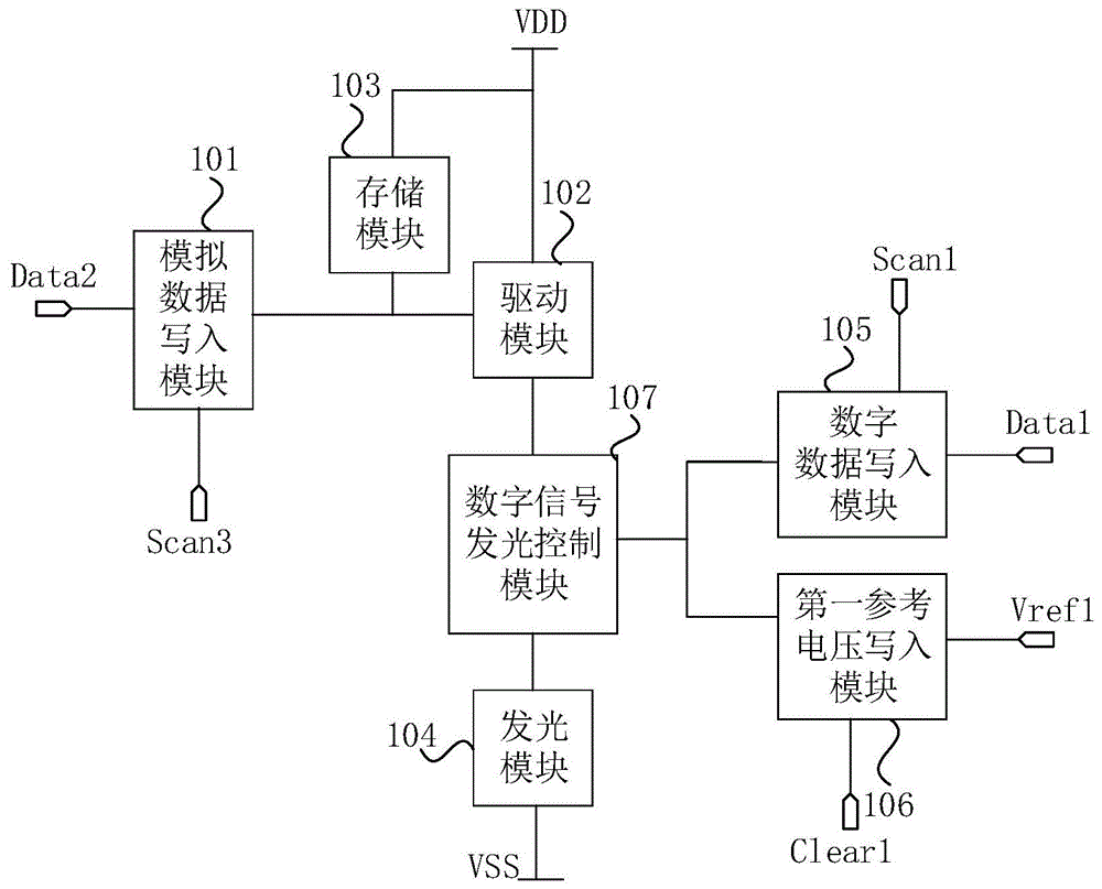
图1是本发明实施例提供的一种像素驱动电路的电路结构示意图,参见图1,像素驱动电路包括:模拟数据写入模块101、驱动模块102、存储模块103、发光模块104、数字数据写入模块105、第一参考电压写入模块106和数字信号发光控制模块107;模拟数据写入模块101用于将模拟数据写入驱动模块102,驱动模块102用于产生驱动电流,发光模块104用于响应驱动电流,存储模块103用于维持驱动模块102的控制端的电位;数字数据写入模块105用于将数字数据写入数字信号发光控制模块107的控制端,数字信号发光控制模块107根据数字数据导通;第一参考电压写入模块106用于将第一参考电压写入数字信号发光控制模块107的控制端,数字信号发光控制模块107根据第一参考电压关断。Fig. 1 is a schematic circuit structure diagram of a pixel driving circuit provided by an embodiment of the present invention. Referring to Fig. 1, the pixel driving circuit includes: an analog
具体地,发光模块104例如可以是OLED(Organic Light-Emitting Diode,有机发光二极管),OLED为电流型器件,需要在驱动电流的作用下才能够发光,驱动模块102可以根据模拟数据写入模块101写入的模拟数据产生相应的驱动电流,发光模块104根据驱动电流进行发光,从而实现模拟驱动的功能。数字数据写入模块105将数字数据写入数字信号发光控制模块107的控制端,从而导通数字信号发光控制模块107,因此,控制数字数据写入模块105的导通时间,即可控制数字信号发光控制模块107的导通时间,从而控制发光模块104的发光时间,进而实现数字驱动的功能。第一参考电压写入模块106将第一参考电压写入数字信号发光控制模块107的控制端,从而关断数字信号发光控制模块107,因此,控制第一参考电压写入模块106的导通时间,即可控制数字信号发光控制模块107的关断时间,从而控制发光模块104的发光时长。Specifically, the light-emitting
本实施例的像素驱动电路在显示待显示亮度时,首先判断待显示亮度是否满足预设条件,如果待显示亮度满足预设条件,则根据待显示亮度确定模拟数据,也即若满足预设条件,则采用模拟驱动,在模拟驱动的方式中,待显示亮度不同时,模拟数据不同;在数据写入阶段,将确定好的模拟数据写入驱动模块102;在发光阶段,数字数据写入模块105导通,将数字数据持续写入数字信号发光控制模块107,发光模块104按照模拟数据持续发光,从而实现发光模块104按照待显示亮度显示。如果待显示亮度不满足预设条件,则根据待显示亮度确定数字数据写入模块105的第一导通时间和第一参考电压写入模块106的第二导通时间,也即若不满足预设条件,则采用数字驱动的方式,在数据写入阶段,将模拟数据写入驱动模块102;发光阶段中,在第一导通时间,将数字数据持续写入数字信号发光控制模块107,发光模块104发光,在第二导通时间,将第一参考电压持续写入数字信号发光控制模块107,发光模块104关闭,从而使得发光模块104按照确定的第一导通时间发光,按照第二导通时间关闭,从而实现发光模块104按照待显示亮度显示。当满足预设条件时,使用模拟数据控制发光模块104的电流,从而达到待显示亮度,不满足预设条件时,使用数字数据控制发光模块104的发光时间,从而达到待显示亮度,从而可以实现不同的待显示亮度。因此,利用模拟数据和数字数据混合驱动,可以使得发光模块104实现不同的待显示亮度,即实现不同的显示灰阶,从而实现显示灰阶的完全展开。而且,利用模拟数据驱动可以避免数字数据驱动引起的灰阶跳变问题,实现了改善显示面板的显示效果,提高了显示面板显示亮度的均一性。When displaying the brightness to be displayed, the pixel driving circuit of this embodiment first judges whether the brightness to be displayed satisfies the preset condition. , the analog drive is adopted. In the analog drive mode, when the display brightness is different, the analog data is different; in the data writing stage, the determined analog data is written into the
其中,在数字驱动方式中,模拟数据为固定值,只有当待显示亮度满足预设条件时,也即只有在模拟驱动的方式中,才会根据待显示亮度改变模拟数据。Wherein, in the digital driving mode, the analog data is a fixed value, and only when the brightness to be displayed meets a preset condition, that is, only in the analog driving mode, the analog data will be changed according to the brightness to be displayed.
其中,预设条件例如可以是显示灰阶跳变,显示灰阶跳变例如是指待显示亮度对应的二进制数据与当前显示亮度对应的二进制数据各个位均相反;预设条件也可以是待显示亮度大于预设亮度,也可以是其他条件,具体可以根据实际情况进行确定,本实施方案并不进行限定。Among them, the preset condition can be, for example, a display grayscale jump, which means that each bit of the binary data corresponding to the brightness to be displayed is opposite to the binary data corresponding to the current display brightness; the preset condition can also be that the binary data to be displayed The brightness greater than the preset brightness may also be other conditions, which may be determined according to actual conditions, and are not limited in this embodiment.
另外,本实施例采用第一参考电压写入模块106控制数字信号发光控制模块107的关闭,从而实现控制发光模块104的关闭,由于数字信号发光控制模块107关闭,所以发光模块104中完全没有电流通过,因此,可以实现发光模块104的完全关断,不会存在残留亮度,从而实现准确控制发光模块104的关闭。而且,本实施例的技术方案相对于现有技术中改变模拟数据来强制关闭发光模块104更方便,并且通过控制第一参考电压写入模块106的导通时间,即可控制数字信号发光控制模块107的导通时间,从而可以控制发光模块104的关闭时间,从而更准确的实现待显示亮度。通常,数字数据的电压是不会变化的,所以通过数字数据的电压无法实现数字信号发光控制模块107的关闭。而且,如果可以只设置数字数据写入模块105,通过改变数字数据来实现数字信号发光控制模块107的导通和关闭,那么数字数据写入模块105就要一直导通,通过控制写入数字数据的时间来实现待显示亮度,但是数字数据的写入时间是难以准确控制的,而且数字数据的变化可能会导致灰阶的跳变,不利于灰阶的完全展开。因此,本实施例的技术方案通过设置数字数据写入模块105和第一参考电压写入模块106,通过控制数字数据写入模块105的第一导通时间和第一参考电压写入模块106的第二导通时间可以更准确的控制数字信号发光控制模块107的导通时间和关闭时间,从而更准确的实现待显示亮度,从而有利于灰阶的完全展开。而且数字数据写入模块105和第一参考电压写入模块106可以不同步开始工作,可在相同时刻分别处在不同子帧,实现更多的待显示亮度,从而有利于灰阶的完全展开。In addition, in this embodiment, the first reference
本实施例的技术方案,采用的像素驱动电路包括模拟数据写入模块、驱动模块、存储模块、发光模块、数字数据写入模块、第一参考电压写入模块和数字信号发光控制模块,如果待显示亮度满足预设条件,则根据待显示亮度确定模拟数据,将模拟数据写入驱动模块,使得发光模块按照模拟数据发光,实现待显示亮度;如果待显示亮度不满足预设条件,则根据待显示亮度确定数字数据写入模块的第一导通时间和第一参考电压写入模块的第二导通时间,利用第一导通时间和第二导通时间控制发光模块的发光时长,实现待显示亮度。利用模拟数据和数字数据的混合驱动,可以使得发光模块实现不同的待显示亮度,即实现不同的显示灰阶,从而实现显示灰阶的完全展开。而且,利用模拟数据驱动可以避免数字数据驱动引起的灰阶跳变问题,实现了改善显示面板的显示效果,提高了显示面板显示亮度的均一性。本实施例的技术方案解决了显示面板的显示灰阶难以完全展开,显示灰阶容易跳变的问题,达到了更好的灰阶展开的效果,并且可以准确控制发光模块的关闭,使得发光模块更好的显示待显示亮度,提高了显示面板的显示效果。In the technical solution of this embodiment, the pixel driving circuit used includes an analog data writing module, a driving module, a storage module, a light emitting module, a digital data writing module, a first reference voltage writing module and a digital signal lighting control module. If the display brightness meets the preset conditions, the analog data is determined according to the brightness to be displayed, and the analog data is written into the drive module, so that the light-emitting module emits light according to the analog data to realize the brightness to be displayed; if the brightness to be displayed does not meet the preset conditions, then according to the The display brightness determines the first conduction time of the digital data writing module and the second conduction time of the first reference voltage writing module, and uses the first conduction time and the second conduction time to control the light-emitting duration of the light-emitting module to realize the standby time. Display brightness. By using the mixed driving of analog data and digital data, the light-emitting module can realize different brightness to be displayed, that is, realize different display gray scales, so as to realize the complete expansion of the display gray scales. Moreover, the use of analog data driving can avoid the gray scale jump problem caused by digital data driving, thereby improving the display effect of the display panel and improving the uniformity of display brightness of the display panel. The technical solution of this embodiment solves the problem that the display gray scale of the display panel is difficult to fully expand and the display gray scale is easy to jump, achieves a better effect of gray scale expansion, and can accurately control the closing of the light-emitting module, so that the light-emitting module The brightness to be displayed is better displayed, and the display effect of the display panel is improved.
在上述实施方案的基础上,图2是本发明实施例提供的另一种像素驱动电路的电路结构示意图,可选地,参见图2,数字数据写入模块105包括第一晶体管T1,第一参考电压写入模块106包括第二晶体管T2;第一晶体管T1的控制端接入第一扫描信号Scan1,第一晶体管T1的第一端用于写入数字数据Data1,第一晶体管T1的第二端与数字信号发光控制模块107的控制端电连接;第二晶体管T2的控制端接入第一控制信号Clear1,第二晶体管T2的第一端用于写入第一参考电压Vref1,第二晶体管T2的第二端与数字信号发光控制模块107的控制端电连接。On the basis of the above-mentioned embodiments, FIG. 2 is a schematic circuit structure diagram of another pixel driving circuit provided by an embodiment of the present invention. Optionally, referring to FIG. 2 , the digital
具体地,第一扫描信号Scan1可以控制第一晶体管T1的导通和截止,利用第一扫描信号Scan1即可控制第一晶体管T1的导通时间,从而控制数字信号发光控制模块107的导通时间。第一晶体管T1可以为N型晶体管,也可以为P型晶体管,因为N型晶体管传输低电平更有效,P型晶体管传输高电平更有效,所以当写入第一晶体管T1的数字数据Data1为高电平时,第一晶体管T1为P型晶体管,当数字数据Data1为低电平时,第一晶体管T1为N型晶体管,图2中只示出了第一晶体管T1为N型晶体管的情况,但并不进行限定。第一控制信号Clear1可以控制第二晶体管T2的导通和截止,利用第一控制信号Clear1即可控制第二晶体管T2的导通时间,从而控制数字信号发光控制模块107的关闭时间。同理,第二晶体管T2可以为N型晶体管,也可以为P型晶体管,图2中只示出了第二晶体管T2为P型晶体管的情况,但并不进行限定。Specifically, the first scan signal Scan1 can control the turn-on and turn-off of the first transistor T1, and the turn-on time of the first transistor T1 can be controlled by using the first scan signal Scan1, thereby controlling the turn-on time of the digital signal light emitting
在上述实施方案的基础上,图3是本发明实施例提供的又一种像素驱动电路的电路结构示意图,可选地,参见图3,数字数据写入模块105还包括第三晶体管T3,第一参考电压写入模块106还包括第四晶体管T4;第三晶体管T3的控制端用于接入第二扫描信号Scan2,第三晶体管T3的第一端与第一晶体管T1的第一端电连接,第三晶体管T3的第二端与第一晶体管T1的第二端电连接;第一扫描信号Scan1与第二扫描信号Scan2相位相反,第一晶体管T1为N型晶体管,第三晶体管T3为P型晶体管;第四晶体管T4的控制端接入第二控制信号Clear2,第四晶体管T4的第一端与第二晶体管T2的第一端电连接,第四晶体管T4的第二端与第二晶体管T2的第二端电连接;第一控制信号Clear1与第二控制信号Clear2相位相反,第二晶体管T2为P型晶体管,第四晶体管T4为N型晶体管。On the basis of the above embodiments, FIG. 3 is a schematic circuit structure diagram of another pixel driving circuit provided by an embodiment of the present invention. Optionally, referring to FIG. 3 , the digital
具体地,设置第一晶体管T1为N型管,第三晶体管T3为P型管,可以使得无论数字数据Data1为低电平还是高电平,均可以有效传输,从而提高了像素驱动电路的驱动效率,并且,第一扫描信号Scan1与第二扫描信号Scan2相位相反,可以保证第一晶体管T1和第三晶体管T3同时导通,保证数字数据Data1可以写入到数字信号发光控制模块107。设置第三晶体管T3为P型管,第四晶体管T4为N型管,可以使得无论第一参考电压Vref1为低电平还是高电平,均可以有效传输,从而提高了像素驱动电路的驱动效率,并且,第一控制信号Clear1与第二控制信号Clear2相位相反,可以保证第二晶体管T2和第四晶体管T4同时导通,保证第一参考电压Vref1可以写入到数字信号发光控制模块107。Specifically, setting the first transistor T1 as an N-type transistor and the third transistor T3 as a P-type transistor can make it possible to effectively transmit the digital data Data1 regardless of whether it is at a low level or at a high level, thereby improving the driving performance of the pixel driving circuit. In addition, the first scan signal Scan1 and the second scan signal Scan2 have opposite phases, which can ensure that the first transistor T1 and the third transistor T3 are turned on at the same time, and ensure that the digital data Data1 can be written into the digital signal light
可选地,继续参考图2,像素驱动电路还包括锁存模块108;锁存模块108用于维持数字信号发光控制模块107的控制端的电位。Optionally, continuing to refer to FIG. 2 , the pixel driving circuit further includes a
具体地,锁存模块108具有数据暂存的作用,可以维持数字信号发光控制模块107的控制端的电位,使得数字信号发光控制模块107的控制端的电位不会被环境影响,只有当数字数据写入模块105写入的数字数据变化时,数字信号发光控制模块107的控制端的电位才会随之变化,保证了数字数据写入的准确性。Specifically, the
可选地,继续参考图2,锁存模块108包括第一反相器108a和第二反相器108b,第一反相器108a的输入端与数字信号发光控制模块107的控制端电连接,第一反相器108a的输出端与第二反相器108b的输入端电连接,第二反相器108b的输出端与第一晶体管T1的第二端电连接。Optionally, continuing to refer to FIG. 2, the
或者,图4是本发明实施例提供的又一种像素驱动电路的电路结构示意图,可选地,参见图4,锁存模块108包括第一电容C1,第一电容C1的第一端接入第一电源信号,第一电容C1的第二端与数字信号发光控制模块107的控制端电连接。Alternatively, FIG. 4 is a schematic circuit structure diagram of another pixel driving circuit provided by an embodiment of the present invention. Optionally, referring to FIG. 4 , the
具体地,锁存模块108可以包括第一反相器108a和第二反相器108b,可以实现信号的锁存和隔离,保证数字信号发光控制模块107的控制端的电位不会被环境影响,从而维持数字信号发光控制模块107的控制端的电位,保证了数字数据写入的准确性。另外,第一反相器108a和第二反相器108b还具有数据整形的作用。Specifically, the
或者,锁存模块108可以包括第一电容C1,第一电容C1具有存储能量的作用,从而可以维持数字信号发光控制模块107的控制端的电位,电容成本低,可以降低像素驱动电路的成本。Alternatively, the
可选地,继续参考图1,模拟数据写入模块101的控制端接入第三扫描信号Scan3,模拟数据写入模块101的第一端用于写入模拟数据Data2,模拟数据写入模块101的第二端与驱动模块102的控制端电连接;驱动模块102的第一端用于连接第一电源信号,驱动模块102的第二端与数字信号发光控制模块107的第一端电连接,数字信号发光控制模块107的第二端与发光模块104的第一端电连接,发光模块104的第二端连接第二电源信号;存储模块103的第一端连接第一电源信号,存储模块103的第二端与驱动模块102的控制端电连接;数字数据写入模块105的第一端接入数字数据Data1,数字数据写入模块105的第二端与数字信号发光控制模块107的控制端电连接;第一参考电压写入模块106的第一端接入第一参考电压Vref1,第一参考电压写入模块106的第二端与数字信号发光控制模块107的控制端电连接。Optionally, continuing to refer to FIG. 1 , the control terminal of the analog data writing module 101 is connected to the third scanning signal Scan3, and the first end of the analog data writing module 101 is used to write the analog data Data2, and the analog data writing module 101 The second end of the drive module 102 is electrically connected to the control end; the first end of the drive module 102 is used to connect the first power supply signal, and the second end of the drive module 102 is electrically connected to the first end of the digital signal lighting control module 107, The second end of the digital signal lighting control module 107 is electrically connected to the first end of the light emitting module 104, and the second end of the light emitting module 104 is connected to the second power signal; the first end of the storage module 103 is connected to the first power signal, and the storage module 103 The second end of the digital data writing module 105 is electrically connected to the control end of the drive module 102; the first end of the digital data writing module 105 is connected to the digital data Data1, and the second end of the digital data writing module 105 is connected to the control end of the digital signal lighting control module 107 Electrical connection: the first terminal of the first reference voltage writing module 106 is connected to the first reference voltage Vref1 , and the second terminal of the first reference voltage writing module 106 is electrically connected to the control terminal of the digital signal lighting control module 107 .
具体地,通过第三扫描信号Scan3可以控制模拟数据写入模块101导通和截止,当模拟数据写入模块101导通时,可以将模拟数据Data2写入驱动模块102,驱动模块102产生相应的驱动电流,当数字数据写入模块105导通时,将数字数据Data1写入数字信号发光控制模块107,使得数字信号发光控制模块107导通,发光模块104就可以根据驱动电流进行发光。当第一参考电压写入模块106导通时,将第一参考电压Vref1写入数字信号发光控制模块107,使得数字信号发光控制模块107截止,发光模块104无法获取驱动电流而关闭。因此,通过控制数字数据写入模块105的第一导通时间和第一参考电压写入模块106的第二导通时间,即可控制数字信号发光控制模块107的导通时间和截止时间,从而控制发光模块104的发光时长。Specifically, the analog
在上述技术方案的基础上,图5是本发明实施例提供的又一种像素驱动电路的电路结构示意图,可选地,参见图5,模拟数据写入模块101包括第五晶体管T5,驱动模块102包括第六晶体管T6,存储模块103包括第二电容C2,发光模块104包括有机发光二极管D1。第五晶体管T5的控制端为模拟数据写入模块101的控制端,第五晶体管T5的第一端为模拟数据写入模块101的第一端,第五晶体管T5的第二端为模拟数据写入模块101的第二端。第六晶体管T6的控制端为驱动模块102的控制端,第六晶体管T6的第一端为驱动模块102的第一端,第六晶体管T6的第二端为驱动模块102的第二端。第二电容C2的第一端为存储模块103的第一端,第二电容C2的第二端为存储模块103的第二端。有机发光二极管D1的阳极为发光模块104的第一端,有机发光二极管D1的阴极为发光模块104的第二端。第一电源信号为电压VDD,第二电源信号为电压VSS。数字信号发光控制模块107包括第七晶体管T7,第七晶体管T7的控制端为数字信号发光控制模块107的控制端,第七晶体管T7的第一端为数字信号发光控制模块107的第一端,第七晶体管T7的第二端为数字信号发光控制模块107的第二端。图5中只示出了数字数据写入模块105包括第一晶体管T1和第三晶体管T3,第一参考电压写入模块106包括第二晶体管T2和第四晶体管T4的情况,但并不进行限定。On the basis of the above technical solution, FIG. 5 is a schematic circuit structure diagram of another pixel driving circuit provided by an embodiment of the present invention. Optionally, referring to FIG. 5 , the analog
图6是本发明实施例提供的又一种像素驱动电路的电路结构示意图,可选地,参见图6,像素驱动电路还包括第一初始化模块109、第二初始化模块110、阈值补偿模块111、第一模拟信号发光控制模块112和第二模拟信号发光控制模块113;第一初始化模块109的控制端接入第四扫描信号Scan4,第一初始化模块109的第一端接入第二参考电压Vref2,第一初始化模块109的第二端与驱动模块102的控制端电连接,存储模块103的第一端与驱动模块102的控制端电连接,存储模块103的第二端连接第一电源信号;第一初始化模块109用于初始化驱动模块102;第二初始化模块110的控制端接入第四扫描信号Scan4,第二初始化模块110的第一端接入第二参考电压Vref2,第二初始化模块110的第二端与发光模块104的第一端电连接;第二初始化模块110用于初始化发光模块104;模拟数据写入模块101的控制端接入第三扫描信号Scan3,模拟数据写入模块101的第一端用于写入模拟数据Data2,模拟数据写入模块101的第二端与驱动模块102的第一端电连接;驱动模块102的第一端与第一模拟信号发光控制模块112的第一端电连接,驱动模块102的第二端与第二模拟信号发光控制模块113的第一端电连接;第一模拟信号发光控制模块112的控制端接入使能信号EM,第一模拟信号发光控制模块112的第二端与第一电源信号电连接;阈值补偿模块111的控制端接入第三扫描信号Scan3,阈值补偿模块111的第一端与驱动模块102的控制端电连接,阈值补偿模块111的第二端与第二模拟信号发光控制模块113的第一端电连接;阈值补偿模块111用于抓取驱动模块102的阈值电压至驱动模块102的控制端;第二模拟信号发光控制模块113的控制端接入使能信号EM,第二模拟信号发光控制模块113的第二端与数字信号发光控制模块107电连接。Fig. 6 is a schematic circuit structure diagram of another pixel driving circuit provided by an embodiment of the present invention. Optionally, referring to Fig. 6, the pixel driving circuit further includes a first initialization module 109, a second initialization module 110, a threshold compensation module 111, The first analog signal lighting control module 112 and the second analog signal lighting control module 113; the control terminal of the first initialization module 109 is connected to the fourth scanning signal Scan4, and the first terminal of the first initialization module 109 is connected to the second reference voltage Vref2 , the second end of the first initialization module 109 is electrically connected to the control end of the drive module 102, the first end of the storage module 103 is electrically connected to the control end of the drive module 102, and the second end of the storage module 103 is connected to the first power supply signal; The first initialization module 109 is used to initialize the drive module 102; the control terminal of the second initialization module 110 is connected to the fourth scan signal Scan4, the first terminal of the second initialization module 110 is connected to the second reference voltage Vref2, and the second initialization module 110 The second end of the second end is electrically connected to the first end of the light-emitting module 104; the second initialization module 110 is used to initialize the light-emitting module 104; the control end of the analog data writing module 101 is connected to the third scanning signal Scan3, and the analog data writing module 101 The first end of the first end is used to write the analog data Data2, the second end of the analog data writing module 101 is electrically connected to the first end of the driving module 102; the first end of the driving module 102 is connected to the first analog signal light emitting control module 112 The first end is electrically connected, and the second end of the driving module 102 is electrically connected to the first end of the second analog signal light emitting control module 113; the control end of the first analog signal light emitting control module 112 is connected to the enable signal EM, and the first analog signal The second end of the signal lighting control module 112 is electrically connected to the first power supply signal; the control end of the threshold compensation module 111 is connected to the third scan signal Scan3, and the first end of the threshold compensation module 111 is electrically connected to the control end of the drive module 102, The second end of the threshold compensation module 111 is electrically connected to the first end of the second analog signal lighting control module 113; the threshold compensation module 111 is used to capture the threshold voltage of the driving module 102 to the control end of the driving module 102; the second analog signal The control terminal of the lighting control module 113 is connected to the enable signal EM, and the second terminal of the second analog signal lighting control module 113 is electrically connected to the digital signal lighting control module 107 .
具体地,图7是本发明实施例提供的一种像素驱动电路的时序图,参见图7,在初始化阶段t1,第四扫描信号Scan4为低电平,第四扫描信号Scan4控制第一初始化模块109和第二初始化模块110导通,使得第二参考电压Vref2写入第一初始化模块109和第二初始化模块110,从而初始化驱动模块102和发光模块104。在模拟数据写入和阈值补偿阶段t2,第三扫描信号Scan3为低电平,第三扫描信号Scan3控制模拟数据写入模块101导通,使得模拟数据Data2通过模拟数据写入模块101写入驱动模块102,同时阈值补偿模块111导通,进行阈值补偿,使得流过发光模块104的电流大小与驱动模块102的阈值电压无关。在发光阶段t3,使能信号EM为低电平,从而控制第一模拟信号发光控制模块112和第二模拟信号发光控制模块113导通,并且第一扫描信号Scan1控制数字数据写入模块105导通,使得数字数据Data1写入数字信号发光控制模块107,从而使得数字信号发光控制模块107也导通,从而发光模块104导通,发光模块104发光。图8是本发明实施例提供的另一种像素驱动电路的时序图,参见图8,图8中横坐标表示时间,纵坐标表示像素行数,图8中只示出了行数为16的情况,但并不进行限定,图8中的实线表示第一扫描信号Scan1,虚线表示第一控制信号Clear1,SF1、SF2、SF3和SF4表示不同待显示亮度对应的扫描时间段,因此,在发光阶段,可以根据待显示亮度来确定第一扫描信号Scan1的扫描时间和第一控制信号Clear1的扫描时间,从而控制数字数据写入模块105的第一导通时间和第一参考电压写入模块106的第二导通时间,从而控制数字信号发光控制模块107的导通时间和截止时间,从而控制发光模块104按照待显示亮度发光,从而实现不同的显示灰阶。但是,在当前显示亮度和待显示亮度较大时,控制数字信号发光控制模块107的导通时间和截止时间来控制发光模块104显示待显示亮度可能不容易实现,这时可以根据待显示亮度调节模拟数据Data2,从而控制发光模块104的电流,从而使得发光模块104显示待显示亮度。而且,第一扫描信号Scan1的扫描时间是二进制数据,当待显示亮度对应的二进制数据与当前显示亮度对应的二进制数据各个位均相反时,发光模块104的显示灰阶容易发生跳变,这时,可以根据待显示亮度调节模拟数据Data2,从而控制发光模块104的电流,从而使得发光模块104显示待显示亮度。因此,通过数字数据和模拟数据的混合驱动,即可实现显示灰阶更好的展开,更好的实现不同的显示灰阶,还可以避免数字数据驱动引起的灰阶跳变问题,实现了改善显示面板的显示效果,提高了显示面板显示亮度的均一性。Specifically, FIG. 7 is a timing diagram of a pixel driving circuit provided by an embodiment of the present invention. Referring to FIG. 7, in the initialization phase t1, the fourth scan signal Scan4 is at a low level, and the fourth scan signal Scan4 controls the
图9是本发明实施例提供的又一种像素驱动电路的电路结构示意图,可选地,参见图9,第一初始化模块109包括第八晶体管T8,第八晶体管T8的控制端为第一初始化模块109的控制端,第八晶体管T8的第一端为第一初始化模块109的第一端,第八晶体管T8的第二端为第一初始化模块109的第二端。第二初始化模块110包括第九晶体管T9,第九晶体管T9的控制端为第二初始化模块110的控制端,第九晶体管T9的第一端为第二初始化模块110的第一端,第九晶体管T9的第二端为第二初始化模块110的第二端。阈值补偿模块111包括第十晶体管T10,第十晶体管T10的控制端为阈值补偿模块111的控制端,第十晶体管T10的第一端为阈值补偿模块111的第一端,第十晶体管T10的第二端为阈值补偿模块111的第二端。第一模拟信号发光控制模块112包括第十一晶体管T11,第十一晶体管T11的控制端为第一模拟信号发光控制模块112的控制端,第十一晶体管T11的第一端为第一模拟信号发光控制模块112的第一端,第十一晶体管T11的第二端为第一模拟信号发光控制模块112的第二端。第二模拟信号发光控制模块113包括第十二晶体管T12,第十二晶体管T12的控制端为第二模拟信号发光控制模块113的控制端,第十二晶体管T12的第一端为第二模拟信号发光控制模块113的第一端,第十二晶体管T12的第二端为第二模拟信号发光控制模块113的第二端。FIG. 9 is a schematic circuit structure diagram of another pixel driving circuit provided by an embodiment of the present invention. Optionally, referring to FIG. 9, the
本实施例还提供了一种像素驱动电路的驱动方法,用于驱动上述任意技术方案所述的像素驱动电路,图10是本发明实施例提供的一种像素驱动电路的驱动方法的流程图,参见图10,像素驱动电路的驱动方法包括:This embodiment also provides a driving method for a pixel driving circuit, which is used to drive the pixel driving circuit described in any of the above technical solutions. FIG. 10 is a flowchart of a driving method for a pixel driving circuit provided in an embodiment of the present invention. Referring to Figure 10, the driving method of the pixel driving circuit includes:
S101、获取待显示亮度。S101. Obtain brightness to be displayed.
S102、判断待显示亮度是否满足预设条件;若是,则执行S103,若否,则执行S104。S102. Determine whether the brightness to be displayed satisfies a preset condition; if yes, execute S103; if not, execute S104.
S103、根据待显示亮度确定模拟数据;在数据写入阶段将模拟数据写入驱动模块,并在发光阶段将数字数据持续写入数字信号发光控制模块。S103. Determine the analog data according to the brightness to be displayed; write the analog data into the drive module during the data writing phase, and continuously write the digital data into the digital signal light emitting control module during the light emitting phase.
S104、根据待显示亮度确定数字数据写入模块的第一导通时间以及第一参考电压写入模块的第二导通时间;在数据写入阶段将模拟数据写入驱动模块,并在第一导通时间将数字数据写入数字发光控制模块的控制端,在第二导通时间将第一参考电压写入数字发光控制模块的控制端,其中,模拟数据为固定值。S104. Determine the first conduction time of the digital data writing module and the second conduction time of the first reference voltage writing module according to the brightness to be displayed; write the analog data into the drive module in the data writing phase, and The digital data is written into the control terminal of the digital light emitting control module during the conduction time, and the first reference voltage is written into the control terminal of the digital light emitting control module during the second conduction time, wherein the analog data is a fixed value.
本实施例的驱动方法具体工作过程可参考本发明实施例关于像素驱动电路部分的描述,在此不再赘述。利用模拟数据和数字数据的混合驱动,可以使得发光模块实现不同的待显示亮度,即实现不同的显示灰阶,从而实现显示灰阶的完全展开。而且,利用模拟数据驱动可以避免数字数据驱动引起的灰阶跳变问题,实现了改善显示面板的显示效果,提高了显示面板显示亮度的均一性。For the specific working process of the driving method in this embodiment, reference may be made to the description of the pixel driving circuit in the embodiment of the present invention, which will not be repeated here. By using the mixed driving of analog data and digital data, the light-emitting module can realize different brightness to be displayed, that is, realize different display gray scales, so as to realize the complete expansion of the display gray scales. Moreover, the use of analog data driving can avoid the gray scale jump problem caused by digital data driving, thereby improving the display effect of the display panel and improving the uniformity of display brightness of the display panel.
可选地,预设条件包括:待显示亮度大于预设亮度,或者,待显示亮度对应的二进制数据与当前显示亮度的对应的二进制数据各个位均相反。Optionally, the preset condition includes: the brightness to be displayed is greater than the preset brightness, or each bit of the binary data corresponding to the brightness to be displayed is opposite to that of the binary data corresponding to the current display brightness.
图11是本发明实施例提供的一种显示面板的结构示意图,参考图11,显示面板包括多个本发明任意实施例提供的像素驱动电路PX,显示面板可包括多条纵横交错的扫描线(S1~Sk)与数据线(DL1~DLj),像素驱动电路位于扫描线与数据线限定出的区域,扫描线例如可以包括第一扫描线、第二扫描线、第三扫描线,为像素驱动电路PX提供扫描信号。因其包括本发明任意实施例提供的像素驱动电路,因而也又有相同的有益效果,在此不再赘述。Fig. 11 is a schematic structural diagram of a display panel provided by an embodiment of the present invention. Referring to Fig. 11, the display panel includes a plurality of pixel drive circuits PX provided in any embodiment of the present invention, and the display panel may include a plurality of criss-cross scanning lines ( S1~Sk) and data lines (DL1~DLj), the pixel drive circuit is located in the area defined by the scan line and the data line. Circuit PX provides scan signals. Because it includes the pixel driving circuit provided by any embodiment of the present invention, it also has the same beneficial effect, and will not be repeated here.
图12是本发明实施例提供的一种显示装置的结构示意图,参考图12,显示装置包括本发明任意实施例提供的显示面板,显示装置可为手机、平板、显示器、智能手表、MP3、MP4或其他可穿戴设备等,因其包含本发明任意实施例提供的显示面板,因而也具有相同的有益效果,在此不再赘述。Fig. 12 is a schematic structural diagram of a display device provided by an embodiment of the present invention. Referring to Fig. 12, the display device includes a display panel provided by any embodiment of the present invention, and the display device can be a mobile phone, a tablet, a monitor, a smart watch, MP3, MP4 Or other wearable devices, etc., because they include the display panel provided by any embodiment of the present invention, they also have the same beneficial effect, and will not be repeated here.
注意,上述仅为本发明的较佳实施例及所运用技术原理。本领域技术人员会理解,本发明不限于这里所述的特定实施例,对本领域技术人员来说能够进行各种明显的变化、重新调整和替代而不会脱离本发明的保护范围。因此,虽然通过以上实施例对本发明进行了较为详细的说明,但是本发明不仅仅限于以上实施例,在不脱离本发明构思的情况下,还可以包括更多其他等效实施例,而本发明的范围由所附的权利要求范围决定。Note that the above are only preferred embodiments of the present invention and applied technical principles. Those skilled in the art will understand that the present invention is not limited to the specific embodiments described herein, and that various obvious changes, readjustments and substitutions can be made by those skilled in the art without departing from the protection scope of the present invention. Therefore, although the present invention has been described in detail through the above embodiments, the present invention is not limited to the above embodiments, and can also include more other equivalent embodiments without departing from the concept of the present invention, and the present invention The scope is determined by the scope of the appended claims.
Claims (10)
Priority Applications (1)
| Application Number | Priority Date | Filing Date | Title |
|---|---|---|---|
| CN202110739724.8A CN115547233B (en) | 2021-06-30 | 2021-06-30 | Pixel driving circuit, driving method thereof and display panel |
Applications Claiming Priority (1)
| Application Number | Priority Date | Filing Date | Title |
|---|---|---|---|
| CN202110739724.8A CN115547233B (en) | 2021-06-30 | 2021-06-30 | Pixel driving circuit, driving method thereof and display panel |
Publications (2)
| Publication Number | Publication Date |
|---|---|
| CN115547233A true CN115547233A (en) | 2022-12-30 |
| CN115547233B CN115547233B (en) | 2025-12-09 |
Family
ID=84705589
Family Applications (1)
| Application Number | Title | Priority Date | Filing Date |
|---|---|---|---|
| CN202110739724.8A Active CN115547233B (en) | 2021-06-30 | 2021-06-30 | Pixel driving circuit, driving method thereof and display panel |
Country Status (1)
| Country | Link |
|---|---|
| CN (1) | CN115547233B (en) |
Cited By (2)
| Publication number | Priority date | Publication date | Assignee | Title |
|---|---|---|---|---|
| WO2024197572A1 (en) * | 2023-03-28 | 2024-10-03 | Boe Technology Group Co. Ltd. | Pixel driving circuit, display apparatus, and display method |
| US12586525B2 (en) | 2023-03-28 | 2026-03-24 | Beijing Boe Display Technology Co., Ltd. | Pixel driving circuit with driving current controlled by digital signals for grayscale control, display device and display method |
Citations (11)
| Publication number | Priority date | Publication date | Assignee | Title |
|---|---|---|---|---|
| US20030214493A1 (en) * | 2002-05-17 | 2003-11-20 | Hajime Akimoto | Image display |
| JP2004139042A (en) * | 2002-09-24 | 2004-05-13 | Seiko Epson Corp | Electronic circuit, electro-optical device, method of driving electro-optical device, and electronic apparatus |
| WO2009082056A1 (en) * | 2007-12-24 | 2009-07-02 | Syncoam Co., Ltd | Hybrid driving device and method of amoled panel using multi-analog gradation current |
| US20100039454A1 (en) * | 2008-08-13 | 2010-02-18 | Hitachi Displays, Ltd. | Display device |
| CN109872676A (en) * | 2019-04-22 | 2019-06-11 | 云谷(固安)科技有限公司 | A kind of digital drive pixel circuit and display device |
| US20200211464A1 (en) * | 2018-06-29 | 2020-07-02 | Boe Technology Group Co., Ltd. | Pixel circuit and driving method thereof, and display panel |
| WO2020233024A1 (en) * | 2019-05-21 | 2020-11-26 | 合肥维信诺科技有限公司 | Pixel circuit and display device |
| CN112233607A (en) * | 2020-09-11 | 2021-01-15 | 成都辰显光电有限公司 | Digital pixel driving circuit and driving method thereof, and display panel |
| CN112771600A (en) * | 2019-08-14 | 2021-05-07 | 京东方科技集团股份有限公司 | Pixel circuit, driving method thereof, array substrate and display device |
| CN112908247A (en) * | 2021-03-01 | 2021-06-04 | 成都辰显光电有限公司 | Pixel circuit, driving method thereof and display panel |
| CN112967668A (en) * | 2021-03-01 | 2021-06-15 | 成都辰显光电有限公司 | Pixel circuit, driving method thereof and display panel |
-
2021
- 2021-06-30 CN CN202110739724.8A patent/CN115547233B/en active Active
Patent Citations (11)
| Publication number | Priority date | Publication date | Assignee | Title |
|---|---|---|---|---|
| US20030214493A1 (en) * | 2002-05-17 | 2003-11-20 | Hajime Akimoto | Image display |
| JP2004139042A (en) * | 2002-09-24 | 2004-05-13 | Seiko Epson Corp | Electronic circuit, electro-optical device, method of driving electro-optical device, and electronic apparatus |
| WO2009082056A1 (en) * | 2007-12-24 | 2009-07-02 | Syncoam Co., Ltd | Hybrid driving device and method of amoled panel using multi-analog gradation current |
| US20100039454A1 (en) * | 2008-08-13 | 2010-02-18 | Hitachi Displays, Ltd. | Display device |
| US20200211464A1 (en) * | 2018-06-29 | 2020-07-02 | Boe Technology Group Co., Ltd. | Pixel circuit and driving method thereof, and display panel |
| CN109872676A (en) * | 2019-04-22 | 2019-06-11 | 云谷(固安)科技有限公司 | A kind of digital drive pixel circuit and display device |
| WO2020233024A1 (en) * | 2019-05-21 | 2020-11-26 | 合肥维信诺科技有限公司 | Pixel circuit and display device |
| CN112771600A (en) * | 2019-08-14 | 2021-05-07 | 京东方科技集团股份有限公司 | Pixel circuit, driving method thereof, array substrate and display device |
| CN112233607A (en) * | 2020-09-11 | 2021-01-15 | 成都辰显光电有限公司 | Digital pixel driving circuit and driving method thereof, and display panel |
| CN112908247A (en) * | 2021-03-01 | 2021-06-04 | 成都辰显光电有限公司 | Pixel circuit, driving method thereof and display panel |
| CN112967668A (en) * | 2021-03-01 | 2021-06-15 | 成都辰显光电有限公司 | Pixel circuit, driving method thereof and display panel |
Cited By (4)
| Publication number | Priority date | Publication date | Assignee | Title |
|---|---|---|---|---|
| WO2024197572A1 (en) * | 2023-03-28 | 2024-10-03 | Boe Technology Group Co. Ltd. | Pixel driving circuit, display apparatus, and display method |
| WO2024198032A1 (en) * | 2023-03-28 | 2024-10-03 | 京东方科技集团股份有限公司 | Pixel driving circuit, display device and display method |
| EP4609378A4 (en) * | 2023-03-28 | 2025-11-12 | Boe Technology Group Co Ltd | PIXEL DRIVER CIRCUIT, DISPLAY DEVICE AND DISPLAY METHOD |
| US12586525B2 (en) | 2023-03-28 | 2026-03-24 | Beijing Boe Display Technology Co., Ltd. | Pixel driving circuit with driving current controlled by digital signals for grayscale control, display device and display method |
Also Published As
| Publication number | Publication date |
|---|---|
| CN115547233B (en) | 2025-12-09 |
Similar Documents
| Publication | Publication Date | Title |
|---|---|---|
| CN109859682B (en) | Driving circuit, driving method thereof and display device | |
| CN113421514B (en) | Pixel circuit, driving method thereof, display panel and display device | |
| CN111754921B (en) | Pixel circuit | |
| CN108877611B (en) | Pixel driving circuit sensing method and pixel driving circuit | |
| CN112837649B (en) | Pixel driving circuit, driving method thereof, display panel and display device | |
| CN113593481A (en) | Display panel and driving method thereof | |
| US11222594B2 (en) | Digital pixel driving circuit and digital pixel driving method | |
| CN111354308A (en) | Pixel driving circuit, organic light-emitting display panel and display device | |
| CN116682358B (en) | Pixel circuits, pixel circuit driving methods, and display panels | |
| CN106847179A (en) | A kind of pixel compensation circuit and display device | |
| CN103971643B (en) | A kind of organic light-emitting diode pixel circuit and display device | |
| CN111754933A (en) | Pixel digital driving circuit, display device and driving method | |
| CN111710297B (en) | Pixel driving circuit, driving method thereof and display panel | |
| CN116168647A (en) | Pixel circuit, driving method thereof, and display panel | |
| CN115731870A (en) | A pixel driving circuit, light emission control method and display panel | |
| CN109903727B (en) | Digital drive pixel circuit, display panel and display device | |
| CN115547233A (en) | A pixel driving circuit, its driving method, and a display panel | |
| CN117059037B (en) | Pixel driving circuit and its driving method, display panel | |
| KR20210092306A (en) | Pixel circuit, display device and method of driving pixel circuit | |
| CN115035861B (en) | Pixel circuits and their driving methods, display panels | |
| CN117475918A (en) | Pixel drive circuit and display panel | |
| CN116312376A (en) | A pixel circuit, its driving method, and a display panel | |
| CN212276783U (en) | Pixel circuit | |
| EP4510116A1 (en) | Pixel driving circuit, driving method thereof, and display panel | |
| CN114203096B (en) | Pixel driving circuit, driving method thereof and display device |
Legal Events
| Date | Code | Title | Description |
|---|---|---|---|
| PB01 | Publication | ||
| PB01 | Publication | ||
| SE01 | Entry into force of request for substantive examination | ||
| SE01 | Entry into force of request for substantive examination | ||
| GR01 | Patent grant | ||
| GR01 | Patent grant |